universiti sains malaysia...
TRANSCRIPT

A 2.4 GHZ MIMO WIRELESS TRANSCEIVER DESIGN
By
YAZEED M.A QASAYMEH
Thesis submitted in fulfillment of the requirement
For the degree of Master of Science
UNIVERSITI SAINS MALAYSIA
2008

DEDICATION
Praise be to Allah, the most gracious and the most merciful. Without his blessing and
guidance my accomplishments would never have been possible.
My father mohd Ibrahim and my mother yusra mohd for their patience and support for
all these years
My fiancée who always light up for me.
My supervisor mohd fadzil ain.
ii

ACKNOWLEDGMENT
I would like to express my thanks and appreciation to my supervisors, Dr. Mohd Fadzil
Ain and Dr Mohd Ansor Yosuf for their continuous encouragement and kind help in my
research and study and for their invaluable advice and comments from deciding the
thesis topic to revising the writing. Their guidance and consistent encouragement
allowed me complete this work. I am extremely impressed with their teaching, advising
and generosity. I have realized how truly fortunate I am to have such an open-minded
supervisors who has incredible vision and boundless energy.
Further thanks to my research group Azman Zakaria, Mohd Arrif and for help, support,
and friendship during my darkest time.
I would also like to acknowledge my friends Mohd batah, Anas Quitshat, Lily Tiong and
Rabie Ali for their supportive opinion
Finally I would like to thank Mr. Latip Hamid, Mr. Ellias, Mr. Zuber, and Mr. Hisham
for their help during my research in USM
iii

TABLE OF CONTENTS
TITLE……………………………………………………………………………...... i
DEDICATION…………………………………………………………………….... ii
ACKNOWLEDGMENT……………………………………………………………. iii
TABLE OF CONTENTS…………………………………………………………… iv
LIST OF TABLES………………………………………………………………….. viii
LIST OF FIGURES………………………………………………………………… ix
ABBREVIATION…………………………………………………………………...
ABSTRAK…………………………………………………………………………..
xii
xiv
ABSTRACT………………………………………………………………………… xv
CHAPTER ONE: INTRODUCTION……………………………………………… 1
1.1 Background……………………………………………………………………... 1
1.2 Motivation………………………………………………………………………. 2
1.3 Objectives……………………………………………………………………….. 3
1.4 Thesis outline……………………………………………………………………
3
CHAPTER TWO: LITERATURE REVIEW…………….………………………... 4
2.1 Introduction……………………………………………………………………... 4
2.2 Theory of communication systems……………………………………………... 5
iv

2.2 Transmitter……………………………………………………………………
2.2.1 Quadrature signal linearization…………………………………………
2.2.2 Transmitter types………………………………………………………..
6
7
8
2.2.1.1 Super-heterodyne transmitter…………………….…………..
2.2.1.2 Direct conversion transmitter (homodyne)……………………
9
10
2.2.2 Receiver…………………………………………………………………...
2.2.2.1 Quadrature signal imbalance….…………………………………..
2.2.2.2Receiver types………………...……………………………………
11
13
14
2.2.2.1 Super heterodyne Receiver………...…………………….. 15
2.2.2.2 Direct-Conversion Receiver (Homodyne)……………...... 16
2.2.2.3 Low-IF Receiver…………………………………………. 17
2.2.2.5 Wideband IF receiver………………………...................... 19
2.2.3 Receiver Specification………………………………………………. 20
2.2.3.1 Receiver sensitivity……………………………………….. 20
2.2.3.2 Receiver selectivity………...……………………………... 21
2.2.3 Communication channel………………………………………………….. 22
2.2.3.1 Cables……………………………………………………………... 22
2.2.3.2 Fiber optic………………………………………………………… 22
2.2.3.3 Free space…………………………………………………………. 23
CHPATER THREE: MIMO WIRELESS TRANSCEIVER DESIGN…………… 24
3.1 Introduction……………………………………………………………………... 24
3.2 Simulation and fabrication software……………………………………………. 24
3.2.1 Circuit simulation…………………………………………………………. 25
v

3.2.2 PCB layout and fabrication………………………………………………..
3.2.3 Matlab……………………………………………………………………..
29
30
3.3 Prototype assembly…………………………………………………………….. 30
3.4 Test and measurement………………………………………………………….. 30
3.4.1 Transmitter Design………………………………………………………... 31
3.4.1.1 Digital to analog converter (AD9708)………………………………….. 31
3.4.1.2 DAC amplifier (AD8072)………………………………………………. 32
3.4.1.3 IQ modulator (RF2422)………………………………………………… 33
3.4.1.4 Power amplifier (RF2126)……………………………………………… 34
3.4.1.5 Complete transmitter……………………………………………………. 36
3.4.2 Receiver design…………………………………………………………… 37
3.4.2.1 Low noise amplifier (RF2304)………………………………………….. 37
3.4.2.3 Downconverter (MAX2682)…………………….…………………….. 38
3.4.2.3 IQ Demodulator (RF2713)……………………………………………… 39
3.4.2.3 Analog to digital converter (ADC08100)….…………………………... 41
3.4.2.4 Complete receiver……………………………………………………….
42
CHAPTER FOUR: SIMULATION RESULTS AND DISCUSSION….…………. 43
4.1 Simulation results………………………………………………………………. 43
4.1.1 Transmitter simulation……………………………………………………. 43
4.1.2 Receiver simulation………………………………………………………. 46
4.2 Printed circuit board fabrication………………………………………………... 49
4.2.1 Digital to analog converter………………………………………………... 49
vi

4.2.2 I-Q modulator…………………………………………………………….. 50
4.2.3 Power linear amplifier…………………………………………………….. 51
4.2.4 Low noise amplifier………………………………………………………. 52
4.2.5 Downconverter……………………………………………………………. 53
4.2.6 I-Q demodulator……………………………………………………........... 54
4.2.7 Analog to digital converter……………………………………………...... 55
4.3 Outputs from the Measurements………………………………………………... 57
4.3.1 I-Q Matlab signal………………………………………………………….. 57
4.3.2 Digital to analog converter………………………………………………… 59
4.3.3 Modulator………………………………………………………………….. 59
4.3.4 Linear Power amplifier……………………………………………………. 60
4.3.5 Complete transmitter……………………………........................................ 62
4.3.5 Low noise amplifier……………………………………………………….. 63
4.3.6 Downconverter……………………………………………………………. 65
4.3.7 I-Q demodulator…………………………………………………………… 67
4.3.8 Analog to digital converter……………………………………………….. 69
4.3.10 complete receiver…………………………………………………………
70
CHAPTER FIVE: CONCLUSION AND FUTURE WORK……………………... 72
5.1 Conclusion……………………………………………………………………… 72
5.2 Future work……………………………………………………………………. 74
REFERENCES……………………………………………………………………. 75
APPENDIX………..................................................................................................... 77
vii

LIST OF TABLES Page
Table 4.1: Modulator power gain at different VCC voltage 59
59
Table 4.2: Linear power amplifier power gain at different VCC voltage 61 61
Table 4.3: Transmitter power gain at different frequencies 63 63
Table 4.4: Low noise amplifier power gain at different frequencies 63 63
Table 4.5: Down converter power gain at different VCC voltage 64
Table 4.6: Receiver power gain at different input power levels. 71
64
71
viii

LIST OF FIGURES Page
Figure 2.1: Basic element of communication system 5
Figure 2.2: Quadrature transmitter architecture 9
Figure 2.3: Super-heterodyne transmitter 10
Figure 2.4: Direct conversion transmitter 11
Figure 2.5: Super heterodyne Receiver 15
Figure 2.6: Direct-Conversion Receiver 17
Figure 2.7: Low-IF Receiver 18
Figure 2.8: Wideband IF receiver. 19
Figure 3.1: Flow chart of design and fabrication 25
Figure 3.2: Simulation circuit of Transmitter generated using ADS software 27
Figure 3.3: Simulation circuit of Receiver generated using ADS software 28
Figure 3.4: Supposed transmitter block diagram 31
Figure 3.5: Instrument arrangements to test performance of digital to analog
converter 32
Figure 3.6: Instrument arrangement to test performance of I-Q modulator 34
Figure 3.7: Instrument arrangement to test the performance of power
amplifier
Figure 3.8: Instrument arrangement to test performance of the complete
Transmitter
35
36
ix

Figure 3.9: Supposed receiver block diagram. 37
Figure 3.10: Instrument arrangements to test performance of low noise
Amplifier 38
Figure 3.11: Instrument arrangements to test performance of down converter 39
Figure 3.12: Instrument arrangements to test the performance of I-Q
Demodulator 40
Figure 3.13: Instrument arrangement to test performance of analog to
digital converter
Figure 3.14: Instrument arrangement to test performance of the complete
Receiver
41
42
Figure 4.1: Modulated signal trajectory and constellation. 43
Figure 4.2: Spectrum of modulated after power improvement at 2.4GHz. 44
Figure 4.3: Modulated Signal constellation diagram showing the power
improvement of the signal 45
Figure 4.4: Demodulated signal trajectory and constellation 46
Figure 4.5: Demodulated Signal constellation diagram showing the power
improvement of the signal 47
Figure 4.6: Demodulated Signal constellation diagram showing the power
improvement of the signal 48
Figure 4.7: (a) layout drew and (b) fabrication circuit of the digital to analog
Converter 49
Figure 4.8: Figure 4.8: (a) layout of the DAC amplifier and (b) fabrication
circuit of DAC amplifier 50
x

Figure 4.9: (a) layout of the I-Q modulator and (b) fabrication circuit of the I-
Q modulator 51
Figure 4.10: (a) layout of the power amplifier and (b) fabrication circuit of the
power amplifier 52
Figure 4.11: (a) layout of the low noise amplifier and (b) fabrication circuit of
the low noise amplifier 53
Figure 4.12: (a) layout of the downconverter and (b) fabrication circuit of the
down converter
54
Figure 4.13: (a) layout of the demodulator and (b) fabrication circuit of the I-Q
demodulator. 55
Figure 4.14: (a) layout of the analog to digital converter and (b) fabrication
circuit of the analog to digital converter 56
Figure 4.15: Random I or Q byte generated by matlab 57
Figure 4.16: Random I or Q signal matlab program. 58
Figure 4.17: Output power of modulator at 2.4GHz with 5V supply 60
Figure 4.18: Output power of linear power amplifier at 2.4GHz with 5V supply 62
Figure 4.19: Output power of LNA at 2.4GHz with 5V supply 64
Figure 4.20: Output power of down converter at 240MHz with 5V supply 66
Figure 4.21: IQ demodulator input signals 67
Figure 4.22: Shows the output modulated signals at 240MHz frequency 68
Figure 4.23: The output demodulated signal 69
Figure 4.24: The output analog to digital converter 70
xi

LIST OF ABBREVIATIONS
ADC Analog to digital converter
ADS advanced design system
AM Amplitude modulation
ASK Amplitude shift keying
BER Bit error rate
BW Band width
DAC Digital to analog converter
DSP Digital signal processing
FDM Frequency division multiplexing
FFT Fast furrier transform
FM Frequency modulation
FSK Frequency shift keying
GSM Global system mobile
IFFT Inverse furrier transform
ISI Intersymbol interference
LAN Local area network
LNA Low noise amplifier
LO Local oscillator
MDS Minimum detectable signal
MIMO Multi input multi output
xii

OFDM Orthogonal frequency division multiplexing
PA Power amplifier
PCB Printed circuit board
PSK Phase shift keying
PWB Printed wiring board
QPSK Quadrature phase shift keying
RF Radio frequency
SM Spatial multiplexing
SSB Single side band
SNR Signal to noise ratio
xiii

xiv

REKABENTUK PEMANCARTERIMA TANPOA WAYAR 2.4GHz UNTUK
SISTEM MIMO
ABSTRAK
Kombinasi antara MIMO dan modulasi kesukuan dianggap sebagai salah satu
penyelesaian yang paling berkesan bagi memperbaiki kecekapan spektrum dan
meningkatkan kadar data untuk sistem komonikasi tanpa wayar bagi generasi akan
datang . Tujuan penyeldikan ini adalah untuk membangunkan satu pemancarterima
tanpa wayar MIMO beroperasi pada 2.4GHz menggunakan teknik modulasi QPSK.
Pembangunan pemancarterima dilaksanakan dengan membina dua bahagian penting
yang berlainan dikenali sebagai pemancar dan penerima. Pemancar terdiri daripada
penukar digital kepada analog, pemodulasi sukuan dan peguat kuasa. Rekabentuk ini
akan tertumpu pada merekabentuk keupayaan yang optima bagi 2.4GHz pemancarterima
tanpa wayar MIMO dimana keputusan yang dijangka akan diperolehi lalah dua fasa
isyarat yang bebas yang mewakili isyarat I dan isyarat Q. Dua isyarat bebas ini lelah
dijanakan dengan menggunakan perisian Matlab melalui pangjualan komputer selari
yang akan diproses di dalam pemancar dan penerima. Pemancarterima telah
dilaksanakan di dalam perkakasan dan setiap bahagian pemancarterima lelah diuji secara
individu di mana ianya mempamerkan hubungan pancaranterima yang beroperasi pada
2.4GHz.
xv
2.4GHz MIMO WIRELESS TRANSCEIVER DESIGN
ABSTRACT
The combination of multiple input multiple output (MIMO) and quadrature modulation
is regarded as one of the most promising solutions for improving spectrum efficiency
and enhancing data rate for next-generation wireless communication systems. The aim
of this research is to develop a MIMO wireless transceiver operates at 2.4GHz using
QPSK modulation technique. ADS software is used for the simulation and Orcad
software is used for PCB fabrication. The transceiver development is implemented by
building two separated main parts, the transmitter and the receiver. The transmitter
consists of digital to analog converter, quadrature modulator and power amplifier. While
the receiver consists of low noise amplifier, down converter, quadrature demodulator
and analog to digital converter. This design is focused on the determination of optimum
performance of 2.4GHz MIMO wireless transceiver where the expected results would be
achieved as two independent phase signals represented as I signal and Q signal. These
two independent signals are generated by Matlab through the computer parallel ports to
be processed in transmitter and receiver. A power improvement is achieved for the
proposed transmitter architecture. The receiver shows balanced quadrature signal output
power. The transceiver which is implemented into the hardware exhibits a MIMO
transceiving link operates at radio frequency thus reducing system complexity, size and
price.
xvi

CHAPTER ONE
INTRODUCTION
1.1 Background
Communication is the process of exchanging information by various means such as
verbal, nonverbal, print and electronic media. People communicate in order to express
their thoughts, ideas and feelings to others and the tendency for communication is
inherent to all human beings.
Multiple input multiple output (MIMO) is based on the multi carrier communications
technique. The idea of multi carrier communication is to divide the total signal
bandwidth into number of sub carriers and information is transmitted on each of the sub
carriers.
Unlike the conventional single carrier communication scheme in which spectrum of
carrier is non-overlapping and band pass filtering is used to extract the frequency of
interest, in MIMO the frequency spacing between sub carriers is selected such that the
subcarriers are mathematically orthogonal to each other. The spectra of subcarriers
overlap each other but individual subcarrier can be extracted by baseband processing.
This overlapping property makes MIMO more spectral efficient than the conventional
single carrier communication scheme.
1
1.2 Motivation
The goal of future fourth-generation (4G) systems is to achieve high data rate
communications and to get continuous funding of services across a multiplicity of
wireless systems and networks, from internal to external, and from private to public
network infrastructure (Luciano et al,2006)(Foschini,1996).
Higher data rates allow the proliferation of multi-media applications which include
voice, data, pictures, and video over communication networks (Foschini et al, 1998).
MIMO is a technical modulation for multi carrier communication systems and is a
promising technique for 4G systems because it has less quick impact to inter symbol
interference introduced in multi path environment (Pan et al, 2006).
An adaptive antenna array deployed at the receiver can enhance the signal integrity in
an interference environment. If the desired signal and the interfering signals are located
at different spatial locations, an antenna array can act as a spatial filter which separates
the desired signal from the interfering signal. In the cellular environment, using an
adaptive antenna can reduce the co-channel interference from other users within its own
cell and the neighboring cells, thus increasing system capacity. Due to its advantages,
an adaptive antenna array is likely to be an integral part of the 4G systems.
The application of adaptive algorithms in the antenna array for the single -carrier
systems has been studied extensively. However, the RF front-end of the MIMO is an
2
independent subsystem therefore it is necessary to be designed to fulfill MIMO
requirements.
1.3 Objectives
The present research is aimed to achieve the following objectives:
1. To design a transceiver for multiple input multiple output wireless system employing
Quadrature Phase Shift Keying (QPSK) digital modulation technique which can operate
at 2.4GHZ.
2. To interface the transceiver with the Field Programmable Gate Array (FPGA) MIMO
system.
1.4 Thesis outline
The thesis is organized as follows:
Chapter 1 gives the basic introduction to the thesis including the objectives.
Chapter 2 provides a detailed review of the previous studies on MIMO systems in an
organized manner and presents its fundamentals and the basic terminology.
Chapter 3 provides the necessary information to understand the MIMO radio hardware
and for the sake of completeness, involving the circuit simulation, PCB layout
measurements and analysis.
Chapter 4 presents a detailed discussion on the simulation methodology and the results
obtained from the current research.
Chapter 5 concludes the dissertation by summarizing the results and briefly presenting
some suggestions for future work.
3

CHAPTER TWO
LITERATURE REVIEW
2.1 Introduction Communication equipment design is typically a high complex action (Rappapot, 2001).
The telecommunication diligence is technologically dynamic which both new and
surviving technologies constantly demand for. This chapter sets fourth some basic
information on an MIMO communication system in general. Emphasis is placed on
communication passage base and wireless spread spectrum design issues. The most
important issue in designing a large communication network is that it must supply
authentic service for 10 to 20 years or more to ensure economic property (Sedra, 1998). If
we look at the present scenario and the predictable future of telecommunication industry
the degree of technological change and market limiting present both troubles and chances
(Sarperi et al, 2006).
The troubles are in the real possibility of equipment devolution. As with computers, the
communication manufacturer is going through a rapid development of usable equipment.
The chances may involve providing with the new communications parties the relieved
environment is producing. Although the design of the communication elements within
single projects may not involve system judgment and large scale concepts, it is important
4

that the individual designers be aware of possible alterations in communication network
equipment and structure produced by either of the above troubles and chances.
2.2 Theory of communication systems Communication network equipment can be separated into two different families: analog
and digital (Hara et al, 1997). Analog technology expresses data as different electronic
signal of changing frequency or amplitude that are added to carrier waves of an afforded
frequency. Broadcast and phone transmission has conventionally used analog technology.
Digital draws electronic technology that gives store and presses data in terms of two
states: positive and none positive. Positive is shown in logic 1 and none positive by logic
0. Thus data carried or stored with digital technology is shown as a string of 0’s and 1’s.
Each of these state digits is referred to as a binary digit or bit in short. A string of bits that
computer can address one by one as a group is byte. Figure 2.1 shows the basis of all
electronic communication, the essential components are:
• Transmitter
• Receiver
• Communication channel
5

Figure 2.1: basic element of communication system
Data or intelligence signal generated by human is inserted to the transmitter which is then
carried over to the communication channel. The message is received by the receiver and
communicated to another human. Along the way, noise is added to the message in the
communication channel or medium. Noise is a general term that refers to any disturbance
that takes down the transmitted data.
2.2.1 Transmitter
The first transmitter was invented by Guglielmo Marconi spark transmitter with antenna
at his home in Bologna, Italy, in December 1894 (Zeng, 1999). The spark transmitter, the
only known system at that time, became the subject of intensive development.
Direct conversion architecture support several desirable features such as reduced power
consumption and reduced hardware complexity and size (Hilborn et al. 1994). These
features made the direct conversion transmitter became popular for many applications. A
successful direct conversion transmitter must therefore have a linearizer, control over
6

quadrature modulator errors, and adaptation of both linearizer and control over
quadrature modulator errors to maintain acceptable system performance. These
requirements establish the design goals of the direct conversion transmitter.
2.2.1.1 Quadrature Signal linearization
It is well known that the execution of MIMO-OFDM (Orthogonal Frequency Division
Multiplexing) systems is cruelly affected by the non linearity of the power amplifier and
the IQ imbalances of the vector modulators in the transmitter. With the low power and
low cost front-end architectures using direct conversion MIMO-OFDM is pondered as
the most promising transmission technique to support future applications (Ashtiani et
al.1998) (McPherson,2001).Since both the power amplifier and quadrature modulator
features alteration with temperature, biasing, and frequency, both the predistorter and
quadrature modulator correction must adapt to maintain acceptable performance quality.
Saleh and Cox, (1983); Bateman et al. (1988) revealed that a number of linearization
techniques have been studied such as Cartesian feedback, feedforward, LINC, and
predistortion (PD). Predistortion is the most generally used technique for linearizing an
amplifier and quadrature modulation. This technique consists of a nonlinear process
placed between the input signal and the amplifier (Namiki, 1983) (Nojima and Konno,
1985).
7

Cavers et al. (1991) presented a satisfactory technique at the transmitter in a more
effective asymmetric version that the quadrature modulator could result in inter
modulation end products even for nominally constant envelope modulation. More
extensively, it could reduce or remove the advantages of linearizing predistorters.
Stapleton and Costescu (1992) indicated that leakage of transmitted power into the
adjacent channel is quandrantically dependent on predistorter mis adjustment and that
assessment of this neighbouring channel power could supply the required feedback in an
adaptive predistorter system.
Cavesrs and liao (1993) improved adaptive compensation technique for the quadrature
modulator at the transmitter which could decrease or cut out the benefits of linearizing
predistorters and could result in intermodulatoin results even for nominally constant
envelope modulation.
Hilborn et al. (1994) declared that the out-of-band power of direct conversion transmitter
is a quadratic function of both the power amplifier’s nonlinearities and the quadrature
modulators imperfections. Furthermore, they deduced that the predistorter and quadrature
modulator compensator circuits approached in roughly three seconds, and a betterment of
about 20 dB in adjacent channel power was reduced.
8

2.2.1.2 Transmitter types
The schematic of quadrature transmitter architecture is shown in figure 2.2. In quadrature
transmitter architectures, I/Q parts of the signal modulated individually and then summed
can be sorted out granting to the modulator effectuation as follows:
• Superheterodyne (two steps conversion)
• Direct conversion (homodyne)
Figure 2.2: Quadrature transmitter architecture.
2.2.1.2.1 Superheterodyne transmitter
Signal is modulated at an IF and then converted to the transmit relative frequency by a
mixer’s. An IF filter is needed to eliminate the local oscillator harmonics after the
modulation. An RF filter is required at the mixer output to move out the undesirable
sideband (Peng et al, 2006). Super-heterodyne transmitter basic block diagram is shown
in figure 2.3.
9
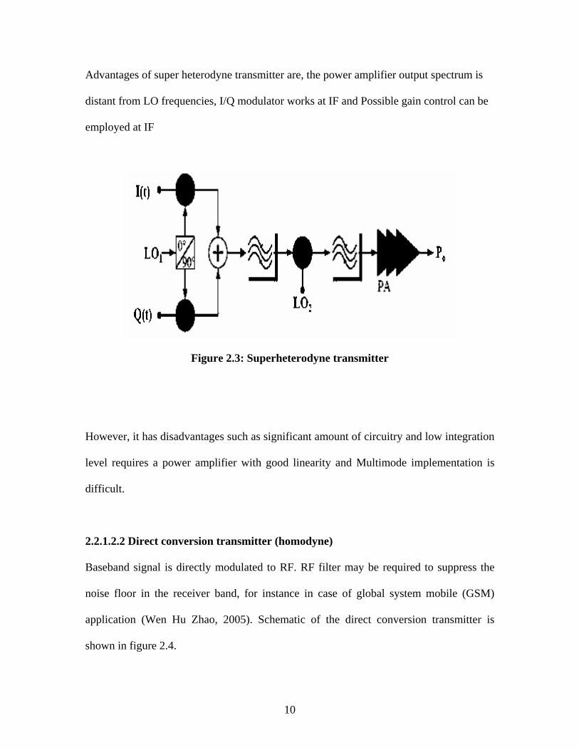
Advantages of super heterodyne transmitter are, the power amplifier output spectrum is
distant from LO frequencies, I/Q modulator works at IF and Possible gain control can be
employed at IF
Figure 2.3: Superheterodyne transmitter
However, it has disadvantages such as significant amount of circuitry and low integration
level requires a power amplifier with good linearity and Multimode implementation is
difficult.
2.2.1.2.2 Direct conversion transmitter (homodyne)
Baseband signal is directly modulated to RF. RF filter may be required to suppress the
noise floor in the receiver band, for instance in case of global system mobile (GSM)
application (Wen Hu Zhao, 2005). Schematic of the direct conversion transmitter is
shown in figure 2.4.
10
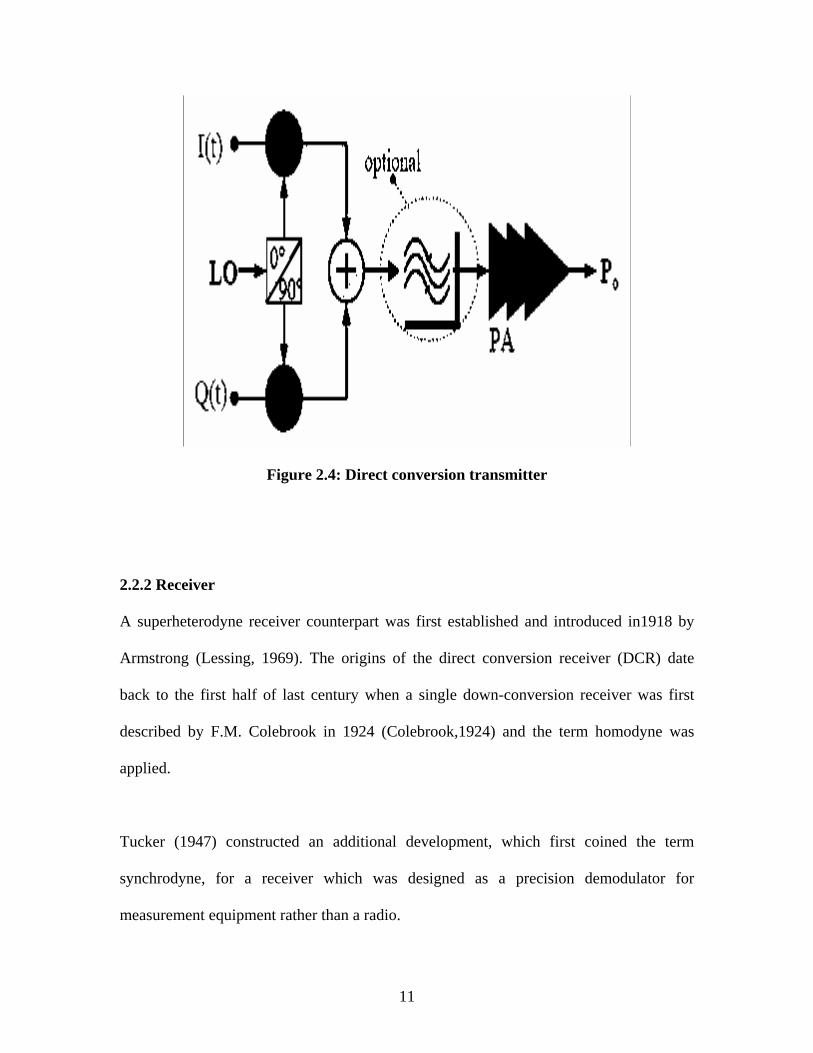
Figure 2.4: Direct conversion transmitter
2.2.2 Receiver
A superheterodyne receiver counterpart was first established and introduced in1918 by
Armstrong (Lessing, 1969). The origins of the direct conversion receiver (DCR) date
back to the first half of last century when a single down-conversion receiver was first
described by F.M. Colebrook in 1924 (Colebrook,1924) and the term homodyne was
applied.
Tucker (1947) constructed an additional development, which first coined the term
synchrodyne, for a receiver which was designed as a precision demodulator for
measurement equipment rather than a radio.
11

Tucker in (1954) reports the various single down-conversion receivers published at the
time and clarifies the difference between the homodyne (sometimes referred to as
coherent detector) and the synchrodyne receivers. The homodyne receiver obtains the LO
directly (from the transmitter, for example), whereas the synchrodyne receiver
synchronizes a free-running LO to the incoming carrier.
Over the last decade or so, the drive of the wireless market and enabling monolithic
integration technology has triggered research activities on direct conversion receivers.
These direct conversion receivers integrated with the remaining analog and digital
sections of the transceiver, have the potential to reach the "one-chip radio" goals.
Moreover, it favors multi-mode, multi-standard applications and thereby constitutes
another step towards software radio.
The present section refers to several recent publications (Abid, 1995) (Razavi, 1998)
which provide a thorough survey and insight, and display renewed interest in direct
conversion receivers. Overcoming some of the problems associated with the traditional
superheterodyne and being more prone to integration, DCR has however an array of
inherent challenges. After a brief description of alternative and well-established receiver
architectures, this article presents the direct conversion reception technique and
highlights some of the system level issues associated with DCR.
12
2.2.2.1 Quadrature signals imbalance
In MIMO-OFDM receiver systems gain and phase imbalance between I and Q channels
is another source of impairment. The sources of this type of imbalance are usually the
demodulator, amplifiers, mixer, analog to digital converter and the filters in each of the I
and Q channels. A gain imbalance result in a constellation with an oval shape and a phase
imbalance transforms the two-level signal into a multi-level signal, depending on the
amount of imbalance.
Jian Lin and Tsui (2004) suggested an adaptive scheme to correct the IQ imbalances at
the far-away transmitter as well as the receiver. Based on their model, an Adaptive IQ
imbalance improvement approach was obtained which implemented frequency domain
adaptive equalization. The approximation could result rapid converge on the order of
microseconds to rectify both constant and frequency dependent IQ imbalances and to
correct for transmitter IQ imbalance.
Tsui and Jian Lin (2004) introduced novel IQ imbalance correction approximation which
implemented frequency domain adaptive equalization. The approximation could rectify
both constant and frequency dependent IQ imbalances. It had a good appearance even
under degraded channel correction.
13

Tarighat, and Sayed (2005) studied the outcome of IQ imbalances on MIMO-OFDM
systems, and a structure for fighting such deformities through digital signal processing
was developed. An input–output relation governing MIMO OFDM systems was obtained.
The structure was used to model receiver algorithms with compensation for IQ
imbalances.
Kamata et al. (2005) announced a new extended channel matrix involving the effect of IQ
imbalance. It was verified by the personal computer simulation that the proposed
compensation method could reduce the inter-sub carrier and inter-stream interferences.
Oostveen et al. (2006) introduced an iterative algorithm for IQ imbalance compensation
in a packet-based MIMO-OFDM system with a preamble in a frequency selective fading
channel. The approach was based on iteratively estimating, in baseband at the receiver,
the receiver IQ imbalance, channel frequency response, transmitter IQ imbalance and
transmitted data.
2.2.2.2 Receiver types
Various architectures of receivers have been proposed in literature, but most popular
architectures among them are described as follows:
2.2.2.2.1 Super heterodyne Receiver
14

Super-heterodyne architecture was invented by Armstrong in 1917 and is the most widely
used architecture in wireless transceivers so far. It is dual conversion architecture in
which, at the first stage RF is down-converted to IF and then in second stage, from IF to
baseband signal (Qizheng, 2006). The block diagram of super-heterodyne receiver
architecture is shown in Figure 2.5.
Figure 2.5: Super heterodyne Receiver
From the incoming RF signal preselecting filter removes out of band signal energy as
well as partially reject image band signals. It is then amplified by LNA to suppress the
contribution of noise from the succeeding stages. Image Reject filter attenuates the
signals at image band frequencies coming from LNA. Mixer-I down converts the signal
coming out of the IR filter from RF frequency to IF frequency with the output of a Local
Oscillator. The channel selection is normally achieved through IF filter: It is a band pass
filter to allow the IF band of interest and other band is rejected. This filter is critical in
determining the sensitivity and selectivity of a receiver. Since channel selection is done at
IF, the LO requires an external tank for good phase noise performance. In case of phases
15

or frequency modulation, down conversion to the baseband requires both in-phase (I) and
quadrature (Q) components of the signal. The second down conversion of IF signal divide
it into, I and Q components for digital signal processing. The low pass filter acts as a
channel reject filter along with jobs of anti-aliasing functionality.
2.2.2.2.2 Direct Conversion Receiver (Homodyne) A simple way to reduce the number of components in the receiver and alleviate the
problem of receiver complexity is to avoid the use of intermediate frequency stage and
use complex or quadrature down conversion of the desired channel signal from RF
directly to baseband. Complete elimination of the IF stage results in highly simplified
structure where most of the channel selectivity and amplification are implemented at
baseband. On one hand, since most of the signal processing tasks takes place at low
frequencies, the power consumption is minimized. On the other hand, very low noise
operation is called for in all the remaining analog components since the amplification
provided by the RF stage is only moderate (Mohajer et al, 2007). Homodyne Direct-
Conversion Receiver is shown in figure 2. 6.
For a satisfactory receiver performance, some compensation of the DC offsets is needed.
The DC offset compensation is rather difficult to implement without compromising with
the receiver RF performance. Another analog RF related problem is that higher linearity
is required for the components because in a direct-conversion receiver, second-order.
16

Figure 2.6: Direct-Conversion Receiver
Inter modulation products may fall in the signal band, in super heterodynes, the weaker
third-order inter modulation products set the linearity requirements. These problems have
limited the use of direct-conversion principle in practical systems earlier, but nowadays
this approach is widely utilized in mobile terminals.
2.2.2.2.3 Low-IF Receiver
In Low-IF receiver architecture all the RF signals are translated to low-IF frequency
which is then down-converted to BB signal in digital domain. Low-IF architecture
comprises the advantages of both heterodyne and homodyne receivers. The block
diagram of Low-IF receiver architecture is shown in Figure2.7.
After pre selection filtering and amplification, all the RF channels are quadrature mixed
and down converted to low IF containing both wanted and unwanted signals. The IF
17

frequency is just one or two channels bandwidth away from DC, which is just enough to
overcome DC offset problems.
Figure 2.7: Low-IF Receiver
It is then amplified and filtered before sampled by ADC. Since the ADC samples have
both wanted and unwanted signals, there will be higher demand on ADC dynamic range
requirements. The ac-coupled signal path to ADC eliminates the need of DC offset
compensation circuitry. The sampled digital data are fed to image reject mixer which is
implemented in digital domain (Chung-Yun et al, 2002).
2.2.2.2.4 Wideband IF receiver
18

Wideband-IF receiver is dual conversion architecture in which data is down converted
from RF to IF in the 1st stage, and in the 2nd stage it is from IF to Baseband. The block
diagram of Wideband-IF receiver architecture is shown in Figure 2.8.
Figure 2.8: Wideband IF receiver
In this architecture all the RF channels are complex mixed and down converted to fix IF
after pre selection filtering and amplification. In second stage an Image Reject (IR) mixer
does complex mixing and translate IF to BB using a tunable channel select frequency
synthesizer. All the image frequencies are canceled by IR mixer. If the IF is chosen high
enough, additional image rejection may be obtained from the RF front-end pre selection
filter. Channel selection is performed at baseband by using programmable integrated
channel select filter. Since LO-1 is fixed, frequency synthesizer generated by crystal
controlled oscillator good phase noise performance is obtained. Channel tuning is
achieved by using programmable frequency synthesizer at IF (Richter et al, 2003).
19

2.2.3 Receiver Specification
Receiver Specification can be listed as shown below:
• Receiver sensitivity
• Receiver selectivity
2.2.3.1 Receiver sensitivity
The Minimum Detectable Signal (MDS) power Pi (min) at which a receiver can detect a
signal while providing an adequate SNRo (min) at analog receiver output or BER at
digital receiver output, for demodulation is called receiver sensitivity. The maximum
BER dictates the minimum output SNR (SNRo (min)) necessary for satisfactory
reproduction of the desired signal. The relation between SNR and BER is given by:
dBBRdBNoEbdBSNRo )/()/()( += (2 .1)
where,
R - Bit rate
B - Channel Bandwidth
Eb - Energy per bit
SNR at the input, SNRin is determined by input signal power (Pin) and noise floor
(NFloor).
)()()( dBmNFloordBmPindBSNRin −= (2.2)
20

)log(10/174 BHzdBmNFloor +−= (2.3)
After determining the minimum SNR required at the output of receiver from top level
simulation, and knowing the SNR at the input, NF of the receiver can be determined.
)(min)()()( dBSNRodBSNRindBNFRx −=
dBBRdBNoEbBHzdBmdBPin )/()/()log(10)/(174)( +−−+= (2.4)
If Pin = Pi (min), then sensitivity is given as,
)(min)()()log(10/174)(min)( dBSNRdBNFRxBHzdBmdBmPin +++− (2.5)
2.2.3.2 Receiver selectivity
The ability of a receiver to extract the desired signal in the presence of strong adjacent
frequency interferers and channel blockers. Selectivity is determined by SSB phase noise,
synthesizer spurs, IF selectivity, IF band width and co-channel rejection.
• Selectivity of the adjacent and alternate channels.
• Selectivity of interferences to inter modulation of third order.
• Blocking interferences selectivity.
• Selectivity is critical for good intermodulation performance.
21
2.2.3 Communication channel
The term channel, in communications, refers to the medium used to carry information
from a transmitter to a receiver. Many types of channels are used in communication
systems including wire conductors, fiber-optic, and free space.
2.2.3.1 Cables
A cable is one or more wires bound together, typically in a common protective jacket.
The individual wires inside the jacket may be covered up or isolated. Combining cables
may comprise both electrical wires. Electrical wire is usually copper due to its excellent
conductivity, but aluminum is sometimes used since it costs less.
2.2.3.2 Fiber optic
An optical fiber is a glass or plastic fiber that takes light along its length. Fiber optics is a
branch of applied science and engineering, concerned with the purpose and application
program of optical fibers. Optical fibers are widely used in fiber optic communication,
which allow transmission over longer distances and at higher data rates than other forms
of communications. Fibers are used rather than metal wires because signals follow them
with less loss, and they are resistant to electromagnetic disturbance. Optical fibers are
also used to form sensors, and in a kind of other practical application. Light is kept in the
22
core of the optical fiber by number of inner reflection. This causes the fiber to act as a
waveguide (Udd, 1996).
2.2.3.3 Free space
In classical physics, free space is a term of electromagnetic theory, representing a
theoretically perfect vacuum, and sometimes related to the vacuum of free space. Radio is
the universal term used to any kind of electromagnetic spectrum data signal are
convinced to electric and magnetic fields that spread through space over long distance
(John et al, 2005).
Summary
In this chapter, the basic concept of several kinds of transmitters and receivers has been
reviewed, describing the previous researches at each stage. The focus of the review was
mainly on Direct Conversion Transmitter and Direct Conversion Receiver. Direct
conversion transmitter power linearization techniques were reviewed. Furthermore,
several quadrature signal imbalance methods were shown. In addition, the main idea of
MIMO-OFDM concept is also being discussed.
23

CHAPTER THREE
MIMO WIRELESS TRANSCEIVER DESIGN
3.1 Introduction This chapter deals with the design and fabrication procedure required for RF MIMO
transceiver. The transceiver consists of the following four major parts:
1. Digital to analog converter
2. Analog to digital converter
3. Transmitter and
4. Receiver
The transmitter consists of two parts: the IQ modulator and the power amplifier .The
receiver consists of two parts: the low noise amplifier and the demodulator. The design
process flow can be illustrated by the flow chart as shown in Figure 3.1; the chart
highlights the stages through which the transceiver has been developed.
3.2 Simulation and fabrication software
In the present study separate softwares were used for simulation and printed a circuit
board (PCB) fabrication. For simulation part Agilent Advanced design system” ADS”
was used and for PCB fabrication Orcad software was used.
24