universiti putra malaysia - connecting repositories · dalam kajian ini, siri (cdse)1-x(se)x dan...
TRANSCRIPT

.
UNIVERSITI PUTRA MALAYSIA
ELECTRICAL AND THERMAL PROPERTIES OF THE COMPOSITE SEMICONDUCTORS, (CdSe)1-x(Se)x AND (CdS)1-x(S)x
NUR AMALINA MUSTAFFA
FS 2008 43
ELECTRICAL AND THERMAL PROPERTIES OF THE COMPOSITE SEMICONDUCTORS, (CdSe)1-x(Se)x AND (CdS)1-x(S)x
By
NUR AMALINA MUSTAFFA
Thesis Submitted to the School of Graduate Study, Universiti Putra Malaysia, in Fulfilment of the Requirements for the Degree of Master of Science
October 2008

ii
DEDICATION
Specially Dedicated to My Beloved Family,
Mustaffa Tupir Mohamed & Che Norlia Abdullah
Mohd. Taufiq Mustaffa
Amal Nabilah Mustaffa
Amal Aqilah Mustaffa
and to My Beloved ONE,
Muhammad Naguib Thasleem Mohd.
for their unconditional support, inspiration, patience and love.
iii
Abstract of thesis submitted to the Senate of Universiti Putra Malaysia in fulfilment of the requirements for the Degree of Master of Science
ELECTRICAL AND THERMAL PROPERTIES OF THECOMPOSITE
SEMICONDUCTORS, (CdSe)1-x(Se)x AND (CdS)1-x(S)x
By
NUR AMALINA MUSTAFFA
October 2008 Chairman: Associate Professor Dr. Zainal Abidin Talib, PhD Faculty : Science A series of (CdSe)1-x(Se)x and (CdS)1-x(S)x composite semiconductors were prepared
with different stoichiometric compositions of Se and S with x = 0 to x = 0.8 both in the
interval of 0.2 by varying the ratio of CdSe:Se and CdS:S in a reaction mixture. The
following powder of CdSe, Se and CdS, S were used as the starting materials.
X-ray diffraction analysis was carried out in order to investigate the structural character
of the composites obtained. For both samples, analysis of the X-ray diffractogram
revealed that the samples were in hexagonal form. Atomic Force Microscopy (AFM)
was used for analyzing the surface morphology of the composites samples.
Parallel plate method was used to determine the dc conductivity of all samples in the
temperature range of 300 – 460 K. Both samples, (CdSe)1-x(Se)x and (CdS)1-x(S)x ,
show variation in ln σ with 1000/T (K-1) that indicated that there are three distinct

iv
temperature zones with three different characteristic regions. This behaviour suggests
that two types of conduction mechanisms were presence. The first region is identified as
the extrinsic region, the second region is the intermediate region and the third region is
the intrinsic region. For both series of samples, the conductivity obtained for all series
of samples shown similar trend, the dc conductivity increased as the temperature
increased. For (CdSe)1-x(Se)x composite where x = 0, the dc conductivity at 300 K is
about 10-8 S/cm and increase up to 10-5 S/cm at 460 K. While for (CdS)1-x(S)x composite
where x = 0, the dc conductivity at 300 K is about 10-10 S/cm and increase up to 10-8
S/cm at 503 K. The activation energies were calculated from the Arrhenius relation and
the values of the activation energy indicated that all the prepared samples were
semiconductors.
The ac conductivity properties of polycrystalline (CdSe)1-x(Se)x and (CdS)1-x(S)x were
studied in temperature range of 300 – 523 K and frequency range of 100 Hz – 1 MHz
using Impedance Analyzer. Obtained data of ac conductivity revealed that at low
frequency σAC (ω) was independent of frequency and proportional to ωs at higher
frequency for all samples. The values of the frequency exponent, s were found to
decrease with increasing temperature which suggested that the dominant transport
process as Correlated Barrier Hopping (CBH).
Thermal diffusivity values of both (CdSe)1-x(Se)x and (CdS)1-x(S)x were investigated
using photoflash technique. Thermal diffusivity value decrease as we increase the Se
and S compositions in the samples.

v
Abstrak tesis ini yang dikemukakan kepada Senat Universiti Putra Malaysia sebagai memenuhi keperluan untuk Ijazah Master Sains
SIFAT ELEKTRIK DAN PENGUKURAN PENYERAPAN TERMA BAHAN KOMPOSIT SEMIKONDUKTOR, (CdSe)1-x(Se)x DAN (CdS)1-x(S)x
Oleh
NUR AMALINA MUSTAFFA
Oktober 2008
Pengerusi : Professor Madya Dr. Zainal Abidin Talib, PhD Fakulti : Sains Dalam kajian ini, siri (CdSe)1-x(Se)x dan (CdS)1-x(S)x komposit semikondutor telah
disediakan dalam pelbagai komposisi stoichiometri Se dan S dengan x = 0 hingga x =
0.8 kedua-duanya, pada selangan sebanyak 0.2 dengan mempelbagaikan ratio CdSe :Se
dan CdS :S dalam bahan tindak balas. CdSe, Se dan CdS, S digunakan sebagai bahan
asas di dalam penyediaan sample.
Belauan sinar-X telah digunakan untuk mengenal pasti struktur bahan komposit yang
telah diperolehi. Bagi kedua-dua bahan, struktur heksagonal diperolehi daripada spektra
belauan sinar-X. Mikroskop Daya Atom (AFM) digunakan untuk mengkaji struktur
permukaan bahan komposit tersebut.
Kaedah kepingan selari telah digunakan untuk mengkaji kekonduksian dc bagi semua
bahan di dalam julat suhu 300 - 460 K. Bagi kedua-dua sample, (CdSe)1-x(Se)x dan
vi
(CdS)1-x(S)x, graf ln σ melawan 1000/T (K-1) menunjukkan, terdapat tiga zon dengan
tiga ciri yang berbeza. Ini menunjukkan terdapat dua jenis kekonduksian yang terlibat.
Zon pertama merupakan zon yang tidak tulen, zon kedua ialah zon pertengahan, dan zon
ketiga merupakan zon yang tulen. Untuk kedua-dua siri sample, didapati kekonduksian
dc meningkat apabila suhu meningkat. Bagi (CdSe)1-x(Se)x apabila x = 0, kekonduksian
dc pada suhu 300 K ialah 10-8 S/cm dan meningkat kepada 10-5 S/cm pada suhu 460 K.
Manakala bagi sample (CdS)1-x(S)x apabila x = 0 pula, kekonduksian dc meningkat dari
10-10 S/cm pada suhu 300 K ke 10-8 S/cm pada suhu 503 K. Tenaga pengaktifan telah
dikira daripada persamaan Arrhenius dan nilai-nilainya menunjukkan semua bahan yang
telah disediakan merupakan bahan semikonducktor.
Kekonduksian ac bagi bahan (CdSe)1-x(Se)x and (CdS)1-x(S)x telah dikaji di dalam julat
suhu 300 - 523 K dan julat frekuensi 100 – 1 MHz menggunakan Impedance Analyzer.
Data yang telah diperolehi menujukkan pada julat frekuensi yang rendah, σAC(ω) adalah
tidak bergantung pada frekuensi tetapi berkadaran dengan ωs pada frekuensi yang lebih
tinggi pada semua sample bahan. Nilai frekuensi exponen, s didapati menurun dengan
penurunan suhu. Ini menunjukkan proses kekonduksian di dalam bahan tesebut telah
dikenal pasti sebagai Loncatan Halangan Berkaitan (CBH).
Nilai penyerapan terma bagi kedua-dua bahan telah diperolehi daripada kaedah sinaran
flash kamera. Nilai penyerapan terma menurun dengan pertambahan Se and S di dalam
bahan tersebut.

vii
ACKONWLEDGEMENTS
First and foremost, I would like to extend my praise to Allah s.w.t that gives me the
strength, determination, patience and courage to produce this thesis.
I would like to express my special gratitude to Assoc. Prof. Dr. Zainal Abidin Talib for
all he has done for me as a research advisor. Without his assistance, guidance, ideas,
supervision and encouragement, I would not be able to complete my graduate studies at
Universiti Putra Malaysia. I would also like to extend my sincere appreciation to my co-
supervisor, Assoc. Prof. Dr. Wan Mohd. Daud Wan Yusoff for his advice and helpful
discussion during my period of study. I would also like to express my gratitude to all the
lecturers and staff in Physics Department for providing research facilities and for all
their help and cooperation given throughout my study. I gratefully acknowledge the
Academy of Sciences Malaysia and MOSTI through SAGA Grant (5486512) for their
financial support. I would also like to acknowledge Universiti Teknologi Mara and
Ministry of Higher Education for the scholarship that allows me to complete this work.
My sincere thanks to all my friends who have directly or indirectly contributed toward
the success of this study. Last but not least, to my beloved parents, siblings, relatives
and also to my beloved Naguib, I would like to extend my special thanks for their love,
understanding, support, patience and encouragement. Without them, the path to this
thesis will be a lonely endeavor. Your love and belief have given me strength to walk
through difficulties to achieve success.

viii
I certify that an Examination Committee met on 14th October 2008 to conduct the final examination of Nur Amalina Mustaffa on her Master of Science thesis entitled “Electrical and Thermal Properties of the Composite Semiconductors, (CdSe)1-x(Se)x and (CdS)1-x(S)x” in accordance with Universiti Pertanian Malaysia (Higher Degree) Regulations 1981. The committee recommends that the candidate be awarded the relevant degree. Members of the examination committee are as follows: Zaidan Abdul Wahab, PhD Associate Professor Faculty of Science Universiti Putra Malaysia (Chairperson) Senin Hassan, PhD Professor Faculty of Science and Technology Universiti Malaysia Terengganu (External Examiner) Wan Mahmood Mat Yunus, PhD Professor Faculty of Science Universiti Putra Malaysia (Internal Examiner) Abdul Halim Shaari, PhD Professor Faculty of Science Universiti Putra Malaysia (Internal Examiner) Hasanah Mohd. Ghazali, PhD Professor and Dean School of Graduate Studies Universiti Putra Malaysia Date: 30th December 2008

ix
This thesis was submitted to the Senate of Universiti Putra Malaysia and has been accepted as partial fulfilment of the requirements for the Degree of Master of Science. The members of the Supervisory Committee are as follows: Zainal Abidin Talib, PhD Associate Professor Faculty of Science Universiti Putra Malaysia (Chairman) Wan Mohd. Daud Wan Yusoff, PhD Associate Professor Faculty of Science Universiti Putra Malaysia (Member)
Hasanah Mohd. Ghazali, PhD Professor and Dean School of Graduate Studies Universiti Putra Malaysia
Date: 15th January 2009

x
DECLARATION
I hereby declare that the thesis is based on my original work except for quotations and citations which have been fully acknowledged. I also declare that it has not been previously or concurrently submitted for any other degree at UPM or other institutions.
NUR AMALINA MUSTAFFA
Date:

xi
TABLE OF CONTENTS
PAGE
DEDICATION ii ABSTRACT iii ABSTRAK v ACKNOWLEDGEMENTS vii APPROVAL viii DECLARATION x LIST OF TABLES xiv LIST OF FIGURES xv LIST OF ABBREVIATION xix LIST OF SYMBOLS xx CHAPTER 1 INTRODUCTION 1.1 Introduction 1 1.2 II-VI Semiconductor 3 1.3 Cadmium Selenide, CdSe 4 1.4 Cadmium Sulphide, CdS 5 1.5 Electrical Properties 7 1.5.1 Electrical Resistivity and Conductivity 7 1.6 Thermal Properties 8 1.6.1 Thermal Diffusivity 8 1.7 The Objective of Study 10 2 LITERATURE REVIEW
2.1 Introduction 11 2.2 Brief Literature on CdSe and (CdSe)1-x(Se)x 11 2.2.1 Structural Properties 12 2.2.2 Electrical Properties 14 2.3 Brief Literature on CdS and (CdS)1-x(S)x 18 2.3.1 Structural Properties 18 2.3.2 Electrical Properties 20 2.4 Measurement of Thermal Diffusivity using
Photoflash Technique 24
xii
3 THEORY 3.1 Semiconductor Materials 26 3.2 Compound Semiconductor 27 3.3 Electrical Conductivity 29 3.4 Charge Carriers and Energy Level in Semiconductor 32 3.5 Drift and Diffusions Current 35 3.6 Conductivity and Resistivity 36 3.7 Intrinsic Semiconductors 37 3.8 Extrinsic Semiconductors 37 3.9 Correlated Barrier Hopping 38 3.10 Thermal Properties 43 3.11 Photoflash technique 43
4 METHODOLOGY
4.1 Samples Preparation 46 4.2 X-Ray Diffraction (XRD) Analysis 49 4.3 Microstructure Analysis 51 4.4 DC Conductivity Measurements 52 4.5 AC Conductivity Measurements 53 4.6 Photoflash Technique 55
4.6.1 Experimental Procedure of Photoflash Technique 57
5 RESULTS AND DISCUSSION 5.1 Introduction 58 5.2 X-Ray Diffraction (XRD) Analysis 59 5.3 Microstructure Analysis 62 5.4 Electrical Properties of (CdSe)1-x(Se)x and (CdS)1-x(S)x 65 5.4.1 The Effect of Temperature on the Dc Conductivity of 65
(CdSe)1-x(Se)x and (CdS)1-x(S)x 5.4.2 The Effect of Se and S Compositions on the 82
Dc Conductivity of (CdSe)1-x(Se)x and (CdS)1-x(S)x 5.4.3 The Effect of Temperature on the Ac Conductivity of 85
(CdSe)1-x(Se)x and (CdS)1-x(S)x 5.4.4 The Effect of Se and S Compositions on the 99
Ac Conductivity of (CdSe)1-x(Se)x and (CdS)1-x(S)x 5.4 Thermal Diffusivity of (CdSe)1-x(Se)x and (CdS)1-x(S)x 104 6 CONCLUSION AND SUGGESTION
6.1 Conclusion 107 6.2 Suggestion for Future Work 110

xiii
REFERENCES 111 APPENDICES 115 BIODATA OF THE STUDENT 116

xiv
LIST OF TABLES
Table
Page
1.1 Semiconductor crystalline structure
4
5.1 Activation energies values for (CdSe)1-x(Se)x , (x = 0,0.2,0.4,0.5, 0.6,0.8)
77
5.2 Activation energies values for (CdS)1-x(S)x , (x = 0,0.2,0.4,0.5, 0.6,0.8)
82
5.3 The binding energy, WM for samples with various concentration of x, Se x for (CdSe)1-x(Se)x
96
5.4 The binding energy, WM for samples with various concentration of x, S x for (CdS)1-x(S)x
98

xv
LIST OF FIGURES Figure
Page
1.1 Crystalline structures of the a) diamond and zinc blende (cubic) and b) wurzite (hexagonal) semiconductors
3
1.2 Crystalline structures of CdSe
5
1.3 Crystalline structures of CdS
6
3.1 Classifications of material
26
3.2 Elements found in elemental and compound semiconductors
28
3.3 Compound II-VI semiconductors, CdSe
28
3.4 Electrical conductivities of some common materials
30
3.5 The energy bands of insulator, semiconductor and conductor
31
3.6 Energy level diagrams of a semiconductor
33
3.7 Model of overlapping Coulomb-type wells for charged centers
40
3.8 Schematic diagram of the hopping process for bipolarons in amorphous chalcogenide
41
3.9 Schematic diagram of the hopping process for single polarons in amorphous chalcogenide
41
3.10 Schematic diagram of the flash method 44
3.11 Temperature increase for various experimental conditions
45
4.1 Flow chart for sample preparation
48
4.2 Schematic representations of reflection of x-ray in crystalline material
50
4.3 Basic block diagram of an AFM
51
4.4 Schematic diagram for two probe system
52

xvi
4.5 Connections of the Novotherm units and the sample cell 54
4.6 Schematic diagram of the photoflash technique 55
5.1 X-Ray Diffraction Pattern of (CdSe)1-x(Se)x 60
5.2 X-Ray Diffraction Pattern of (CdS)1-x(S)x
62
5.3 The surface morphology of (CdSe)1-x(Se)x (a) x=0 (b) x=0.2 (c) x=0.4 (d) x=0.5 (e) x=0.6 (f) x=0.8 obtained from AFM
63
5.4 The surface morphology of (CdS)1-x(S)x (a) x=0 (b) x=0.2 (c) x=0.4 (d) x=0.5 (e) x=0.6 (f) x=0.8 obtained from AFM
64
5.5 I-V characteristic of (CdSe)1-x(Se)x with x = 0
66
5.6 I-V characteristic of (CdSe)1-x(Se)x with x = 0.2
67
5.7 I-V characteristic of (CdSe)1-x(Se)x with x = 0.4
67
5.8 I-V characteristic of (CdSe)1-x(Se)x with x = 0.5
68
5.9 I-V characteristic of (CdSe)1-x(Se)x with x = 0.6
68
5.10 I-V characteristic of (CdSe)1-x(Se)x with x = 0.8
69
5.11 I-V characteristic of (CdS)1-x(S)x with x = 0
70
5.12 I-V characteristic of (CdS)1-x(S)x with x = 0.2
70
5.13 I-V characteristic of (CdS)1-x(S)x with x = 0.4
71
5.14 I-V characteristic of (CdS)1-x(S)x with x = 0.5
71
5.15 I-V characteristic of (CdS)1-x(S)x with x = 0.6
72
5.16 I-V characteristic of (CdS)1-x(S)x with x = 0.8
72
5.17 Arhenius plot of (CdSe)1-x(Se)x with x = 0 , solid line represent the best fitted value for activation energy
74
5.18 Arhenius plot of (CdSe)1-x(Se)x with x = 0.2 solid line represent the best fitted value for activation energy
75
5.19 Arhenius plot of (CdSe)1-x(Se)x with x = 0.4 solid line represent the best fitted value for activation energy
75

xvii
5.20 Arhenius plot of (CdSe)1-x(Se)x with x = 0.5 solid line represent the best fitted value for activation energy
76
5.21 Arhenius plot of (CdSe)1-x(Se)x with x = 0.6 Solid line represent the best fitted value for activation energy
76
5.22 Arhenius plot of (CdSe)1-x(Se)x with x = 0.8 Solid line represent the best fitted value for activation energy
77
5.23 Arhenius plot of (CdS)1-x(S)x with x = 0 , solid line represent the best fitted value for activation energy
79
5.24 Arhenius plot of (CdS)1-x(S)x with x = 0.2 solid line represent the best fitted value for activation energy
79
5.25 Arhenius plot of (CdS)1-x(S)x with x = 0.4 solid line represent the best fitted value for activation energy
80
5.26 Arhenius plot of (CdS)1-x(S)x with x = 0.5 solid line represent the best fitted value for activation energy
80
5.27 Arhenius plot of (CdS)1-x(S)x with x = 0.6 solid line represent the best fitted value for activation energy
81
5.28 Arhenius plot of (CdS)1-x(S)x with x = 0.8 solid line represent the best fitted value for activation energy
81
5.29 Dc conductivity of (CdSe)1-x(Se)x with different Se concentration
83
5.30 Dc conductivity of (CdS)1-x(S)x with different Se concentration
84
5.31 Frequency dependence of σAC (f) for (CdSe)1-x(Se)x with x= 0 88
5.32 Frequency dependence of σAC (f) for (CdSe)1-x(Se)x with x= 0.2
88
5.33 Frequency dependence of σAC (f) for (CdSe)1-x(Se)x with x= 0.4
89
5.34 Frequency dependence of σAC (f) for (CdSe)1-x(Se)x with x= 0.5
89
5.35 Frequency dependence of σAC (f) for (CdSe)1-x(Se)x with x= 0.6
90
5.36 Frequency dependence of σAC (f) for (CdSe)1-x(Se)x with x= 0.8
90
5.37 Frequency dependence of σAC (f) for (CdS)1-x(S)x with x= 0
92
5.38 Frequency dependence of σAC (f) for (CdS)1-x(S)x with x= 0.2 92

xviii
5.39 Frequency dependence of σAC (f) for (CdS)1-x(S)x with x= 0.4
93
5.40 Frequency dependence of σAC (f) for (CdS)1-x(S)x with x= 0.5 93
5.41 Frequency dependence of σAC (f) for (CdS)1-x(S)x with x= 0.6
94
5.42 Frequency dependence of σAC (f) for (CdS)1-x(S)x with x= 0.8
94
5.43 Parameter of s with different Se compositions for (CdSe)1-x(Se)x
97
5.44 Parameter of 1-s with different Se compositions for (CdSe)1-
x(Se)x
97
5.45 Parameter of s with different S compositions
98
5.46 Parameter of 1-s with different S compositions
99
5.47 AC Conductivity of (CdSe)1-x (Se)x , x = 0.2 – 0.8 at 100 Hz
101
5.48 AC Conductivity of (CdSe)1-x (Se)x , x = 0.2 – 0.8 at 1 kHz
101
5.49 AC Conductivity of (CdS)1-x (S)x , x = 0.2 – 0.8 at 100 Hz
103
5.50 AC Conductivity of (CdS)1-x (S)x , x = 0.2 – 0.8 at 1 kHz
103
5.51 Thermal diffusivity value of (CdSe)1-x(Se)x with different Se concentration
106
5.52 Thermal diffusivity value of (CdS)1-x(S)x with different S Concentration
106
xix
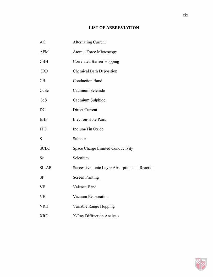
LIST OF ABBREVIATION
AC Alternating Current
AFM Atomic Force Microscopy
CBH Correlated Barrier Hopping
CBD Chemical Bath Deposition
CB Conduction Band
CdSe Cadmium Selenide
CdS Cadmium Sulphide
DC Direct Current
EHP Electron-Hole Pairs
ITO Indium-Tin Oxide
S Sulphur
SCLC Space Charge Limited Conductivity
Se Selenium
SILAR Successive Ionic Layer Absorption and Reaction
SP Screen Printing
VB Valence Band
VE Vacuum Evaporation
VRH Variable Range Hopping
XRD X-Ray Diffraction Analysis

xx
LIST OF SYSMBOLS
ρ Resistivity
σ Electrical Conductivity
I Current though the object
V Potential difference across the object
R Resistance of an object
L Thickness of the pellet sample
A Cross sectional area of the object
n Number of the charge carriers in the material
q The charge carrier by each carrier
μ Mobility of the carrier
ω Angular frequency
Eg Energy gap
E Electric field
Wm Maximum barrier height
s Frequency exponent
kB
Boltzmann constant
τo Characteristic relaxation time
WH Effective barrier height
α Thermal Diffusivity
t0.5
Time to reach 50% of the maximum
G Conductance

CHAPTER I
INTRODUCTION
1.1 Introduction The phenomenal growth in research effort devoted to the study of semiconductor, whose
conductivity lies between a conductor and an insulator, during the past two decades has
resulted in a very large literature on the subject. The first feature used to distinguish
semiconductors from electrical conductors was their negative temperature coefficient of
resistance which their resistance generally falls as the temperature is raised. This effect
has been first notice by Michael Faraday when carrying his experiments on silver
sulphide (Smith, 1978).
II-VI compound semiconductors and their alloys have been the subject of extensive
research for several decades in both fundamental studies and device applications. The
broad range of band gaps and lattice constants, the highly polar nature of these materials
and the possibility of incorporating magnetic ions isoelectronically have been key
factors that distinguish II-VI materials from their III-V counterparts. Because of this, II-
VI semiconductors are particularly attractive for a wide range of applications such as
infrared lasers and detectors, blue-green lasers and light emitting diodes (LEDs),
nonlinear optical materials, magneto-optical devices and radiation detectors. Such
applications have significantly improved photonics, computers, telecommunications as
well as many other industries and technologies.

2
Nevertheless, during 1960s and 1970s II-VI materials did not receive much attention
from the semiconductor community due to limitations of growth and doping techniques.
Only in the 1980s and 1990s, with the advent of advanced crystal growth techniques
such as metal-organic chemical vapor deposition (MOCVD) and molecular beam
epitaxy (MBE), did a new surge of research devoted to II-VIs emerge. Presently, with
progress along many new directions, including spintronics, nonlinear optical devices
and, especially, quantum heterostructures, II-VI materials are beginning to be looked at
again.
Among the II-VI materials, Cadmium Selenide (CdSe) and Cadmium Sulphide (CdS)
are of great interest because of their potential in many practical applications such as
solar cells, optical detectors, field-effect transistors, dosimeters of ionized radiation and
optoelectronics devices. CdSe and CdS are very promising for solar cells because of
their suitable direct band gap as the band gap for CdS is 2.4 eV ( Prabahar and Dhanam,
2005) at 300 K and CdSe is 1.74 eV (Shreekanthan et al. 2003) at 300 K. Furthermore,
their optical absorption and good stability also make them ideal and suitable as a
medium for solar cells.

3
1.2 II-VI Semiconductor
For the last five decades, a huge number of research activities have been devoted to the
studies of the crystalline structure of binary semiconductor materials, resulting in the
fact that this physical property has been well known and documented. Among the types
of the crystalline structure, diamond, zinc blende and wurzite are common ones and the
semiconductors possessing these structures are of interest for device applications.
Depending on growth conditions, one can obtain both the cubic (diamond, zinc blende)
and the hexagonal (wurzite) structures for most of II-VI binaries. These crystalline
structures are illustrated in Fig.1.1 below.
Figure 1.1: Crystalline structures of the a) diamond and zinc blende
(cubic) and b) wurzite (hexagonal) semiconductors
4
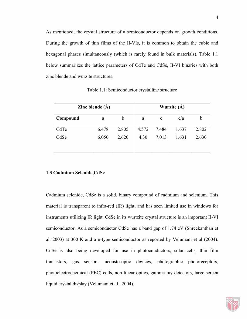
As mentioned, the crystal structure of a semiconductor depends on growth conditions.
During the growth of thin films of the II-VIs, it is common to obtain the cubic and
hexagonal phases simultaneously (which is rarely found in bulk materials). Table 1.1
below summarizes the lattice parameters of CdTe and CdSe, II-VI binaries with both
zinc blende and wurzite structures.
Table 1.1: Semiconductor crystalline structure
Zinc blende (Å) Wurzite (Å)
Compound a b a c c/a b
CdTe
CdSe
6.478
6.050
2.805
2.620
4.572
4.30
7.484
7.013
1.637
1.631
2.802
2.630
1.3 Cadmium Selenide,CdSe
Cadmium selenide, CdSe is a solid, binary compound of cadmium and selenium. This
material is transparent to infra-red (IR) light, and has seen limited use in windows for
instruments utilizing IR light. CdSe in its wurtzite crystal structure is an important II-VI
semiconductor. As a semiconductor CdSe has a band gap of 1.74 eV (Shreekanthan et
al. 2003) at 300 K and a n-type semiconductor as reported by Velumani et al (2004).
CdSe is also being developed for use in photoconductors, solar cells, thin film
transistors, gas sensors, acousto-optic devices, photographic photoreceptors,
photoelectrochemical (PEC) cells, non-linear optics, gamma-ray detectors, large-screen
liquid crystal display (Velumani et al., 2004).