universitat politecnica de val` encia`
TRANSCRIPT

UNIVERSITAT POLITECNICA DE VALENCIA
DEPARTAMENT DE COMUNICACIONS
Apodized Coupled Resonator Optical
Waveguides: Theory, design andcharacterization
Ph.D. THESIS
byJose David Domenech Gomez
Valencia, July 2013


UNIVERSITAT POLITECNICA DE VALENCIA
DEPARTAMENT DE COMUNICACIONS
Apodized Coupled Resonator Optical
Waveguides: Theory, design andcharacterization
Jose David Domenech GomezOptical and Quantum Communications Group.
iTEAM Research InstituteUniversitat Politecnica de Valencia.
Camı de Vera s/n, 46022 Valencia, [email protected]
Ph.D. Supervisors:Dr. Pascual Munoz Munoz
Prof. Jose Capmany Francoy
Valencia, July 2013

2

To my family and friends.In loving memory of Basilio.


La verdadera ciencia ensena,sobre todo, a dudar y a ser ignorante.
Ernest Rutherford


Agradecimientos
En primer lugar mis agradecimientos van dirigidos al grupo de investigacion enel que he realizado esta tesis doctoral. El grupo de comunicaciones opticas ycuanticas de la Universidad Politecnica de Valencia. En este grupo no solo heconocido a grandes profesionales sino a grandes personas y amigos. Tambien quer-ria dar las gracias a mi co-director de tesis y director del grupo de investigacionel catedratico Jose Capmany por la oportunidad que me ha brindado de formarparte de tan prestigioso grupo ası como por su apoyo durante la realizacion deesta tesis.
Un agradecimiento muy especial va dirigido a la persona que me introdujo en elmundo de las comunicaciones opticas alla por el ano 2006, el Dr. Pascual Munoz.El ha sido director y en gran parte responsable de todos mis logros academicos,desde el proyecto final de carrera, la tesina de master hasta finalmente esta tesisdoctoral. Para mi no solo ha sido un mentor en el ambito profesional sino que alo largo de los anos tambien se ha convertido en un amigo mas.
No querrıa dejar de agradecer tambien a toda mi familia por el apoyo que mehan prestado a lo largo de todos estos anos. A mis padres, hermanos, tios, primos,que siempre creyeron en mi y me lo demostraron dıa tras dıa. Por supuestotambien he de agradecer a todos los amigos que me animaron a continuar conla investigacion aunque a muchos de ellos no les quedara nunca claro a que mededicaba en la universidad. Por ultimo querrıa agradecer muy especialmente a mimujer Alicia ya que sin ella nada de esto habrıa sido posible. Ademas de estaral pie del canon durante todo este tiempo me ha dado lo mas grande que me hapasado en toda mi vida: nuestro hijo David.


Abstract
In this thesis we propose the apodization or windowing of the coupling coefficientsof the unit cells conforming a coupled resonator device as a mean to improve thespectral response of these filters. In the same way, we have developed a synthesisalgorithm for CROW devices, that given an objective response yields the couplingconstants for every resonator within the array. We also have introduced a noveltechnique for the apodization of coupled resonator structures by applying a lon-gitudinal offset between resonators in order to set the appropriate power couplingconstant for obtaining a targeted response, which alleviates the technical require-ments required for the production of these devices. We have demonstrated thedesign, fabrication and characterization of CROW structures employing the apo-dization through the aforementioned technique in Silicon-On-Insulator technologyand validated the theoretical predictions. Lastly, we have explored the delay andphase characteristics of CROW devices and introduced a novel architecture formicrowave signal processing in beamforming networks employing resonators asphase-shifting sections.


Resumen
En esta tesis, proponemos la apodizacion o enventanado de los coeficientes deacoplo de cada uno de los resonadores que conforman los dispositivos de multiplescavidades resonantes acopladas con tal de reducir el nivel de los lobulos secun-darios en el caso de la configuracion SCISSOR o el rizado en la banda pasante,presente en la configuracion CROW. De la misma manera, hemos desarrolladoun algoritmo de sintesis de dispositivos CROW en el que, dada una respuestaobjetivo, obtenemos las constantes de acoplo necesarias para cada resonador deldispositivo. Tambien hemos introducido una tecnica novel para implementar laapodizacion de estructuras basadas en anillos resonantes acoplados mediante laaplicacion de un offset longitudinal entre los resonadores con tal de modificar lascontantes de acoplo de las cavidades, lo cual alivia los requerimientos tecnicospara la fabricacion de estos dispositivos. Hemos demostrado el diseno, fabricaciony caracterizacion de estructuras CROW empleando la apodizacion a traves de latecnica mencionada anteriormente en tecnologia de Silicon-On-Insulator (SOI) yvalidado las predicciones teoricas. Por ultimo, hemos explorado las caracterısticasde retardo y fase de los dispositivos CROW e introducido una nueva arquitecturapara el procesamiento de senales de microondas en redes de conformado de hazempleando resonadores como elementos desfasadores.


Resum
En aquesta tesi, proposem l’apoditzacio dels coeficients d’acoble de cada un delsressonadors que conformen els dispositius de multiples cavitats ressonants acobladesamb tal de reduir el nivell dels lobuls secundaris en el cas de la configuracio SCIS-SOR o l’arrissat en la banda passant, present en la configuracio CROW. De lamateixa manera, hem desenrotllat un algoritme de sıntesi de dispositius CROWen el que, donada una resposta objectiu, obtenim les constants d’acoble necessariesper a cada ressonador del dispositiu. Tambe hem introduıt una tecnica novell per aimplementar l’apoditzacio d’estructures basades en anells ressonants acoblats permitja de l’aplicacio d’un ofset longitudinal entre els ressonadors amb tal de mod-ificar les constants d’acoble de les cavitats, la qual cosa alleuja els requerimentstecnics per a la fabricacio d’estos dispositius. Hem demostrat el disseny, fabricacioi caracteritzacio d’estructures CROW emprant l’apoditzacio a traves de la tecnicamencionada anteriorment en tecnologia de Silicon-On-Insulator (SOI) i validat lesprediccions teoriques. Per ultim, hem explorat les caracteristiques de retard i fasedels dispositius CROW i introduıt una nova arquitectura per al processament desenyals de microones en xarxes de conformat de feix emprant ressonadors com aelements desfasadors.


List of Acronyms
AFM Atomic Forces Microscope
APRR All-Pass Ring Resonator
AWG Arrayed Waveguide Grating
BB Building Block
BOX Buried Oxide
BPM Beam Propagation Method
CCTV Closed Circuit Television
CIFS Coupling Induced Frequency Shift
CMOS Complementary Metal Oxide Semiconductor
CROW Coupled Resonator Optical Waveguide
DBP Delay-Bandwidth Product
DBR Distributed Bragg Reflector
DC Directional Coupler
DE Deeply Etched
DSA Digital Serial Analyzer
DUT Device Under Test
DUV Deep Ultra Violet
EBL Electron Beam Lithography
EDFA Erbium Doped Fiber Amplifier

16
EM Electromagnetic
FBG Fiber Bragg Grating
FDTD Finite Differences in the Time Domain
FESEM Field Emission Scanning Electron Microscope
FOV Field Of View
FSR Free Spectral Range
FWHM Full Width Half Maximum
GB Gygabyte
GC Grating Coupler
GNU GNU is Not Unix
GPL General Public License
HPC High Performance Computing
ICP-RIE Inductively Coupled Plasma - Reactive Ion Etching
IDFT Inverse Discrete Fourier Transform
IIR Infinite Impulse Response
imec Interuniversity Microelectronics Centre
IMWP Integrated Microwave Photonics
LCD Liquid Crystal Display
MB Megabyte
MFLOPS Mega Floating Point Operations Per Second
MIT Massachusetts Institute of Technology
MPI Message Passing Interface
MPW Multi Project Wafer
MWP Microwave Photonics
MZI Mach Zehnder Interferometer
MZM Mach Zehnder Modulator
ODL Optical Delay Lines

17
OTS Optical Transmission System
PIC Photonic Integrated Circuit
PRBS Pseudo Random Binary Sequence
RF Radio Frequency
RR Ring Resonator
SCISSOR Side Coupled Integrated Spaced Sequence Of Resonators
SDH Synchronous Digital Hierarchy
SEM Scanning Electron Microscope
SH Shallowly Etched
SOA Semiconductor Optical Amplifier
SOI Silicon On Insulator
SSB Single Side Band
TE Transverse Electric
TM Transverse Magnetic
TMM Transfer Matrix Method
WDM Wavelength Division Multiplex

18

Contents
Table of contents 19
List of figures 23
List of Tables 29
1 Introduction 1
1.1 Background . . . . . . . . . . . . . . . . . . . . . . . . . . . . . . . 11.2 Fabrication technologies . . . . . . . . . . . . . . . . . . . . . . . . 31.3 Objectives . . . . . . . . . . . . . . . . . . . . . . . . . . . . . . . . 51.4 Contents . . . . . . . . . . . . . . . . . . . . . . . . . . . . . . . . . 5
2 Serial and parallel coupled resonator optical waveguides 7
2.1 Introduction . . . . . . . . . . . . . . . . . . . . . . . . . . . . . . . 72.2 Transfer Matrix Method model of coupled resonator structures . . 8
2.2.1 Directional coupler . . . . . . . . . . . . . . . . . . . . . . . 82.2.2 The waveguides . . . . . . . . . . . . . . . . . . . . . . . . . 92.2.3 Ring resonator . . . . . . . . . . . . . . . . . . . . . . . . . 10
2.3 Apodization . . . . . . . . . . . . . . . . . . . . . . . . . . . . . . . 112.3.1 Apodized SCISSORs . . . . . . . . . . . . . . . . . . . . . . 112.3.2 Apodized CROWs . . . . . . . . . . . . . . . . . . . . . . . 17
2.4 Synthesis of coupled resonator optical waveguides by cavity aggre-gation . . . . . . . . . . . . . . . . . . . . . . . . . . . . . . . . . . 202.4.1 Layer aggregation method . . . . . . . . . . . . . . . . . . . 202.4.2 Reconstruction procedure . . . . . . . . . . . . . . . . . . . 222.4.3 Reconstruction results . . . . . . . . . . . . . . . . . . . . . 22
2.5 Conclusions . . . . . . . . . . . . . . . . . . . . . . . . . . . . . . . 25
3 Longitudinal offset technique for apodization of CROWs 27
3.1 Introduction . . . . . . . . . . . . . . . . . . . . . . . . . . . . . . . 273.2 Coupling constant control through the offset technique . . . . . . . 283.3 Coupling constant sensitivity analysis . . . . . . . . . . . . . . . . 30

20 Contents
3.3.1 Gap apodized CROWs . . . . . . . . . . . . . . . . . . . . . 30
3.3.2 Offset apodized CROWs . . . . . . . . . . . . . . . . . . . . 313.4 Transfer Matrix analysis . . . . . . . . . . . . . . . . . . . . . . . . 323.5 Conclusions . . . . . . . . . . . . . . . . . . . . . . . . . . . . . . . 37
4 Design and fabrication of Coupled Resonators in Silicon On In-
sulator 39
4.1 Introduction . . . . . . . . . . . . . . . . . . . . . . . . . . . . . . . 39
4.2 Fabrication details . . . . . . . . . . . . . . . . . . . . . . . . . . . 394.3 Building blocks design . . . . . . . . . . . . . . . . . . . . . . . . . 414.4 Experimental results . . . . . . . . . . . . . . . . . . . . . . . . . . 46
4.4.1 First fabrication run . . . . . . . . . . . . . . . . . . . . . . 464.4.2 Second fabrication run . . . . . . . . . . . . . . . . . . . . . 49
4.5 Conclusions . . . . . . . . . . . . . . . . . . . . . . . . . . . . . . . 59
5 Applications 61
5.1 Introduction . . . . . . . . . . . . . . . . . . . . . . . . . . . . . . . 615.2 Microwave photonics beamformer based on ring resonators and AWGs 64
5.2.1 All-pass ring resonator based microwave phase shifter . . . 655.2.2 Tunable beamformer concept . . . . . . . . . . . . . . . . . 66
5.3 Design and fabrication in SOI technology . . . . . . . . . . . . . . 715.3.1 Characterization . . . . . . . . . . . . . . . . . . . . . . . . 72
5.4 Conclusions . . . . . . . . . . . . . . . . . . . . . . . . . . . . . . . 73
6 Conclusions and future work 75
6.1 Conclusions . . . . . . . . . . . . . . . . . . . . . . . . . . . . . . . 756.2 Future work . . . . . . . . . . . . . . . . . . . . . . . . . . . . . . . 76
Appendix A Integrated optics devices modelling using High Per-
formance Computing and parallel Finite Differences in the Time
Domain algorithms 81
A.1 MEEP . . . . . . . . . . . . . . . . . . . . . . . . . . . . . . . . . . 82
A.2 Computational requirements . . . . . . . . . . . . . . . . . . . . . . 83A.3 Usage examples . . . . . . . . . . . . . . . . . . . . . . . . . . . . . 84
A.3.1 Grating couplers . . . . . . . . . . . . . . . . . . . . . . . . 84A.3.2 Ring Resonators . . . . . . . . . . . . . . . . . . . . . . . . 85
Appendix B Characterization setup 89
Appendix C List of publications 95
C.1 SCI Journal papers . . . . . . . . . . . . . . . . . . . . . . . . . . . 95C.2 Conference papers . . . . . . . . . . . . . . . . . . . . . . . . . . . 96C.3 Papers in other journals . . . . . . . . . . . . . . . . . . . . . . . . 97
Appendices

Contents 21
References 99

22 Contents

List of Figures
1.1 Schematic description of a single (a) and dual-bus (b) coupled mi-croring resonator. Lc represents the cavity length. . . . . . . . . . 2
1.2 Schematic view of a SCISSOR (a) and a CROW (b). . . . . . . . . 3
1.3 Generic foundries matrix. Color code: Green=Available / Pos-sible, Grey=Not Available / Possible. Abbreviations, organiza-tion: 0* runs not yet issued, planned within 2013. Abbreviations,technology: SHWVG Shallow waveguide, DEWVG Deeply etchedwaveguide, WVGX Waveguide crossing, Y-B Y-branch, DC Direc-tional coupler, MMI Multi-Mode Interference coupler, SPGC Sin-gle Polarization Grating Coupler, PSGC Polarization Splitting GC,SSC Spot-Size Converter, EO-MOD Electro-Optic Modulator, TO-MOD Thermo-Optic Modulator, PN-MOD PN Junction Modula-tor, RR Ring Resonator, AWG Arrayed Waveguide Grating, DBRDistributed Bragg Reflector, SOA Semiconductor Optical Ampli-fier, PD Photo-Detector, BPD Balanced PD, PKG Packaging, PDKPhotonic Design Kit, ELECT Merge with Electronics. . . . . . . . 4
2.1 Schematic description of travelling waves in a coupler. The directand cross coupling coefficients are t and κ respectively. The lossesin the coupler are represented by γ. . . . . . . . . . . . . . . . . . . 8
2.2 Schematic description of travelling waves in a 2 port waveguidechannel (a) and in a 4 port waveguide channel (b). Lx is the totallength of each section. . . . . . . . . . . . . . . . . . . . . . . . . . 9
2.3 Schematic description of travelling waves in a ring resonator. Thisstructure is obtained by a coupled concatenation of a coupler, afour-port waveguide channel and finally another coupler. . . . . . . 10
2.4 SCISSOR structure layout. . . . . . . . . . . . . . . . . . . . . . . 11
2.5 SCISSOR unit cell and closing cell. . . . . . . . . . . . . . . . . . . 12
2.6 SCISSOR reflection transfer function for Gauss window apodization(parameter G=0, 3 and 4) on (a) one bus and (b) two buses . . . . 14

24 List of Figures
2.7 SCISSOR reflection transfer function for Hamming window apodi-zation (parameter H=0, 0.15 and 0.3) on (a) one bus and (b) twobuses . . . . . . . . . . . . . . . . . . . . . . . . . . . . . . . . . . . 14
2.8 SCISSOR reflection transfer function for Kaiser window apodization(parameter βk=1, 2 and 3) on (a) one bus and (b) two buses . . . 15
2.9 SCISSOR reflection transfer comparison for Gauss, Hamming andKaiser window apodisation (effective number of rings 6.9), on (a)one bus and (b) two buses . . . . . . . . . . . . . . . . . . . . . . . 15
2.10 SCISSOR reflection normalised delay for Gauss and Kaiser windowapodization . . . . . . . . . . . . . . . . . . . . . . . . . . . . . . . 17
2.11 CROW structure layout. . . . . . . . . . . . . . . . . . . . . . . . . 18
2.12 CROW unit cell, opening and closing sections. . . . . . . . . . . . 18
2.13 CROW transmission transfer function for (a) Hamming, (b) Gauss,(c) Kaiser window apodization (window parameters as in Figs. 3-5)and (d) comparison for an effective number of rings 6.6. . . . . . . 19
2.14 CROW (a) naming convention, and layer aggregation for h[n] (b)n = 0, (c) n = 1 and (d) n ≥ 2 . . . . . . . . . . . . . . . . . . . . 21
2.15 CROW (a) target TMM calculated response for m = 9 and m = 14and (b) synthesized and target responses (inset transmission response) 22
2.16 Reconstructed Ki values for (a) N = 5 and (b) N = 10 rings for auniform CROW with K = 0.1 vs. IDFT number of points M used.K6 (c) and K11 (d) for N = 5 and N = 10 rings uniform CROWsrespectively, with K 0.1, 0.2 and 0.3 vs. IDFT number of points Mused. . . . . . . . . . . . . . . . . . . . . . . . . . . . . . . . . . . . 23
2.17 Hamming (H=0.2) apodized CROW with nominal K = 0.1 (a)target TMM calculated response for m = 9 and m = 14, (b) syn-thesized and target responses (inset transmission response) and re-constructed Ki values for (c) N = 5 and (d) N = 10 rings, all vs.IDFT number of points M used. . . . . . . . . . . . . . . . . . . . 24
3.1 Directional coupler schematics for (a) gap and (b) offset control ofthe coupling. The offset is applied in the horizontal axis whilst thevertical distance is kept fixed. . . . . . . . . . . . . . . . . . . . . . 28
3.2 Illustration of the coupling constant change as the effective couplinglength changes. In the first case (a) a reduction in the effectivecoupling length implies an increase in the coupling constant. Inthe second example (b) a reduction of the effective coupling lengthimplies a decrease in the coupling value. . . . . . . . . . . . . . . . 29
3.3 Coupling constant (K) vs waveguide width and distance betweenwaveguides centers (d0) for a nominal waveguide width w = 500 nmand a coupler length of 53.3 µm (a) or 20 µm (b). . . . . . . . . . 31
3.4 Coupling constant (K) vs waveguide width and longitudinal offsetbetween the coupler waveguides for a nominal waveguide width w =500 nm and a coupler length of 53.3 µm (a) or 20 µm (b). . . . . . 32

List of Figures 25
3.5 Transmission for 3 (a) and 5 (b) racetracks CROW. The uniformresponse (K=0.2 in all couplers) is depicted in continuous line andthe apodized response (K values from the table) is depicted withthe dashed line. . . . . . . . . . . . . . . . . . . . . . . . . . . . . . 33
3.6 Transmission spectrum for 3 (a)(b) and 5 (c)(d) racetrack gap (a)(c)and offset (b)(d) apodized CROWs vs several waveguide widths sim-ulating the variation in the exposure dose. The nominal width em-ployed in the designs is w = 500 nm and the coupler length is 53.3µm. . . . . . . . . . . . . . . . . . . . . . . . . . . . . . . . . . . . 35
3.7 Transmission spectrum for 3 (a)(b) and 5 (c)(d) racetrack gap (a)(c)and offset(b)(d) apodized CROWs vs several waveguide widths sim-ulating the variation in the exposure dose. The nominal width em-ployed in the designs is w = 500 nm and the coupler length is 20µm. . . . . . . . . . . . . . . . . . . . . . . . . . . . . . . . . . . . 36
4.1 Schematic of the wafer partitioning and exposure. The wafer is di-vided in rows and columns to conform the dies containing the usersdesigns. The notch in the bottom of the wafer indicates its crystal-lographic orientation and it is used as a reference for positioning thebottom side of the wafer. The inset on the top right part shows howa single die is divided into sub-dies that can be filled with designsfrom different users. The picture from the bottom right inset showsone of the fabricated wafers. . . . . . . . . . . . . . . . . . . . . . . 40
4.2 Deeply (a) and Shallowly (b) etched waveguide cross-sections in atypical SOI layerstack. The top cladding can be different dependingon the application. The typical etching levels for the two configu-rations shown are 220 nm and 70 nm. . . . . . . . . . . . . . . . . 42
4.3 (a) TE0 effective modal index (neff ) as a function of the waveguidewidth at a wavelength of λ = 1.55µm for a deep-etch waveguide withair cladding. The right inset shows the TE0 mode profile for a widthof 450 nm. The left inset shows a Scanning Electron Microscopeimage of the cross-section of a 450 nm width SOI waveguide. (b)Cut-off wavelength of a DE waveguide for the two lowest order TEand TM modes as a function of the waveguide width. The pinkarea shows single-mode support for TE and the blue area for TMpolarization. . . . . . . . . . . . . . . . . . . . . . . . . . . . . . . . 43
4.4 Modal effective index (a) numerically calculated for a waveguide ge-ometry of 220 x 450 nm2 and power coupling constant (b) numer-ically calculated for a directional coupler with the same waveguidegeometry and a separation of 200 nm between waveguides. Bothgraphs have been calculated for SOI technology employing PhoeniXsoftware . . . . . . . . . . . . . . . . . . . . . . . . . . . . . . . . . 44
26 List of Figures
4.5 (a) SEM images of fabricated symmetric directional couplers andwith a longitudinal offset. (b) Measured coupling constant for bothcouplers. The blue line refers to the symmetric directional couplerand the red line represents the measured data for the directionalcoupler with a longitudinal offset of 3 µm . . . . . . . . . . . . . . 45
4.6 (a) SEM image of a dual-bus coupled single racetrack resonator and(b) simulated and measured spectra. . . . . . . . . . . . . . . . . . 46
4.7 SEM images of a three racetrack uniform CROW (a) and threeracetrack apodized CROW (b) . . . . . . . . . . . . . . . . . . . . 47
4.8 Group delay characterization setup. Continuous lines represent op-tical signals and dashed lines electrical signals. . . . . . . . . . . . 48
4.9 Power transmission and group delay responses of a 3 racetrack res-onator uniform CROW (a) and offset apodized (b). Blue lines (con-tinuous for the amplitude and dashed for the group delay) representthe theoretical responses and red lines represent the measured re-sponses. . . . . . . . . . . . . . . . . . . . . . . . . . . . . . . . . . 49
4.10 SEM images of a 11 racetrack resonator uniform CROW (a) andapodized with the longitudinal offset technique (b). . . . . . . . . . 50
4.11 FESEM images of two directional couplers from a die within themiddle column of the wafer (a-b) and a die coming from the lastcolumn of the wafer (c-d). Both dies have been overexposed andtherefore the waveguide widths are out of target (450 nm). The vari-ation on the exposure doze is reflected in the change of waveguideand gap widths. . . . . . . . . . . . . . . . . . . . . . . . . . . . . . 51
4.12 Simulated and measured group index for the fabricated CROW de-vices. The blue line depicts the calculated group index from thesimulation data presented in Section 4.3. The red dots indicate themeasured group indices from three different fabricated devices. . . 52
4.13 Simulated (blue) and measured (red) spectra of a 3 racetrack res-onator uniform CROW (a)(b) and apodized with the longitudinaloffset technique (c)(d). The transmission responses are depicted in(a) and (c) and the reflection responses in (b) and (d) . . . . . . . 53
4.14 Simulated (blue) and measured (red) spectra of a 5 racetrack res-onator uniform CROW (a)(b) and apodized with the longitudinaloffset technique (c)(d). The transmission responses are depicted in(a) and (c) and the reflection responses in (b) and (d) . . . . . . . 54
4.15 Simulated (blue) and measured (red) spectra of a 7 racetrack res-onator uniform CROW (a)(b) and apodized with the longitudinaloffset technique (c)(d). The transmission responses are depicted in(a) and (c) and the reflection responses in (b) and (d) . . . . . . . 55
4.16 Simulated (blue) and measured (red) spectra of a 11 racetrack res-onator uniform CROW (a)(b) and apodized with the longitudinaloffset technique (c)(d). The transmission responses are depicted in(a) and (c) and the reflection responses in (b) and (d) . . . . . . . 56

List of Figures 27
4.17 Simulated (blue) and measured (red) spectra of a 21 racetrack res-onator uniform CROW (a)(b) and apodized with the longitudinaloffset technique (c)(d). The transmission responses are depicted in(a) and (c) and the reflection responses in (b) and (d) . . . . . . . 57
4.18 Simulated (blue) and measured (red) spectra of a 31 racetrack res-onator uniform CROW (a)(b) and apodized with the longitudinaloffset technique (c)(d). The transmission responses are depicted in(a) and (c) and the reflection responses in (b) and (d) . . . . . . . 58
5.1 SEM images of a 21 racetrack resonators uniform CROW (a) and a31 racetrack resonators uniform CROW. . . . . . . . . . . . . . . . 62
5.2 Schematic of the employed elements. . . . . . . . . . . . . . . . . . 635.3 Measured digital traces. . . . . . . . . . . . . . . . . . . . . . . . . 635.4 All-pass ring resonator schematic. E+
1 and E+2 represent the input
and output electric fields respectively . . . . . . . . . . . . . . . . . 655.5 Power transmission and phase (a) responses of an all-pass single RR,
for different round trip losses values and coupling constantK = 0.25(loss-less coupler, γ = 1) vs. δ. (b) is a zoomed version of the phasewith optical and RF carriers to illustrate the phase shifting principle. 67
5.6 Schematic of the integrated beamformer. . . . . . . . . . . . . . . . 685.7 Ring resonator phase partitioning for the phase shifter design vs. δ. 685.8 All-pass single ring resonator phase in 3 periods and flat-top de-
signed AWG response in their corresponding channels. . . . . . . . 695.9 N-element linear array. . . . . . . . . . . . . . . . . . . . . . . . . . 695.10 Induced phase shift for a 40 GHz RF signal in one channel vs laser
position in the ring FSR. The triangle symbols indicate the tunablelaser discrete steps. . . . . . . . . . . . . . . . . . . . . . . . . . . . 70
5.11 Radiation diagram vs. Θ [deg.] for a uniform linear 4 element array,for different α values and d = λ/2 . . . . . . . . . . . . . . . . . . . 71
5.12 Micrograph of the fabricated device. . . . . . . . . . . . . . . . . . 725.13 AWG and all-pass racetrack resonator combined spectral response 725.14 Amplitude and phase response in a single channel of the device. . . 73
A.1 2D side view of a grating coupler. . . . . . . . . . . . . . . . . . . . 85A.2 2D side view of light radiated from a grating coupler with period
540 nm (top) and 640 nm (bottom). . . . . . . . . . . . . . . . . . 85A.3 3D model of a ring resonator. . . . . . . . . . . . . . . . . . . . . . 86A.4 Electromagnetic field representation in a racetrack resonator. . . . 87A.5 Uniform and apodized DBRs. . . . . . . . . . . . . . . . . . . . . . 87A.6 Reflection spectrum of a uniform (red) and apodized (blue) DBR. 88
B.1 Vertical fiber setup schematic . . . . . . . . . . . . . . . . . . . . . 90B.2 Vertical fiber setup . . . . . . . . . . . . . . . . . . . . . . . . . . . 91B.3 3-axis positioner with angled fiber support . . . . . . . . . . . . . . 91B.4 Vacuum chuck . . . . . . . . . . . . . . . . . . . . . . . . . . . . . 92

28 List of Figures
B.5 Detail of the vertical fibers coupled to the chip . . . . . . . . . . . 92B.6 Video camera with microscope objective . . . . . . . . . . . . . . . 93B.7 LCD monitor showing the chip and fiber images. . . . . . . . . . . 93

List of Tables
3.1 3 and 5 racetrack gap and offset apodized CROW . . . . . . . . . . 34
5.1 Laser positions for the required phase shift and steering directionΘ = 30 degrees. . . . . . . . . . . . . . . . . . . . . . . . . . . . . . 70
5.2 Laser positions for the required phase shift and steering directionsof Θ = 60 degrees. . . . . . . . . . . . . . . . . . . . . . . . . . . . 70
A.1 Memory usage of the examples. . . . . . . . . . . . . . . . . . . . . 83

30 List of Tables

Chapter 1
Introduction
1.1 Background
Photonic technologies are enabling multiple applications nowadays, from fiber op-tic telecommunications, to biomedical devices and precise fibre sensors. Still, op-tical components like lenses or fibers tend to be bulky and expensive, and requirecomplex stabilization and adjustments, especially when interfacing with electron-ics. Embedding some photonic functionalities into an integrated chip can solvemost of these issues and dramatically decrease its costs when scaling up produc-tion. However, the cutting edge optical manufacturing technologies enabling suchchip integration have been traditionally affordable only by large corporations dueto the large investment required. Nowadays, generic photonic integration emergesas a new paradigm that provides cost-effective and high-performance miniatur-ized optical systems for a wide range of applications and markets. However, thestate-of-the-art of integrated optics is still far behind its electronic counterpart.Today, only a few basic devices are commercially available. Though, there existsa growing interest in the development of integrated optical devices with increasingcomplexity.
Specifically, in optical filtering applications one can find integrated devices likeMach-Zehnder Interferometers (MZI) [1], Array Waveguide Gratings (AWG) [2],Fabry-Perot filters [1] and ring resonators [3]. This doctoral thesis focus its bodyof research on the integration of the latter, from a design and fabrication point ofview. The field of guided-wave optical devices incorporating such resonator andmicroresonator cavities [4] has experienced a considerable increase in the quantityand quality of research contributions over the last ten years.
Ring resonators are devices that provide compact, narrow band and large freespectral range optical periodical band pass/rejection filters. The resonator’s re-sponse is periodic in frequency and the frequency spanning a single period isnamed free spectral range (FSR), which is inversely related to the round trip timeT within the resonator. The basic ring resonator configuration is the one depicted

2 1.1. Background
Lc
Input Reflection
(a)
Lc
Input
Transmission
Reflection
(b)
Figure 1.1: Schematic description of a single (a) and dual-bus (b) coupled microringresonator. Lc represents the cavity length.
in Fig. 1.1-a and is a single bus coupled ring resonator, also called all-pass ringresonator [5]. It is a two port structure and the ports are labelled as input andreflection in the Fig. 1.1-a. Another configuration widely employed is the dual-buscoupled ring resonator also called add-drop configuration represented in Fig. 1.1-b. It is a four-port device where typically only three ports are used: the input,the transmission and the reflection ports. By cascading serially or in parallel anumber of microring resonators, more complex structures can be formed known ascoupled resonators. Devices composed of single or multiple ring resonator cavitiescan be exploited in a wide variety of classical applications including, among oth-ers: channel filtering in WDM systems [6], microwave signals processing [7], linearand nonlinear digital optics [8], optical buffering [9], modulation [10], dispersioncompensation [11] and switching [12]. Furthermore, their range of applications iscurrently being extended to encompass the emergent field of quantum informationprocessing [4].
Amongst the devices composed of multiple resonators there are two configu-rations of special interest for filtering applications. The first one is the so-calledSide Coupled Integrated Spaced Sequence Of Resonators (SCISSOR) configura-tion [13], shown in Fig. 1.2-a, where the resonators are not mutually coupled butare periodically coupled to two side waveguides. Their operation is similar to thatof distributed feedback filters. The second configuration is known as the CoupledResonator Optical Waveguide (CROW) configuration [14], where the rings aremutually coupled in a linear cascade and the array is coupled to an input andoutput bus waveguides as shown in Fig. 1.2-b. In this case, the operation resem-bles to a stack of dielectric mirrors. In both cases, they can be treated as InfiniteImpulse Response (IIR) filters [15] and design techniques similar to the ones usedin digital signal processing can be employed.

1. Introduction 3
Lc Lc Lc
LbInput
Transmission
Reflection
(a)
Input Transmission
Reflection
Lc Lc Lc
(b)
Figure 1.2: Schematic view of a SCISSOR (a) and a CROW (b).
1.2 Fabrication technologies
Multiple material technologies have been used along the years to achieve opticalintegration into a monolithic chip, each of them more suited for a certain type ofdevices: lithium niobate for modulators [16], silica (also known as planar lightwavecircuit, PLC) for passive devices like couplers [17], splitters [18], gratings [19] andAWGs [20], or indium phosphide for active components like amplifiers, lasers andphotodetectors, as well as other passive devices (couplers and filters) [21]. Whileall these technologies have been researched and already taken intro productionsince approximately 20 years ago [22], it is silicon photonics that has gained alot of interest now, due to the opportunity of implementing it into semi-standardcomplementary metal oxide semiconductor (CMOS) processes, with the large costreductions this implies, and the corresponding increase in production volumes,system scalability and complexity. Moreover, this also allows for an easier integra-tion of silicon photonic components along with electronic control functions [23].There are currently several international photonic foundries offering their servicesthrough stand alone, dedicated wafer runs, or as part of what is known as multi-project wafer runs (MPW), where wafer space is shared among multiple users todecrease cost, at the expense of a tight fabrication schedules. Process standard-ization has allowed for a business ecosystem that is quickly evolving to mimicthat of the electronics world, where end users and independent design housesalike submit their chip designs to generic foundries. A summary of the genericPhotonic Integrated Circuit (PIC) platforms, with operational and technical de-tails, is given in Fig. 1.3. The table contains platforms supplying MPW, shared

4 1.2. Fabrication technologies
����������� ����� ������ ������ ����� ������� ������
������ ������ !��� ����� �"�#"�
��$#%�& ���� �������� � ��� ����� � � ������ ��� � ������������� ������
���%� ������� ������� ������� ������� ������������ ���������� ������������ ������� ���������� ������������
��'(#�)�*& �� �� �� �� �� �#� �#� �#� �#� �"�+
��'�,"�# ��� � � � � ��� � �! "� "� "�
�''�-- �# �# �# �# �# �# �# �# �# �#
!�# $�� $�� $�� $�� $�� $�� $�� $�� $�� $��
��-, !�� ���� ���� ���� ���� ���� ���� ���� ���� ���� ����
. �$#-/&��� % % & ' () () () & () &
��������
���0� & & & & & & & & & &
���0� & & & & & & & & &
�0�� & & &
1�� & & & & & &
�� & & & & &
��� & & & & & & &
���� & & & & &
���� & & &
��� & & & & & & & &
���� & & &
���� & & & & & & & & &
����� & & & &
�� & & & & &
��� & & & & &
��� & &
�� & & &
�� & & & & & &
��� &
�2� & & &
�������
��2 & & & & & & & & &
����
����� &
Figure 1.3: Generic foundries matrix. Color code: Green=Available / Possible,Grey=Not Available / Possible. Abbreviations, organization: 0* runs notyet issued, planned within 2013. Abbreviations, technology: SHWVGShallow waveguide, DEWVG Deeply etched waveguide, WVGX Waveg-uide crossing, Y-B Y-branch, DC Directional coupler, MMI Multi-ModeInterference coupler, SPGC Single Polarization Grating Coupler, PSGC Po-larization Splitting GC, SSC Spot-Size Converter, EO-MOD Electro-OpticModulator, TO-MOD Thermo-Optic Modulator, PN-MOD PN JunctionModulator, RR Ring Resonator, AWG Arrayed Waveguide Grating, DBRDistributed Bragg Reflector, SOA Semiconductor Optical Amplifier, PDPhoto-Detector, BPD Balanced PD, PKG Packaging, PDK Photonic De-sign Kit, ELECT Merge with Electronics.
fabrication access to a frozen generic process. The MPW platforms are usuallyaccessed through a broker umbrella organization, such as ePIXfab [24] and Op-SIS [25] for Silicon photonics and JePPIX [26] for InP photonics. Nonetheless,LioniX [27] for SiNx (TriPleX TM) technology is an independent company doingthe brokering and fab itself. Under the brokering organization, several fabs mayexists, supplying research, semi-commercial or commercial grade services. Notethat Silicon photonics offers significantly a bigger number of runs per year thanthe two other technologies. The color matrix in Fig. 1.3 shows the available, orpossible, photonic building blocks within each platform. There is a variety of toolsfor designers, the Photonic Design Kits (PDK), available in most of the platforms.PDK’s allow to perform in a, ideally seamlessly, integrated software environmentboth the photonic simulation and the mask layout, incorporating photonic processinformation from the foundries. The tools by PhoeniX Software [28] are the defacto standard in Europe. Other platforms as OpSIS use a mix of software pack-ages and tools from different suppliers to cover the full design and manufacturingtool chain. In the latter case, the communication between designers and fab isat the layout file (GDS) level. Finally, back-end processes as packaging are being

1. Introduction 5
offered as well by some of the brokers and foundry players, as ePIXfab and JeP-PIX. The packages developed are generic as well, hence there are fixed locationsfor the input/output RF and optical connections, which may well constrain thedesign. However the advantage is packaging can be reused amongst very differentPIC designs, minimizing non-recursive engineering costs.
The devices presented in this work have been fabricated in MPW runs throughthe SOI ePIXfab platform. ePIXfab offers prototyping access to silicon photonicintegrated circuits technologies to fabless customers, and promotes the take-upof silicon PIC technology. In this way, it plays a vital role in bringing siliconphotonics from research to the market. ePIXfab is funded by the European Unionand started as a collaboration between imec [29] in Belgium and CEA-LETI [30]in France and lately IHP [31] in Germany was incorporated to the consortium.
The refractive index contrast between Silicon (nSi = 3.5) and Silica (nSiO2 =1.46) is ∆n = 1.4. Due to the high index contrast, waveguides with small cross-section and high confinement can be fabricated. This high confinement allowsfor ultra-reduced bending radius. Sharp bends have two advantageous effects:a dramatic scaling of the device footprint that enables high density integrationon a single chip and a very broad maximum achievable free spectral range, thatenables the realization of filters with both large bandwidth and high selectivity.Another reason for the election of this technology was that by the time this thesiswas conducted, the SOI platform was one of the most accessible technologies forfabless people in terms of price and schedule.
1.3 Objectives
The thesis presented has three objectives:
1. To develop the theory describing the operation (analysis) and the procedureto design (synthesis) and optimize (apodization) the SCISSOR and CROWfilters response.
2. To propose design techniques that account for and overcome manufacturinglimitations.
3. To fabricate and demonstrate experimentally the devices to validate thedeveloped theory.
1.4 Contents
This thesis is structured in the following chapters:Chapter 2 provides the framework and formulation employed to describe theunit cells as well as the final devices in both configuration of coupled resonatorsreported: the side-coupled integrated spaced sequence of resonators (SCISSOR)and the coupled resonator optical waveguides (CROW). The formalism employedfor the analysis will be the transfer matrix method (TMM). Next, a technique for

6 1.4. Contents
improving the spectral response of both configurations through the apodizationof the coupling constants of the devices will be introduced. Then, an analysis ofseveral apodized and non-apodized SCISSOR and CROW devices will be reported.To conclude the chapter, a novel synthesis method based in the layer aggregationalgorithm will be described in detail.Chapter 3 reports a novel technique for setting the coupling constants in theSCISSOR and CROW structures. This technique is employed to overcome thetechnological limitations on the fabrication processes when manufacturing coupledresonator devices. The formulation and the main advantages of the techniqueare reviewed in detail. To conclude the chapter, an extensive sensitivity analysisthrough simulations is introduced.Chapter 4 presents the design, fabrication and characterization of CROW devicesin Silicon-On-Insulator (SOI) technology, making use of the techniques introducedin previous chapters. The design process is described step by step from the ba-sic constituent components, referred as building blocks (BB), to the final CROWdevice. The fabrication process employed as well as the foundry and access mech-anism to the same are also introduced. To conclude, the results of two fabricationruns will be discussed in detail.Chapter 5 discusses two specific applications implemented with the fabricateddevices. The first one is the use of CROWs as optical buffers and their maindrawbacks. The main application shown is a microwave photonic beamformingnetwork based in ring resonators. The principle of operation of the beamformeras well as the formulation employed are introduced. Then the fabrication andcharacterization of a basic beamforming network is reported.Finally, in Chapter 6 conclusions about the results achieved in the present workand considerations on future work are presented.

Chapter 2
Serial and parallel coupled
resonator optical waveguides
2.1 Introduction
In this chapter the modelling of coupled resonator structures introduced in Chap-ter 1 is presented. Firstly, a transfer matrix method (TMM) model is developedto analyze these structures, assuming the coupling coefficients are all equal. Sec-ondly, the theoretical modelling, and response is given, for different coupling co-efficients within one SCISSOR/CROW. The last part of the chapter is devotedto the development of techniques in which the filter response can be improved.These techniques consist on the adjustment of the coupling coefficients betweenthe resonators, and are commonly known as apodization in optics, or windowingin signal processing. The apodization is employed in SCISSOR structures as ameans to reduce the level of secondary sidelobes and in CROW structures to re-duce the passband ripples. This technique is regularly employed in the design ofdigital filters [32] and has been applied as well in the design of other photonic de-vices such as corrugated waveguide filters [15] and fiber Bragg gratings [33]. Onthe other hand, a novel synthesis algorithm for CROW structures which is basedon the layer aggregation technique [34] previously proposed for the synthesis offiber Bragg grating filters is presented. In this case the filter is reconstructed bysuccessive cavity aggregations. Starting from the frequency transfer function, themethod yields the coupling constants between the resonators. The convergence ofthe algorithm developed is examined and the related parameters discussed.

8 2.2. Transfer Matrix Method model of coupled resonator structures
2.2 Transfer Matrix Method model of coupled res-
onator structures
The analysis of coupled resonator structures with the Transfer Matrix Method(TMM) [6] provides a flexible and device-independent way to calculate the trans-fer functions of these compound devices, and allows to solve complex structuresconcatenating basic ones without solving a high number of equations. Anotheradvantage of this method is that it can be easily implemented as a computer pro-gram. Coupled resonator devices can be decomposed in small sections that canbe modelled by simpler transfer matrices. In the next subsections, the transfermatrices of the basic building blocks forming a coupled resonator will be derived.
2.2.1 Directional coupler
The first basic building block introduced is the directional coupler [35]. The cou-plers are based in the exchange of power between guided modes of adjacent wave-guides that in this case will be formed between rings or either between a ring anda bus waveguide. Figure 2.1 shows the nomenclature employed for the travellingwaves in a coupler.
E+1 E-2
E-1 E+2
κ*tγ
Figure 2.1: Schematic description of travelling waves in a coupler. The direct and crosscoupling coefficients are t and κ respectively. The losses in the coupler arerepresented by γ.
Eki will designate the frequency domain electric field amplitude, where i = 1, 2 ,will represent the port location with respect to the system (1 for ports located atthe left part of the system, and 2 for ports located at the right part of the system),and k = +,− will represent the field’s direction of propagation (+ for right goingwaves, and - for left going waves). The equations that describe the coupler are[36]:
[
E−
1
E+2
]
=
[
t κ−κ∗ t∗
]
·[
E+1
E−
2
]
(2.1)
where t is the direct-coupled coefficient and κ is the cross-coupled coefficient. Theasterisk in t∗ and in κ∗ represents the complex conjugate. Equation 2.1 relatesthe input and output fields, but they can be rearranged in such a way so that the

2. Serial and parallel coupled resonator optical waveguides 9
fields in the right part of the coupler are related to the fields in the left part by:[
E+2
E−
2
]
= [P ] ·[
E+1
E−
1
]
(2.2)
[P ] =1
κ·[
−γ t∗
−t 1
]
(2.3)
where
t =√
1 −K
k = j ·√
(K)(2.4)
γ = |t|2 + |κ|2 (2.5)
with K being the power coupling ratio of the coupler and γ the coupler excesslosses.
2.2.2 The waveguides
A waveguide can be modelled as a two port device (Fig. 2.2-(a)) where the fieldsat the input and at the output are related through the equation:
E+1 = E+
2 · eαLa · e−jβLa (2.6)
where α represents the power propagation loss of a waveguide in Np/m and β thepropagation constant. La is the waveguide length. The propagation of the fields inthe waveguide imply attenuation and a phase change proportional to the length ofthe waveguide. For the devices reported in this work, another useful basic elementis a four port device conformed by two waveguides as depicted in Fig. 2.2-(b).
E+2E+1La
(a)
E+2E
+
1
E-
2E-1
Lb
La
(b)
Figure 2.2: Schematic description of travelling waves in a 2 port waveguide channel(a) and in a 4 port waveguide channel (b). Lx is the total length of eachsection.
The fields in the four port configuration are related through the matrix:[
E+1
E−
1
]
= [Q] ·[
E+2
E−
2
]
(2.7)

10 2.2. Transfer Matrix Method model of coupled resonator structures
where
[Q] =
[
eαLa · e−jβLa 00 e−αLa · ejβLb
]
(2.8)
β is the waveguide propagation constant and La and Lb the waveguide’s length.
2.2.3 Ring resonator
The model of a ring resonator can be described by the combination of two couplersjoined by a couple of waveguides as depicted in Fig. 2.3:
L/2
L/2
E+1
E-1
κ1t1γ1
E+2
E-2
t2γ2
* κ2*
Figure 2.3: Schematic description of travelling waves in a ring resonator. This structureis obtained by a coupled concatenation of a coupler, a four-port waveguidechannel and finally another coupler.
All-pass ring resonator
The well known all-pass ring resonator configuration [11] can then be modelledas a concatenation of two matrices: P and Q. In this case the last coupler isremoved and the upper waveguide is connected directly to the lower waveguide.The ring resonator perimeter is defined as L. Therefore each branch of the four-port waveguide channel should have a length La = L/2 and Lb = L/2. Therelationship of the fields at the input and at the output is given by:
[T ] = [P ·Q] =1
κ·[
−γ · eαL2 · e−jβL
2 t∗ · e−αL2 · e jβL
2
−t · eαL2 · e−jβL
2 e−αL2 · e jβL
2
]
(2.9)
Dual-bus coupled ring resonator
In this case the matrix describing the resonator is the following:
[T ] = [P1 ·Q · P2] (2.10)
where P1 and P2 correspond to equation 2.3 where κ, t and γ can be different foreach coupler.

2. Serial and parallel coupled resonator optical waveguides 11
Lc Lc Lc Lc
Lb (κ ,t )1i1i
(κ ,t )2i2i
Figure 2.4: SCISSOR structure layout.
2.3 Apodization
2.3.1 Apodized SCISSORs
SCISSORs as defined in [37] are considered. The general structure of the apo-dized SCISSOR composed of N uncoupled rings with equal length Lc each onecoupled to an in (upper) and a drop (lower) waveguide is shown in Fig. 2.4, wherethe individual unit cells are identified. Here in each unit cell ”i” different cou-pling values to the in and the drop waveguides are allowed. Also, the couplingvalues can change from one cell to another as a result of the apodization. Thesame nomenclature as that employed in [36] for the cross and direct couplingparameters of each coupling region is followed. Also shown in the figure is the ringseparation parameter Lb and the electric field convention employed in the sectionwhere the ”+” superscript labels the fields propagating from left to right and the”-” superscript labels the fields propagating from right to left.
The transfer matrix method [6] [38] to analyse the structure which is composedon N-1 unit cells and a closing ring cavity is used. The layouts of an arbitrary unitcell and the closing cavity are shown in Fig. 2.5.
The transfer matrices of the arbitrary unit cell MUCi (i=1,2,..N-1) and theclosing cavity MCN are given respectively by:
MUCi =1
R2i
(
(R1iR2i − T1iT2i) ej∆ T2ie
j∆
−T1ie−j∆ e−j∆
)
(2.11)
MCN =1
R2N
(
R1NR2N − T1NT2N T2N
−T1N 1
)
(2.12)

12 2.3. Apodization
Lc Lc
Lb
(κ ,t )1i1i
(κ ,t )1i1i
Lb
i
i
Figure 2.5: SCISSOR unit cell and closing cell.
where:
R1i =t1i − t∗2i
(
|t1i|2 + |κ1i|2)
τiejδ
1 − τit∗1it∗
2iejδ
(2.13)
R2i =t2i − t∗1i
(
|t2i|2 + |κ2i|2)
τiejδ
1 − τit∗1it∗
2iejδ
(2.14)
T1i = −κ∗
1iκ2i√τie
jδ/2
1 − τit∗1it∗
2iejδ
(2.15)
T2i = −κ∗
2iκ1i√τie
jδ/2
1 − τit∗1it∗
2iejδ
(2.16)
and the physical parameters related to the cavity round trip phase shift and lossesand the inter-cavity phase shift are given respectively by:
δ = βLc (2.17)
τ = e(−αLc)
∆ = βLb (2.18)
with α and β representing the waveguide attenuation and propagation constants.The frequency response of the SCISSOR structures is periodic with period δ/π.The overall transfer matrix of the SCISSOR structure is then given by:
(
E+N
E−
N
)
=
(
T11 T12
T21 T22
)(
E+1
E−
1
)
(2.19)
MT =
(
T11 T12
T21 T22
)
= MCN
1∏
i=N−1
MUCi (2.20)
2. Serial and parallel coupled resonator optical waveguides 13
from which the relevant transmission and reflection transfer functions are obtained:
T =E+N
E+1
∣
∣
∣
∣
E−
N=0
=1
T22(2.21)
R =E−
1
E+1
∣
∣
∣
∣
E−
N=0
= −T21
T22
The apodization is impressed in this case over the cross-coupled coefficients ac-cording to a specified window function [15] [33] w[i] i=0,1,2...N-1. For SCISSORstructures several options are possible: apodizing only the cross coupled coeffi-cients in the in bus (κ1i = κw[i]), apodizing only the cross coupled coefficients inthe drop bus (κ2i = κw[i]) or apodizing the cross coupled coefficients in both buses(κ1i = κ2i = κw[i]). In the following the first and third cases are considered andthe effects of apodization using standard windowing functions employed in signalprocessing applications [32] are explored.
The formulation above includes the general case of coupling losses. However,the simulations presented are for the case of a loss-less coupler, where t and κ arerelated through equations 2.4.
To compare the performance of the different apodization windows one has tochoose a reference metric for the effective number of rings of the SCISSOR device.Then one should compare apodized SCISSOR structures with the same number ofeffective rings. The effective number of rings in the apodised SCISSOR structureis defined by:
Neff = N
∑N−1i=0 |i|w[i]∑N−1
i=0 |i|(2.22)
The effective number of rings for the apodized SCISSOR in Figs. 2.6, 2.7 and2.8 is displayed in the upper part of each graph. Obviously, for uniform (i.e nonapodized) CROWs N=Neff (in this case Neff=10). In each case, as the apodizationparameter is increased the value of Neff decreases.
Fig. 2.6 shows the results obtained for the reflection transfer function whenusing a Gaussian apodization function in a 10 ring SCISSOR with Lb = 0.5 · Lc.
14 2.3. Apodization
-0.5 -0.4 -0.3 -0.2 -0.1 0 0.1 0.2 0.3 0.4 0.5
δ/2π
-70
-60
-50
-40
-30
-20
-10
0
dB
0
34
Reflection Neff 10 6.95238 6.22958
(a) Apodized in 1 bus
-0.5 -0.4 -0.3 -0.2 -0.1 0 0.1 0.2 0.3 0.4 0.5
δ/2π
-70
-60
-50
-40
-30
-20
-10
0
dB
0
34
Reflection Neff 10 6.95238 6.22958
(b) Apodized in 2 buses
Figure 2.6: SCISSOR reflection transfer function for Gauss window apodization (pa-rameter G=0, 3 and 4) on (a) one bus and (b) two buses
-0.5 -0.4 -0.3 -0.2 -0.1 0 0.1 0.2 0.3 0.4 0.5-70
-60
-50
-40
-30
-20
-10
0
0
0.150.3
Reflection Neff 10 8.14928 6.72565
dB
δ/2π
(a) Apodized in 1 bus
-0.5 -0.4 -0.3 -0.2 -0.1 0 0.1 0.2 0.3 0.4 0.5-70
-60
-50
-40
-30
-20
-10
0
0
0.150.3
Reflection Neff 10 8.14928 6.72565
dB
����
(b) Apodized in 2 buses
Figure 2.7: SCISSOR reflection transfer function for Hamming window apodization(parameter H=0, 0.15 and 0.3) on (a) one bus and (b) two buses
The apodization window is given by [33]:
w[i] = e
(
−G(
i−N/2)N
)2)
(2.23)
i = 0, 1, ..., N − 1
K = 0.1
G = 0, 3, 4
The left part shows the case of a single bus apodization while the right partillustrates the effect of apodizing both buses.

2. Serial and parallel coupled resonator optical waveguides 15
-0.5 -0.4 -0.3 -0.2 -0.1 0 0.1 0.2 0.3 0.4 0.5
δ�π
-70
-60
-50
-40
-30
-20
-10
0d
B
1
23
Reflection Neff 8.8874 6.8816 5.2848
(a) Apodized in 1 bus
-0.5 -0.4 -0.3 -0.2 -0.1 0 0.1 0.2 0.3 0.4 0.5
δ��π
-70
-60
-50
-40
-30
-20
-10
0
dB
1
23
Reflection Neff 8.8874 6.8816 5.2848
(b) Apodized in 2 buses
Figure 2.8: SCISSOR reflection transfer function for Kaiser window apodization (pa-rameter βk=1, 2 and 3) on (a) one bus and (b) two buses
KaiserHammingGauss
-0.5 -0.4 -0.3 -0.2 -0.1 0 0.1 0.2 0.3 0.4 0.5-70
-60
-50
-40
-30
-20
-10
0
dB
δ/2π
(a) Apodized in 1 bus
KaiserHammingGauss
-0.5 -0.4 -0.3 -0.2 -0.1 0 0.1 0.2 0.3 0.4 0.5-70
-60
-50
-40
-30
-20
-10
0
dB
δ/2π
(b) Apodized in 2 buses
Figure 2.9: SCISSOR reflection transfer comparison for Gauss, Hamming and Kaiserwindow apodisation (effective number of rings 6.9), on (a) one bus and (b)two buses
The effect of sidelobe reduction due to the apodization of the cross-couplingcoefficients can be observed in both cases as compared to the case of no apodization(G=0) which is also depicted in blue colour trace for reference. Higher reductionsare obtained for the case where the cross coupled coefficients are apodized in bothbuses. In fact this result is obtained for all the different apodization windows thathave been considered.
For example, in Figs. 2.7 and 2.8 similar results as those of Fig. 2.6 are plotted,when Hamming and Kaiser windowing functions and Lb = 0.5 · Lc are employed.

16 2.3. Apodization
For the Hamming window [33], the following apodization function is implemented:
w[i] =1 +H cos(2πn)
1 +H(2.24)
i = 0, 1, ..., N − 1
K = 0.1
H = 0, 0.15, 0.3
where the case H=0 is equivalent to no apodization. Again, sidelobe reductionis observed for both cases with a better performance for the case where the crosscoupled coefficients are apodized in both buses. For the Kaiser apodization window[15]:
w[i] =βk
sinh(βk)I0
(
βk√
1 − 4n2)
(2.25)
i = 0, 1, ..., N − 1
n = [i−N/2]/N
K = 0.1
βk = 1, 2, 3
Again, sidelobe reduction is observed for both cases with a better performance forthe case where the cross coupled coefficients are apodized in both buses. Appar-ently, the Kaiser window function provides the best performance regarding sidelobesuppression. However, one must be careful when comparing the performance ofthe different apodization functions as it will now be explained. Apodizing thecross coupling coefficients is in effect equivalent to reducing the number of ringsin the SCISSOR device. The argument is equivalent to that provided in [15] todemonstrate that the effective length of an apodized grating is lower than that ofan uniform device.
In Fig. 2.9, the performance of the three windows for a SCISSOR devicewith (N=10), Lb = 0.5 · Lc and the same effective number of rings Neff = 6.9is compared. It can be observed that the performance of the three apodizationwindows is quite similar when the number of effective rings is the same.
Regarding the delay response, τd of the SCISSOR, it can be obtained using thefollowing expression:
τdTc
= −∂φ (δ)
∂δ(2.26)
where Tc is the round trip time in a single ring and φ(δ) is the phase of thereflection response in eq. 2.21. The round trip time of each resonator is relatedto the perimeter of each section and to the group velocity as:
Tc =Lcvg
(2.27)

2. Serial and parallel coupled resonator optical waveguides 17
-0.2 -0.15 -0.1 -0.05 0 0.05 0.1 0.15 0.210
20
30
40
50
60
70
δ /2π
τd/T
c
034
Delay Neff 10 6.95238 6.22958
(a) Gauss window, G=0, 3 and 4
-0.2 -0.15 -0.1 -0.05 0 0.05 0.1 0.15 0.210
20
30
40
50
60
70
δ /2π
τd/T
c
034
Delay Neff 8.8874 6.8816 5.2848
(b) Kaiser window, βk=1, 2 and 3
Figure 2.10: SCISSOR reflection normalised delay for Gauss and Kaiser window apo-dization
The results are shown in Fig. 2.10 for Gaussian and Kaiser apodization. As ex-pected, more delay on the centre of the pass band is obtained for smaller bandwidthresponses, i.e. a bigger degree of apodization, which is in good agreement withresonator theory [39].
2.3.2 Apodized CROWs
In this section, CROWs as defined in [40] are analyzed. The structure consists ona set of coupled rings between two regular waveguides, as shown in Fig. 2.11. AnN ring CROW structure is the composed of N-1 unit cells closed by an openingand a closing section which connect them to the input and output waveguidesrespectively. Figure 2.12 shows the layouts of the unit cell and the input andoutput closing sections. The unit cell transfer matrix is, using the same symbolconvention as above:
MUCi =1
κi
(
−τ1/2i
(
|κi|2 + |ti|2)
ejδ/2 t∗i
−ti τ−1/2i e−jδ/2
)
(2.28)
The matrix corresponding to the input and output coupling sections of the CROW,(Fig. 2.12) opening and closing sections respectively, OS and CS, are the following:
MOS =1
κ0
(
−(
|κ0|2 + |t0|2)
τ1/40 ejδ/4 t∗0τ
1/40 ejδ/4
−t0τ−1/40 e−jδ/4 τ
−1/40 e−jδ/4
)
(2.29)
MCS =1
κN
(
−(
|κN |2 + |tN |2)
τ1/4N ejδ/4 t∗Nτ
−1/4N e−jδ/4
−tNτ1/4N ejδ/4 τ
−1/4N e−jδ/4
)
(2.30)

18 2.3. Apodization
Lc/2 Lc/2 Lc/2 Lc/2 Lc/2 Lc/2 Lc/2 Lc/2Lc/2
Transfer
Matrix
Closing
Section
Transfer
Matrix
Opening
Section
Unit Cell
#1
Unit Cell
#2
Unit Cell
#N-1
Figure 2.11: CROW structure layout.
Lc/2 Lc/2 Lc/2
Opening Section
Coupling Region
Lc/2
Cell #i Closing Section
Coupling Region Coupling Region
(κ ,t )ii (κ ,t )ii (κ ,t )ii
Figure 2.12: CROW unit cell, opening and closing sections.
Hence, the overall transmission and reflection responses can be obtained as forSCISSORs, through equations 2.19 and 2.21, but using the following transfermatrix instead of equation 2.20:
MT = MCS
[
1∏
i=N−1
MUCi
]
MOS (2.31)
The response of SCISSORs and CROWs are complementary, that is, while forSCISSORs the transmission and reflection from eq. 2.21 are band-reject andband-pass respectively, for CROWs the transmission and reflection are band-passand band-reject.
In the case of CROWs the apodization is impressed on the direct couplingcoefficients, ti, therefore ti = tw[i] , where the window functions are given by eqs.2.24- 2.26. The results are shown in Fig. 2.13. The apodization reduces theripples in the passband, at a cost of an increase in the filter bandwidth. In Fig.

2. Serial and parallel coupled resonator optical waveguides 19
2.13-(a) comparison of the three windowing functions for a fixed effective numberof rings, (eq. 2.22), of 6.6 is shown.
−0.5 −0.4 −0.3 −0.� −0.� 0 0.� 0.� 0.3 0.4 0.5−30
−�5
−�0
−�5
−�0
−5
0
δ π
dB
Transmission Neff 10 7.98455 6.43421
0
0.15
0.3
(a) Hamming
−0.5 −0.4 −0.3 −0.� −0.� 0 0.� 0.� 0.3 0.4 0.5
−30
−�5
−�0
−�5
−�0
−5
0
δ πdB
Transmission Neff 10 �.���09 5.90433
0
3
4
(b) Gauss
−0.5 −0.4 −0.3 −0.� −0. 0 0. 0.� 0.3 0.4 0.5
−30
−�5
−�0
−5
−0
−5
0
δ π
dB
Transmission Neff 8.8� �.��04 4.�3 �
�
3
(c) Kaiser
−0.5 −0.4 −0.3 −0.� −0.� 0 0.� 0.� 0.3 0.4 0.5
−70
−60
−50
−40
−30
−�0
−�0
0
δ / 2 π
dB
Hammi�gGa���������
(d) Comparison Neff=6.6
Figure 2.13: CROW transmission transfer function for (a) Hamming, (b) Gauss, (c)Kaiser window apodization (window parameters as in Figs. 3-5) and (d)comparison for an effective number of rings 6.6.
To summarize, the main outcomes of the analysis model have been:
• A TMM model of CROWs and SCISSORs has been developed.
• The apodization of both structures has been analyzed through the TMMmodel developed.
• A comparison between different apodization windows in terms of bandwidthand group delay has been made.
This model will be used as the basis for all the designs shown in the followingchapters.

20 2.4. Synthesis of coupled resonator optical waveguides by cavity aggregation
In the next section, a novel synthesis method for CROWs based in the layeraggregation algorithm will be presented.
2.4 Synthesis of coupled resonator optical wave-
guides by cavity aggregation
Coupled resonators fell into the category of distributed feedback devices. There isan extensive literature [34,41–46] related to the synthesis of these devices and, inparticular, of layer peeling/aggregation algorithms for fiber and waveguide Bragggratings [34, 41, 42, 44]. In these devices the scattering of the fundamental modeis produced in a continous way along the entire device length. While these deviceshave widespread application and advantages, especially in fiber format, it has beenrecently shown by several researchers [14,37,38,47,48] that coupled resonator opti-cal waveguide (CROW) structures are more suitable for small footprint integrateddevices. In CROW devices the scattering of the fundamental mode is producedat discrete locations within the structure in coincidence with the positions of thedirectional couplers. Several algorithms have been proposed for CROW synthesisincluding, for instance, those based on Butterworth and Chebyshev responses [49]and those based on the definition of a polynomial whose roots are the zeros of thechannel-dropping transmittance characteristic [50].
In this section, a novel synthesis algorithm for CROW structures is proposed.The algorithm is based on the layer aggregation technique [34] previously proposedfor the synthesis of fiber Bragg grating filters.
2.4.1 Layer aggregation method
Consider the CROW structure shown in Fig. 2.14-(a). The coupling constant canbe equal for all the couplers (uniform CROW) or different by applying a windowingfunction (apodized CROW) as described in the previous section. For the couplersin Fig. 2.14, Eq. 2.1 is taken and adapted to describe them. A loss-less coupler isassumed hereafter, i.e. γ = |ti|2 + |κi|2 = 1. In practical devices, all the resonatorshave the same perimeter. Hence, the impulse response of the filter is composed ofimpulses, or samples, of different amplitudes happening at times multiples of thering resonator round trip time, Tc. In this case it is convenient to use a discretetime notation [32], i.e. h[n] = h(nTc). The layer aggregation method is basedupon the analysis of the filter contributions to the impulse response time samples.The approach followed is similar to that developed for Fiber Bragg gratings in[34]. Referring to Fig. 2.14-(b)(c), at time n = 0 the impulse response is solelydue to the first coupler of the device, while at time n = 1 the response is due tothe first two couplers:
h[0] = t0
h[1] = −t1|κ0|2 (2.32)

2. Serial and parallel coupled resonator optical waveguides 21
2
2 3
3
t1, κ1
N
N N + 1
N + 1
tN , κN
N − 2
N − 2 N-1
N-1
tN − 1, κN − 1
0
0 1
1
t0, κ0
t2, κ2
(b)
(c)
(d)
t1, κ1
(a)
t0, κ0
t0, κ0
h[1] = − κ∗0 1[1]
1[1] = 1[0]t1
t1, κ1
t0, κ0
0[0] = δ[0] = 1
h[0] = t0 0[0] 1[0] = κ0 0[0]
h[2] = − κ∗0 1[2] 1[2] = t0 1[2]
1[2] = 1[1]t1 + 3[1]t2(− κ∗1)
1[1] = t0 1[1]
x2
reection
t ransmissionE+
E-
E+ E+
E+ E+ E+ E+
E+
E+E- E-
E- E- E- E-
E-
E-
E+
E+ E+E-
E+
E+
E+
E+
E+ E+
E-
E-
E- E-
E-
Figure 2.14: CROW (a) naming convention, and layer aggregation for h[n] (b) n = 0,(c) n = 1 and (d) n ≥ 2
.
In both cases the paths followed by the light within the CROWs are non-recursive,i.e. a waveguide section of the device is only traversed one time. For n ≥ 2, h[n]is formed by two contributions, one recursive and one non-recursive, as illustratedin Fig. 2.14-(d) for n = 2, with yellow and red lines respectively. In this particularcase, the recursive contribution is due to the first resonator (two turns, marked inred as ’x2’), while the non-recursive comes from the direct reflection from couplernumber 2. Generalizing, for n ≥ 2:
h[n] = hr[n] + hnr[n] (2.33)
where the recursive part at time n is given by the corresponding sample of theimpulse response of the CROW with n− 1 resonators, and the non-recursive partcan be derived from the figures:
hnr[n] = (−1)ntnΠn−1i=0 |κi|2 (2.34)

22 2.4. Synthesis of coupled resonator optical waveguides by cavity aggregation
−0.5 0 0.5−30
−25
−20
−15
−10
−5
0
5
ωd/ 2 π
dB
(a)
N=10, m=14N=10, m=9
−0.5 0 0.5−30
−25
−20
−15
−10
−5
0
5
ωd/ 2 π
dB
(b)
targetrecons
−0.1 0 0.1−30
−25
−20
−15
−10
−5
0
5
Figure 2.15: CROW (a) target TMM calculated response for m = 9 and m = 14 and(b) synthesized and target responses (inset transmission response)
2.4.2 Reconstruction procedure
The input for the reconstruction procedure described in this section is the (reflec-tion) transfer function of a uniform, or apodized, CROW. The transfer functioncan be expressed as a function of the radian frequency normalized by the roundtrip time, i.e. H(ωd) with ωd = ωTc. Hence, ωd ∈ [0, 2π[. The starting pointfor the reconstruction is a sampled version of H(ωd), H [k] for k = 0, ..,M − 1,where the index k corresponds to the set of discrete frequencies taken from ωdevery ωd/2πM , and M a power of 2, m = log2 M , to use fast Fourier algorithms.The reconstruction steps are:
1. Given H [k], calculate its inverse discrete Fourier transform, IDFT,h[n] =IDFTM {H [k]}
2. For n = 0 and n = 1 use eq. ( 2.32) to solve for (t0, κ0) and (t1, κ1).
3. For every n ≥ 2 iterate using the set {(ti, κi)} i = 0, ..., n − 1 and themethod in [34] to find the impulse response of a CROW with n − 1 rings,corresponding to hr[n], and eqs. ( 2.33)( 2.34) to obtain (tn, κn).
2.4.3 Reconstruction results
As a first example, the reconstruction is applied for the target transfer functionscorresponding to uniform CROW devices with K = 0.1 with N = 5 and N =10 rings. The target transfer functions were calculated using the TMM fromthe previous section. Fig. 2.15-(a) shows the response for N = 10 sampledwith 2m points (m = 9 and m = 14). The coupling constants Ki, i = 0, ..., Nobtained through reconstruction are shown in Fig. 2.16-(a)(b), for 5 and 10 ringsrespectively, for different number of samples in H(ωd). The procedure convergeswhen more samples are used, and for smaller M when less rings are used. This canbe understood from Fig. 2.15-(a), where the differences in |H(ωd)| are shown for

2. Serial and parallel coupled resonator optical waveguides 23
9 10 11 12 13 140
0.2
0.4
0.6
0.8
1
log2 M
Ki=
|κi|2
(a)
(a)
9 10 11 12 13 140
0.2
0.4
0.6
0.8
1
log2 M
Ki=
|κi|2
(b)
(b)
9 10 11 12 13 140
0.2
0.4
0.6
0.8
1
log2 M
K6 =
|κ6|2
(c) K=0.1K=0.2K=0.3
(c)
9 10 11 12 13 140
0.2
0.4
0.6
0.8
1
log2 M
K11
= |κ
11|2
(d) K=0.1K=0.2K=0.3
(d)
Figure 2.16: Reconstructed Ki values for (a) N = 5 and (b) N = 10 rings for a uniformCROW with K = 0.1 vs. IDFT number of points M used. K6 (c) andK11 (d) for N = 5 and N = 10 rings uniform CROWs respectively, withK 0.1, 0.2 and 0.3 vs. IDFT number of points M used.
m = 9 and m = 14. A small number of samples does not reproduce the transitionsfrom peaks to nulls in |H(ωd)|. The steepness of these transitions is related toK and N , being smoother for bigger K and/or when apodization is used andfor smaller number of rings. Therefore, all the results presented are worst case.The differences between samples of h[n], using m = 9 and m = 14, are of theorder of 10−4. Note that all this is ultimately related to eq. ( 2.34), from which(tn, κn) are calculated for every n, tn = (−1)n(h[n] − hr[n])/Πn−1
i=0 |κi|2, so thelack of precision when calculating h[n] and hr[n] using the TMM and the IDFTM ,besides the multiplication of small K values in the denominator, can make thereconstruction procedure divergent. The convergence for uniform CROWs withdifferent K values, 0.1, 0.2 and 0.3, is shown in Fig. 2.16-(c)(d) for N = 5 andN = 10 rings respectively. The graphs show the value of the coupling constant

24 2.4. Synthesis of coupled resonator optical waveguides by cavity aggregation
−0.5 0 0.5−30
−25
−20
−15
−10
−5
0
5
ωd/ 2 π
dB
(a)
N=10, m=14N=10, m=9
(a)
−0.5 0 0.5−30
−25
−20
−15
−10
−5
0
5
ωd/ 2 π
dB
(b)
targetrecons
−0.1 0 0.1−30
−25
−20
−15
−10
−5
0
5
(b)
4 5 6 7 8 90
0.2
0.4
0.6
0.8
1
log2 M
Ki=
|κi|2
(c)
(c)
4 5 6 7 8 90
0.2
0.4
0.6
0.8
1
log2 M
Ki=
|κi|2
(d)
(d)
Figure 2.17: Hamming (H=0.2) apodized CROW with nominal K = 0.1 (a) targetTMM calculated response for m = 9 and m = 14, (b) synthesized andtarget responses (inset transmission response) and reconstructed Ki valuesfor (c) N = 5 and (d) N = 10 rings, all vs. IDFT number of points Mused.
for the last coupler in the CROW, KN . For 5 rings, convergence is achieved forK = 0.2 and K = 0.3 with m ≥ 10, while K = 0.1 requires m ≥ 11. Theconvergence worsens for 10 rings, where m ≥ 12 and m ≥ 13 are needed forK = 0.2 and K = 0.3 respectively, while K = 0.1 needs m > 14.
The reconstruction was also applied to a CROW device with apodized coef-ficients, where the ti values are modified following a weight (window) function.Starting with a nominal coupling constant K = 0.1, a Hamming window withparameter H = 0.2 was used as described in section 2.3. Using equation 2.25 thatdescribes the Hamming windowing, with γ = 1, the ti coefficients are:
ti =√
1 −K1 +H cos
(
2π i−0.5(N−1)N
)
1 +H, i = 0, ..., N
2. Serial and parallel coupled resonator optical waveguides 25
that correspond to Ki = {0.5728, 0.3750, 0.1397, 0.1397, 0.3750, 0.5728} and Ki ={0.5919, 0.5280, 0.4101, 0.2668, 0.1470, 0.1000, 0.1470, 0.2668, 0.4101, 0.5280,0.5919} for 5 and 10 rings respectively. The TMM calculated target responses,sampled with the same points as in the uniform case of Fig. 2.15-(a), are shownin Fig. 2.17-(a). The smoothness produced by the apodization reveals thatm = 9 is enough in this case. This results in less error on the impulse responseapproximation, since the differences between the samples of h[n], using m = 9 andm = 14, are of the order of 10−14. The convergence of all the coupling constantsvs m is shown in Fig. 2.17-(c)(d) for 5 and 10 rings respectively. As outlinedbefore, lower sampling is required for the apodized cases, since for theses casesconvergence is achieved for m ≥ 7 and m ≥ 9, for 5 and 10 rings respectively.Finally, the responses calculated using the reconstructed coupling coefficients andTMM, are compared with the targeted responses in Figs. 2.15-(b) and 2.17-(b). An inset shows also the reconstructed transmission response. In both cases,uniform and apodized, the match between target and reconstructed responses isexcellent.
2.5 Conclusions
The apodization or windowing of the coupling coefficients in the unit cells of serialand parallel coupled resonator waveguide devices as a means to reduce the levelof secondary sidelobes in the bandpass characteristic of their transfer functionshas been proposed and analysed. This technique which is regularly employed inthe design of digital filters has also been applied as well in the past for the designof other photonic devices such as corrugated waveguide filters and fiber Bragggratings. The apodization of both SCISSOR and CROW structures has been dis-cussed for several windowing functions and sidelobe/ripples suppression in bothstructures demonstrated. In SCISSOR structures the cross coupling coefficient isapodized and windowing can be applied either to one bus or the two in the struc-ture with the second option giving an increased performance in terms of secondarysidelobe suppression. The effectiveness of the different windowing functions mustbe compared using an independent metric and for this purpose the effective num-ber of rings has been defined. Windows with a similar value of effective numberof rings in the CROW structure yield a similar performance as far as sidelobesuppression is concerned.
Also the layer aggregation method for the synthesis of multilayer structures hasbeen adapted to coupled resonator optical waveguides. A procedure to link thecontribution of each cavity to the impulse response at every time has been derived.The procedure has been applied to the synthesis of CROWs, starting from targetedtransfer functions. The procedure convergence has been examined in terms of therelated parameters. An excellent match between the targeted and synthesizedresponses has been demonstrated for worst case convergence parameters.

26 2.5. Conclusions

Chapter 3
Longitudinal offset technique for
apodization of CROWs
3.1 Introduction
In this chapter, the existing CROW apodization techniques are reviewed, and anovel method is proposed which allows for apodization in resolution limited fabri-cation processes. In coupled resonator structures, the adjustment of the couplingconstants is typically done by changing the distance between the waveguides onthe coupler [51], d in Fig. 3.1. This is technologically challenging, since the resolu-tion step required in the ’x’ direction (Fig. 3.1-a) can be well below the fabricationstep resolution. Moreover, it is also technologically challenging to fabricate par-allel waveguide couplers with small distance d, which is required to get strongcoupling with short effective lengths, and therefore small footprint devices. Inthis chapter, a technique in which the coupling constant value K is changed byimposing an offset between the coupled waveguides (Fig. 3.1-b) is proposed. Theoffset shown in Fig. 3.1-b is imposed in the longitudinal direction ’y’, while thedistance between the waveguides, d, in the ’x’ direction is kept fixed. The offsetimplies a reduction in the coupler effective length. The technique allows for bothincreasing and decreasing the value of K starting from a nominal value as will beshown in next sections.
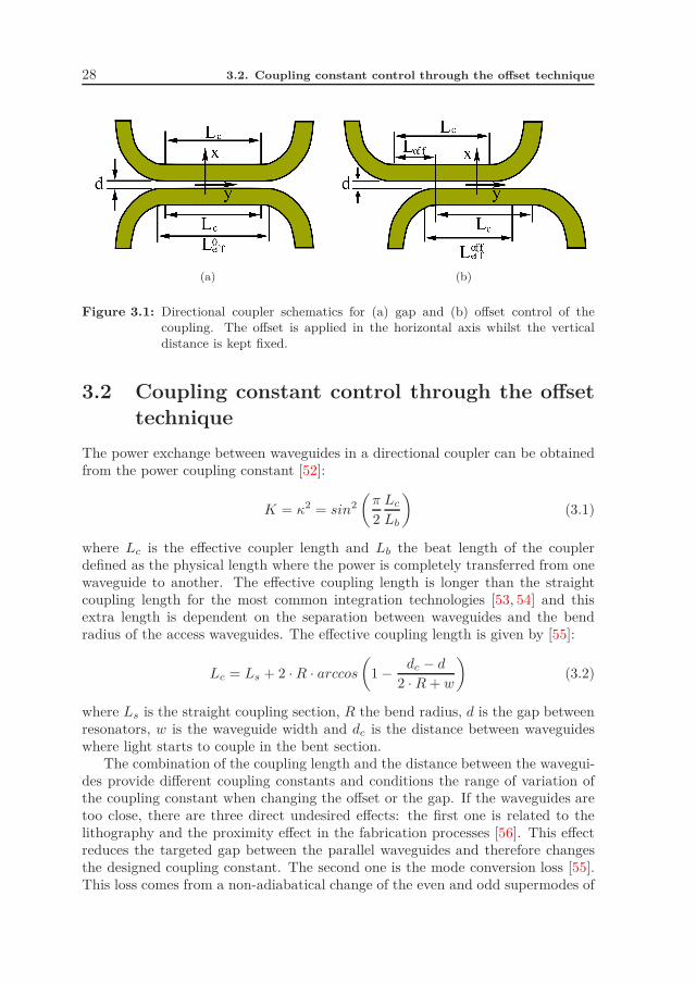
28 3.2. Coupling constant control through the offset technique
L0ef f
Lcx
yd
Lc
(a)
d
c
Loff
Loffef f
Lc
x
y
L
(b)
Figure 3.1: Directional coupler schematics for (a) gap and (b) offset control of thecoupling. The offset is applied in the horizontal axis whilst the verticaldistance is kept fixed.
3.2 Coupling constant control through the offset
technique
The power exchange between waveguides in a directional coupler can be obtainedfrom the power coupling constant [52]:
K = κ2 = sin2
(
π
2
LcLb
)
(3.1)
where Lc is the effective coupler length and Lb the beat length of the couplerdefined as the physical length where the power is completely transferred from onewaveguide to another. The effective coupling length is longer than the straightcoupling length for the most common integration technologies [53, 54] and thisextra length is dependent on the separation between waveguides and the bendradius of the access waveguides. The effective coupling length is given by [55]:
Lc = Ls + 2 ·R · arccos(
1 − dc − d
2 · R+ w
)
(3.2)
where Ls is the straight coupling section, R the bend radius, d is the gap betweenresonators, w is the waveguide width and dc is the distance between waveguideswhere light starts to couple in the bent section.
The combination of the coupling length and the distance between the wavegui-des provide different coupling constants and conditions the range of variation ofthe coupling constant when changing the offset or the gap. If the waveguides aretoo close, there are three direct undesired effects: the first one is related to thelithography and the proximity effect in the fabrication processes [56]. This effectreduces the targeted gap between the parallel waveguides and therefore changesthe designed coupling constant. The second one is the mode conversion loss [55].This loss comes from a non-adiabatical change of the even and odd supermodes of

3. Longitudinal offset technique for apodization of CROWs 29
0 0.5 1 1.5 2 2.5 3 3.5 40
0.2
0.4
0.6
0.8
1
Leff
/Lc
K
Leffoff
Leff0
(a)
0 0.5 1 1.5 2 2.5 3 3.5 40
0.2
0.4
0.6
0.8
1
Leff/Lb
K
Leff
0
Leff
off
(b)
Figure 3.2: Illustration of the coupling constant change as the effective coupling lengthchanges. In the first case (a) a reduction in the effective coupling lengthimplies an increase in the coupling constant. In the second example (b) areduction of the effective coupling length implies a decrease in the couplingvalue.
the device between the coupling section and the curves. When the air gap betweenthe waveguides decreases, the mode shape difference between sections increases,and hence the mode conversion loss increases. Therefore the loss parameter ofthe coupler introduced in equation 2.5 is no longer γ = 1. The last one is thecoupling-induced resonance frequency shifts (CIFS) [57]. Depending on the res-onators geometry and their coupling scheme, CIFS can strongly distort the filterresponse. The CIFS effect in CROWs appears as an asymmetry in the spectra. Incoupled resonator structures, the frequency shift is related to phase perturbationsin the couplers. Depending on the technology, the CIFS effect can be minimizedby employing the appropriate gaps in the coupler sections.
The proposed longitudinal offset technique allows for both increasing and de-creasing the value of K, starting from a nominal value. This is shown in Fig. 3.2-aand Fig. 3.2-b respectively. In both figures, L0
eff is the coupling effective length
without offset, as in Fig. 3.1-a, while Loffeff is the coupling effective length with
offset, as in Fig. 3.1-b. In Fig. 3.2-a, L0eff is such a way that the starting K value
is at a negative slope over coupler transfer function vs. effective length. Therefore,a reduction in the effective length, down to Loffeff , will imply an increase in the K
value. In Fig. 3.2-b, L0eff is such a way that the starting K value is at a positive
slope over coupler transfer function vs. effective length. Therefore, a reduction inthe effective length, down to Loffeff , will imply a decrease in the K value. Each ofthese two mentioned techniques can be applied for the apodization of SCISSORsas well as for CROWs, as already shown in the previous chapter.

30 3.3. Coupling constant sensitivity analysis
3.3 Coupling constant sensitivity analysis
The analysis shown is focused in the fabrication imperfections in Silicon-On-Insulator (SOI) technology using photolithographic processes, which is the tech-nology used in the fabricated devices presented in this thesis, as motivated inChapter 1. The resolution of the lithography equipments is in the order of fiveto ten nanometers but can be increased by post-processing the mask [58]. Animportant characteristic of the photolithographic processes is the exposure dose.In the fabrication process, this dose can be changed progressively from left to rightof the wafer covering a deviation from the nominal thickness of the features in themask [59]. In this section, a detailed analysis of the coupling in the directional cou-plers employed for the CROW structures will be shown. The coupling values havebeen numerically determined with the Beam Propagation Method (BPM) [60].All the simulations have been carried out in 3 dimensions with a spatial resolutionof 1x1x1 nm3. The simulated layer stack recreates SOI wafers manufactured bySOITEC employed in the ePIXfab fabrication platform [24], 220 nm height Siliconcore on top of 2 micrometers of SiO2. The coupler lengths shown in the nextsections have been chosen to show two different case studies: in the first case, thecoupler length is 53.3 µm and the distance between the waveguides is d = 150 nm,hence the starting K value is at a negative slope over coupler transfer function,and therefore a longitudinal offset implies an increase in the coupling constant; inthe second case a coupler length of 20 µm and waveguide separation of d = 100nm are used, being the starting K value at a positive slope over coupler transferfunction, and hence an offset implies a decrease in the coupling constant.
3.3.1 Gap apodized CROWs
For the CROW structures where the control of the coupling constant value isset by changing the lateral spacing between waveguides, the fabrication processresolution is a limitation [61]. Figs. 3.3-a and 3.3-b show the results of the 3DBPM simulations of a directional coupler with nominal length of 53.3 µm and 20µm respectively. The distance between centres (d0 in Figs. 3.3-a and 3.3-b) is keptconstant for each sweep of the waveguide width (from 480 to 520 nm) in order torecreate the variation of the exposure dose in the fabrication process. The verticalaxis represents the variation in the coupling constant as d0 increases. In both cases,an increase of d0 represents a decrease in the coupling constant. From Figs. 3.3-aand 3.3-b can be extracted that a small variation in d0 (below the fabricationresolution) implies a significant change in the coupling constant. On the otherhand, the horizontal axis reveals that for variations in the features sizes given byan over/down-exposure, the change in the coupling values is much less significantin the range studied. The latter effect can be explained as a compensation betweenthe change of the distance between waveguides, d (d = d0 − w), and the changein the confinement of the evanescent tails of the electric field related to a changein the waveguide width. Therefore, in this kind of couplers, to accurately set thedesired coupling constants a resolution of nanometers in the fabrication process is

3. Longitudinal offset technique for apodization of CROWs 31
480 485 490 495 500 505 510 515 5200.60
0.62
0.64
0.66
0.68
0.70
0.72
0.74
0.76
0.78
0.80
Waveguide width [nm]
0.1
0.2
0.3
0.4
0.5
0.6
0.7
0.8
0.9
d0 [
μm
]
0
(a)
480 485 490 495 500 505 510 515 5200.60
0.62
0.64
0.66
0.68
0.70
0.72
0.74
0.76
0.78
0.80
Waveguide width [nm]
0.1
0.2
0.3
0.4
0.5
0.6
0.7
0.8
0.9
d0 [
μm
]
1
(b)
Figure 3.3: Coupling constant (K) vs waveguide width and distance between wavegui-des centers (d0) for a nominal waveguide width w = 500 nm and a couplerlength of 53.3 µm (a) or 20 µm (b).
needed, which is technologically challenging nowadays.The resolution required for the fabrication of gap apodized CROWs can be
achieved by means of electron beam lithography (EBL). The resolution achievedby direct-writing techniques can be well below 10 nm [62]. Even though EBL canallow accurate dimensional control [63], it is slow, complex, expensive and, dueto the small writing area, it is unsuitable for mass production. The state-of-the-art photolithography equipments employed for photonics are using 193 nm Deep-Ultra-Violet (DUV) illumination [64]. The resolution that can be achieved withsuch a wavelength is in the order of 5 to 10 nm for isolated lines but undesiredeffects as Optical Proximity Effect [56] can affect the fabrication performance.When an isolated line comes in close proximity with another line (e.g., in anoptical coupler), the line widths of both lines reduce as a function of the distancebetween them. There are techniques to correct these effects but the correctionsrequired for gaps below 200 nm are much more important than for the gaps above200 nm. In both cases, the final resolution will be given by a combination ofthe lithography technique plus the etching process employed. The etching processtypically employed in SOI foundries is the inductively coupled plasma-reactive ionetching (ICP-RIE) [64].
3.3.2 Offset apodized CROWs
BPM analysis of the directional coupler with offsets is performed as well and theresults are shown in Figs. 3.4-a and 3.4-b. The vertical axis here represents thevariation of the coupling constant as the longitudinal offset increases/decreases.In this case, the variation of the coupling constant is controlled by changing thewaveguides position in steps of micrometers or of hundreds of nanometers, a morerelaxed condition than in the case of varying the gap. On the other hand, in the

32 3.4. Transfer Matrix analysis
0.25
0.30
0.35
0.40
0.45
0.50
0.55
0.60
0.65
0.70
0.75
480 485 490 495 500 505 510 515 5200
1
2
3
4
5
6
7
8
9
10
Waveguide width [nm]
Off
set
[μm
]
0.20
(a)
480 485 490 495 500 505 510 515 5200
2
4
6
8
10
12
14
16
18
20
Waveguide width [nm]
0.1
0.2
0.3
0.4
0.5
0.6
0.7
0.8
0.9
Off
set
[μm
]
0
1
(b)
Figure 3.4: Coupling constant (K) vs waveguide width and longitudinal offset betweenthe coupler waveguides for a nominal waveguide width w = 500 nm and acoupler length of 53.3 µm (a) or 20 µm (b).
horizontal axis the waveguides width change as the exposure doze varies is plotted.Figs. 3.4-a and 3.4-b show the calculated coupling constants for coupler lengthsof 53.3 µm and 20 µm respectively. This two coupler lengths have been chosen toillustrate the two cases previously exposed in Fig. 3.2: the longitudinal offset canimply an increase of the coupling constant as in Fig. 3.4-a or a decrease as shownin Fig. 3.4-b.
Looking carefully at the scales of the vertical axis in Fig. 3.3, in the gap controlof coupling, in order to obtain a change in the coupling constant of 0.5 a variationof tens of nanometers is required in the gap, whilst in the offset case (Fig. 3.4) for asimilar variation, an offset of several microns is needed. Therefore the sensitivityof the offset technique is significantly higher compared with the gap case, andhence the control of the coupling becomes an easier task. The robustness of thistechnique will be demonstrated in the next section through several examples ofCROWs for which spectral response has been calculated by the Transfer MatrixMethod.
3.4 Transfer Matrix analysis
The frequency response of several CROWs has been calculated through the TMMformalism derived in Section 2.3.2 in order to compare the performance of bothmethods presented for the control of coupling constants in CROWs. Two CROWswith 3 and 5 racetrack resonators for each coupling scheme have been studied:uniform (non-apodized), gap apodized and offset apodized. The value of the cou-pling constants has been extracted from the BPM simulations presented in theprevious section. Fig. 3.5 shows the ideal spectrum calculated with MatlabTMforthe 3 and 5 racetracks CROWs for the uniform and apodized cases. The spectra

3. Longitudinal offset technique for apodization of CROWs 33
UniformApodized
-0.5 -0.4 -0.3 -0.2 -0.1 0 0.1 0.2 0.3 0.4 0.5
-45
-40
-35
-30
-25
-20
-15
-10
-5
0
δ /2π
Tra
nsm
issi
on [
dB
]
(a)
UniformApodized
-0.5 -0.4 -0.3 -0.2 -0.1 0 0.1 0.2 0.3 0.4 0.5
-45
-40
-35
-30
-25
-20
-15
-10
-5
0
δ /2π
Tra
nsm
issi
on [
dB
]
(b)
Figure 3.5: Transmission for 3 (a) and 5 (b) racetracks CROW. The uniform response(K=0.2 in all couplers) is depicted in continuous line and the apodizedresponse (K values from the table) is depicted with the dashed line.
shown are limited to a single FSR expressed in normalized units of δ/2π, being δas introduced in equation 2.17:
δ = βLc =2π
λ· c · ng · Lc (3.3)
with Lc the optical path length of a single cavity, c the speed of light in vacuumand ng the group index of the waveguides defined as:
ng = neff − λ · ∂neff∂λ
(3.4)
where neff is the modal effective index.Tables 3.1-(a) and 3.1-(b) summarize the coupling constants and the gaps or
offsets required by design in order to obtain the ideal (lossless) apodized responsecalculated through the Transfer Matrix Method and depicted in Fig. 3.5. Theoffsets and gaps presented have been extracted also from the BPM simulations forboth coupler lengths of 53.3 µm and 20 µm. All the spectra shown, are underthe assumption that fabrication is done with infinite resolution, so the gaps andoffsets required for the apodization can be accurately achieved. In practice this islimited by the fabrication process, leading to restrictions in the designs.

34
3.4
.T
ra
nsfe
rM
atrix
an
aly
sis
Table 3.1: 3 and 5 racetrack gap and offset apodized CROW
(a) 3 racetrack CROW
Hamming window apodization[Lc=53.3 µm] [Lc=20 µm] [Lc=53.3 µm] [Lc=20µm]
Coupler # Kn Gap [nm] Gap [nm] Offset [µm] Offset [µm]1 0.70616 124.90 147.90 9.858 7.1222 0.30449 183.90 210.10 1.464 12.4803 0.30449 183.90 210.10 1.464 12.4804 0.70616 124.90 147.90 9.858 7.122
(b) 5 racetrack CROW
Hamming window apodization[Lc=53.3 µm] [Lc=20 µm] [Lc=53.3 µm] [Lc=20µm]
Coupler # Kn Gap [nm] Gap [nm] Offset [µm] Offset [µm]1 0.74065 119.80 141.00 10.650 6.6122 0.52663 151.30 173.10 6.080 9.5403 0.24870 192.10 216.70 0.193 13.2904 0.24870 192.10 216.70 0.193 13.2905 0.52663 151.30 173.10 6.080 9.5406 0.74065 119.80 141.00 10.650 6.612

3. Longitudinal offset technique for apodization of CROWs 35
480nm490nm500nm510nm520nm
-0.5 -0.4 -0.3 -0.2 -0.1 0 0.1 0.2 0.3 0.4 0.5-30
-25
-20
-15
-10
-5
0
δ/2π
Tra
nm
issi
on [
dB
]
Lc=53.3μm
(a)
480nm490nm500nm510nm520nm
Lc=53.3μm
-0.5 -0.4 -0.3 -0.2 -0.1 0 0.1 0.2 0.3 0.4 0.5-30
-25
-20
-15
-10
-5
0
δ/2π
Tra
nm
issi
on [
dB
]
(b)
480nm490nm500nm510nm520nm
Lc=53.3μm
-0.5 -0.4 -0.3 -0.2 -0.1 0 0.1 0.2 0.3 0.4 0.5
-45
-40
-35
-30
-25
-20
-15
-10
-5
0
δ /2π
Tr
mis
sio
n [
dB
]
(c)
480nm490nm500nm510nm520nm
Lc=53.3μm
-0.5 -0.4 -0.3 -0.2 -0.1 0 0.1 0.2 0.3 0.4 0.5
-45
-40
-35
-30
-25
-20
-15
-10
-5
0
δ /2π
Tra
nsm
issi
on
[d
B]
(d)
Figure 3.6: Transmission spectrum for 3 (a)(b) and 5 (c)(d) racetrack gap (a)(c) andoffset (b)(d) apodized CROWs vs several waveguide widths simulating thevariation in the exposure dose. The nominal width employed in the designsis w = 500 nm and the coupler length is 53.3 µm.
Fig. 3.6 shows the simulation of two gap apodized CROW and two offset apo-dized CROW of 3 and 5 cavities respectively with a straight section of 53.3 µm inthe couplers. The coupling constants have been extracted from the BPM simula-tions shown in Figs. 3.3 and 3.4. The coloured lines represent a variation in thewaveguide width whilst keeping constant the nominal distance between centres.These variations in the waveguides width represent the effect of the variation in theexposure doze that can be applied in the photolithographic process. This variationwill be explained with more detail in the next chapter. Comparing the 3 racetrackresonators CROW for the gap (Fig. 3.6-a) and for the offset (Fig. 3.6-b) apodi-zation cases, the ripples in the pass-band and the bandwidth of the filter presentlower variations in the offset case than in the gap case. The results are similar forthe 5 racetrack resonators case (Fig. 3.6-c vs Fig. 3.6-d). In the gap apodizationcase, the 3 and 5 racetrack resonators CROW response starts to deviate from thetarget showing an increased spectral width and a reduced out-of-band rejection.

36 3.4. Transfer Matrix analysis
-0.5 -0.4 -0.3 -0.2 -0.1 0 0.1 0.2 0.3 0.4 0.5-30
-25
-20
-15
-10
-5
0
δ��π
Tra
nm
issi
on [
dB
]
480nm490nm500nm510nm520nm
Lc=20μm
(a)
480nm490nm500nm510nm520nm
-0.5 -0.4 -0.3 -0.2 -0.1 0 0.1 0.2 0.3 0.4 0.5-30
-25
-20
-15
-10
-5
0
δ/2π
Tra
nm
issi
on [
dB
]
Lc=20μm
(b)
-0.5 -0.4 -0.3 -0.2 -0.1 0 0.1 0.2 0.3 0.4 0.5-50
-45
-40
-35
-30
-25
-20
-15
-10
-5
0
δ /2π
Transmissio
n [
dB
]
480nm490nm500nm510nm520nm
Lc=20μm
(c)
480nm490nm500nm510nm520nm
Lc=20μm
-0.5 -0.4 -0.3 -0.2 -0.1 0 0.1 0.2 0.3 0.4 0.5-50
-45
-40
-35
-30
-25
-20
-15
-10
-5
0
δ /2π
Tra
nsm
issi
on
[d
B]
(d)
Figure 3.7: Transmission spectrum for 3 (a)(b) and 5 (c)(d) racetrack gap (a)(c) andoffset(b)(d) apodized CROWs vs several waveguide widths simulating thevariation in the exposure dose. The nominal width employed in the designsis w = 500 nm and the coupler length is 20 µm.
Fig. 3.7 shows the same comparison as in the previous example of Fig. 3.6 butin this case the straight coupling section has been reduced to 20 microns. In thisexample, the comparison of Fig. 3.7-a vs Fig. 3.7-b and Fig. 3.7-c vs Fig. 3.7-d appears to be better for the gap case than for the offset case. In any case thevariations presented in the spectra are small enough to fit the design requirements.Despite the results can be interpreted as if both methods present similar robustnessagainst fabrication imperfections this is not true. In most cases, the requiredgap changes are below the fabrication resolution or close to its limit. On theother hand, employing the longitudinal offset apodization technique, the offsetsrequired for setting the coupling constants are well above the resolution limit ofthe fabrication processes. This will lead to distorted or out of target responsesin the fabricated devices for the gap case and not for the offset case. In the nextchapter, the experimental demonstration of this longitudinal offset technique forthe apodization of CROW devices is shown.

3. Longitudinal offset technique for apodization of CROWs 37
3.5 Conclusions
A novel technique for controlling the coupling between racetracks in SCISSORor CROW structures has been presented. This technique allows a better controlof the coupling typically limited by the fabrication resolution. The sensitivity isincreased critically by using the longitudinal offset technique despite the increasein the footprint of the final devices. It has been demonstrated through simulation,how the apodization of Coupled Resonator Optical Waveguides through the lon-gitudinal offset technique is as effective as with conventional techniques, reducingthe accuracy required for fabrication. As expected, the ripples within the passbandtransmission and group delay are reduced through apodization.
The main benefits of the longitudinal offset apodization technique are:
• Allows for an accurate setting of the coupling constant in the unit cells ofCROW and SCISSOR devices
• Reduces the tight fabrication requirements for coupled resonator devices
• Allows for the use of mass production techniques in the fabrication of coupledresonator devices
• Can be employed in CROWs, SCISSORs or any device containing directionalcouplers
Via the Universitat Politecnica de Valencia (UPV) Technology Transfer Office, thelongitudinal offset technique has been patented at a national level (Patent NumberP200901145 - 4/23/09). The patented technology has been licensed to the UPVSpin-Off company VLC Photonics S.L. for its exploitation.

38 3.5. Conclusions

Chapter 4
Design and fabrication of Coupled
Resonators in Silicon On Insulator
4.1 Introduction
In this chapter the design, fabrication and characterization of CROWs in SiliconOn Insulator (SOI) technology will be studied in detail. The design of CROWdevices through its conforming sub-structures analysis and characterization willbe reported, from simple waveguides to the basic unit cell of CROWS: the ringresonator. The experimental results obtained will be compared to the theoreticalpredictions calculated with the models developed in the previous chapters. TheCROW devices described in this chapter implement the longitudinal offset tech-nique for setting the coupling constants that has been introduced and developedin the previous chapter.
4.2 Fabrication details
Silicon photonics is one of the most promising technologies for the future photonicintegrated circuits [23]. The Silicon Photonics technology platform offers passivelight manipulation at a very small footprint, allowed by the relative high contrastindex of silicon. Such small chip size, its cheaper base material and its CMOSfabrication compatibility also results in a lower chip price. However, no light am-plification is possible at the time other than hybrid integration [65], meaning thatintegration with other technologies will be required for some active functionalities.In the following subsections, the fabrication technology will be introduced as wellas the access scheme employed for the prototyping in the selected technology.

40 4.2. Fabrication details
1 2 3 4 5 6 7 8 9 10 11
1
2
3
4
5
6
7
8
9
10
11
12
COLUMN
ROW
1
3 4
5 6
7 8
Figure 4.1: Schematic of the wafer partitioning and exposure. The wafer is divided inrows and columns to conform the dies containing the users designs. Thenotch in the bottom of the wafer indicates its crystallographic orientationand it is used as a reference for positioning the bottom side of the wafer.The inset on the top right part shows how a single die is divided into sub-dies that can be filled with designs from different users. The picture fromthe bottom right inset shows one of the fabricated wafers.
Multi-Project-Wafer runs
Several sets of CROWs with and without apodization have been fabricated in Sil-icon On Insulator technology during the realization of this thesis. The fabricationruns have been carried out in several Multi Project Wafer (MPW) runs within theePIXfab platform [24]. In these MPW runs, the users can share fabrication costsby means of sharing process steps and wafer space. The wafer is divided in dieslimited in size by the step and repeat lithography equipment. The maximum diesize is approximately 25 x 25 mm2 because of commonly available CMOS machin-ery employed for fabrication, in the case of ePIXfab, the equipment is the ASMLPAS5500/1100 step-and-scan system. Every die is sub-divided in smaller sub-diesthat are filled with the designs of individual users and every user receives a fixednumber of dies. The dies can be diced individually for each user to receive itsown design or one can choose to receive a full die. The intellectual property isprotected by employing a laser process to remove other customers’ integrated cir-cuit designs from the MPW while leaving specified designs intact. Fig. 4.1 showsthe partitioning of the wafer in dies and the inset at the right shows how eachdie is divided into smaller sub-dies allocatable to different users. The wafer ishence divided in columns/rows. Although the designs within a die may well bedifferent (designs come from distinct users) the fabrication process is the same.Nonetheless, the exposure doze can be varied per column. The exposure dose isthe intensity of DUV light per area unit that is applied to the photoresist on top of

4. Design and fabrication of Coupled Resonators in Silicon On Insulator 41
the wafer. The variation in the exposure dose introduces variations in the featuressizes. A low exposure dose makes the waveguides wider and the gaps narrower anda high exposure dose makes the waveguides narrower and the gaps wider. Typ-ically this exposure dose is varied from left to right incrementally. The left andright parts can be distinguished with the help of the notch in the wafer indicatingthe bottom part as shown in Fig. 4.1. During the fabrication process, at somespecific steps, measurements of critical dimensions in the designs are made withscanning electron microscopy. For instance, after every etching level, the width ofthe waveguides is controlled. The users can define a set of critical dimensions intheir designs that will be monitored and reported after the fabrication. A criticaldimension is a measurement of a feature in the design (i.e. a waveguide width).These values are used as reference for checking the fabrication process.
Fabrication Technology
The devices reported in this thesis were fabricated in the CMOS line of imec (theInter University Microelectronics Center), Leuven, Belgium. The access to thefabrication runs was possible through the ePIXfab [24] service. ePIXfab organizesMPW shuttles in silicon photonics technologies. This allows researchers/engineersto prototype silicon photonic ICs at affordable cost. For the users, this fablessscheme allows them to focus on device and application ideas, design and character-ization. The technologies that ePIXfab offers are high-end wafer scale CMOS-typefabrication technologies. Setting up and maintaining a fab with such a complextechnology is only possible for a few companies and research institutes in the world.All ePIXfab fabrication is done on production-type tools. The fabrication is car-ried out on 200 mm SOI wafers, manufactured by SOITEC, processed with 193 nmdeep Ultra Violet (DUV) lithography and dry etching. Details of the fabricationprocesses employed can be found in [59, 64].
4.3 Building blocks design
In these fabrication runs several building blocks (BB) were designed and fabricated,as waveguides, directional couplers and racetrack resonators amongst others, toconform the CROW devices under study in this work. For the design of these build-ing blocks, the most relevant parameters were scanned through multi-parametric(computer-aided) analysis. For instance the geometry of the waveguides whencomputing the propagating modes, the wavelength dependency of the refractiveindices of the materials and also the wavelength dependency of the coupling con-stant in the parallel waveguides couplers.
The waveguides
The fundamental BB for all the structures is the waveguide. Optical waveguidesin SOI technology should provide low propagation losses and small bending ra-

42 4.3. Building blocks design
Si
SiO2
Si
Air / SiO2
220nm
(a)
Si
SiO2
Si
Air / SiO2
70nm
(b)
Figure 4.2: Deeply (a) and Shallowly (b) etched waveguide cross-sections in a typicalSOI layerstack. The top cladding can be different depending on the appli-cation. The typical etching levels for the two configurations shown are 220nm and 70 nm.
dius whilst ensuring single mode propagation and polarization independence. Thetransverse electric (TE) and transverse magnetic (TM) modes have very differenteffective index and propagation loss. Polarization independency is very hard toachieve, although it is possible to change this by altering the core form factor [66].The waveguides height is defined in the wafer fabrication process. The guidingSilicon layer thickness for photonic applications is in the range between 220 nmto 5 microns. Depending on this thickness, and in combination with the widthand the Buried Oxide (BOX) substrate thickness, the waveguide will support adifferent amount of propagating modes. The standard Silicon height adopted bymost of the SOI foundries running MPW runs is 220 nm on top of 2 microns BOX.This thickness provides tight confinement and moderate propagation losses, andtogether with the appropriate etching levels also allows for ultra small bending ra-dius. This combination of properties makes possible the creation of miniaturizedphotonic circuits. From the designer point of view, there are only two free designparameters regarding the waveguides: the width and the etching. The etchinglevels are also predefined by the foundry and there are typically two etching levelsto conform the deep (DE) and shallowly (SH) etched waveguides. In the case ofimec, the etching levels are 220 nm and 70 nm for the DE and the SH waveguidesrespectively. Fig. 4.2 shows the cross-section of the deep and shallowly etchedwaveguides in SOI. The difference between SH and DE waveguides is the opticalconfinement. Confinement has impact in both the propagation loss for straightwaveguides, and the minimum bend radius for bent waveguides. Propagation lossis mainly due to surface roughness, which is felt by the mode propagating withinthe waveguide. DE waveguides sidewalls are hence more prone to roughness dueto etching all down the film. Therefore, the propagation loss for DE waveguidesis larger than for SH waveguides. Typical values for DE waveguides are in therange from 2 to 3 dB/cm [67] and for the SH from 0.5 to 1.5 dB/cm [68]. One

4. Design and fabrication of Coupled Resonators in Silicon On Insulator 43
350 400 450 500 550 600
1.6
1.8
2.0
2.2
2.4
2.6
Waveguide width [nm]
nef
f TE
0
Si
SiO2
200nm
(a)
350 400 450 500 550 600
1000
1200
1400
1600
1800
2000
Waveguide width [nm]
Wav
elen
gth
[n
m]
Modes
TE 0 cu
toff
TE1 cutoff
TM1 cutoff
TM0 cutoff
No
(b)
Figure 4.3: (a) T E0 effective modal index (neff ) as a function of the waveguide widthat a wavelength of λ = 1.55µm for a deep-etch waveguide with air cladding.The right inset shows the T E0 mode profile for a width of 450 nm. The leftinset shows a Scanning Electron Microscope image of the cross-section of a450 nm width SOI waveguide. (b) Cut-off wavelength of a DE waveguidefor the two lowest order TE and TM modes as a function of the waveguidewidth. The pink area shows single-mode support for TE and the blue areafor TM polarization.
of the techniques employed for loss reduction in air or Silica cladding waveguidesis a thermal oxidization step after the etching. With this technique, the surfaceroughness is reduced at a cost of loosing some nanometers of the Silicon guidinglayer that are transformed in Silicon Dioxide. The minimum bend radius is de-pendent on the confinement. In the SH waveguides the modes are less confined inthe core than in the DE waveguides due to the reduced index contrast, this allowsto employ smaller bend radius in the DE waveguides. In the case of SOI, bendradius down to 1.5 microns have been demonstrated [69]. The cladding in bothconfigurations can be either Silicon Oxide or just air. The main difference arisesfrom the index contrast and therefore is reflected in the confinement. Wavegui-des that have a Silicon Oxide cladding present a slightly reduced index contrastthan unclad waveguides but are less exposed to external agents like temperature,humidity, etc. For biosensing applications, waveguides without cladding (i.e. air)are most suitable [70].
In the devices presented in this work, the waveguides have no cladding (air) andare deeply etched. In order to choose the appropriate width, a commercial modesolver based on Finite Differences (FieldDesignerTM) from Phoenix Software [28]has been employed. The effective index of the first transverse-electric (TE) modefor a wavelength of 1.55 µm has been calculated for waveguide widths varyingfrom 350 to 600 nm as shown in Fig. 4.3-(a). The insets of the figure show the TEmode profile for a waveguide width of 450 nm and a SEM image of a fabricatedwaveguide. For the devices presented in this thesis, widths of 500 nm and 450 nm

44 4.3. Building blocks design
1.5 1.52 1.54 1.56 1.58 1.62.2
2.225
2.25
2.275
2.3
2.325
2.35
Mo
dal
eff
ecti
ve
ind
ex (
TE
0)
Wavelength [nm]
(a)
1.5 1.52 1.54 1.56 1.58 1.60.65
0.7
0.75
0.8
0.85
0.9
0.95
1
Wavelength [nm]
Co
up
lin
g C
on
stan
t 'K
'
(b)
Figure 4.4: Modal effective index (a) numerically calculated for a waveguide geometryof 220 x 450 nm2 and power coupling constant (b) numerically calculated fora directional coupler with the same waveguide geometry and a separationof 200 nm between waveguides. Both graphs have been calculated for SOItechnology employing PhoeniX software .
have been employed in two different fabrication runs. As shown in Fig. 4.3-(b),these widths allow for TE monomode propagation at the working wavelength of1550 nm. The cut-off wavelengths shown in Fig. 4.3-(b) have been calculated withthe MIT software MPB [71] following the methodology described in [72]. Fig. 4.4-a shows the calculated effective index of the first TE mode propagating in thewaveguide and its wavelength dependency for a DE waveguide of 220 x 450 nm.
The couplers
The second BB under test has been the directional coupler (DC). The DC is wellknown [35] and it consists of two waveguides running in parallel. When the lateraldistance between them is such that the tails of the individual modes overlap, thewaveguides are coupled. This is also known as evanescent field coupling. Thepower is exchanged periodically between the waveguides. At a distance called thebeat length the power is transferred completely from one waveguide to anotheras explained in section 3.2. Figure 4.5-a shows the SEM images of two of thefabricated and measured devices. The first one is a symmetric directional couplerand the second one is a directional coupler with a longitudinal offset. The couplersphysical parameters are: a cross-section of 220 x 450 nm, a straight coupling sectionof 15µm, 5µm bend radius and a gap between waveguides of 200 nm. The couplershown in the bottom of Fig.4.5-a also includes a longitudinal offset of 3µm.
Figure 4.5-b shows the measured power coupling constant (K) for the twodirectional couplers depicted in Fig. 4.5-a. The measurements have been carriedout in the following way: first a reference straight waveguide is measured fornormalization purposes. Later the spectra from the two outputs is captured when

4. Design and fabrication of Coupled Resonators in Silicon On Insulator 45
Ls
Ls
Ls
Offset
(a)
1535 1540 1545 1550 1555 1560 1565 15700
0.1
0.2
0.3
0.4
0.5
0.6
0.7
0.8
0.9
1
Wavelength [nm]
Coupli
ng c
onst
ant
'K'
Offset 0µmOffset 3µm
(b)
Figure 4.5: (a) SEM images of fabricated symmetric directional couplers and witha longitudinal offset. (b) Measured coupling constant for both couplers.The blue line refers to the symmetric directional coupler and the red linerepresents the measured data for the directional coupler with a longitudinaloffset of 3 µm
injecting light from one of the input ports. The power coupling constant K is thencalculated as the power measured in the cross port divided by the total power (inthis case calculated as the sum of the power detected at the two output ports). Themeasurements obtained from both output ports are normalized with the referencemeasurement to eliminate the effect of the grating couplers. The graph shows thewavelength dependency of the coupling constant for the chosen coupler geometryfollowing equation 3.1. The blue line corresponds to the uniform coupler and thered line corresponds to the coupler with a longitudinal offset. As presented insection 3.2, for a given coupler length, the introduction of a longitudinal offset caneither increase or decrease the coupling constant in a directional coupler. In thiscase by applying an offset of 3 µm and therefore reducing the effective couplinglength, the coupling constant is decreased as can be derived from the measurementsshown in Fig. 4.5-b.
Racetrack resonators
The basic unit cell of the CROW structures designed in this work are the racetrackresonators. CROW structures are typically conformed either by ring resonators orracetrack resonators. In this work, racetrack resonators have been employed giventhat these structures allow to better implement the longitudinal offset techniquefor setting the coupling constants in the CROW device. Rings can also be usedbut control would be uncertain. Fig. 4.6-a shows a SEM picture of a dual-bus
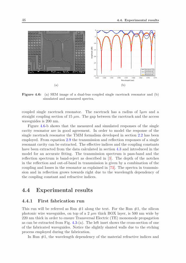
46 4.4. Experimental results
(a)
1535 1540 1545 1550 1555 1560 1565 1570 1575-35
-30
-25
-20
-15
-10
-5
0
Wavelength [nm]
Am
pli
tude
[dB
]
Simulated TXSimulated RFMeasured TXMeasured RF
(b)
Figure 4.6: (a) SEM image of a dual-bus coupled single racetrack resonator and (b)simulated and measured spectra.
coupled single racetrack resonator. The racetrack has a radius of 5µm and astraight coupling section of 15 µm. The gap between the racetrack and the accesswaveguides is 200 nm.
Figure 4.6-b shows that the measured and simulated responses of the singlecavity resonator are in good agreement. In order to model the response of thesingle racetrack resonator the TMM formalism developed in section 2.2 has beenemployed. From equation 2.9 the transmission and reflection responses of a singleresonant cavity can be extracted. The effective indices and the coupling constantshave been extracted from the data calculated in section 4.3 and introduced in themodel for an accurate fitting. The transmission spectrum is pass-band and thereflection spectrum is band-reject as described in [3]. The depth of the notchesin the reflection and out-of-band in transmission is given by a combination of thecoupling and losses in the resonator as explained in [73]. The spectra in transmis-sion and in reflection grows towards right due to the wavelength dependency ofthe coupling constant and refractive indices.
4.4 Experimental results
4.4.1 First fabrication run
This run will be referred as Run #1 along the text. For the Run #1, the siliconphotonic wire waveguides, on top of a 2 µm thick BOX layer, is 500 nm wide by220 nm thick in order to ensure Transversal Electric (TE) monomode propagationas can be extracted from Fig. 4.3-(a). The left inset shows the cross-section of oneof the fabricated waveguides. Notice the slightly slanted walls due to the etchingprocess employed during the fabrication.
In Run #1, the wavelength dependency of the material refractive indices and

4. Design and fabrication of Coupled Resonators in Silicon On Insulator 47
R
κ1 κ2 κ3 κ4
Ls
(a)
κ1κ2 κ3
κ4
(b)
Figure 4.7: SEM images of a three racetrack uniform CROW (a) and three racetrackapodized CROW (b)
coupling constants was not taken into account. When neglecting the wavelengthdependency of n and K the results are only valid in a small range of wavelengths.In this case the fitting of the measurements and simulations are accurate in a sin-gle FSR. In SOI waveguides, the group index ng exceeds the refractive index ofbulk silicon, clearly indicating that in case of photonic wires with strong opticalconfinement the propagation constant of the waveguide is dominated by the wa-veguides’ geometry and not by material properties [72]. Regarding the couplingconstant, the wavelength dependency affects to the individual resonances withineach resonator in the CROW device. That is directly translated to a differentresponse for each FSR. Figures 4.7-(a) and 4.7-(b) show Scanning Electron Mi-croscope (SEM) images of the uniform and apodized CROW devices, respectively.The racetracks have a bend radius R = 5 µm and a straight section Ls = 53.3 µmin both devices. The measured linear propagation loss in such photonic wires is3 ± 1 dB/cm. The group index around 1.55 µm wavelength is ng ≃ 4.25. It hasbeen derived from the measured Free Spectral Range (FSR) of the CROW devices.The gaps between cavities in the uniform and apodized CROWs were set to 150nm. The spectral measurements presented in this section belong to the selecteddevices whose gaps were closest to the design gap. The devices were selected byperforming SEM and Atomic Forces Microscope (AFM) measurements on severaldies. In the fabrication process at imec, the guaranteed minimum gap was 120 nmand that is why 150 nm was chosen, to be on the safe side. For the uniform CROW,all the racetracks have the same coupling length and therefore the same couplingconstant that is K1 = K2 = K3 = K4 = 0.48. The couplings in the apodizedCROW have been set symmetrically: the longitudinal offset applied to the firstand last racetrack is the same and the resulting coupling constants have a value ofK1 = K4 = 0.86 and a different offset has been applied to the central racetrack,and as a result K2 = K3 = 0.54 as proposed in the previous chapter. Translating

48 4.4. Experimental results
Netw
ork
Analy
zerDUT
TL EDFA PDMZM
Pol. Control Pol. Control
RF out
RF in
Figure 4.8: Group delay characterization setup. Continuous lines represent optical sig-nals and dashed lines electrical signals.
the coupling values to physical parameters it is found that for a straight couplingsection of 53.3 µm, the actual coupling length is even longer and is given by Eq.(3.2). Apodization requires K1 = K4 = 0.86 and K2 = K3 = 0.54 as outlined be-low. This translates to a longitudinal offset of 10.56 µm and 2.42 µm respectively.Conversely the same apodization through a change of the coupler gap would re-quire gaps of 153 nm and 170 nm, for fixed Lc. Comparing the required changeswith both techniques it is clear that the longitudinal offset technique requires lessprecision and it is less sensitive when setting the coupling constants.
Power and Group Delay Measurements
The power and group delay transfer function were measured for the devices inFig.4.7 employing the setup shown in Fig.4.8 and the results are presented inFig.4.9. A tunable laser (ANDO AQ4321D, λ = 1520 − 1620 nm) was externallymodulated with a 100 MHz signal [74]. At the output of the modulator, the lightwas amplified with an Erbium Doped Fiber Amplifier (EDFA). The polarizationwas controlled both at the input of the modulator and at the input of the chip.The signal must be re-polarized because grating couplers [75] are used for in/outcoupling light into the device under test (DUT) and have been optimized for TEpropagation. At the output of the chip, the signal was then photodetected. Centralin this setup is the Microwave Networks Analyzer (Agilent, E8364A), which drivesthe modulator and receives the signals from the photodetector. It measures theamplitude and phase of the signal. The group delay is expressed in terms of thephase as follows [74]:
τg(λ) =φd(λ) + φ0
ωm(4.1)
where φd(λ) is the measured phase of the signal, φ0 is a constant phase term intro-duced by the setup in the absence of resonant structures and ωm is the modulationangular frequency. The term φ0 has been obtained by averaging several measuresdone on straight waveguides employing the same setup.
Fig.4.9 shows the measured amplitude and group delay (red lines) of the devicescompared with the theoretical responses (blue lines) calculated with the TMM de-scribed in chapter 2, where losses and the coupler length were taken into account.

4. Design and fabrication of Coupled Resonators in Silicon On Insulator 49
1550 1550.5 1551 1551.5 1552 1552.5 1553 1553.5 1554-25
-20
-15
-10
-5
0
0
2
4
6
8
10
12
14
16
Gro
up D
elay [p
s]
Tra
nsm
issi
on [
dB
]
Wavelength [nm]
18
(a)
1550 1550.5 1551 1551.5 1552 1552.5 1553 1553.5 1554-25
-20
-15
-10
-5
0
0
1
2
3
4
5
6
�
Gro
up D
elay [p
s]
Tra
nsm
issi
on [
dB
]
Wavelength [nm]
(b)
Figure 4.9: Power transmission and group delay responses of a 3 racetrack resonatoruniform CROW (a) and offset apodized (b). Blue lines (continuous forthe amplitude and dashed for the group delay) represent the theoreticalresponses and red lines represent the measured responses.
In the case of the uniform CROW, Fig. 4.9-(a), the measured transmission pass-band exhibit big ripples that have natural correspondence in the group delay.These ripples are due to the fact that all the coupling constants are equal [76].This was fully described by the theory in Chapter 2 and shown in Fig. 2.13 inthere. A mean delay of 5 ps has been measured with ripples of ±3 ps in a 3 dBbandwidth of 1.6 nm, as predicted by the transfer matrix calculations. For theoffset apodized CROW, Fig.4.9-(b), a flat response in transmission, due to theapodization of the structure, has been measured and a delay in the passband ofabout 4 ps with reduced ripples of ±0.5 ps in a 3 dB bandwidth of 1.4 nm.
4.4.2 Second fabrication run
In this fabrication run our designs contain, amongst other test structures, a setof CROWS with 3, 5, 7, 11, 21 and 31 racetrack resonators with and withoutapodization. This run will be referred as Run #2. Fig. 4.10 shows the SEM imagesof CROWs with 11 racetrack resonators. The images correspond to uniform andlongitudinal offset apodized CROW devices. The standard waveguide cross-sectionchosen was 450 x 220 nm2 and the minimum bend radius 5 µm. In the case ofthe racetracks, the gap between cavities has been set to 200 nm and the radiusfixed to 5 µm. The straight coupling section of the resonators chosen was 15 µm.The election of the straight coupling length was made to demonstrate the secondcase change in the coupling constant presented in Section 3.2 and illustrated inFig. 3.2-(b). In this case a decrease in the effective coupling length will result ina reduction of the coupling constant.
In Run #2, dose sweep was applied during the lithography step, in order tovary the feature size from the left side to the right side of the wafer (Fig. 4.1)

50 4.4. Experimental results
(a) (b)
Figure 4.10: SEM images of a 11 racetrack resonator uniform CROW (a) and apodizedwith the longitudinal offset technique (b).
as described in Section 4.2. As mentioned previously, during the fabrication, adose sweep has been applied in the lithography step and therefore the featureswill change from one side to the other of the wafer. Fig. 4.11 shows the effect ofthis variation in the dose. Figs. 4.11-a and 4.11-b show Field-Emission ScanningElectron Microscope (FESEM) images from the couplers of a test single racetrackresonator from a die within the first column. Figs. 4.11-c and 4.11-d show FESEMimages from the couplers of a test single racetrack resonator from a die within thelast column.
In the Run #1 was demonstrated how through the apodization, in the caseof CROWs of the direct coupling coefficients, the ripples in the passband of theCROW devices are reduced, but this happens at the cost of an increase in thefilter bandwidth as explained in Chapter 2.
In Run #2, the wavelength dependency of the neff and K haven’t been ne-glected. At long wavelengths the group index experiences a linear increase andthe coupling constant starts to decrease as was shown in section 4.3. When thiswavelength dependency is considered, the resonances of the CROW devices startto overlap due to an increase in the filter passband and a change in the FSR. Thisincrease in the passband is due to the change in the coupling constant. A slightchange in the filter periodicity can be observed as well and is mainly due to thegroup index change. When the response of the filter starts to overlap, the out ofband rejection starts to decrease. The cross coupling coefficients of the CROWdevices have been apodized in this run to increase the out-of-band rejection andhave more selective filters at a cost of course of reducing the filter bandwidth. Anapodization window that allows to increase the roll-off of the filters while keepingthe passband ripples at an acceptable level has been applied. Figure 4.12 shows thesimulated and measured group index of the fabricated CROWs. The group indexhas been derived from the FSR of the CROWs as in the previous sections but inthis case for three different wavelengths. The measurements show small deviationsfrom the simulation. These deviations arise from the fact that the measured FSR

4. Design and fabrication of Coupled Resonators in Silicon On Insulator 51
(a) (b)
(c) (d)
Figure 4.11: FESEM images of two directional couplers from a die within the middlecolumn of the wafer (a-b) and a die coming from the last column of thewafer (c-d). Both dies have been overexposed and therefore the waveguidewidths are out of target (450 nm). The variation on the exposure doze isreflected in the change of waveguide and gap widths.
employed to derive the group index may contain errors as well, given the difficultyof accurately determine the FSR because of the non-uniform shape of the spectralresponses. As expected, the group index ng is higher than in the fabrication Run#1 due to the reduced core size of the waveguides.
Figures 4.13 to 4.18 show the normalized TE simulated and measured spec-tra for the uniform and apodized CROW structures with 3, 5, 7, 11, 21 and 31racetracks. Sub-figures (a) and (c) show the transmission responses whilst in (c)and (d) the reflection responses are shown. The fitting between simulation andmeasurement is excellent for all the CROW devices, either uniform or apodized.
There exist two important differences between the theoretical and experimentalresults. First is the asymmetry of the spectrum response produced by the CIFS.The CIFS effect, introduced in Chapter 3, was accounted for when designing theCROW devices by introducing a gap between cavities big enough to minimize thisundesired effect. Even though, for some of the devices this effect is still present as

52 4.4. Experimental results
1525 1530 1535 1540 1545 1550 1555 1560 1565 1570 15754.50
4.51
4.52
4.53
4.54
4.55
4.56
4.57
4.58
4.59
4.60
!ave"#ngth [nm]
$% o
up I
ndex
SimulatedMeasured
Figure 4.12: Simulated and measured group index for the fabricated CROW devices.The blue line depicts the calculated group index from the simulation datapresented in Section 4.3. The red dots indicate the measured group indicesfrom three different fabricated devices.
can be shown in Figs. 4.13-(c) and 4.13-(d) for instance. The measured transmis-sion and reflection for the apodized CROW present an important asymmetry. Inthe higher order CROW devices, this effect is almost negligible.
Regarding the non-apodized CROWs, there are two important features in the-oretical spectrum responses with increasing number of resonators which are con-firmed by experimental results. As the number of the resonators increases, first,out-of-band rejection increases. This effect can be observed in Figs. 4.13 to 4.18in the transmission spectrum of the uniform CROWs (a). Given the nature ofthe coupling in the designed structures, the effect is more pronounced for shorterwavelengths. Second, rising and falling edges of the spectra become steeper. Thedifference is clear between Fig. 4.13-(a) and Fig. 4.16-(a). There is a third featurethat is not reflected in the graphs because of the amplitude normalization, thepeak resonance intensity at the transmission port decreases due to enhanced loss.
In the case of the apodized CROWs, given the inverse apodization employed inthis fabrication run, the first two effects mentioned before are more remarkable.The out-of-band rejection increases dramatically, in some cases more than 40 dB.This is the case for the 11 racetrack CROW. Comparing the out-of-band rejectionfrom the uniform case in Fig. 4.16-(a) and the apodized in Fig. 4.16-(c), an increaseof more than 40 dB for longer wavelengths can be observed. In fact the increasemight be greater, but the measurements are limited by the dynamic range of theinstrumentation employed. Also the rise and falling edges become stepper but inthe 31 racetrack resonators CROW. The degradation in the response of the largestnumber of resonators CROW can be due to the backscattering effect [77] inducedby waveguide sidewall roughness. Coherent backscattering, originated by multipleround trips in the resonators, increases with the square of the effective group indexof the cavity and can dramatically affect the behaviour of the CROW devices.

4. Design and fabrication of Coupled Resonators in Silicon On Insulator 53
1525 1530 1535 1540 1545 1550 1555 1560 1565 1570 1575−25
−20
−15
−10
−5
0
Wavelength [nm]
|H(λ)|2[dB]
Simulated TX
Measured TX
(a)
1525 1530 1535 1540 1545 1550 1555 1560 1565 1570 1575−25
−20
−15
−10
−5
0
Wavelength [nm]
|H(λ
)|2 [d
B]
Simulated RFMeasured RF
(b)
1525 1530 1535 1540 1545 1550 1555 1560 1565 1570 1575−25
−20
−15
−10
−5
0
Wavelength [nm]
|H(λ
)|2 [d
B]
Simulated TXMeasured TX
(c)
1525 1530 1535 1540 1545 1550 1555 1560 1565 1570 1575−25
−20
−15
−10
−5
0
Wavelength [nm]
|H(λ
)|2 [d
B]
Simulated RFMeasured RF
(d)
Figure 4.13: Simulated (blue) and measured (red) spectra of a 3 racetrack resonatoruniform CROW (a)(b) and apodized with the longitudinal offset technique(c)(d). The transmission responses are depicted in (a) and (c) and thereflection responses in (b) and (d)

54 4.4. Experimental results
1525 1530 1535 1540 1545 1550 1555 1560 1565 1570 1575−25
−20
−15
−10
−5
0
Wavelength [nm]
|H(λ
)|2 [d
B]
Simulated TXMeasured TX
(a)
1525 1530 1535 1540 1545 1550 1555 1560 1565 1570 1575−25
−20
−15
−10
−5
0
Wavelength [nm]
|H(λ
)|2 [d
B]
Simulated RFMeasured RF
(b)
1525 1530 1535 1540 1545 1550 1555 1560 1565 1570 1575−25
−20
−15
−10
−5
0
Wavelength [nm]
|H(λ
)|2 [d
B]
Simulated TXMeasured TX
(c)
1525 1530 1535 1540 1545 1550 1555 1560 1565 1570 1575−25
−20
−15
−10
−5
0
Wavelength [nm]
|H(λ
)|2 [d
B]
Simulated RFMeasured RF
(d)
Figure 4.14: Simulated (blue) and measured (red) spectra of a 5 racetrack resonatoruniform CROW (a)(b) and apodized with the longitudinal offset technique(c)(d). The transmission responses are depicted in (a) and (c) and thereflection responses in (b) and (d)

4. Design and fabrication of Coupled Resonators in Silicon On Insulator 55
1525 1530 1535 1540 1545 1550 1555 1560 1565 1570 1575−25
−20
−15
−10
−5
0
Wavelength [nm]
|H(λ
)|2 [d
B]
Simulated TXMeasured TX
(a)
1525 1530 1535 1540 1545 1550 1555 1560 1565 1570 1575−25
−20
−15
−10
−5
0
Wavelength [nm]
|H(λ
)|2 [d
B]
Simulated RFMeasured RF
(b)
1525 1530 1535 1540 1545 1550 1555 1560 1565 1570 1575−25
−20
−15
−10
−5
0
Wavelength [nm]
|H(λ
)|2 [d
B]
Simulated TXMeasured TX
(c)
1525 1530 1535 1540 1545 1550 1555 1560 1565 1570 1575−25
−20
−15
−10
−5
0
Wavelength [nm]
|H(λ
)|2 [d
B]
Simulated RFMeasured RF
(d)
Figure 4.15: Simulated (blue) and measured (red) spectra of a 7 racetrack resonatoruniform CROW (a)(b) and apodized with the longitudinal offset technique(c)(d). The transmission responses are depicted in (a) and (c) and thereflection responses in (b) and (d)

56 4.4. Experimental results
1530 1535 1540 1545 1550 1555 1560 1565 1570−50
−45
−40
−35
−30
−25
−20
−15
−10
−5
0
Wavelength [nm]
|H(λ
)|2 [d
B]
Simulated TXMeasured TX
(a)
1525 1530 1535 1540 1545 1550 1555 1560 1565 1570 1575−25
−20
−15
−10
−5
0
Wavelength [nm]
|H(λ
)|2 [d
B]
Simulated RFMeasured RF
(b)
1525 1530 1535 1540 1545 1550 1555 1560 1565 1570 1575−50
−45
−40
−35
−30
−25
−20
−15
−10
−5
0
Wavelength [nm]
|H(λ
)|2 [d
B]
Simulated TXMeasured TX
(c)
1525 1530 1535 1540 1545 1550 1555 1560 1565 1570 1575−25
−20
−15
−10
−5
0
Wavelength [nm]
|H(λ
)|2 [d
B]
Simulated RFMeasured RF
(d)
Figure 4.16: Simulated (blue) and measured (red) spectra of a 11 racetrack resonatoruniform CROW (a)(b) and apodized with the longitudinal offset technique(c)(d). The transmission responses are depicted in (a) and (c) and thereflection responses in (b) and (d)

4. Design and fabrication of Coupled Resonators in Silicon On Insulator 57
1525 1530 1535 1540 1545 1550 1555 1560 1565 1570 1575−50
−45
−40
−35
−30
−25
−20
−15
−10
−5
0
Wavelength [nm]
|H(λ
)|2 [d
B]
Simulated TXMeasured TX
(a)
1525 1530 1535 1540 1545 1550 1555 1560 1565 1570 1575−25
−20
−15
−10
−5
0
Wavelength [nm]
|H(λ
)|2 [d
B]
Simulated RFMeasured RF
(b)
1525 1530 1535 1540 1545 1550 1555 1560 1565 1570 1575−50
−45
−40
−35
−30
−25
−20
−15
−10
−5
0
Wavelength [nm]
|H(λ
)|2 [d
B]
Simulated TXMeasured TX
(c)
1525 1530 1535 1540 1545 1550 1555 1560 1565 1570 1575−25
−20
−15
−10
−5
0
Wavelength [nm]
|H(λ
)|2 [d
B]
Simulated RFMeasured RF
(d)
Figure 4.17: Simulated (blue) and measured (red) spectra of a 21 racetrack resonatoruniform CROW (a)(b) and apodized with the longitudinal offset technique(c)(d). The transmission responses are depicted in (a) and (c) and thereflection responses in (b) and (d)

58 4.4. Experimental results
1525 1530 1535 1540 1545 1550 1555 1560 1565 1570 1575−50
−45
−40
−35
−30
−25
−20
−15
−10
−5
0
Wavelength [nm]
|H(λ
)|2 [d
B]
Simulated TXMeasured TX
(a)
1525 1530 1535 1540 1545 1550 1555 1560 1565 1570 1575−25
−20
−15
−10
−5
0
Wavelength [nm]
|H(λ
)|2 [d
B]
Simulated RFMeasured RF
(b)
1525 1530 1535 1540 1545 1550 1555 1560 1565 1570 1575−50
−45
−40
−35
−30
−25
−20
−15
−10
−5
0
Wavelength [nm]
|H(λ
)|2 [d
B]
Simulated TXMeasured TX
(c)
1525 1530 1535 1540 1545 1550 1555 1560 1565 1570 1575−25
−20
−15
−10
−5
0
Wavelength [nm]
|H(λ)|2[dB]
Simulated RF
Measured RF
(d)
Figure 4.18: Simulated (blue) and measured (red) spectra of a 31 racetrack resonatoruniform CROW (a)(b) and apodized with the longitudinal offset technique(c)(d). The transmission responses are depicted in (a) and (c) and thereflection responses in (b) and (d)

4. Design and fabrication of Coupled Resonators in Silicon On Insulator 59
4.5 Conclusions
In this chapter, the design, fabrication and characterization of CROW devices hasbeen presented. The design methodology has been described from the basic build-ing block, the waveguide, to the final CROW device. The designed building blockshave been presented together with fabrication results. The results of the fabricateddevices characterization have been compared with the theoretical predictions andthey are in excellent agreement. CROW devices from two different fabricationruns have been presented: in the first run the apodization of the CROW deviceshas been applied to the cross coupling coefficients; in the second run the apodiza-tion has been impressed on the direct coupling coefficients. The results presentedhave shown that in the first run the ripples on the transmission passband of theCROW devices have been reduced through the apodization. The group delaycharacterization method and results have been also presented. The results fromthe second run showed the transmission and reflection characterization of CROWdevices composed of up to 31 racetrack resonators. The fitting between simulationand measurement showed an excellent agreement. As predicted by theory, the outof band rejection has been increased in more than 40 dB in some cases at a costof reducing the filter’s passband.

60 4.5. Conclusions

Chapter 5
Applications
5.1 Introduction
The ability to engineer the dispersion properties of a CROW and especially theability to realize ultra-slow group velocities paves the way for various applicationssuch as delay lines, optical buffers and all-optical switching [78]. The group delaycan be increased almost arbitrarily by increasing the perimeter of each resonatorin the CROW and reducing the coupling between the resonators. The impact ofthese parameters on the group delay is as follows: reducing the coupling coefficientbetween adjacent resonators increases the time it takes for the light to tunnel fromone resonator to its neighbour; increasing the perimeter, which is equivalent toelongating the optical path in the resonator, increases the roundtrip time. Bothactions effectively increases the pulse life-time in each resonator, giving rise toa slower propagation velocity. The significant slowing down of light that canbe achieved by reducing the FSR and the coupling constant is not accomplishedwithout drawbacks. Reducing the coupling (or increasing the radius) decreases theavailable bandwidth of the pass-band. A smaller coupling ratio implies that thelight circulates longer in each resonator and thus a stricter tolerance is imposedon the deviation of the optical frequency from the resonance frequencies of theresonators. In addition to reducing the usable bandwidth, reducing the coupling(or the FSR) may increase the overall loss in the CROW. The more times lightcirculates in each resonator the larger the loss experienced by the pulse as itpropagates along the CROW.
Optical buffers
There have been few progresses in the field of optical buffers employing CROWs:In the work of Tucker et al. [79], the capabilities and fundamental limitationsof CROW based optical buffers were introduced. Vlasov et al. demonstrated a100 resonator CROW [9] where group delays exceeding 500 ps were achieved in a

62 5.1. Introduction
(a)
(b)
Figure 5.1: SEM images of a 21 racetrack resonators uniform CROW (a) and a 31racetrack resonators uniform CROW.
device with a footprint below 0.09 mm2 and a fractional group delay exceeding 10bits for bit rates as high as 20 Gbps [80]. Ideally, an optical buffer should havenot only a large delay, but the delay should be constant over a broad bandwidthwith low insertion loss. However, there is a constant delay-bandwidth productdetermined by the physical mechanism underlying the delay [81]. The delay-bandwidth product is a measure of the number of bits that can be stored in thebuffer. For buffers based on resonators the delay-bandwidth product is typicallyless than one. The delay increases linearly with the number of resonators but lossesincrease as well. This is the main limitation when employing CROW devices asoptical buffers.
Despite the limitations found by previous studies, an experimental demonstra-tion of the optical buffering with CROWs was carried out. The CROWs shownin Fig. 5.1 were designed, fabricated and characterized. The experimental setupwas the following: An optical transmission system (OTS) from Tektronix (Tek-tronix OTS9000) to generate a 10Gb/s PRBS SDH frame has been employed. ThePRBS signal has been introduced in 3 different structures: A straight waveguide,a 21 racetrack uniform CROW and a 31 racetrack uniform CROW. Figures 5.1-aand 5.1-b show the CROW devices employed in this experiment. The resultingsignal has been captured in a digital sampling oscilloscope provided with an op-tical sampling module. The experimental setup is shown in Fig.5.2. The PRBSsignal is first coupled in and out the chip through the grating couplers, afterwardsthe output signal is amplified with an EDFA and photodetected in the DSA. Therecorded traces in the 3 structures are shown in Fig.5.3. The straight waveguideis used as reference for measuring the relative delay introduced by the CROWstructures. The delay introduced by the 21 racetrack CROW is 14 ps and in thecase of the 31 racetrack CROW is 20 ps. This results are in good agreement withthe theoretical predictions

5. Applications 63
OTS DSA
DUT10010010
Pol. Control EDFA
Figure 5.2: Schematic of the employed elements.
200 400 600 800 1000 1200 1400
5
10
15
x 10−4
Tim& [p']
Amplitude[µW]
DirectCrow 21 Rings
Crow 31 rings
0ps
+14ps
+20ps
Figure 5.3: Measured digital traces.
Nevertheless, there are other fields of application where the delay characteris-tics of CROW devices can be exploited, i.e. the Microwave Photonics field [82].
Microwave Photonics
Microwave photonics (MWP), a discipline which brings together the worlds ofradio-frequency engineering and optoelectronics, has attracted great interest fromboth the research community and the commercial sector over the past 30 yearsand is set to have a bright future. The added value that this area of researchbrings stems from the fact that, on the one hand, it enables the realization ofkey functionalities in microwave systems that either are complex or even not di-rectly possible in the radio-frequency domain and, on the another hand, that itcreates new opportunities for information and communication (ICT) systems andnetworks [83]. For the last 25 years, MWP systems and links have relied almostexclusively on discrete optoelectronic devices and standard optical fibers and fiber-based components which have been employed to support several functionalities likeRF signal generation, distribution, processing and analysis. These configurationsare bulky, expensive and power-consuming while lacking in flexibility. A secondgeneration, termed as Integrated Microwave Photonics (IMWP) and which aims atthe incorporation of MWP components/subsystems in photonic circuits, is crucialfor the implementation of both low-cost and advanced analog optical front-ends.With photonic integration, one can achieve a reduction in footprint, inter-elementcoupling losses, packaging cost as well as power dissipation since a single coolercan be used for multiple functions. Thus, the MWP functionalities can be broughta step closer towards real applications and subsequently commercial marketplace.
64 5.2. Microwave photonics beamformer based on ring resonators and AWGs
Reconfigurable optical delay lines (ODL) and wideband tunable phase shiftershave primary importance in a number of MWP signal processing applications likeoptical beamforming and MWP filters. The simplest way for generating delayin the optical domain is through physical length of optical fibers. However, thiscan become rather bulky. For this reason, integrated photonic solutions are used.A number of approach have been reported over the years. For example, opticalswitches can be used to provide discretely tunable delay by means of selecting wa-veguides with different propagation length. This approach has been demonstratedusing devices in silica [84] and in polymer [85]. Others proposed tunable delaybased on optical filters [86]. For example cascaded ORRs have been demonstratedfor tunable delays in silica [87], TriPleX [88], silicon oxynitride (SiON) [89], andSOI [90, 91].
Besides delay, phase shifting is also attractive for a number of signal processingapplications. For narrowband phase shift, SOI ring resonators have been used aswidely tunable RF phase shifters [7, 92]. Others used semiconductor waveguidesin SOAs [93, 94], or a microdisk in hybrid III-V/SOI platform [95]. To have acomplete signal processing capabilities, it is attractive to obtain both delay andphase shift at different signal frequency components. This is widely known asthe separate carrier tuning (SCT) scheme, proposed by Morton and Khurgin [96].Chin et al. demonstrated this functionality in optical fiber using the stimulatedBrillouin scattering (SBS) effect [97]. Burla et al. [98] demonstrated the SCTscheme together with optical single sideband filtering monolithically integrated ina single chip.
The delay and phase shifting are the basis for applications like filtering andbeamforming. In the next section, the design, fabrication and characterization ofthe core components conforming a narrow bandwidth beamformer in Silicon onInsulator technology are shown.
5.2 Microwave photonics beamformer based on
ring resonators and AWGs
Phased-array antennas have been the subject of intense development due to a num-ber of advantages over mechanically steered antennas such as steering speed andreliability [99]. However, conventional phased-array antennas have been hamperedby issues of size, weight, cost and complexity. Due to these and other factors, therehas been an increased effort to implement some of the subsystems of a phased-array antenna optically. The last developments in optical beamforming networkshave been accomplished employing state of the art integration technologies thatallow for miniaturization of the devices.
Several approaches exist in the literature for optically controlled tunable beam-formers, amongst them some using all-pass ring resonators. In the work by Adamset al. [100] tunability is achieved by means of the thermo-optic effect with heaters.Chang et al. [101] use the thermal nonlinear effect of Silicon. However, despitethe change in refractive index with the temperature can be large (for instance in

5. Applications 65
E1+
E2+
Figure 5.4: All-pass ring resonator schematic. E+
1 and E+
2 represent the input andoutput electric fields respectively
Silicon ∂n/∂T = 1.86 · 10−4K−1 [102]), the response times are not better than 1µs [103]. The approach presented in this section is based in our previous work [104]where the phase shift is accomplished by changing the frequency of a tunable laserwithin a resonance of a ring resonator. This approach is limited by the switchingspeed of the tunable lasers, which are well below the nanosecond scale [105].
5.2.1 All-pass ring resonator based microwave phase shifter
An all-pass ring resonator is schematically shown in Fig. 5.4. Using the formula-tion from chapter 2, the field transfer function can be expressed as:
H (βL) =E+
2
E+1
=t− γe−(α/2+jβ)L
1 − t∗e−(α/2+jβ)L(5.1)
Consider a single-side band (SSB) optical signal, with optical carrier frequencyfc and radio frequency (RF) fRF . The signal is filtered using an all-pass ring-resonator, hence a relative phase shift is induced between the optical carrier andthe RF sub-carrier frequencies [5] [11]. To derive the device induced phase shift,and power penalty, a transmitter model where modulation is linear, as in [106] willbe assumed for simplicity. The expression for the optical electric field amplitude(arbitrary power) at the input of the resonator is given by:
E+1 (t) = e−jωot +me−j(ωo+ωRF )t (5.2)
as the ring-resonator is a linear and temporal invariant system:
E+2 (t) = H(ωo)e
−jωot +mH(ωo + ωRF )e−j(ωo+ωRF )t (5.3)
Assuming a photodetector with unit responsivity:
i(t) = E+2 (t)E+∗
2 (t) = |H(ωo)|2 +m2 |H(ωo + ωRF )|2
+ m H(ωo)H∗(ωo + ωRF )ej(ωRF )t
+ m H∗(ωo)H(ωo + ωRF )e−j(ωRF )t (5.4)
Defining ∆φRF = ∠H(ωo) − ∠H(ωRF ) the RF terms can be grouped in:
iRF (t) = m |H(ωo)| |H(ωo + ωRF )| cos (ωRF t+ ∆φRF ) (5.5)

66 5.2. Microwave photonics beamformer based on ring resonators and AWGs
The ring resonator response is periodic, hence the phase shift depends on boththe position of the optical carrier within the spectral period (Free Spectral Range)and the relative difference between the optical carrier and RF sub-carrier frequen-cies. The response of a ring resonator limited to a FSR span is shown in Fig.5.5-(a) for several round trip losses values, where δ is defined as:
δ =f − f0
FSR(5.6)
with f the frequency in Hz, and f0 the resonator resonance frequency. Fig. 5.5-(b)is a zoomed version of the phase illustrating the phase shifting principle with theblack and blue arrows. For a given optical carrier (circle lines in the figure) δc andaccompanying RF sub-carrier (arrow lines in the figure) δc + δRF , by tuning theformer, the relative phase shift changes, due to the shape of the phase response ofthe all-pass ring resonator. A power penalty takes place, due to the non-flat powertransfer function in practical devices as in Fig. 5.5-(a). The penalty depends onthe RR coupling constant and round trip losses. In the following section, thebeamformer device and the design methodology is described.
5.2.2 Tunable beamformer concept
The beamformer device is depicted in Fig.5.6 and consists of N tunable lasersmultiplexed by an Nx1 AWG. The lasers are externally modulated by a dual-driveMach-Zehnder Modulator (MZM), filtered with an all-pass ring resonator and thendemultiplexed by an 1xN AWG. The phase shift for each antenna can be selectedby tuning the corresponding laser in the range allowed by the passband of theAWG, and within the ring resonator FSR. The spectral response of the all-passring resonator is periodic with period FSR:
FSR =c
ngLc(5.7)
where c is the speed of light in vacuum, ng is the group refractive index of thewaveguides and Lc the RR cavity length. By tuning each laser within the FSRof a different resonance, the phase shift for each antenna is set. For the phaseshifter design it is useful to partition the ring resonator FSR as shown in Fig. 5.7.The maximum phase shift (∆φmax in the figure) is given by both a) the spectralseparation of the optical and RF signals and b) the phase response slope. Fromthe figure, to be able to change ∆φ in the range [0,∆φmax] by tuning the laser,∆δ1 ≤ δRF ≤ ∆δ2. The pair ∆φmax and ∆δ1 depends on the slope of the phasetransfer function around resonance. This slope depends on the power couplingconstant K between the ring and the access waveguide. The lower the K value,the higher the slope, and the wider the flat regions in the phase transfer, out ofresonance [13]. A steep slope turns into a small fraction of the FSR (∆δ1) neededto attain the targeted maximum phase shift (∆φmax). The maximum achievablephase shift for a single ring device will be always lower than 360 degrees with thisconfiguration, but this can be solved by using multi-stage resonators [11].

5. Applications 67
-16-14-12-10-8-6-4-20
-0.5 -0.4 -0.3 -0.2 -0.1 0 0.1 0.2 0.3 0.4 0.5δ
10.950.9
-350-300-250-200-150-100-50
0
-0.5 -0.4 -0.3 -0.2 -0.1 0 0.1 0.2 0.3 0.4 0.5δ
10.950.9
Inse
rtio
nL
oss
es[d
B]
Phase
[deg
.]
(a)
∆φ1
δc δc + δRF
∆φ2
-360
-340
-320
-300
-280
-260
-240
-220
-200
-180
0 0.05 0.1 0.15 0.2δ
10.950.9
Phase
[deg
.]
(b)
Figure 5.5: Power transmission and phase (a) responses of an all-pass single RR, fordifferent round trip losses values and coupling constant K = 0.25 (loss-lesscoupler, γ = 1) vs. δ. (b) is a zoomed version of the phase with opticaland RF carriers to illustrate the phase shifting principle.
The AWG frequency channel spacing must be designed to be equal to an integermultiple of the ring resonator FSR. Moreover their bandwidth must be at leastequal to the ring resonator FSR as depicted in Fig. 5.8. A critical part of thedesign is the spectral alignment of the AWG multiplexer and demultiplexer. Eitherindividual thermal tuning or an advanced design with a single 2Nx2 AWG inloopback configuration [107] can solve the problem. Fig. 5.9 shows the sketch ofa linear array of antennas. The directional characteristics of a lineal N-isotropic-element phased array can be expressed through the array factor [108]:
FA(Θ) =
N−1∑
n=0
Inej(kzdn+αn) =
N−1∑
n=0
Inej(kdncosΘ+αn) (5.8)
with In the current fed to each element, k = 2π/λ with λ the RF wavelength,dn the distance between elements of the array and Θ the angle of radiation. An

68 5.2. Microwave photonics beamformer based on ring resonators and AWGs
AWG
1xN
HYBRID
RF
0º 90º
MZM
P.D.ALL-PASS
RR
TUNABLE
LASERS
AWG
Nx1
Figure 5.6: Schematic of the integrated beamformer.
−0.1
∆φmax
∆δ2 ∆δ2∆δ1
0
-40
-80
-120
-160
-200
-240
-280
-320
-360-0.5 -0.4 -0.3 -0.2 0.1 0.2 0.3 0.4 0.50
δ
Phase
[deg
.]
Figure 5.7: Ring resonator phase partitioning for the phase shifter design vs. δ.
equidistant array (dn = n · d) and a progressive phase are assumed for simplicity.Hence, considering the first element has null phase, αn = n · α. Therefore, thearray factor can be expressed as:
FA(ψ) =
N−1∑
n=0
Inejnψ (5.9)
with ψ = kdcosΘ + α periodic, with period 2π.A 4 element beamformer design based in a single ring all-pass section designed
in Silicon-On-Insulator is presented. The design is based in a ring resonator withwaveguide cross-section of 226 x 525 nm. reported by Dulkeith et al [72]. Thiswaveguide has a group index of 4.25 for TE mode near 1.55 µm wavelength andpropagation losses of 4 dB/cm. To start, the pair ∆φmax and fRF are set tobe to 270 degrees and 40 GHz respectively. One solution to partition the FSR

5. Applications 69
-200
-400
-600
-800
-1000
0
192.8 192.9 193 193.1 193.2 193.3 193.4
0
-10
-20
-30
-40
-50
Inse
rtio
nL
osse
s[d
B]
Frequency [THz]
Phase
[deg.]
Figure 5.8: All-pass single ring resonator phase in 3 periods and flat-top designed AWGresponse in their corresponding channels.
0 1 2 3
d
I0, α0
N − −1IN−1, αN−1I3, α3I2, α2I1, α1
Θ
Figure 5.9: N-element linear array.
for simplicity can be ∆f2 = ∆f1 = fRF = 40GHz leading to a FSR of 120 GHz.Consequently, using eq. (5.7) the cavity length results in 587.83 µm. The couplingconstant value must be chosen to match the phase shift of 270 degrees and 40 GHzbandwidth requirements. Using the formulation of [13] a value of K=0.3 is found.
Figure 5.10 shows the induced phase shift between the optical and RF signalswhile the laser is swept inside an AWG channel. A typical laser step of 10 pm (1.25GHz) is assumed, though many commercially available tunable have smaller steps.The smaller the laser step, the higher the accuracy of the device beamforming, interms of both the pointed direction and the available (discrete) set of directions.In Fig. 5.10 96 positions corresponding to 1.25 GHz steps within a 120 GHz rangeare shown. Note the aforementioned laser step trade-off, for instance from laserstep 16 to 17 there is a phase increment of more than than 30 degrees. The AWGspassbands are designed [109] to have a bandwidth equal to the RR FSR as shownin Fig.5.8. The full device has been modelled with commercial software [110].
Tables 5.1 and 5.2 summarize the laser position of each channel as well asthe RF phase detected in order to obtain the radiation directions of Θ = 30 andΘ = 60 degrees, that require a progressive phase shift of α = −155.84 and α = −90degrees respectively.
Figure 5.11 shows the ideal radiation diagram of the 4 isotropic elements linear

70 5.2. Microwave photonics beamformer based on ring resonators and AWGs
-350
-300
-250
-200
-150
-100
-50
0
193.04 193.06 193.08 193.1 193.12 193.14 193.16
Phase
Diff
eren
ce[d
eg.]
Laser Position [THz]
Figure 5.10: Induced phase shift for a 40 GHz RF signal in one channel vs laser positionin the ring FSR. The triangle symbols indicate the tunable laser discretesteps.
Θ = 30, α = −155.84 degrees.Laser Number 1 2 3 4fc [THz] 193.04000 193.18000 193.31875 193.46125Phase [deg.] -17.5106 -174.1217 -324.8353 -133.9504Losses [dB] 0.102 2.678 0.165 2.361
Table 5.1: Laser positions for the required phase shift and steering direction Θ = 30degrees.
array for several progressive phases and the diagram obtained with the simulateddevice. The main lobe angular mean deviation from theoretical calculations is0.923 degrees but can easily improved by reducing the tunable laser step. More-over, the diagram shows a reduced radiation efficiency in the main lobe due to thenon-flat ring resonator power transfer function. This could be compensated if thedevice is implemented in InP technology, with a Semiconductor Optical Amplifier(SOA) placed before each photodetector.
Θ = 60, α = −90 degrees.Laser Number 1 2 3 4fc [THz] 193.05125 193.17875 193.30125 193.42750Phase [deg.] -38.6352 -133.9504 -214.2765 -302.9455Losses [dB] 0.376 2.361 2.363 0.494
Table 5.2: Laser positions for the required phase shift and steering directions of Θ = 60degrees.

5. Applications 71
00 20 40 60 80 100 120 140 160 180
1
0.5
Norm
alize
dgain
[a.u
]
Steering angle Θ [deg.]
Figure 5.11: Radiation diagram vs. Θ [deg.] for a uniform linear 4 element array, fordifferent α values and d = λ/2
5.3 Design and fabrication in SOI technology
The fabrication of these devices was included in the second run presented in theprevious chapter. The all-pass racetrack resonator has been designed to have afree spectral range (FSR) of 0.75 nm at a wavelength of 1.55 µm and a couplingconstant of κ = 0.5. The racetrack has a perimeter of 711 µm and a straight cou-pling section of 15 µm. The gap between the racetrack and the access waveguidesis 200 nm. The coupling constant together with the expected propagation losses(around 3 dB/cm) will define the spectral width of the notch in resonance and the∆λFWHM .
These values have been calculated accordingly to have a ∆λFWHM and a phasetransition that allows to accomplish the maximum phase shift required by designbetween the optical carrier and the RF subcarrier. At the same time, the on-resonance notch depth has been minimized to avoid extra insertion losses. Thebeamformer has been designed to introduce a maximum phase shift of 270 degreesfor SSB modulated signals up to 40 GHz.
The AWG has been designed with 4 input and 4 output channels. The addi-tional channels at the input side are used for testing purposes. The AWG channelspacing has been set to 3.2 nm and with a Gaussian response. The FSR of theAWG has been set to 22.4 nm, that is 7 times the channel spacing. This increasedFSR will reduce the imbalance between channels in the AWG, at the expense ofan increased footprint. With this channel spacing at least 4 resonances of the ringresonator are located within the passband of the AWG.
The devices were fabricated in a 200 mm SOI wafer with a Silicon layer thick-ness of 220 nm on top of a 2 µm BOX employing 193 nm deep UV lithography. Thewaveguides, the ring resonators and the AWG’s star couplers have been definedwith a deep etch process (220 nm). For the input/output grating couplers and forall the waveguide apertures to the slab region of the star couplers in the AWG,an extra shallow etch process (70 nm) has been employed to reduce the insertion

72 5.3. Design and fabrication in SOI technology
AWG
RING
Figure 5.12: Micrograph of the fabricated device.
No
rmal
ized
tra
nsm
issi
on
[d
B]
0
-5
-10
-15
-20
-25
-30
-351528 1530 1532 1534 1536 1538 1540
Wavelength [nm]
Port 1Port 2Port 3Port 4
Figure 5.13: AWG and all-pass racetrack resonator combined spectral response
losses [111]. The AWG footprint is 250 µm x 515 µm using 5 µm waveguidesbends. Fig. 5.12 shows a micrograph of the fabricated device. The inputs andoutputs are routed from/to a grating coupler, not shown in the figure, to couplelight into/out of the device. The fabrication process did not include thermo-opticheater, hence the all-pass resonators in this device cannot be individually tuned.
5.3.1 Characterization
The chip was tested using standard monomode fibers positioned at 80◦ angle ofthe chip surface, aligned to the Grating Couplers. The Grating Couplers have anefficiency of about 30%. A tunable laser was used to measure the transfer functionof the AWG+resonator. All the measurements are normalized to the measurementof a reference straight waveguide on the same chip. Hence the results do not includethe Grating Coupler losses and represent on-chip figures. Fig. 5.13 shows the powertransfer function for each channel. The on-chip insertion losses are below 3 dB inthe four channels and the non-uniformity between channels is 1 dB. The crosstalkin the worst case is 20 dB. In every passband of the AWG, at least four resonancesof the all-pass racetrack resonator can be appreciated.
Fig. 5.14 shows a single channel characterization with the spectral and phaseresponse. The phase characterization has been carried out with the modulationphase shift method [112]. From Fig. 5.14-b a 360◦ phase shift on every resonanceof the all-pass ring resonator can be observed. With the current FSR, a maximumSSB RF modulation frequency of 40 GHz can be employed, achieving at most 270◦
phase shift between the optical carrier and the SSB RF sub-carrier.
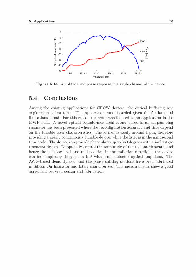
5. Applications 73
Wavelength [nm]
No
rmal
ized
tra
smis
sio
n [
dB
]
0
500
1000
1500
Ph
ase [deg
]
0
-5
-10
-15
-20
-25
-30
-351529 1529.5 1530 1530.5 1531 1531.5
Figure 5.14: Amplitude and phase response in a single channel of the device.
5.4 Conclusions
Among the existing applications for CROW devices, the optical buffering wasexplored in a first term. This application was discarded given the fundamentallimitations found. For this reason the work was focused to an application in theMWP field. A novel optical beamformer architecture based in an all-pass ringresonator has been presented where the reconfiguration accuracy and time dependon the tunable laser characteristics. The former is easily around 1 pm, thereforeproviding a nearly continuously tunable device, while the later is in the nanosecondtime scale. The device can provide phase shifts up to 360 degrees with a multistageresonator design. To optically control the amplitude of the radiant elements, andhence the sidelobe level and null position in the radiation directions, the devicecan be completely designed in InP with semiconductor optical amplifiers. TheAWG-based demultiplexer and the phase shifting sections have been fabricatedin Silicon On Insulator and lately characterized. The measurements show a goodagreement between design and fabrication.

74 5.4. Conclusions

Chapter 6
Conclusions and future work
6.1 Conclusions
The realization of all the objectives proposed at the beginning of this Ph.D. hasbeen attained with the following contributions and conclusions:
• A TMM formalism has been developed in Chapter 2 for the analysis ofCROW and SCISSOR structures. The apodization of the coupling coef-ficients in the unit cells of serial and parallel coupled resonator waveguidedevices has been introduced in section 2.3 as a mean to improve the bandpasscharacteristic of their transfer functions. The apodization of both SCISSORand CROW structures has been discussed for several windowing functionsand sidelobe/ripples suppression in both structures demonstrated respec-tively. To conclude the chapter, in section 2.4 a novel synthesis algorithmbased in the layer aggregation method has been adapted to coupled resonatoroptical waveguides. A procedure to link the contribution of each cavity to theimpulse response at every time has been derived. The procedure has beenapplied to the synthesis of CROWs, starting from targeted transfer func-tions. An excellent match between the targeted and synthesized responseshas been demonstrated for worst case convergence parameters.
• Chapter 3 reported a novel technique for controlling the coupling betweenthe resonators in CROW structures. The technique, based in a longitudinaloffset between resonators, alleviates the tight requirements in the fabricationstage typically limited by the lithographic resolution. The technique is mostsuitable for racetrack resonators given the inherent straight coupling sectionof this type of resonator. The sensitivity is increased critically by using thelongitudinal offset technique despite the increase in the footprint of the finaldevices. The technique has been introduced in section 3.2 and demonstratednumerically through BPM in section 3.3 and through TMM simulations ofseveral CROW devices in section 3.4.

76 6.2. Future work
• In chapter 4, the design, fabrication and characterization of CROW devicesimplementing the longitudinal offset technique has been presented. The de-tails of the fabrication technology are given in section 4.2. In section 4.3,the CROW devices are decomposed in its constituent parts and individuallyanalysed in detail. Finally, the results from two fabrication runs have beenpresented in section 4.4. The devices have been designed and fabricated inSilicon On Insulator through the ePIXfab platform. Both fabrication runsincluded CROW devices implementing the apodization through the longitu-dinal offset technique. In the first run the apodization is impressed over thecross coupling coefficient whilst in the second run is applied to the direct cou-pling coefficients. The results of the fabricated devices characterization havebeen compared with the theoretical predictions and are in excellent agree-ment. The technique has been patented through the Technology TransferOffice from the Universitat Politecnica de Valencia at a national level andlicensed to the UPV Spin-Off company VLC Photonics S.L.
• The last chapter of this thesis has been devoted to demonstrate the applica-tions of CROW devices given the delay and phase-shifting characteristics ofthese structures. In a first term, the delay response of the CROW deviceshas been experimentally investigated through digital signal transmission ex-periments. The results matched those previously demonstrated by the workof Vlasov et al. [9] about optical buffers employing CROW devices. The re-sults obtained showed the same limitations in terms of bandwidth and delaythat make difficult the usage of CROWs as optical buffers. At the sight ofthese results, the research was focused in the field of microwave photonics.A novel optical beamformer architecture based in all-pass ring resonatorshas been presented. The device can provide phase shifts up to 360 degreeswith a multi-stage resonator design. To optically control the amplitude ofthe radiant elements, and hence the sidelobe level and null position in theradiation directions, the device can be completely designed in InP with semi-conductor optical amplifiers. The AWG-based demultiplexer and the phaseshifting sections have been fabricated in Silicon On Insulator and lately char-acterized. The measurements show a good agreement between design andfabrication.
6.2 Future work
After the work developed in this thesis, there are some open research lines thatmay be continued:
• Study the fabrication reproducibility of the devices shown in Chapter 4:
• Within-die non-uniformity
• Non-uniformity over the wafer
• Inter-wafer non-uniformity

6. Conclusions and future work 77
• Develop robust coupling schemes tolerant to fabrication imperfections.
• Incorporate tuning elements to the CROW structures in order to compensatedeviations in fabrication.
• Test the longitudinal offset technique in different fabrication platforms.

78 6.2. Future work

Appendices


Appendix A
Integrated optics devices
modelling using High Performance
Computing and parallel Finite
Differences in the Time Domain
algorithms
The fast and efficient exchange of information in actual society is recognized asone of the most important catalysts for development.The development and socialadoption of the Internet as the principal mean for long distance fast communica-tions, is supported by ground infrastructures that mainly rely on the exchange oflight signals using optical fibers. The invention of the laser on the 60’s, enabledthe science of mastering light signals, processing and using them for ultra-long dis-tance communications. Technology developments in the field are driven by dailyincreasing demands on the amount of information to be exchanged. Therefore,telecommunication providers face the trouble of squeezing their available infras-tructure to the maximum. Moreover, more and more physical space is needed tosettle information transmitters, receivers and rely data stations, with increasingelectric power consumption. To cope this problem, the field of integrated optics [1]aims at grooming several functionalities for such data stations in the smallest spaceand with the minimum power consumption.
Integrated optics circuits are in shape devices similar to the widespread con-sumer electronics devices, as the printed circuit boards one can find inside a homecomputer. The very significant difference is that the latter use electric signals,whilst the former use optical signals to work with. This difference makes thesubject of integrated optics a complex science involving from chemical and mat-ter sciences and processes, to build the support boards for the circuits, to designengineering and signal processing to master the light therein.

82 A.1. MEEP
Amongst the required steps to produce an integrated optics component, i.e.theoretical conception, device simulation and modelling, device design, componentfabrication and characterization, device modelling plays a crucial role. The moreprecise and close to the physical phenomena taking place in these devices, themore efficient the device production cycle, from theory to availability, will be.
There is a vast variety of integrated optics devices [1], and therefore differ-ent modelling approaches [113] [114]. One of the most computationally intensiveproblems in this field is to model devices without assuming a preferential propaga-tion direction for the light signals on the devices, also known as omni-directionalpropagation. This problem is usually addressed with Finite Differences in theTime Domain (FDTD) algorithm, that solve the Maxwell equations in a givencomputational discretized cell. The FDTD algorithm calculates iteratively theelectromagnetic field components for all the computational cell points every timestep. The computational requirements for these problems depend on the size of thecell and the nature of the devices being modelled. However, the FDTD algorithmcan be parallelized, and therefore High Performance Computing (HPC) computerclusters can be used.
In this section we present the use of the FDTD software MEEP from MIT [115]applied to integrated optics devices. The modelled devices are subject of researchin our research group within several research projects.
A.1 MEEP
MEEP is an open source software FDTD project. The acronym stands for ”MITElectromagnetic Equation Propagation”. This software has been developed [115]at the Massachusetts Institute of Technology and it is maintained by Steven G.Johnson and others. Detailed information can be found in the MEEP MIT website[116]. To summarize briefly:
• Free software under the GNU/GPL.
• Simulation in 1d, 2d, 3d, and cylindrical coordinates.
• Distributed memory parallelism on any system supporting the MPI standard.
• Exploitation of symmetries to reduce the computation size.
• Arbitrary material and source distributions.
• Field analysis including flux spectra, frequency extraction, and energy inte-grals.
• Multi-parameter optimization, root-finding, integration, etcetera.
In general all the FDTD methods, and in particular MEEP, present some strengthsas its versatility and its capability to obtain the response of the system over a widerange of frequencies with a single simulation. Another advantage is the possibility

A. Integrated optics devices modelling using High Performance Computing and
parallel Finite Differences in the Time Domain algorithms 83
Structure Cell [µm] Step size [µm] # Points Memory [GB]DBR 100x5x5 0.020 3.125e8 19Ring resonator 25x20x5 0.020 3.9e8 24Grating Coupler 500x20x5 0.025 3.2e9 190
Table A.1: Memory usage of the examples.
to obtain the E and H fields everywhere in the computational cell as they evolve intime, providing animated displays of the electromagnetic field movement throughthe model that are very useful in understanding what is going on in the model,and helping to ensure that the model is working correctly.
But the FDTD methods present also some weaknesses. The main drawbackof these techniques are that, since FDTD requires that the entire computationaldomain be gridded, the grid spatial discretization must be sufficiently fine to re-solve the smallest geometrical feature in the model. This leads to very largecomputational cells which requires huge amount of computer memory and verylong simulation times. For instance, models with long, thin features, are difficultto model in FDTD because the high spatial resolution needed and the relativelylarge simulation cell leads to very long computational times and large memoryrequirements.
In order to address this very demanding computing requirements, access tohigh performance computing facilities is needed.
A.2 Computational requirements
Since the computational cell is discretized in MEEP in a two/three dimensionalmesh, the number of points in the mesh as well as the memory/process timeconsumption increases exponentially when increasing the program accuracy.
This grid of points has multiple instances during simulations and they are usedto store different parameters of the simulation as the material permittivity, electricand magnetic fields, dispersive properties of the materials, etc. Let’s assume wehave a 100x100x100 points grid. That is 1 · 106 points. Each point is stored intoa variable of type double, consuming 8 bytes, so one instance of the grid will benear 8 MB. Typically, 3D simulations keep in memory a minimum of 8 instancesof the grid, therefore the needed resources grow exponentially with the grid size.
Table A.1 shows the approximated memory usage for the examples shown inthe next section.
As described in the previous section, the FDTD method solves Maxwell equa-tions for each point in the grid on each time step. Typically, six field componentsare stored for each grid point and each field component update requires at leasteight floating point operations. Thus, a 100x100x100 grid will require 1 million ofpoints or 6 million field components. One complete update of this grid requires48.000.000 floating point operations (48 MFLOPS).

84 A.3. Usage examples
At the sight of this brief discussion, it is clear that a HPC cluster is required forthese problems for several reasons. First a single computer may have not enoughmemory to host the computational cell. Second, even in the case the problemcan be addressed with a single computer in terms of memory, the computationtime needed depends on the devices being modelled. For instance, some devicesrequire the light to recirculate several times for the final solution to converge. Andlast but not least, even in the case that computing time and memory usage couldbe copped with a single computer, a single simulation run does not happen toprovide the final results in most of the cases, therefore parameter sweeps and/oroptimization are needed, so reruns are usually performed.
A.3 Usage examples
The following examples are just a sample amongst all the problems for whichFDTD and HPC is needed for integrated optics. Thought all these problems haveanalytic models counterpart, they rely on simplifications that in most of the casesdo not hold. It is in those cases where brute force electromagnetic simulations areneeded.
A.3.1 Grating couplers
Currently, the in/out coupling of light from PIC to an optical fiber remains a seri-ous issue. The large difference in dimensions between the fiber and the waveguideson a chip causes high insertion losses and high packaging costs.
The commonly used solution to couple light into a sub-micrometer waveguide isto directly focus the beam from a lensed fiber onto the end of the sub-micrometerwaveguide at the chip edge (butt coupling). This technique introduces couplinglosses typically higher than 12 dB.
A solution to overcome this high coupling losses is to use grating couplers[117] followed by a taper to adjust the lateral size of the incident beam to thesub-micrometer waveguide width. A grating coupler is a periodic variation ofthe waveguide height along its length. Due to this variation, a fraction of thelight contained in the waveguide is radiated to the external medium. The mainadvantage of a grating coupler is the possible use of test devices everywhere onthe PIC without any cleavage.
It is interesting to improve the grating coupler design in order to maximizeits coupling efficiency [75]. For instance, there is a strong dependence betweenthe grating coupler period and the angle in which light is radiated [117]. Thisimprovement in the design can be done using a simulation tool, as the FDTDmethod provided by the MEEP software.
In Fig. A.1 a 2D view of a grating coupler is shown. The different grey levelsindicate different materials (air -white-, silica -grey- and silicon -black-). Thewaveguide is 220 nanometers height and 50 micrometers long, and the thickness

A. Integrated optics devices modelling using High Performance Computing and
parallel Finite Differences in the Time Domain algorithms 85
Figure A.1: 2D side view of a grating coupler.
Figure A.2: 2D side view of light radiated from a grating coupler with period 540 nm(top) and 640 nm (bottom).
of the substrate layers is of 2 micrometers each. The grating coupler has a periodof a few hundreds of nanometers and a depth of 70 nanometers.
In Fig. A.2 a 2D simulation of the EM fields radiated from a waveguide isshown, when the light arrives to the grating coupler. In this case, two differentgrating coupler periods have been chosen to illustrate the dependence of radiationangle on the period.
The dimensions of the 2D simulation cell are 50x10 microns and, in orderto resolve the small features of the grating coupler, the resolution value is 25nanometers. The amount of memory required to perform this simulation is ofaround 80 MB, and it takes around 10 minutes in a modest HPC cluster made upof 10 nodes.
This 2D simulation provides the designer a basic understanding about the be-haviour of the device. However, in order to get a complete understanding of thedevice performance, a more realistic 3D simulation has to be carried out. In thiscase, the effect of the taper that adiabatically couples the light from the waveg-uide to the grating coupler must be included, so the dimensions of the simulationcell are increased up to 500x20x5 microns. For the same value of the resolution(25 nanometers), around 190 GB of memory is required, even exploiting the cellsymmetries to reduce the computation size. So, in order to perform this kind ofintensive simulations, the use of larger HPC cluster resources is needed.
A.3.2 Ring Resonators
An integrated optics ring resonator consists of a waveguide in a closed loop coupledto one or more input/output (or bus) waveguides as shown in Fig. A.3. Dependingon the wavelength of the light and input waveguide used, constructive interference

86 A.3. Usage examples
Figure A.3: 3D model of a ring resonator.
of the multiple round-trips within the ring happens at different output waveguides.
Devices composed of single or multiple micro ring resonator cavities can be ex-ploited in a wide variety of classical applications including, amongst other: channelfiltering in WDM systems [6], linear and nonlinear digital optics [8], optical buffer-ing [51] and modulation [10], dispersion compensation [11], switching [12]. Fur-thermore, the range of applications can be extended to encompass the emergentfield of quantum information processing [4]. Fig. A.4 shows a two-dimensionalslice with a graphical representation of the electromagnetic fields inside the res-onator. This problem was addressed with an HPC cluster with 100 nodes, cell sizeof 25x20x5 microns, grid resolution of 20 nanometers, total memory usage of 24GB and solved in 59 hours.
Distributed Bragg Reflectors
Distributed Bragg Reflectors (DBRs) [118] in integrated optics are similar to FiberBragg Gratings (FBGs) [119] in optical fibers. These are key devices in opticalnetworking, and used in a vast number of applications, ranging from simple WDMmulti/demultiplexer to dispersion compensation. FBGs gratings are built in opti-cal fibers by changing the refractive index in the core of fiber in a periodic fashion.The DBR is the integrated optics counterpart, and can be either a waveguidewhose width is changed periodically between two values (uniform) or following agiven pattern (apodized). Two examples of these are illustrated in Fig. A.5. OtherDBRs are built keeping the waveguide width constant and slicing the waveguide

A. Integrated optics devices modelling using High Performance Computing and
parallel Finite Differences in the Time Domain algorithms 87
Figure A.4: Electromagnetic field representation in a racetrack resonator.
Figure A.5: Uniform and apodized DBRs.
vertically. When the slices do not go all through the waveguide height, FDTD isa handy and powerful tool to solve the problem, since an analytic approach mightbe complex and not precise. Fig. A.6 shows the spectral response of both uniformand apodized DBR filters calculated with MEEP. This problem was address withan HPC cluster with 50 nodes, cell size of 100x5x5 microns, grid resolution of 20nanometers, total memory usage of 19 GB and solved in 30 hours.

88 A.3. Usage examples
1.54 1.545 1.55 1.555 1.56 1.565 1.57 1.575 1.58 1.585 1.59 1.595 1.6−35
−33
−31
−29
−27
−25
−23
−21
−19
−17
−15
−13
−11
−9
−7
−5
−3
−10
Wavelength (um)
Nor
mal
ized
Am
plitu
de (
dB)
Uniform Grating vs Apodized grating (Reflection)
Figure A.6: Reflection spectrum of a uniform (red) and apodized (blue) DBR.

Appendix B
Characterization setup
The characterization of the fabricated devices was carried out in the facilities of theOptical and Quantum Communications Group from the Universitat Politecnica deValencia. The laboratory is equipped with state-of-the-art optical instrumentationas well as for RF. The bare-die characterization systems available at the timethis thesis was written, allowed for butt-coupled chips characterization but notfor vertical in/out coupling. In order to characterize the SOI devices providedwith grating couplers, a vertical fiber setup was assembled. The reference setupemployed was the one from the imec group from University of Gent in Belgium.The schematic of the setup is shown in Fig.B.1.
The setup, placed on top of a suspended table that absorbs the vibrationsand eases the placement of components, will be detailed part by part. The mostimportant components are pair of 3-axis nanopositioning stages as shown in Fig.B.3 where custom 10 degrees angled supports where placed. The fibers must havean inclination of 10 degrees with respect to vertical in order to maximize thecoupling efficiency to the grating couplers and to minimize reflections into thefibers. This two stages will hold and position the input and output fiber with therequired accuracy on top on the chip. In the middle of this two stages, another3-axis stage was located in order to place the chip and it is shown in Fig. B.4. Thechips are mounted on top of a vacuum chuck to avoid vibrations and undesiredmovements of the chips while performing the characterization.
To place the fibers in the appropriate position of the grating couplers, a micro-scope camera was added to the system (Fig.B.6). This vision system is comprisedof a common CCTV color camera with an extension tube and a microscope objec-tive chosen appropriately to provide the system the required magnification. TheField of View (FOV) of the system is approximately 500 x 800 microns. The visionsystem includes a 3 axis motorized stage for the displacement of the camera overthe chip under test. The last component of the vision system is an LCD monitorplaced inside the setup and used to show the camera images. In Fig.B.7 the imageof a chip and the input and output fiber placed on top of it is shown. The inclina-

90
TUNABLE
LASER
GPIB INTERFACE
MEASUREMENT AND
CONTROL SOFTWAREMICROSCOPE
CAMERA
LAMP
POLARIZATION
CONTROL
INPUT FIBER
OUTPUT
FIBER
POWER
METER
TRANSLATION STAGES
RAILSUSPENDED TABLE
Figure B.1: Vertical fiber setup schematic
tion of the camera and the illumination system allows for an easy alignment in thevertical axis. The fibers produce a shadow that can be used as a reference in thevertical plane. When the fiber and its shadow are coincident, one can assume thatthe height is the appropriate for the measure, meaning that the fiber is almosttouching the surface of the chip.
Every nanopositiong stage is mounted on top of rail to facilitate the movementand ensure the alignment of the different positioners. The full assembled setup isshown in Fig.B.2. All the components are assembled into a clean vault in orderto keep dust clean the system. Also reduces the fiber vibrations induced by aircurrents. Fig.B.5 shows a closer look to the fibers located on top of the chip forthe characterization.
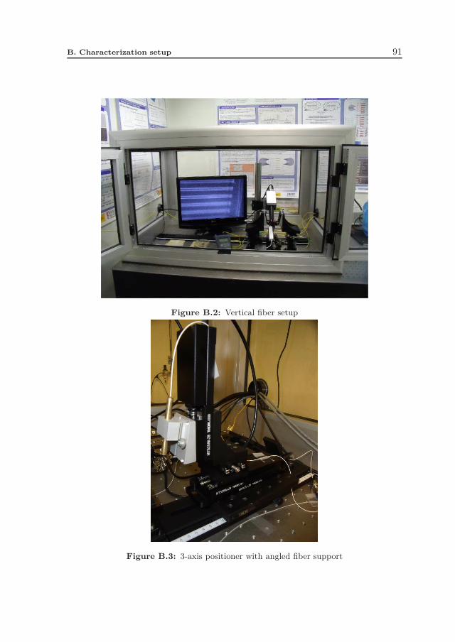
B. Characterization setup 91
Figure B.2: Vertical fiber setup
Figure B.3: 3-axis positioner with angled fiber support

92
Figure B.4: Vacuum chuck
Figure B.5: Detail of the vertical fibers coupled to the chip

B. Characterization setup 93
Figure B.6: Video camera with microscope objective
Figure B.7: LCD monitor showing the chip and fiber images.

94

Appendix C
List of publications
C.1 SCI Journal papers
1. J. Capmany, P. Munoz, J. D. Domenech, and M. A. Muriel, “Apodized cou-pled resonator waveguides,” Optics Express, vol. 15, no. 16, pp. 10196–10206,2007.
2. J. D. Domenech, P. Munoz, and J. Capmany, “The longitudinal offset tech-nique for apodization of coupled resonator optical waveguide devices: con-cept and fabrication tolerance analysis,” Optics Express, vol. 17, no. 23,pp. 21050–21059, 2009.
3. P. Munoz, J. D. Domenech, and J. Capmany, “Synthesis of coupled resonatoroptical waveguides by cavity aggregation,” Optics Express, vol. 18, no. 2,pp. 1600–160, 2010.
4. J. D. Domenech, P. Munoz, and J. Capmany, “Transmission and group-delaycharacterization of coupled resonator optical waveguides apodized throughthe longitudinal offset technique,” Optics Letters, vol. 36, pp. 136–138, 2011.
5. P. Munoz, R. Garcia-Olcina, C. Habib, L. R. Chen, X. J. M. Leijtens,J. D. Domenech, M. Rius, J. Capmany, T. De Vries, M. J. R. Heck, L. Au-gustin, R. Notzel, and D. Robbins, “Multi-wavelength laser based on anArrayed Waveguide Grating and Sagnac loop reflectors monolithically inte-grated on InP,” IET Optoelectronics, vol. 5, 2011.
6. E. Xifre, J. D. Domenech, R. Fenollosa, P. Munoz, J. Capmany, and F. Meseguer,“All silicon waveguide spherical microcavity device,” Optics Express, vol. 19,pp. 3185–3192, 2011.
7. J. S. Fandino, J. D. Domenech, P. Munoz, and J. Capmany, “IntegratedInP frequency discriminator for Phase-modulated microwave photonic links,”Opt. Express, vol. 21, pp. 3726–3736, Feb 2013.

96 C.2. Conference papers
C.2 Conference papers
1. P. Munoz, J. D. Domenech, M. D. Manzanedo, J. H. den Besten, and J. Cap-many, “Design of arrayed waveguide sagnac interferometers for OTDM-WDM optical networks,” in Proc. of the V Reunion Espanola de Opto-electronica, OPTOEL 2007, pp. 99–104, 2007.
2. J. D. Domenech, P. Munoz, and J. Capmany, “Apodized chirped coupledresonator optical waveguides,” in Proc. of the 10th anniversary internationalconference on transparent optical networks, ICTON, Vol. 4, pp. 250–253,2008.
3. J. D. Domenech, R. Garcia-Olcina, P. Munoz, and J. Capmany, “Integratedoptics devices modelling using High Performance Computing and parallelFinite Differences in the Time Domain algorithms,” in Proc. of the 3rdIberian Grid Infrastructure Conference, IBERGRID 2009, pp. 1–9, 2009.
4. J. D. Domenech, P. Munoz, and J. Capmany, “Tunable microwave photoniphase shifter using an all-pass ring resonator filter,” in Proc. of the VIReunion Espanola de Optoelectronica, OPTOEL 2009, pp. 159–163, 2009.
5. R. Garcia-Olcina, J. D. Domenech, P. Munoz, and J. Capmany, “Apodi-zed grating couplers in Silicon-On-Insulator,” in Proc. of the VI ReunionEspanola de Optoelectronica, OPTOEL 2009, pp. 65–68, 2009.
6. P. Munoz, R. Garcia-Olcina, J. D. Domenech, M. Rius, J. Capmany, L. R.Chen, C. Habib, X. J. M. Leijtens, T. de Vries, M. J. R. Heck, L. M. Augustin,R. Notzel, and D. J. Robbins, “Multi-wavelength laser based on an arrayedwaveguide grating and Sagnac loop reflectors monolithically integrated onInP,” in Proc. Of the European Conference on Integrated Optics (ECIO),Cambridge,(U.K.), 2010.
7. J. D. Domenech, M. Rius, J. Mora, P. Munoz, and J. Capmany, “Microwavephotonics beamformer based on ring resonators and arrayed waveguide grat-ings,” in Proc. Of the European Conference on Integrated Optics (ECIO),Cambridge,(U.K.), 2010.
8. P. Munoz, R. Garcia-Olcina, J. D. Domenech, M. Rius, J. Sancho, J. Cap-many, L. R. Chen, C. Habib, X. J. M. Leijtens, T. de Vries, M. J. R. Heck,L. M. Augustin, R. Notzel, and D. J. Robbins, “InP monolithically integratedlabel swapper device for spectral amplitude coded optical packet networks,”in Postdealine Paper, presented at the European Conference on Integratedoptics ECIO 2010, Cambridge, UK, 2010.
9. J. D. Domenech, M. Rius, P. Munoz, and J. Capmany, “Apodized cou-pled resonator optical waveguides using the longitudinal offset technique,”in Proc. of the European Conference on Integrated Optics (ECIO), Cam-bridge,(U.K.), 2010.

C. List of publications 97
10. E. Xifre, R. Fenollosa, J. D. Domenech, M. Rius, P. Munoz, J. Capmany, andF. Meseguer, “All silicon waveguide spherical microcavity device,” in Proc.Of the European Conference on Integrated optics (ECIO), Cambridge,(U.K.),2010.
11. J. D. Domenech, P. Munoz, and J. Capmany, “Apodization of coupled res-onator optical waveguide devices through a longitudinal offset technique,” inProc. of the SPIE Photonics Europe 2010, Brussels,(BE), 2010.
12. J. D. Domenech, P. Munoz, and J. Capmany, “Discretely tunable microwavephotonics beamformer based on ring resonators and arrayed waveguide grat-ings,” in Proc. of the SPIE Photonics Europe 2010, Brussels,(BE), 2010.
13. J. D. Domenech, P. Munoz, and J. Capmany, “Experimental demonstrationof the longitudinal offset technique for the apodization of coupled resonatoroptical waveguide devices,” in Lasers and Electro-Optics/Quantum Electron-ics and Laser Science Conference: 2010 Laser Science to Photonic Applica-tions, CLEO/QELS 2010, art. no. 5500898, (2010), 2010.
14. E. Xifre, J. D. Domenech, R. Fenollosa, P. Munoz, J. Capmany, and F. Meseguer,“Add-drop filter based on silicon spherical microcavities,” in ConferenciaEspanola de Nanofotonica (CEN 2010), 2010.
15. J. D. Domenech, P. Munoz, R. Garcia-Olcina, X. Leijtens, D. Robbins, T. Vries,and J. Capmany, “Design and fabrication of a narrow band phase shift en-abled optical beamformer monolithically integrated on InP,” in Proc. of theVII Reunion Espanola de Optoelectronica, OPTOEL 2011, pp. 1–4, 2011.
16. J. D. Domenech, P. Munoz, I. Artundo, J. Capmany, P. Dumon, and W. Bo-gaerts, “Design, fabrication and characterization of a narrow bandwidth mi-crowave photonics beamformer in a SOI platform,” in Proc. of the 16thEuropean Conference on Integrated Optics (ECIO), Sitges,(Spain), 2012.
17. J. S. Fandino, J. D. Domenech, P. Munoz, and J. Capmany, “Design andexperimental characterization of an InP photonic integrated circuit workingas a receiver for frequency-modulated direct-detection microwave photoniclinks,” in Proc. of SPIE Integrated Optics: Devices, Materials, and Tech-nologies XVII, pp. 862708–862708–8, 2013.
C.3 Papers in other journals
1. P. Munoz, J. D. Domenech, . Zheng Lu, C. Habib, and J. Capmany, “Multi-functional optical devices and subsystems integrated on a chip,” Waves,vol. 1, 2009.

98 C.3. Papers in other journals
2. P. Munoz, J. D. Domenech, A. I, C. Habib, X. J. M. Leijtens, T. De Vries,D. Robbins, J. H. Den Besten, L. R. Chen, and J. Capmany, “Applica-tion specific photonic integrated circuits through generic integration, a novelparadigm in photonics,” Waves, vol. 3, 2011.

Bibliography
[1] R. G. Hunsperger, Integrated Optics. Springer Verlag, 5th ed., September2002.
[2] C. Dragone, “An N*N optical multiplexer using a planar arrangement of twostar couplers,” Photonics Technology Letters, vol. 3, pp. 812–815, Sept. 1991.
[3] B. Little, S. Chu, H. Haus, J. Foresi, and J.-P. Laine, “Microring resonatorchannel dropping filters,” Journal of Lightwave Technology, vol. 15, pp. 998–1005, June 1997.
[4] K. Vahala, “Optical microcavities,” Nature, vol. 424, pp. 839–846, 2003.
[5] C. K. Madsen and G. Lenz, “Optical all-pass filters for phase response designwith applications for dispersion compensation,” IEEE Photonics TechnologyLetters, vol. 10, pp. 994–996, July 1998.
[6] J. Capmany and M. Muriel, “A new transfer matrix formalism for the anal-ysis of fiber ring resonators: compound coupled structures for FDMA de-multiplexing,” Journal of Lightwave Technology, vol. 8, pp. 1904–1919, Dec.1990.
[7] J. Lloret, J. Sancho, M. Pu, I. Gasulla, K. Yvind, S. Sales, and J. Capmany,“Tunable complex-valued multi-tap microwave photonic filter based on singlesilicon-on-insulator microring resonator,” Opt. Express, vol. 19, pp. 12402–12407, Jun 2011.
[8] V. Van, T. Ibrahim, P. Absil, F. Johnson, R. Grover, and P.-T. Ho, “Opticalsignal processing using nonlinear semiconductor microring resonators,” Se-lected Topics in Quantum Electronics, IEEE Journal of, vol. 8, pp. 705–713,May/Jun 2002.
[9] F. Xia, L. Sekaric, and Y. Vlasov, “Ultra compact optical buffers on a siliconchip,” Nature Photonics, vol. 1, pp. 65–71, 2007.

100 Bibliography
[10] H. Tazawa and W. Steier, “Analysis of ring resonator-based traveling-wavemodulators,” Photonics Technology Letters, IEEE, vol. 18, pp. 211–213, 1,2006.
[11] C. Madsen, G. Lenz, A. Bruce, M. Cappuzzo, L. Gomez, and R. Scotti,“Integrated all-pass filters for tunable dispersion and dispersion slope com-pensation,” Photonics Technology Letters, IEEE, vol. 11, pp. 1623–1625, Dec1999.
[12] B. Little, S. Chu, W. Pan, and Y. Kokubun, “Microring resonator arrays forVLSI photonics,” Photonics Technology Letters, IEEE, vol. 12, pp. 323–325,Mar 2000.
[13] J. E. Heebner, R. W. Boyd, and Q.-H. Park, “SCISSOR solitons and othernovel propagation effects in microresonator-modified waveguides,” J. Opt.Soc. Am. B, vol. 19, no. 4, pp. 722–731, 2002.
[14] A. Yariv, Y. Xu, R. K. Lee, and A. Scherer, “Coupled-resonator opticalwaveguide: a proposal and analysis,” Optics Letters, vol. 24, no. 11, pp. 711–713, 1999.
[15] P. Cross and H. Kogelnik, “Sidelobe supression in corrugated-waveguide fil-ters,” Optics letters, vol. 1, pp. 43–45, 1977.
[16] E. Wooten, K. Kissa, A. Yi-Yan, E. Murphy, D. Lafaw, P. Hallemeier,D. Maack, D. Attanasio, D. Fritz, G. McBrien, and D. Bossi, “A reviewof lithium niobate modulators for fiber-optic communications systems,” Se-lected Topics in Quantum Electronics, IEEE Journal of, vol. 6, no. 1, pp. 69–82, 2000.
[17] G. Maxwell and B. J. Ainslie, “Demonstration of a directly written direc-tional coupler using uv-induced photosensitivity in a planar silica waveg-uide,” Electronics Letters, vol. 31, no. 2, pp. 95–96, 1995.
[18] Y. Hibino, F. Hanawa, H. Nakagome, M. Ishii, and N. Takato, “High reli-ability optical splitters composed of silica-based planar lightwave circuits,”Lightwave Technology, Journal of, vol. 13, no. 8, pp. 1728–1735, 1995.
[19] Y. Hibino, T. Kitagawa, K. Hill, F. Bilodeau, B. Malo, J. Albert, andD. Johnson, “Wavelength division multiplexer with photoinduced bragg grat-ings fabricated in a planar-lightwave-circuit-type asymmetric mach-zehnderinterferometer on si,” Photonics Technology Letters, IEEE, vol. 8, no. 1,pp. 84–86, 1996.
[20] H. Takahashi, S. Suzuki, K. Kato, and I. Nishi, “Arrayed-waveguide grat-ing for wavelength division multi/demultiplexer with nanometre resolution,”Electronics letters, vol. 26, no. 2, pp. 87–88, 1990.

Bibliography 101
[21] X. Duan, Y. Huang, Y. Cui, J. Wang, and C. M. Lieber, “Indium phosphidenanowires as building blocks for nanoscale electronic and optoelectronic de-vices,” Nature, vol. 409, no. 6816, pp. 66–69, 2001.
[22] R. Nagarajan and M. Smit, “Photonic integration,” IEEE LEOS Newsletter,vol. 21, no. 3, pp. 4–10, 2007.
[23] G. T. Reed, Silicon Photonics: The State of the Art. John Wiley & Sons,Ltd, 2008.
[24] “ePIXfab, the European Silicon Photonics Platform.”http://www.epixfab.eu/.
[25] “Optoelectronic System Integration in Silicon.” http://opsisfoundry.org/.
[26] “Joint European Platform for InP-based Photonic Integrated Componentsand Circuits (JePPIX)..” http://www.jeppix.eu/.
[27] “LioniX, microfluidics and integrated optics.” http://www.lionixbv.nl/.
[28] “PhoeniX B.V, solutions for micro and nano technologies.”http://www.phoenixbv.com/.
[29] “Interuniversity microelectronics centre.” http://www.imec.be/.
[30] “Laboratoire d’electronique des technologies de l’information.” http://www-leti.cea.fr/.
[31] “IHP - Innovations for High Performance Microelectronics.” http://www.ihp-microelectronics.com/.
[32] A. Oppenheim, R. Schafer, and J. Buck, Discrete-time signal processing.Prentice-Hall, 1999.
[33] D. Pastor, J. Capmany, B. Ortega, V. Tatay, and J. Marti, “Design ofapodised linearly chirped fiber gratings for dispersion compensation,” Jour-nal of Lightwave Technology, vol. 14, pp. 2581–2588, 1996.
[34] J. Capmany, M. Muriel, and S. Sales, “Highly accurate synthesis of fiber andwaveguide Bragg gratings by an impedance reconstruction layer-aggregationmethod,” Quantum Electronics, IEEE Journal of, vol. 43, pp. 889–898, Oct.2007.
[35] S. Somekh, E. Garmire, A. Yariv, H. Garvin, and R. Hunsperger, “Chan-nel optical waveguide directional couplers,” Applied Physics Letters, vol. 22,no. 1, pp. 46–47, 1973.
[36] A. Yariv, “Universal relations for coupling of optical power between mi-croresonators and dielectric waveguides,” Electronics Letters, vol. 36, no. 4,pp. 321–322, 2000.
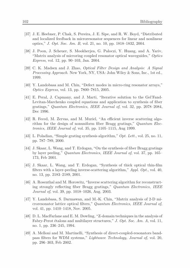
102 Bibliography
[37] J. E. Heebner, P. Chak, S. Pereira, J. E. Sipe, and R. W. Boyd, “Distributedand localized feedback in microresonator sequences for linear and nonlinearoptics,” J. Opt. Soc. Am. B, vol. 21, no. 10, pp. 1818–1832, 2004.
[38] J. Poon, J. Scheuer, S. Mookherjea, G. Paloczi, Y. Huang, and A. Yariv,“Matrix analysis of microring coupled resonator optical waveguides,” OpticsExpress, vol. 12, pp. 90–103, Jan. 2004.
[39] C. K. Madsen and J. Zhao, Optical Filter Design and Analysis: A SignalProcessing Approach. New York, NY, USA: John Wiley & Sons, Inc., 1st ed.,1999.
[40] Y. Landobasa and M. Chin, “Defect modes in micro-ring resonator arrays,”Optics Express, vol. 13, pp. 7800–7815, 2005.
[41] E. Peral, J. Capmany, and J. Marti, “Iterative solution to the Gel’Fand-Levitan-Marchenko coupled equations and application to synthesis of fibergratings,” Quantum Electronics, IEEE Journal of, vol. 32, pp. 2078–2084,Dec 1996.
[42] R. Feced, M. Zervas, and M. Muriel, “An efficient inverse scattering algo-rithm for the design of nonuniform fiber Bragg gratings,” Quantum Elec-tronics, IEEE Journal of, vol. 35, pp. 1105–1115, Aug 1999.
[43] L. Poladian, “Simple grating synthesis algorithm,” Opt. Lett., vol. 25, no. 11,pp. 787–789, 2000.
[44] J. Skaar, L. Wang, and T. Erdogan, “On the synthesis of fiber Bragg gratingsby layer peeling,” Quantum Electronics, IEEE Journal of, vol. 37, pp. 165–173, Feb 2001.
[45] J. Skaar, L. Wang, and T. Erdogan, “Synthesis of thick optical thin-filmfilters with a layer-peeling inverse-scattering algorithm,” Appl. Opt., vol. 40,no. 13, pp. 2183–2189, 2001.
[46] A. Rosenthal and M. Horowitz, “Inverse scattering algorithm for reconstruct-ing strongly reflecting fiber Bragg gratings,” Quantum Electronics, IEEEJournal of, vol. 39, pp. 1018–1026, Aug. 2003.
[47] Y. Landobasa, S. Darmawan, and M.-K. Chin, “Matrix analysis of 2-D mi-croresonator lattice optical filters,” Quantum Electronics, IEEE Journal of,vol. 41, pp. 1410–1418, Nov. 2005.
[48] D. L. MacFarlane and E. M. Dowling, “Z-domain techniques in the analysis ofFabry-Perot etalons and multilayer structures,” J. Opt. Soc. Am. A, vol. 11,no. 1, pp. 236–245, 1994.
[49] A. Melloni and M. Martinelli, “Synthesis of direct-coupled-resonators band-pass filters for WDM systems,” Lightwave Technology, Journal of, vol. 20,pp. 296–303, Feb 2002.

Bibliography 103
[50] R. Orta, P. Savi, R. Tascone, and D. Trinchero, “Synthesis of multiple-ring-resonator filters for optical systems,” Photonics Technology Letters, IEEE,vol. 7, pp. 1447–1449, Dec. 1995.
[51] F. Xia, M. Rooks, L. Sekaric, and Y. Vlasov, “Ultra-compact high order ringresonator filters using submicron silicon photonic wires for on-chip opticalinterconnects,” Optics Express, vol. 15, no. 19, pp. 11934–11941, 2007.
[52] K. Ebeling, Integrated Optoelectronics. Springer-Verlag, 1993.
[53] H. Yamada, T. Chu, S. Ishida, and Y. Arakawa, “Si photonic wire waveguidedevices,” Selected Topics in Quantum Electronics, IEEE Journal of, vol. 12,no. 6, pp. 1371–1379, 2006.
[54] Y. Shi, S. He, and S. Anand, “Ultracompact directional couplers realized ininp by utilizing feature size dependent etching,” Opt. Lett., vol. 33, pp. 1927–1929, Sep 2008.
[55] F. Xia, L. Sekaric, and Y. A. Vlasov, “Mode conversion losses in silicon-on-insulator photonic wire based racetrack resonators,” Optics Express, vol. 14,no. 9, pp. 3872–3886, 2006.
[56] A. Yen, A. Tritchkov, J. P. Stirniman, G. Vandenberghe, R. Jonckheere,K. Ronse, and L. Van den hove, “Characterization and correction of opticalproximity effects in deep ultraviolet lithography using behavior modeling,”Journal of Vacuum Science Technology B: Microelectronics and NanometerStructures, vol. 14, no. 6, pp. 4175–4178, 1996.
[57] M. Popovic, C. Manolatou, and M. Watts, “Coupling-induced resonance fre-quency shifts in coupled dielectric multi-cavity filters,” Opt. Express, vol. 14,pp. 1208–1222, Feb 2006.
[58] S. Selvaraja, W. Bogaerts, P. Dumon, D. Van Thourhout, and R. Baets,“Subnanometer linewidth uniformity in silicon nanophotonic waveguide de-vices using cmos fabrication technology,” Selected Topics in Quantum Elec-tronics, IEEE Journal of, vol. 16, no. 1, pp. 316–324, 2010.
[59] W. Bogaerts, R. Baets, P. Dumon, V. Wiaux, S. Beckx, D. Taillaert, B. Luys-saert, J. V. Campenhout, P. Bienstman, and D. V. Thourhout, “Nanopho-tonic waveguides in Silicon-on-Insulator fabricated with CMOS technology,”Journal of Lightwave Technology, vol. 23, no. 1, p. 401, 2005.
[60] K. Saitoh and M. Koshiba, “Full-vectorial finite element beam propagationmethod with perfectly matched layers for anisotropic optical waveguides,”J. Lightwave Technol., vol. 19, p. 405, Mar 2001.
[61] D. Geuzebroek and A. Driessen, Ring-Resonator-Based Wavelength Filters,vol. 123 of Springer Series in Optical Sciences. Springer Berlin Heidelberg,2006.

104 Bibliography
[62] W. W. Hu, K. Sarveswaran, M. Lieberman, and G. H. Bernstein,“Sub-10 nm electron beam lithography using cold development ofpoly(methylmethacrylate),” Journal of Vacuum Science & Technology B:Microelectronics and Nanometer Structures, vol. 22, no. 4, pp. 1711–1716,2004.
[63] T. Barwicz, M. A. Popovic, M. R. Watts, P. T. Rakich, E. P. Ippen, andH. I. Smith, “Fabrication of add-drop filters based on frequency-matchedmicroring resonators,” J. Lightwave Technol., vol. 24, p. 2207, May 2006.
[64] S. Selvaraja, P. Jaenen, W. Bogaerts, D. Van Thourhout, P. Dumon, andR. Baets, “Fabrication of photonic wire and crystal circuits in Silicon-on-Insulator using 193-nm optical lithography,” Lightwave Technology, Journalof, vol. 27, no. 18, pp. 4076–4083, 2009.
[65] T. Spuesens, L. Liu, T. De Vries, P. Romeo, P. Regreny, andD. Van Thourhout, “Improved design of an inp-based microdisk laser het-erogeneously integrated with SOI,” in Group IV Photonics, 2009. GFP 09.6th IEEE International Conference on, pp. 202–204, 2009.
[66] K. Yamada, Silicon Photonic Wire Waveguides: Fundamentals and Appli-cations, vol. 119 of Topics in Applied Physics. Springer Berlin Heidelberg,2011.
[67] P. Dumon, W. Bogaerts, V. Wiaux, J. Wouters, S. Beckx, J. Van Camp-enhout, D. Taillaert, B. Luyssaert, P. Bienstman, D. Van Thourhout, andR. Baets, “Low-loss soi photonic wires and ring resonators fabricated withdeep uv lithography,” Photonics Technology Letters, IEEE, vol. 16, no. 5,pp. 1328–1330, 2004.
[68] S. Lardenois, D. Pascal, L. Vivien, E. Cassan, S. Laval, R. Orobtchouk,M. Heitzmann, N. Bouzaida, and L. Mollard, “Low-loss submicrometersilicon-on-insulator rib waveguides and corner mirrors,” Opt. Lett., vol. 28,pp. 1150–1152, Jul 2003.
[69] Q. Xu, D. Fattal, and R. G. Beausoleil, “Silicon microring resonators with1.5-µm radius,” Opt. Express, vol. 16, pp. 4309–4315, Mar 2008.
[70] K. D. Vos, I. Bartolozzi, E. Schacht, P. Bienstman, and R. Baets, “Silicon-on-insulator microring resonator forsensitive and label-free biosensing,” Opt.Express, vol. 15, pp. 7610–7615, Jun 2007.
[71] “MPB, The MIT Photonic Bands.” http://ab-initio.mit.edu/wiki/index.php/MIT Photonic Bands.
[72] E. Dulkeith, F. Xia, L. Schares, W. M. J. Green, and Y. A. Vlasov, “Groupindex and group velocity dispersion in silicon-on-insulator photonic wires,”Opt. Express, vol. 14, no. 9, pp. 3853–3863, 2006.

Bibliography 105
[73] S. Darmawan and M. K. Chin, “Critical coupling, oscillation, reflection, andtransmission in optical waveguide-ring resonator systems,” J. Opt. Soc. Am.B, vol. 23, pp. 834–841, May 2006.
[74] R. Fortenberry, “Enhanced wavelength resolution chromatic dispersion mea-surements using fixed sideband technique,” in Optical Fiber CommunicationConference, 2000, vol. 1, pp. 107–109 vol.1, 2000.
[75] D. Taillaert, F. V. Laere, M. Ayre, W. Bogaerts, D. V. Thourhout, P. Bien-stman, and R. Baets, “Grating couplers for coupling between optical fibersand nanophotonic waveguides,” Japanese Journal of Applied Physics, vol. 45,no. 8A, pp. 6071–6077, 2006.
[76] J. Capmany, P. Munoz, J. D. Domenech, and M. A. Muriel, “Apodizedcoupled resonator waveguides,” Optics Express, vol. 15, pp. 10196–10206,Aug. 2007.
[77] F. Morichetti, A. Canciamilla, M. Martinelli, A. Samarelli, R. M. D. L. Rue,M. Sorel, and A. Melloni, “Coherent backscattering in optical microringresonators,” Applied Physics Letters, vol. 96, no. 8, p. 081112, 2010.
[78] J. Scheuer, J. K. S. Poon, G. T. Paloczi, and A. Yariv, “Coupled resonatoroptical waveguides (crow),” Proc. SPIE 5735, Advanced Optical and Quan-tum Memories and Computing II, pp. 52–59, 2005.
[79] R. Tucker, P.-C. Ku, and C. Chang-Hasnain, “Slow-light optical buffers:capabilities and fundamental limitations,” Lightwave Technology, Journalof, vol. 23, no. 12, pp. 4046–4066, 2005.
[80] N. Fontaine, J. Yang, Z. Pan, S. Chu, W. Chen, B. E. Little, and S. J. B.Yoo, “Continuously tunable optical buffering at 40 gb/s for optical packetswitching networks,” J. Lightwave Technol., vol. 26, pp. 3776–3783, Dec2008.
[81] L. Y. Mario and M. K. Chin, “Optical buffer with higher delay-bandwidthproduct in a two-ring system,” Opt. Express, vol. 16, pp. 1796–1807, Feb2008.
[82] J. Capmany and D. Novak, “Microwave photonics combines two worlds,”Nature Photonics, vol. 1, pp. 319–330, 2007.
[83] D. Marpaung, C. Roeloffzen, R. Heideman, A. Leinse, S. Sales, andJ. Capmany, “Integrated microwave photonics,” Laser & Photonics Reviews,pp. n/a–n/a, 2013.
[84] R. Adar, M. Serbin, and V. Mizrahi, “Less than 1 db per meter propaga-tion loss of silica waveguides measured using a ring resonator,” LightwaveTechnology, Journal of, vol. 12, no. 8, pp. 1369–1372, 1994.

106 Bibliography
[85] B. Howley, Y. Chen, X. Wang, Q. Zhou, Z. Shi, Y. Jiang, and R. T. Chen,“2-bit reconfigurable true time delay lines using 2× 2 polymer waveguideswitches,” Photonics Technology Letters, IEEE, vol. 17, no. 9, pp. 1944–1946, 2005.
[86] G. Lenz, B. Eggleton, C. K. Madsen, and R. Slusher, “Optical delay linesbased on optical filters,” Quantum Electronics, IEEE Journal of, vol. 37,no. 4, pp. 525–532, 2001.
[87] M. Rasras, C. Madsen, M. Cappuzzo, E. Chen, L. Gomez, E. Laskowski,A. Griffin, A. Wong-Foy, A. Gasparyan, A. Kasper, J. Le Grange, and S. Pa-tel, “Integrated resonance-enhanced variable optical delay lines,” PhotonicsTechnology Letters, IEEE, vol. 17, no. 4, pp. 834–836, 2005.
[88] L. Zhuang, C. G. H. Roeloffzen, R. Heideman, A. Borreman, A. Meijerink,and W. van Etten, “Single-chip ring resonator-based 1 times; 8 optical beamforming network in cmos-compatible waveguide technology,” Photonics Tech-nology Letters, IEEE, vol. 19, no. 15, pp. 1130–1132, 2007.
[89] A. Melloni, F. Morichetti, C. Ferrari, and M. Martinelli, “Continuouslytunable 1 byte delay in coupled-resonator optical waveguides,” Opt. Lett.,vol. 33, pp. 2389–2391, Oct 2008.
[90] J. Cardenas, M. A. Foster, N. Sherwood-Droz, C. B. Poitras, H. L. R. Lira,B. Zhang, A. L. Gaeta, J. B. Khurgin, P. Morton, and M. Lipson, “Wide-bandwidth continuously tunable optical delay line using silicon microringresonators,” Opt. Express, vol. 18, pp. 26525–26534, Dec 2010.
[91] P. Morton, J. Cardenas, J. Khurgin, and M. Lipson, “Fast thermal switch-ing of wideband optical delay line with no long-term transient,” PhotonicsTechnology Letters, IEEE, vol. 24, no. 6, pp. 512–514, 2012.
[92] Q. Chang, Q. Li, Z. Zhang, M. Qiu, T. Ye, and Y. Su, “A tunable broadbandphotonic rf phase shifter based on a silicon microring resonator,” PhotonicsTechnology Letters, IEEE, vol. 21, no. 1, pp. 60–62, 2009.
[93] W. Xue, S. Sales, J. Capmany, and J. Mørk, “Microwave phase shifter withcontrollable power response based on slow-and fast-light effects in semicon-ductor optical amplifiers,” Optics letters, vol. 34, no. 7, pp. 929–931, 2009.
[94] W. Xue, S. Sales, J. Capmany, and J. Mørk, “Wideband 360 microwave pho-tonic phase shifter based on slow light in semiconductor optical amplifiers,”Opt. Express, vol. 18, no. 6, pp. 6156–6163, 2010.
[95] J. Lloret, G. Morthier, F. Ramos, S. Sales, D. V. Thourhout, T. Spuesens,N. Olivier, J.-M. Fedeli, and J. Capmany, “Broadband microwave pho-tonic fully tunable filter using a single heterogeneously integrated iii-v/soi-microdisk-based phase shifter,” Opt. Express, vol. 20, pp. 10796–10806, May2012.

Bibliography 107
[96] P. Morton and J. Khurgin, “Microwave photonic delay line with separatetuning of the optical carrier,” Photonics Technology Letters, IEEE, vol. 21,no. 22, pp. 1686–1688, 2009.
[97] S. Chin, L. Thevenaz, J. Sancho, S. Sales, J. Capmany, P. Berger, J. Bour-derionnet, and D. Dolfi, “Broadband true time delay for microwave signalprocessing, using slow light based on stimulated brillouin scattering in opti-cal fibers,” Opt. Express, vol. 18, pp. 22599–22613, Oct 2010.
[98] M. Burla, D. Marpaung, L. Zhuang, C. Roeloffzen, M. R. Khan, A. Leinse,M. Hoekman, and R. Heideman, “On-chip cmos compatible reconfigurableoptical delay line with separate carrier tuning for microwave photonic signalprocessing,” Opt. Express, vol. 19, pp. 21475–21484, Oct 2011.
[99] M. Frankel, P. Matthews, R. Esman, and L. Goldberg, “Practical opticalbeamforming networks,” Optical and Quantum Electronics, vol. 30, no. 11-12, pp. 1033–1050, 1998.
[100] D. Adams and C. Madsen, “A novel broadband photonic RF phase shifter,”IEEE Journal of Lightwave Technology, vol. 26, no. 15, pp. 2712–2717, 2008.
[101] Q. Chang, Q. Li, Z. Zhang, M. Qiu, T. Ye, and Y. Su, “A tunable broadbandphotonic RF phase shifter based on a silicon microring resonator,” IEEEPhotonics Technology Letters, vol. 21, no. 1, pp. 60–62, 2009.
[102] G. Cocorullo and I. Rendina, “Thermo-optical modulation at 1.5 µm insilicon etalon,” Electronics Letters, vol. 28, no. 1, pp. 83–85, 1992.
[103] V. Almeida and M. Lipson, “Optical bistability on a silicon chip,” Opt.Letters, vol. 29, no. 20, pp. 2387–2389, 2004.
[104] J. D. Domenech, P. Munoz, and J. Capmany, “Tunable microwave photonicphase shifter using an all-pass ring resonator filter,” in VI Reunion Espanolade Optoelectronica (OPTOEL 09) (E. MALAGA, ed.), 2009.
[105] G. Alibert, F. Delorme, P. Boulet, J. Landreau, and H. Nakajima, “Sub-nanosecond tunable laser using a single electroabsorption tuning super struc-ture grating,” IEEE Photonics Technology Letters, vol. 9, no. 7, pp. 895–897,1997.
[106] G. Meslener, “Chromatic dispersion induced distortion of modulatedmonochromatic light employing direct detection,” Quantum Electronics,IEEE Journal of, vol. 20, pp. 1208–1216, Oct 1984.
[107] P. Munoz, J. D. Domenech, M. Manzanedo, J. Den Besten, E. Verdumen,and J. Capmany, “Design of arrayed waveguide sagnac interferometers forOTDM-WDM optical networks,” 5th Reunion Espanola de Optoelectronica,2007.

108 Bibliography
[108] S. Schelkunoff, “A mathematical theory of linear arrays,” Bell System Tech-nical Journal, vol. 22, no. 1, pp. 80–107, 1943.
[109] P. Munoz, D. Pastor, and J. Capmany, “Modeling and design of arrayedwaveguide gratings,” IEEE Journal of Lightwave Technology, vol. 20, no. 4,pp. 661–674, 2002.
[110] “Vpiphotonics.” VPItransmissionMaker/VPIcomponentMaker Version 8.0,VPIsystems Inc., www.vpiphotonics.com.
[111] W. Bogaerts, P. Dumon, D. Van Thourhout, D. Taillaert, P. Jaenen,J. Wouters, S. Beckx, V. Wiaux, and R. Baets, “Compact wavelength-selective functions in silicon-on-insulator photonic wires,” Selected Topicsin Quantum Electronics, IEEE Journal of, vol. 12, pp. 1394 –1401, nov.-dec.2006.
[112] D. Derickson, Fiber Optic Test and Measurement. Prentice Hall PTR, 1998.
[113] J. VanRoey, J. van derDonk, and P. E. Lagasse, “Beam-propagation method:analysis and assessment,” J. Opt. Soc. Am., vol. 71, pp. 803–810, Jul 1981.
[114] A. Taflove and S. C. Hagness, Computational Electrodynamics: The Finite-Difference Time-Domain Method. MA, 2000.
[115] A. Farjadpour, D. Roundy, A. Rodriguez, M. Ibanescu, P. Bermel, J. D.Joannopoulos, S. G. Johnson, and G. Burr, “Improving accuracy by subpixelsmoothing,” Optical letters in press, 2006.
[116] “MEEP, free finite-difference time-domain (FDTD) simulation softwarepackage developed at MIT.” http://ab-initio.mit.edu/wiki/index.php/Meep.
[117] L. Vivien, D. Pascal, S. Lardenois, D. Marris-Morini, E. Cassan, F. Gril-lot, S. Laval, J.-M. Fedeli, and L. E. Melhaoui, “Light injection in soi mi-crowaveguides using high-efficiency grating couplers,” J. Lightwave Technol.,vol. 24, pp. 3810–3815, Oct 2006.
[118] K. J. Kasunic, “Design equations for the reflectivity of deep-etch distributedBragg reflector gratings,” J. Lightwave Technol., vol. 18, p. 425, Mar 2000.
[119] F. Ouellette, “All-fiber filter for efficient dispersion compensation,” Opt.Lett., vol. 16, pp. 303–305, Mar 1991.