univac - nasa report no. px - 6676 conceptual design and feasibility evaluation model of a 108 bit...
TRANSCRIPT

SPER^Y RAIND
FILECOPY
UNIVAC DEFENSE SYSTEMS DIVISION
:PTUAL DESIGOF A 108 BIT OLIGATOMIC
:INAL SUMMARY I
JDI-2749-A (REV. 5/71)FEBRUARY 1972
https://ntrs.nasa.gov/search.jsp?R=19720017564 2018-06-17T19:01:27+00:00Z

UNIVACREPORT NO.
PX - 6676
CONCEPTUAL DESIGN AND FEASIBILITY EVALUATION MODEL OF A 108
BIT OLIGATOMIC MASS MEMORY
Final Summary ReportVol. 2 FEASIBILITY EVALUATION MODEL
R. L. Horst and M. J. NordstromApplied Technology GroupResearch DepartmentDefense Systems DivisionSt. Paul, Minnesota 55165
February 1972
Technical Report under contract number NAS8-26670
PREPARED FOR
George C. Marshall Space Flight CenterMarshall Space Flight CenterAlabama 35812
RAND
UOI-2536-l (REV. 5/69)

UNIVAC( .DOCUMENT NO. 2. GOVERNMENT ACCESSION NO.
PX - 66764. TITLE AND SUBTITLE
CONCEPTUAL DESIGN AND FEASIBILITY EVALUA1MODEL OF A 10 BIT OLIGATOMIC MASS MEMORYVol. 2 FEASIBILITY EVALUATION MODEL.
7. AUTHOR (S)
R. L. Horst and M. J. Nordstrom9. PERFORMING ORGANIZATION NAME AND ADDRESS
Univac Defense Systems DivisionSt. Paul, Minnesota 55165
12. SPONSORING AGENCY NAME AND ADDRESS
George C. Marshall Space Flight CenterMarshall Space Flight CenterAlabama 35812
15. SUPPLEMENTARY NOTES
13. RECIPIENT'S CATALOG NO.
3. REPORT DATE
]ION February 19726. PERFORMING ORGANIZATION CODE
8. PERFORMING ORGANIZATION REPORT NO.
K>. WORK UNIT NO.
1 1. CONTRACT OR GRANT NO.
NAS8-2667013. TYPE OF REPORT AND PERIOD COVERED
M. SPONSORING AGENCY CODE
16. ABSTRACT
This report describes and evaluates the partially
populated Oligatomic Mass Memory Feasibility Model.
The purpose of this effort was to construct a system
to verify the feasibility of the Oligatomic (Mirror)
memory approach as being applicable to large scale
solid state mass memories.
17. KEY WORDS 18. DISTRIBUTION
OligatomicMirror MemoryMass Memory
19. SECURITY CLASSIF.IOF THIS REPORT) 20. SECURITY CLASSIF. (OF THIS PAGE) 21
Unclassified Unclassified
STATEMENT
NO. OF PAGES 22. PRICE
UDI-2536-2 (REV. 5/69)irSPER3Y RAf\D

DOCUMENT NO.
PX - 6676 UNIVAC
TABLE OF CONTENTS
Page1.0 Introduction 1
2.0 Theory of Operation 7
3.0 Feasibility Model 13
3.1 General Description 13
3.2 Memory Unit 13
3.3 Exerciser Unit 18
3.4 Block Diagram 23
3.5 Circuit Diagram 26
4.0 Evaluations 52
4.1 Introduction 52
4.2 Hybrid Circuits 53
4.3 Stack Description 65
4.4 Evaluation Method 76
4.5 Functional Stack Operation 83
5.0 Conclusions 122
6.0 Recommendations 125
7.0 Appendix 126
7.1 Original Data 126
~lr RAf\D

DOCUMENT NO.
PX - 6676 UNIVAC
LIST OF ILLUSTRATIONS
FIGURE TITLE PAGE
1.1 Memory and Exerciser Unit 5
1.2 Memory Unit . 6
2.1 Basic Structure 9
2.2 Memory Storage Element 10
3.1 NASA Feasibility Evaluation Unit Block Diagram 24
3.2 Switches and Indicator Lights 28
3.3 Power Distribution 29
3.4 Circuit Location Chart 30
3.5 Clock, Divider, Phase Counter and Decoder 31
3.6 Word Address Counter 32
3.7 High Digit Address Counter 33
3.8 Sense - Digit Address Counter 34
3.9 Decoders 35
3.10 Digit Driver and Input Register 36
3.11 Output Register and Error Compare 37
3.12 Word Driver 8NK 38
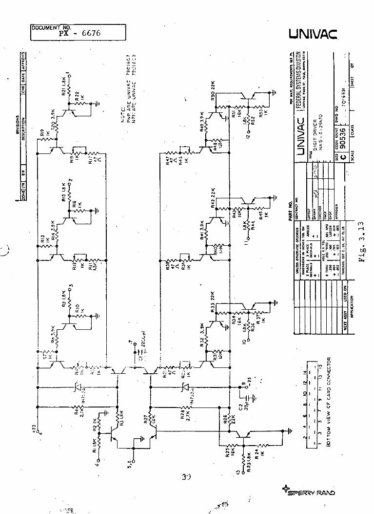
3.13 Digit Driver ~ 39
3.14 Memory Stack, Circuit Layout 40
3.15 Word Line Terminator Circuit 41
3.16 Decoder/Memory Selector Interface 42)
3.17 Sense - Digit Line Selector 8NK 43
3.18 Second Level Sense Selector 44
RAIXD

DOCUMENT NO.PX - 6676
FIGURE
3.19
3.20
3.21
3.22
3.23
3.24
3.25
4.1
4.2
4.3
4.4
4.5
4.6
4.7
4.8
4.9
4.10
4.11
4.12
4.13
4.14
4.15
UN
LIST OF ILLUSTRATIONS
TITLE
Digit Selection Board
FET Selection Line Driver
Word Line Selector Circuit
Second Level Word Selector
Sense Amplifier
Signal Envelope Detector
Comparator Card
Sense Digit Gate for MirrorMemory
Mirror Memory Word Gate Package
Stack Plan, View, Identification and Addressing
Center board Assembly
Sense/Digit Overlay Line Resistance Measurement
Word Overlay Line Resistance Measurement
Crossection of Centerboard Showing MagneticArray Construction
Sketch of The Sectioned Dummy CenterboardShowing Actual Dimensions
Magnetic Array Test Data (Before Assembly)
Digit Groups
Address Locations of Magnetic Arrays andOverlays in the Stack
Word Noise as a Function of Word .Address
Word 0111 - Down
Word 1000 - Up
WRI's - WRO's
PAGE
iLi
IVAC
PAGE
45
46
47
48
49
50
51
54
60
66
68
70
71
74
75
77
81
89
90
97
, 98
100
JL
RAND
DOCUMENT NO.
PX - 6676 UNIVACLIST OF ILLUSTRATIONS
FIGURE TITLE PAGE
4.16 WRI's - WRO's, Digit Group 001 102
4.17 All Digit Groups Except Oil & 111 103
4.18 Digit Groups 104 - 107
4.19 Folded Stack 108 - 113
4.20 Read Zero Curves 115 - 116
4.21 Folded Stack Disturb 120
RAND
DOCUMENT NO.PX-6676 UNIVAC
1.0 Introduction
The oligatomic thin film technology offers a solid
state/ fast access/ non-destructive read-out mass
memory exhibiting both low volume and low cost.
This approach is sometimes called the oligatomic
(literally "few atoms") memory because the storage
medium is only about 100 angstrom units thick and
sometimes called Mirror Memory because the storage
medium physically looks like a mirror. These terms
will be used interchangeably throughout this report.
Definition
This memory is made using the mirror technology by
forming a storage "array" consisting of a small piece2
of glass (e.g. 2" x 2" or 25.8cm ) upon which is
deposited a copper ground plane and a 100 A
continuous film of nickel-iron. Storage elements are
not discrete/ but are determined by the intersection
of orthogonal word and digit lines later placed over
the array. A large number of arrays are laminated
to a "center board" approximately a foot square,
four to six of which constitute the storage part of
the memory called a "central stack". Hybrid-word
and digit selection and sense preamplifier electron-
ics packages are mounted on similar sized "end boards."
RAfSD

DOCUMENT NO.
EX-6676 UNIVAC
The center boards and end boards are placed in
proximity to one another on a planar surface and
connected with hinges. Long word and digit line
assemblies traversing from an end board across the
centerboards (containing mirror arrays) to another
end board are laminated in place and connected to
end board electronics. A keeper is then laminated
over the word and digit lines. The resulting assembly
is folded up like a road map to give a memory stack
containing storage elements, selection electronics
and part of the sense electronics for a large number
of bits. A stack of this construction containing 10
million bits would occupy less than one-half cubic
foot.
Low Cost
There are very few parts to a mirror memory stack/ as
can be seen from the description above in addi-
tion there are no high density connections to be
made because the high density word and digit line
assemblies fan out over the end boards to low density
connection to the electronics. Univac estimates that
this memory can be made at low cost (.2 - .4C/bit).
Reading
Reading is accomplished by applying a sinusoidal
word current whose field oscillates the magnetic
RAND

DOCUMENT NO.PX-6676 UNIVAC
vector through a small angle producing a flux change
at twice the drive frequency. Phase of the output
signal depends on the orientation of the magnetic
vector with relation to the film "easy axis". Thus
a "one" or a "zero" is indicated by the phase of the
output signal. A shared reference signal is used
to allow reading by means of a differential amplifier
which compares the phase of the signal of interest to
the phase of the reference. Removal of the sinusoidal
word current leaves the magnetic vector in its initial
state/ thus defining a true non-destructive readout
memory.
Writing
Writing is accomplished by applying the same word
current as in the case of reading/ causing the same
magnetic vector oscillation while at the same time
applying a steering digit current whose field causes
the vector to creep to one or the other stable easy
axis orientation depending on the polarity of the
digit current.
History
The mirror (oligatomic) memory was conceived by
E. J. Torolc/ Univac Defense Systems Division/ Research
Department in 1967. Initial work verifying the
concept led to the operation of a few bits in 1968.
RAND

DOCUMENT NO.PX - 6676 UNIX/AC
Several years were then spent searching for a combination
of the right geometry and material composition offering
a large array of bits operating with good margins. Array
feasibility was demonstrated early in 1971. The next step
in the development cycle was to demonstrate memory
feasibility by operating arrays of storage elements spread
over large areas as would be the case in a memory stack.
This activity, funded by NASA, Huntsville, led to the
feasibility model which is the subject of this report.
Feasibility Model
The NASA mass memory feasibility model is a partially
populated version of a 10 bit mass memory (Fig. 1.1,
1.2). It contains 8000 bits located at extreme and
central areas of the stacks. These locations allow worst
case drive currents to be evaluated while avoiding the cost
of a fully populated unit. Selection electronics and
sense pre-amps were designed and fabricated in hybrid
form by thick film and beam lead chip technology. Forty-
eight inch word and digit line assemblies were fabricated
by a standard photo-lithographic etching process and the
mirrors were fabricated by thin film vacuum technology.
The feasibility model consists of an exerciser unit and
a stack unit. The exerciser contains the control panel,
power supplies and electronics for test patterns
generation, writing, reading and error detections.
RAND

DOCUMENT NO.
PX - 6676 UNIX/AC
4J•Hc
h0)V]
•1-1o
§1
60•H
RAIXD

UNIVAC
B
Csl•
i—I
00•HPn
RAIND

DOCUMENT NO.PX-6676 UNIVAC
2.0 Theory of Operation
The oligatomic memory differs from conventional
planar film memories in the following ways: (l) The
film is 100 A* thick instead of 1000 5L (2) The bit
density (15/000 bits/in2) is 100 times that of con-
ventional flat film memories (eg the Univac 1107
control memory or the S-3A solid stack memory) and
can theoretically be made greater by another factor
of 100; (3) the films are continuous mirrors instead
of discrete spots, thus eliminating registration
problems; (4) the word current is a pulsed radio
frequency alternating current instead of a dc pulse;
(5) the film signal is an rf sine wave at double the
word current frequency instead of a dc pulse; (6) the
sense amplifier is tuned to double the word current
frequency (this eliminates capacitive and inductive
word noise); (7) the memory has non-destructive
readout (NDRO); (8) the memory is "bit organized"
(a bit in the middle of an array can be written
without disturbing any of its neighbors which allows
a "square organization" with a minimum of selection
electronics); (9) low level gates are used on the
sense-digit lines so that only a few sense amplifiers
need be supplied instead of a sense amplifier per
line (this reduces cost, power and weight); (10) the
word current amplitude is only 50 mA p-p instead of
RAf\D

DOCUMENT NO.PX-6676 UNIVAC
nearly an ampere; (this means lower power, and is
within the current capability of future monolithic
integrated selection matrices); (11) switching is
by a fast form of. magnetization creep instead of
rotation (this trades switching speed for higher
margins).
The memory is constructed in 5 layers (Fig. 2.1).
The glass substrates are coated with 40,000 A* of
copper to form a ground plane. After an insulating
layer of SiO/ a 100 A layer of Permalloy is vacuum
deposited. Photo-etched overlays are attached on
top with a spun-on layer of epoxy. A metal foil
keeper is placed on top of the striplines. Hybrid
word gates are connected to the end of the word lines/
and hybrid low level sense-digit gates are connected
to the end of each sense digit line. A 10 MHz
oscillator supplies the word current. The sense
amplifier is tuned to 20 MHz and is used to read a
one bit word. The memory is made in a single plane/
and then folded like a road map into a more compact
package.
An exploded view (Fig. 2.2) of a small portion of
the memory will be used to describe the element
operation. Each intersection of a sense digit line
and a word line defines a bit location.
RAIVD

DOCUMENT NO.PX - 6676 UNIVAC
1c/i
_M
%PQ
(N
W)•H
\l

DOCUMENTNO.PX - 6676 UNIVAC
H-z:UJ
SLLJ«JLU
UJ
ccpCO
ccoUJ
CNJ
W)•H
DOCUMENT NO.PX-6676 UNIVAC
If there is a reverse domain under an intersection/
the bit is said to be a "1". If there is no reverse
domain (i.e./ if the magnetization is in the same
direction as the surrounding area) the bit is said
to be a "0".
The bit is written with a coincidence of word and
digit current: A word gate is enabled/ sending 50 mA
p-p of 10 MHz current from the oscillator down a
single word line. This by itself is not sufficient
to switch a bit. However/ at the same time a digit
gate is enabled/ sending 35 mA dc pulse down a single
sense-digit line. This also is too small to switch a
bit by itself. However/ where the two lines intersect/
the combined field is sufficient to switch the bit by
magnetization creep. The polarity of the dc digit
pulse determines whether the bit is written into the
"1" state or the "0" state.
A bit is read out by enabling a single word gate. This
causes the magnetization vector under the whole length
of the word line to rotate back and forth with a
frequency of 10 MHz. When this happens; the
component of magnetization orthogonal to the sense
line increases and decreases twice per cycle/ so the
flux around each sense-digit line changes at a 20 MHz
rate. The output of a "1" state differs in phase byr PASE '
11
"lfSPER*Y RAIXD

DOCUMENT NO.PX-6676 UNIVAC
180° from the output of a "0" state. Phase detection
is performed using a dummy line (there is one dummy
line for every 8 sense-digit lines). The low level
gate at the end of the selected sense line is enabled/
connecting the sense line to one input of a tuned
differential preamplifier. The dummy line is
connected to the other input. If both the dummy bit
and the bit to be read out are in the same state (i.e./
neither has a domain) the output of the differential
amplifier is zero. If the bit to be read is in the
domain state, its signal is opposite in sign to that
of the dummy bit resulting in an output of the
differential tuned amplifier. A peak detector con-
verts the ac output to a conventional dc logic pulse.
" RAIVD

DOCUMENT NO.PX - 6676 UNIVAC
3.0 Feasibility Model
3.1 General Description
The Film Mass Memory feasibility model consists of two
physical modules, the Exerciser Unit and the Memory
Unit. The interface between the two modules consists
of a 34 conductor cable assembly unit and 3 coaxial
cable assemblies. The 34 conductor cable assembly provides
the memory unit with addressing logic voltages and d.c.
power. The coaxial cable assemblies transmit word
and digit current (input data) to the memory unit,
and sense voltage (output data) from the memory unit.
3.2 Memory Unit
The memory unit contains the stack assembly. Also
contained within the memory unit is the sense amplifier,
integrated circuit wire wrap panel (for drive line decoders
and stack cable assembly terminations) discrete circuit
card wire wrap panel (for logic level translation cards,
second level sense selector card, and sense comparator
card) and the necessary cable assemblies.
3.2.1 Stack Assemblies
The stack assembly consists of the following
subassemblies: 4 memory centerboards, two
sense-digit selection boards, two sense-digit
termination boards, two word selection boards,
and two word termination boards. Attached to the
outside of the folded stack is the second level
RAfSD

- 6676 UNIVAC
word selector card.
a. Memory Centerboard Subassembly
Each memory centerboard has 49 locations
measuring 45 x 50 mm for magnetic storage
arrays. Each magnetic storage array is
fabricated on .178 mm thick glass substrates
by vacuum deposition processes. Each centerboard
has 2 locations which are populated with tested
magnetic storage arrays and are directly addressed
by the selection circuits.
Two other locations on each centerboard are
populated with untested magnetic storage arrays
for purposes of word current monitoring and can
be addressed only by physical wiring changes.
In addition, 15 other locations have magnetic
memory storage arrays immediately under the
electronically addressable word and digit lines
to represent a uniformity distributed transmission
line impedance. The remaining 30 locations are
populated only with glass substrates.
Each centerboard contains approximately one half
total length of the 4 digit line and 2 word line
assemblies which comprise the directly addressed line.1
Each centerboard also has 2 indirectly accessed
digit line assemblies for word current monitoring.PAGE
14
lrSPER3Y RAI\D

DOCUMENTUNIVAC
Each digit line assembly 7016709-00 consistsi
of 8 active lines, one dummy line, and one
spare line which can be used as an active or
dummy line depending on the voltage connections
made to the sense digit selector circuit.
Each word line assembly 7016708-00 consists of
two groups of 18 lines of which 32 are active
and 4 are spare lines. Activiation of the spare
lines is accomplished by, changing connections
on the enable inputs of the word line selector
circuits.
Counting only active lines, there are 64 sense
digit lines and 128 word lines directly accessible
in the complete stack. The locations of the active
lines in this partly populated stack have been
chosen so that a performance evaluation will
demonstrate that a fully populated stack is
technically feasible.
1. Sense - Digit Selection Board
There are 2 of these subassemblies in the
stack each of which consists of 4 hybrid sense-
digit selector circuits 7016688, their associated
external discrete components (including a multipin
input connector and 4 coaxial output cable
JLRAt\D

- 6676 UNIVAC
assemblies) and the printed circuit base
board assembly 7016705.
2. Sense - Digit Termination Board
There are two of these subassemblies in the
stack which consist of a ground layer printed
circuit baseboard and the digit line assembly
termination pins.
3. Word Selection Board
There are 2 of these subassemblies in the stack
each of which consists of 4 hybrid word selector
circuits 7016687, a multipin input connector,
8 twisted pair cable assemblies, and the printed
circuit base board assembly 7016706.
4. Word Termination Board
There are 2 of these subassemblies in the stack
each of which consists of 4 hybrid termination
circuits 7016689 and a ground layer printed circuit
baseboard.
b. Second Level Word Selector Boards
This subassembly mounts on the side of the frame
next to the folded stack. It consists of a hybrid
word selector 7016687, a multipin input connector,
a coaxial cable assembly, 16 twisted pair output
connectors, a two layer printed circuit assembly
7016710, and a number of discrete components. Some
rSPER3Y RAIVD

6676 UNIVAC
of these discrete components are used to
match the word current generator (located in
the exerciser) to the load representing the
second level word selector, twisted pair cable
assembly, first level word line selector, and
the word line assembly.
c. Stack Mounting Hardware
Mounting hardware is attached to each subassembly
item a 1 through a 4 inclusive as shown
in the Memory Stack Assembly Drawing, 7016665.
3.2.2 Sense Amplifier
The sense amplifier is a commercial unit manufac-
tured by RHF Electronics Laboratory Model EVT
2004 RFI Serial 5-621-1. Salient characteristics
are 90 db voltage gain at a center frequency
of 20 MHz and a bandwidth of 4 MHz.
3.2.3 Integrated Circuit Wire Wrap Assembly
This unit is manufactured by Augat, model
8136-DG. It is designated as Panel A3 and
serves three functions, 1) as a mount for the
seven MC4006 P decoder circuits required for
address decoding, 2) as a multipin socket to
terminate the five stack cable assemblies
(consisting of 14-14- pin connector plugs) 3)
as a mount for the resistors terminating the logic
signals which emanate from the exerciser unit
RAIXD

DOCUMENT NO.
PX - 6676 UNIVAC
3.3
via the 34 conductor interface cable. Circuit
and plug assignments are shown on drawing 7016703.
3.2.4 Discrete Circuit Card Wire Wrap Panel
This panel is Univac fabricated. It is designated
as Panel A4, and is used to house 14 type 7016690
translator cards (designated EXP - 6550A1) the
second level sense selector card 7016711,and a
single sense comparator card (designated ICBM-4).
All of these cards are pluggable via 15 pin male
card connectors. Card assignments are also shown
on drawing 7016703.
3.2.5 Memory Unit Chassis Assembly
This assembly 701663 consists of a metal framework
with front and back panels which houses the stack,
sense amplifier, and panels A3 and A4. This
assembly then slides into a standard comma: cial
enclosure (Optima E - 081920 D Instrument case).
Exerciser Unit
The exerciser unit consists of the exerciser control
panel, integrated circuit wire wrap panels Al and A2,
discrete circuit card panel A5, five dc power supplies
(commercial grade), rear panel (with cooling fan), and
the exerciser unit chassis assembly. Primary power
required for this unit is 60 Hz single phase 115 + 10
volts with a load capacity of at least 5 amperes.
RAI\D

DOCUMENT NO.
PX - 6676 UNIVAC
3.3.1 Control Panel
The control panel has two functional groupings
of controls. The left 1/3 of the panel consists
of the controls for: primary power, secondary
power increment, memory digit and word current
increment, and sense threshold. In addition a
meter in conjunction with two other switches monitors
these voltages and currents. The remaining two-
thirds of the panel consists of the controls and
indicators necessary to exercise the memory unit.
Because of the number and complexity of these
controls a separate checkoff list for functional
checkout is included in a separate section, 3.2
3.3.2 Integrated Circuit Wire Wrap Panels Al and A2
These two panels together are required to hold
the integrated circuits necessary to exercise the
memory unit and to permit their interconnection.
A plug strip at the rear of each panel permits
the 8 front panel interface cable assemblies to
be removed easily should maintenance be required.
The circuit locations chart, drawing 7016703, shows
the location of the 119 integrated circuits and
the 8 interface cable assemblies used in this
assembly.
•feSPER3Y RAf\D

DOCUMENT - 6676 UNIVAC
3.3.3 Discrete Circuit Card Panel A5
This panel is used to mount the digit driver
card designated (DIGIT DRIVER 8NK) and the
word driver card designated (WORD DRIVER 8NK).
Each card is pluggable via a 15 pin male connector.
The output of the word driver card is transmitted
via a coaxial connector and a coaxial cable
assembly to J9 on the rear panel. The word
driver frequency is nominally 10 MHz and is
crystal controlled. Power capability of the
word driver output stage permits an output current
of 35 ma rms in a 400 ohm resistive load. Digit
driver current capability is + 75 ma dc. in a
100 ohm resistive load. The output current
on each card can be incremented or decremented
separately a predetermined amount by means of
front panel controls.
3.3.4 Power Supplies
Five dc power supplies are used to power the
exerciser and memory. The list below gives
the nominal supply voltage, vendor name and
model, and whether the voltage can be incremented
via the front panel switch.
•feSPERRY RAND

DOCU-EN).J.Jf).,
UNIVAC
VOLTAGE
+5
-5
+25
-25
+100
VENDOR
LAMBDA
LAMBDA
LAMBDA
LAMBDA
TEC LITE
MODEL NO
LXS-B-5
LCS-B-01
LCS-B-03
LCS-B-03
LPS-102
3.3.5
3.3.6
INCREMENTED
No
Yes
Yes
Yes
No
The purpose of incrementing or decrementing
the voltage supplies is to demonstrate the
functional reliability of the memory circuits
(line selectors, logic translators, current
drivers, sense preamplifiers and sense amplifier)
The exerciser logic supply is not altered sirnce
the reliability of these commercially available
circuits is well known.
Rear Panel
The rear panel serves to mount the following
components: cooling fan, power receptacle,
fuse holder, memory interface connector J12,
word current output jack J9 digit current output
jack J10, exhaust air louvers, and test point
jack J13.
Exerciser Unit Chassis Assembly
This assembly consists of the framework to which
items described in Sections 3.3.1 through 3.3.5
JL.RA1ND

UNIVAC
inclusive are attached, according to
drawing 7016662. This complete assembly
slides into an Optima model E-081920 HD
Instrument Case enclosure. A necessary part
of this assembly are the power cord and interface
cable assemblies: 1 multiconductor and 3 BNC
(male connector ends).
JL~ RA(\D

DOCUMENT NO.
PX-6676 UNIVAC
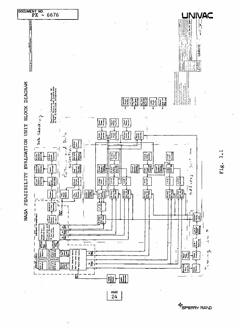
3.4 Block Diagram
The NASA Feasibility Evaluation Unit Block Diagram (Fig. 3.1)
consists of a memory assembly, memory array/ address
selection circuitry, pattern and data selection
circuitry, data checking circuitry, and a timing
section.
The memory assembly contains the selection circuitry
for accessing the memory array. The word selection
matrix system has 128 first level gates and 16 second
level gates. These gates distribute the 10 MHz word
current to the 128 word lines. The sense-digit
selection matrix system has 64 low level gates, ,
8 sense preamps with gates and 8 high level digit
gates. The 64 low level gates are common to both
writing and reading functions.
The memory array section is assembled from 4 center
boards. The center boards are only partially popu-
lated. The 2048 bits on each board are accessed by
64 word lines and 32 sense-digit lines. The combined
memory array section is represented by 128 word lines
and 64 sense-digit lines.
The address selection circuitry consists of FET drivers
that selectively enable 24 word gates, 8 sense-digit
gates. These FET drivers are selected by 6 decoders
RAND
DOCUMENT NO.PX - 6676
IT
BL
OC
K
DIA
GE
VA
LU
AT
ION
SIB
ILI
56
NVAC
a it
i - y i 1
!iU-i
;y3
g F-=
F
J
c
\C-
!1j\
r '
x
t*l<
j
|
51\£
|_
•£K
J
*
»
i!?}
*[
- -
a
1
Isp]ji
i -f
f ?
„
-
-
. —
M:i
JJfl|
I*1;i2o2
Mf£«J
I
* s.*i»iill!I
ii-t--1-1w, .»ii^?' c
ij J
•*1* i
f *
r -l-
5?
i
""*'
Ci
i *«! *
: x "
;. ^'T^
0\Y»
r~
' III,
! _ . . __ ,
-.*of
' -li• A * 1
•J!
~
&!!£
<^
i;%
o
'
i
lit0* t f )
1in:111=
1
JillI1
HiJ 1
-i
! I JMi ?5 '
u
f
i'fll-I ^ 0 J "
1
n
•i!'
j»!XiT
J
U!i? = /
^13•
2|Jj
|!li
111
iiMl• if
}
M,I
* * ^
« fa j
i-5?ls
1i• X• 1-S
J*~~>
"• • '"»
th*|J
i> 1
(i
\$
_
f•
IIi
S 5Ji
"A1
i 5U
ii
1j
j
5 j
«J
f
?JJj
|f
||
/J
1
1
|ij1
*\i\iia $
1
!!!
ii]pi
'111 j*iij
ii iiinii!JV
j
.
li*til
1 .i1-3
(^
V".
SJ
^
1
If1
?]
i ,lij
;i£ '1
«*
i
i[
\i
•
^
ro
W)
PAGE
24
RAIMD

DOCUMENT NO.
PX-6676 UNIX/AC
which are operating off the address counters.
The pattern and data selection circuitry consists of
the digit driver/ bipolar generator/ address and data
mode controls/ and automatic pattern control. These
circuits allow manual or automatic data and pattern/
writing and reading of the memory array.
The data checking circuitry consists of a video
detector/ a strobed comparator/ data register/ data
compare/ and error counter. A narrow pulse is used to
strobe the comparator to sample signal amplitude during
an interval of minimum noise. The data is then at a
logic level and is stored in the data register. The
indicator lights give a visual result on each bit or
a total can be read off the error counter.
The timing section provides 8 timing pulses of equal
intervals. These intervals are distributed thru the
system to enable the proper sequence.
RAI\D

DOCUMENT NO.PX - 6676 UNIVAC
3.5 Circuit Diagrams
Included in this section are all the diagrams with
the exception of those for commercial purchased power
supplies. No attempt will be made to describe each
of these circuits; however, there is a discussion of
the hybrid circuits made at Univac in Section 4.2.
o Switches and Indicator Lights
° Power Distribution
,o Circuit Location Chart
° Clock, Divider, Phase Counter and Decoder
0 Word Address Counter
o High Digit Address Counter
0 Sense-Digit Address Counter
0 Decoders
° Digit Driver and Input Register
0 Output Register and Error Compare
° Word Driver 8NK
o Digit Driver
o Memory Stack Circuit Layout
o Word Line Terminator Circuit
o Decoder/Memory Selector Interface
o Sense-Digit Line Selector 8NK
o Second Level Sense Selector
o Digit Selection Board
0 FET Selection Line Driver0 Word Line Selector Circuit
L'AGE
2A
RAI\D

DOCUMENT NO.
PX - 6676 UNIX/AC
o
o
Second Level Word Selector
Sense Amplifier
Signal Envelope Detector
Comparator Card
"feSPER3Y RAISD

DOCUMENT NO.
PX - 6G76 UNIVAC
FT
9 (53 3
©
4 « «
a. 8
gig
©
© © © © ( § ) ©
I® <i® 4© ©3© © © © © © ©
«N•
ro
PAGE
23
"SPER3Y RAND

DOCUMENT NO.
PX - 6676 UNIVAC
-So
•Hud
S •
:tr
2OHH
§
HP
o$
04
«:.-
-So
UU
D •
a * 51 ]-oJ i ° °7:w/*nv» ,j __=-J-_^-) I
—T- 0« S.j-'O-'L'
' 1 g-V-rt.AlddOS M16 X*3W/1 »W.
< _0» «!'(s«-ie «*)i'*«ie w
G^nqs-tj^r A> B
1
ri
1 1_i!
• '1-u.1 11 L
1
iI
i j1I
5 i
| sill• I '
1 (SS
11
tJ-J* ,'l
1 *\
. V §?r- 1 *f ?'
1 3V** DO
1
111
-OX
- OO I*** " -"*
- f "3
6 6 0 3 O Sr*
r l«~h—ii _. i ; t L^.___ l
29
•fe
W)
SPER^V RAIXD

DOCUMENT NO.PX - 6676 UNIVAC
["*'»•]
-CE3
-E3 EE3 EJ EE3 EE
EE3E3E3fc(.~H;Frq;|-HiF"^l
^F^ EJ3 EE3 F-*! EEE1153
II
EI3 EZ3 E3 E3 EE1
-CDHOEE•fin
•cncricx]
'E31E3
If
5*
V1
jsj
% os» °
Kj^-
Ufi
55
mjrtrHr—n i «sa-g» i| • I
ro
U)
RA(\D

DOCUMENT NO.PX - 667G UNIVAC
n
00•H
31 "SPERRY RAIVD

DOCUMENT NO.
PX - 66 7 6 UNIVAC
LrS.jNv. y*
00•H
RA/\D

DOCUMENT NO.PX - 6676 UNIVAC
•K t>-«»
Ml CH-<T
?«-J
K~;
! '
1
*
-
*
T
-
*»
I
1
k
IiN*— i
r(-
=T^T-
H
_4"7~. k.a
. .v^
f
K
ro
00-rH
RAfVD

DOCUMENT NO.
PX - 6676 UNIVAC
CD•
ro
U)•Hb-.
34RAIVD

DOCUMENT NO.PX - 6676 UNIVAC
s!
i-IE
1!
lis
1Cuwx 1 1
o"nTi"ni(i
1±~
CTi
CO
00•r-l
35RAND

DOCUMENT NO.
PX - 6676 UNIVAC
iPfijf.ii
i6
II
b >
I!li0!<
?!313i
1
IT
1(J
u' u
:;»
!
f:
1 !iB|i*-!
= 1
i!
LI
5
i
y>1 r
00°
* S
2
e..-1;
lysis
Nil
_
-
-
-
-1
"r
i22
o-H
»ro
W)
^T • ~"T2 ''s "if" '•"» •:! i«5 ~i.1 1 i 1 II 1 i I
36RA(\D

DOCUMENT NO.
UNIVAC
rH'•H
•ro
37 SFEF7?V RAND

DOCUMENT NO.PX - 6676 UNIVAC
S
H,,'
5
§-
IiKil5 &
£§
2 e
OCO
§FoCOz:buC
rV
<NX
!i3
1-
fafe 3
"
ilDiu
1
[LA
YO
UT
1ERW
ISE
SPEC
IFIE
D
'
HiO
SS
3W
9
24
:V
•aC
IN I
NC
HE
S T
OL.
ON
iP
LA
CE
A
NG
LE
SP
EN
SIO
NS
PLA
CE
3
-
z*" jjcr ivUUJ> c^
Q^ 'Q <"
n 'tr tf)
*z
3
^
•
11-h I
3
o.t I
3
a*"* S + t
0
s!
1
• — "
(Tt'D
6 2z o
f "0 . .
1 w
9 U)o .O3i°»so
|S2< O o_ tt '3 < -»-rj --
3§«n
O
^
p.§sO "*"
m
t
U
X
Q
ui
X
Soo
10O
og•1-1
DO
lfSPER^V RAtVD
DOCUMENT NO.PX - 6676 UNIVAC
o
<
t3|||£s3
i
O ;CO ".
o I§ <
•^ ss:tj^j ^it j 3;tr §
y °<( 2
> ?
Z c.3 |e
at
y
i
§ ifo
ibf
5
|
SI
5 3S " 4
w
5 »3%'S
*"»•»
III
OK.
J "
li
\
<-i
0
g 0 .
s s s0 M M
(7ku>u>
6i "oo
ISo OSen
so
o
AP
PfiO
V
Isss .< u o 5 «
. ' z
03 ^
o • • "- <J
g3 + a= o«~ S|~88 s0 + I "
ICu«
1
Ci
o
^_
5.
_
O
51
i
nH
n
W)•rj
iI i
5
or; P
ii
iI
i
ii
i|
Ii
ii
i
^ ou
•0 z
az o
<n •->u.O
5Ul
<n 5
5o O
\—
- a
'SPERRY

DOCUMENT NO.PX - 6676 UNIVAC
I 0-0
rvi • O
fM I O
a)1/1
-U) ui 5 „ u:)- i/> $ S inDo ^ T> W
y — - - 0 0 8 8— OJ O -J
Ld«
a-
^G
CD
°4U
_J Z -SZ92d
J >-»««-
Z-919/ d|
. .
ni
(DinQ
1K.
Q.
m
$2 o<a o
iyi
iD
mu).o
-g
* dliiiilLlllilili.21r- I •» a
l ___ J
tf
ou
8
a
*•
*Kv>3|«=2^j
!!
i
CO •
S !to '
£ ^S !^! •f"i *"^ uti^ >UJ Jd 5
U!
5S!!1i
• i' Jj;
ata
3O
5
_
f}
a:
So
UJ <]5 Z
3
|
**,'K
^X
|6SoS
«* +
iBlZfc ?
5 O "*"
9-22°3
l«g +
1
1
«
2iUJ
° « Oz u, „.< O o
0 ^ +
Jlgll5— " '«*^
3 e« f|S§J0 +
"'1
:l^
j
'ON
OM
al
:ODE
IOEN
IJO
.
S0536
so
<jk
n £
|••s- u
K.'
X
ijX
i*.Q
t
1
C
uC
i
UJ
O)u-
i
s
)
00-H
'SPER^Y RAISD

lOOCUMENT NO.
PX - 6676 UNIVAC
rg « -•M O • <
cv O *
«n - .
to „ 4
m -cv °
0 o
** 0
« o |
n ^ *
• O i
" o-- i
oV O *
)"
or
£
I.B
tt
o:
tr
tr
1 .2.a*
tt*
Oa
mor
er
a:
(0a:
a:
a.
a.
fMcc
i ->/VA/<
O °
O **
O lO
— . n -
S
aia
c
pIiIIR *
MA
nK
<IE
VLE
TT
5!
rmo m
*.B
EN
TNO
.
cV
1t/
•3u.
£t/$Z
tru_C
C<s
*••V
m
|tuI
-5
5
sit.
OSs1tuX
I
UN
LES
S C
» rt ••t •- t
i !
1 4
* J
1 *> 1
5:a
ji£i1 3
_ r1 r
';ii
zwsthZ BL
i D
IME
NS
ION
1 I
PLA
CE
•J
d'
O
(t "O
4
IIu
w/^
_Jn
>
UJ
/
t
C ' > Of
^' S S;:~i S 2f - B 05 5 5
° « c<Oc
5< H
1 ?ilig*,|s^
1 1^J| + i » H
6
io
ztuO
ituIM
>s0-
> <o>0
" 1
> o)0
h 1
oi O
- 1
-w
1
oin
^o
O
c«
U
|
= 8tu i—
1 T
HR
EA
DS
:
ICO
MM
ODI
41
IT)r-H
•ro
00
RA/\D

DOCUMENT NO.
PX - 6676 UNIVAC
1
3 3 3 3 ? g 9 S 5 S
,$11S.?f "*i51J!
O S
Ii
||S'
1!SiS |
o;
2!2153
55eo-Ssir ;«III" If" "
$:1*'
ito
u
,.orO
iC
0
C_J
Ll
I
I"
fa »rB *
Ul
a:ij
£
s;
t•~
•
iI?Si!«ocS3-
Ilips*
•n -v»
I
«•or-S
? 6? ^d -
lo°
I1.{
jl
_J -
1' • "
..-I
I-
:-
•\2
\33i8
W)•H
P^AfVD

^—oo
UNIVAC
4
CO «
S i
IJSH«S + I
6 •&
O t~I
^ g s sg>-*. 99
«i
O "O U) ^
O1^ rTVT*0"oj O fty (^ ^- <NJr> Kl (M f\j C\i (\j
. T — <Ti f1* uT *••) —rl Kl C\J fv CXJ ^ O*
1i
i1
T ""
43
' 9" * T '.O X> O— — — ^1
RAI\D

DOCUMENT-NO. ,..-r- DO/0 UN
5.Ul
1 v>
z «< zZ £o S
Q£
" Ct ec
< <- (\ Z
o 5 2 su. o 2<~» Z 0-• < csj
or _' Q<0 Ct*-*
0Z
«
*"^ ~c/i ".
?5
S|.
S?S5<o >u- ?
^Z-3
1
ur-CJ(ll
<N (\Jre 'O •';'^~ (/)
UJ <
Idin
"jLJ r .
<£ w^ <I/is
llO —
^ ^O
^J ljj
tu ^
° r\
3
s 2 i° < tu
5 o <->
goSE -*o
I?1 +'S SlU J_ Vjj ^
|-5*
I ««^+ 1° OjuS
S ^5s= I«B-H
tuIUzoztu
VAC
-*.
-u>o .rt
i
?0
1mgou
- CQ
oa.
^°«0*> S
<Oop y
.§541 z
J-COOO "
*z"'+\ "2 1U
=,or>n g
|S§§ go -MX
5
tMl
X
••—
—
UJ
<
oI->-oCD
a:oh-uUJ
' ouoto cro
CD
00
00
"SPER^Y RAIMD

DOCUMENT NO.PX - 6676 UNIVAC
S H
—jqif~7^
t
j. 3"' Iti «
-t
3( . --B
|H^?: s l id- ^- 858?
9
« C>-. . . .--:•-••:•c«« -
J
> «RZiIt |-v) 4 |l
§ *"*» «- - .-
gr^
H^ Fni- J?
ff"LJ
^n
11
S
IIfsF u
SiH
§ii s
1
S|l!B'
1}
5i
I?!21\i
f1 -s S
o
,"*,
jj* *j
'"•i0 2.
|
"
. 2• S
S5 oi= 5«r?» .,"t -s —
Hi!Cp*pl»I-8*.
2?
|
|"< 3ps3«!,!M" —«*K|-iA• *
_
8 I
c .,. I-'.p - _
«_* —
r -* . . * ' -S o ? JS !; Ki«s3 sV-
I!
E ;
w
'!- <•8;
1
s3
j
3
|
s
| '* {- "°tlT^fepF- v-fi ?s
o - o - o - o -
cr>
ro
00
45
RAND

"""fir*: 6676 UNIVAC
1
11
11
11
11
11
o~ 3
O•> ^-
V-0
- fO(
crtfi o
t-f i
»-- iu
n 0u
K> Orr
- O
Ja
oa
iOa
u
~
<:;:i •_
Co
Co
GO
LJ
0z.
uf
C0
Co
o
Iton
u
_.— 1
1J, — — .
*>
tlJ Q
3 o
l/l
tfloor O ,
ooI
.
's1ao2J
P
a|
it2
ar Sep S£o «*S?0 j
s=fSjJi— .y^ sCO *
s;£7j *i
o stt!i
UN
IVA
C
i1 I3 *
bs§s3M
U3IU
O
ten
§
crLI>
troLJ
5_J
- o2 ^1- U)O <MLJ ir! w10 I
>• -2L.I •»Lu Z
1
|
?a
_ u
ISg s
§ 5^ 5 J. It- T 1
&
Ss3;2S
^S+,IJT** S+l
5 S5 5
r(7
O •;
~
i r~0
zUDSCOI""
R C3
au1i
iilissi + l "• S
3= ~""RES S
o w- 2
*zǤi ae +1 S
iC
S
KX
O
v-UJI
™—
5
5
1
*
oCM
•H
VA
C
79
01
79
00
IO6
E IVO
RS
R£
RAND

DOCUMENT NO.PX - 6676 UNIX/AC
ro
W)
%PER^V RAND

DOCUMENT NO.
PX - fi67f> VAC
(/)z
u<*SKz
*
t/)
Hi<-U>
oE c.cc>-»-^ToT^-> -/V>-r • *
3 S2>4-— W.v ' J
6C,3>f-
3H>rtlEizr
Tvwlrii?-^ io7x-— »W •*
<r> i £ j —o: T«ttjj2^f~
""^ i i->f-^Jji3"^ jLlli?""
^> \4-jf-
~* 6 |5<4~_^J_22*~
^ 9 7oy-LvW-4 — ' — '
— i> t*0 —1
Xto
O
1 A_
2'/.'_~ ^
£•/••—
£ •/'/_7 //_
- / /_
5 ••'•' -
1C G1 Vrf- >J
1 I -V-12-V,1 3 -'i -14 /._15 "_1 5 •'•'-1 7 -'•/-1 ; <V-1 3 •>/_
2C G
c3OOBO IB02B03B.D490S606BO 7BOd
9103 • 13 12•B 13 •314BISBISBI7BI3
• WSP_BOOSO 1802BO3804BC5ace807Boe
WGR OO• WGR 10
we R BIOBll81?BI3BMBI5
Jo BISS " B i r0 BISr**-
SELECTSELECTSELECTSELECTSELECTSELECTSELECTSELECTSELECTINPUTIHPUTSELECTSELE'CTS'ELECT5ELECTSELECTSELECTSELECTSELECTSELECr
403336573?35343332^ i•J 1
3C232-5272S252423222 1
toCCI
ft43
<NCN
W)

UNIVACDOCUMENT NO.
PX - 6676
rocxj
.bO

DOCUMENT NO.PX - 6676
I •40
£uI/!
(ft1-Z
aa
sg1
0
i
.
UNS ;to2i=
2
S2«/:
iu.°*
if
j-
S
si
Ucc>Z3
\u
I
gs
fo
6j,.LU1-
n
a'So
-^ (n<£• OJUJ i
—7
gl/1 ^
_
IU
5
S o£= g; £
S 0| 2', 2
»
Js<^
|5"g+l
i!<I3 I«s+ i
ziUl
mN-
0
oo
I
§<o? rooinj.0§w
"MR
51
§«2ss^g^o u
_. si^ 1 i?£„„„ <^ IOOO J
5^ ° '-'gS 41 5?=00., g
•cmoo <3jr«oq <
0 +1 X
VAC
£
fc.u
5"™
bi
CNI
00
RAI\D

DOCUMENT NO.
PX - 6676
zQ2 cj
D OO
•°
OZ «>0
,0
QCOp
0 OU Q.1- 1-
I
1
1
1
1
1
ii
1
1
I
1
1
|
111
i_*
~ e>«
>O fyfO
•"*
- ' •*
0
(3
K.
Q10 o'
U;^ rv-^
O_ z
13Ul DQ 0
«
OJ ""> ' u.>
T ^~
ro
f\)
e — n0 .0 >- ?-.o ^j-L
^>~ &T^^ w^j
©0 ^ ^
4
_ i
-hk^J^N-rh- !* ^>-|
© o . b>
u^)
T~
^MI-<o
0 ~
^fHi-
<
^c: h?
0^^y O
<r
o <S' "*" ft\J
HM"GOCD
QrOo
4! MI^>°gQ
5,<_Joa:o>-oin
5!
U
«
ZiU
UJ(C
o-u
1e
i'f»
A.
iC5:
E iGO
111,
1
j_js*
_J
5_A/
s„-
:w4
J
i
iiZD
3i
5e1IU
Of
*o
2Z3
zo
ajzv>
Q
$
£J
0
V-T-
CDi.
-.ntc
o ofs.
O (A)t- (M"3 i
^ U)
U*--
UJ
r.
r.< ¥0 U
w
i +lB2
^0°0+ 1
•u!3y<^ n"S+ 1
i1Ul
r
[DW
G N
O
•ro
_•\v^
|u)80
«M
Ia.
o<Ooo
jSS+i°20«no ,. ' ' .'SS ' '2
KMOP
Xr>o5
o *f 1
A«**
\i«X
i/iO<hu
XH-
o
tz
^^
-x
UNIVAC
inCNJ•
ro
00

DOCUMENT NO.PX - 6676 UNIVAC
4.0 Evaluation
4.1 Introduction
This evaluation covers the functi onal operation of
the special hybrid circuits developed by Univac
for this application and the functional operation
of the stack. The sections on Stack Description
(Sec. 4.3) and Evaluation Method (Sec. 4.4) establishes
the baseline for the Functional Stack Operation
(Sec. 4.5) discussion. While there are conclusions
drawn throughout Section 4, the summary of the conclusion
for the total feasibility model is presented in
Section 5.
RAND

DOCUMENT NO.
PX - 6676 UNIVAC
4.2 Hybrid Circuit
4.2.1 Electrical Function
There were three hybrid circuits which were de-
veloped for this contract from the discrete circuit
breadboard stage. All performed as expected,
a. Sense Digit Line Selector - The first of these
the sense digit line selector Fig. 4,1 (same as
3.17 ) selects 1 of 8 active digit lines connected
to the active input terminals. (Pins 1,3,5,7,9,11,
15) Each input terminal (pins 1,3,5,7,9,11,13,15,
17 and 19) is connected to source terminal of an
2N4856 (N channel JFET) and terminated with a 60
resistor to ground (pins 2,4,6,8,10,13,14,16,18, and
20). Eight of the JFET's serve as low level gates
for sense signal and high level gates for digit
current. The gate terminals of each of these FETs
(1-8) are connected to a resistive AND circuit one
terminal of which goes to the first level select
pins (32-39) and the other goes to the common group
select pin (40).
The drain terminals of each of these FETs are wire
OR ed together and connected to the emitter of a
2N2222 NPN transistor through an ac coupling capacitor.
The active drain bus is connected to outside world
via pin 25 and also to the source of another JFET
(9) serving as a second level digit gate. The gate
^f RAND

A.'wL
> O •-
2 0--
3 O-
4 O—
/r o—'
8 o-
o ,-\.— —•«—/ v^"" •'
O ? •'—<>
L I_ R)(
i />y\
y • A^y^^^ .[___._
~r
—-o 4-0
*S^s-
j
^/Vv-
3?
O 3d
R 1 o/Wv-
l> O~
i'b o-
/4 Q-
.s, fe" t-A/v'v
I C^ •>
j: w\—
^/W-
i! ?:v!
—*O L
17 -.It.—
<vvv
.'•.-JL-
ri .iKl' ~i
—«VV\-
54
Fig. 4.1
W/-X33
..d*
L. /^/v^v- —
HL
•RS'f
— O 2-"S
r. .'J ^ ^<VSA./W>—i 'I .t.i>
[r 1 1
-O 2<?
-O 22
-- O 2S
• 'J ri I

DOCUMENT NO.PX - 6676 UNIVAC
terminal of this last FET is connected to a resistive
AND circuit, one terminal of which is connected to
the hybrid chip or group select (pin 40) and the
other to the digit write select (pin 31).
A single JFET (11) serves as a low level gate for
the dummy sense signal (pin 17) and as a high level
gate for dummy digit current during the initialization
procedure. The drain of this FET is connected to
pin 24, the source of the second level dummy digit
gate (10) and to the base of the 2N2222 through an
ac coupling capacitor. The gate terminal of the
second level dummy digit FET (10) is connected to
a resistive and one terminal of which is connected
to the group select (pin 40) and the other of which
goes to pin 29. The gate terminal of the first
level dummy FET is connected only to pin 40 through
a resistor.
A single JFET (12) is a spare device. The drain is
brought out to pin 22 and the gate connected to the
group select pin 40, and to pin 28 through a resistor.
The spare can be used to replace either a defective
first level active gate (1-8) or the dummy gate (11)
by appropriate external wiring.
The collector of the 2N2222 transistor is brought
out to pin 27. External discrete components,
•feSPERRV RAI\D

DOCUMENTNO.PA - 6676 UNIVAC
(•which includes a parallel tuned transformer)
provide the transistor with the proper collector
voltage and couples the sense signal (which is
the difference between the base and emitter
voltages) to the second level of sense selection.
The emitter is connected to pin 26 through a
resistor to limit the transistor collector current.
Pins 23 is an isolated ground for the transistor
stage and pin 21 is an extension of the input
grounds. The drain of second level active digit
(9) and dummy digit (11) FETs are connected together
at pin 30 which is the common digit bus input.
Voltages for the gate terminals of the FETs are
0 volts when selected and -25 volts when unselected.
The large gate resistors (20K) are used to maintain
the gate voltage near the source and drain voltages
which linearizes the transfer curve and reduces the
generation of second harmonics. The transistor
stage is designed to operate at a collector voltage
+5 volts and an emitter voltage of -5 volts. The
active and dummy drain buses are brought out
to pins 25 and 24 to enable the spare to serve
as either a dummy or active gate and also to
permit external balancing of the sense preamplifier
(2N2222) inputs.
rSPER3Y RAIXD

DOCUMENT NO.PX - 6676 UNIVAC
To select any function on the chip (or in the group),
the group select pin 40 must be high (zero volts).
To select a digit-sense line, one pin of (32-39)
must be high. When reading pins 29 and 31 must be
low (-25 volts). When writing an active line,
pin 31 must be high and pin 29 must be low. During
the initialization procedure (when writing the
dummy) pin 29 must be high and pin 31 low.
There is a maximum digit current of 45 ma which can
be applied to the digit bus, pin 30. Larger values
than this require a large enough drain to source
voltage which will tend to reduce or increase the
drain to source resistance depending on the current
polarity. The end result is non-uniformity of
digit currents throughout the memory array. The
digit current uniformity was writhin + 107o in the
feasibility model.
The differential amplification of the WZ7Z2 works
for low level (microvolt) signals of either polarity.
As the signal level increases to the millivolt level,
one polarity will be distorted due to diode action
of the base emitter junction. This is not a problem
in the feasibility model.
A single chip of this type is used as the second
irSPER3Y RAND

DOCUMENTif7- 6676 UNIVAC
chip to reduce the second harmonic distortion,
c. Word Line Termination - This chip consists
of 18 terminating resistors - 8xw+ 1070. The
input terminals are arranged to exactly match
the word-selector chip. The terminals on the
opposite side of the chip are all connected to the
internal ground levels.
4.2.2 Mechanical Characteristics
a. General - All three hybrid circuits utilized a
standard lead frame having a configuration of 20
pins (on 50 mil centers) on either side of the
1 x 1.25 package.
b. Fabrication
1. Screen Printing
(850°C) on 2 x 2 x .025 inch 96% alumia substrate
1st screen- Termination Pads: 165 mesh screen,DP-8553Platinum/Gold
2nd screen- 1st metal: 325 mesh screen, AlloysC-5011 Gold
3rd screen- Birox Resistors: 250 mesh screen
Word Gate - 10 ohms per square Birox
Sense Digit - 10K ohms per square Birox
-100K ohms per square Birox
2. Ring Frame Attachment
-1.0 x 1.0 Cermaic Ring Frame (.880x.880x.060cavity)
-Ring Frame attached by screening ESL 4009
irSPERRY RAI\D

DOCUMENT NO.
PX - 6676 UNIVAC
level of sense selection.
b. Word Line Selector - The word line selector
consists of two arrays of 9, 2N4856 JFETs as shown
in Fig. 4.2 (same as 3.21 ). Each of the
9 FETs have an input pin connected to its source.
Each gate is connected to a separate select pin
through a 5K resistor,, All 9 drains are connected
together and brought out to pins 30 or 31, the word
current input terminals.
When a FET is selected the gate voltage must be
high (zero volts) and the 10.3 MHz word voltage
present at the appropriate input 30 or 31. All
unselected lines are at -25 volts. The selected
FET is in a low resistance state permitting bipolar
current flow. At current levels higher than 65 ma
(p-p) waveform distortion appears (due to modulation
of the on resistance). Currents in the feasibility
model are below 60 ma (p-p).
One FET of each group of 9 is used as a spare device
in the feasibility model. Only eight of these chips
are required as first level gates for the 128 active
lines. A single chip serves as a 1 of 16 line second
level selector in the feasibility model. A single
parallel turned 20.6 MHz trap is used between the
word driver and the second level word line selectorPAGE
59
irSPER*Y RAIVD

M.i. FY;TS aw.; 2.5V
I CJ i• ••IwfJ
"E' -nir
6
7
6 o~
9C-
JOG - : fT"-. •>. •-
16
)&'
l<* C-
--^vw
R3-^VSAr-
-O
I
•o
RS*V\Ar -O36
-AA/V— -05
R7-VS r
^VW—
L_._^/Vv—
4 .' " " " ' "**— - •
'-" .-9- 1
-v--J~,-J-
1 K r*». . . -™. i150 , ,«,r, v
" t
Rio
R\\
2
> . ; ''
O r> -i
i- 7
. , n ^7
-^/SA^- -0^.5
-'Wv-
11 -»>
-V^-v/7
'v-W-
O 2.
60Fig. 4.2

DOCUMENT NO.
PX - 6676 UNIVACsolder glass to base substrate and on ring
frame using 165-200 mesh screen.
-Preglaze 3% min. @ 450°C.
-Seal ring to cover - Weight with 50 gms and
fire for 20 minutes at 475°C. This causes
approximately 4% decrease in 10K ohms resistor
paste and 2% decrease in 100 ohm resistor paste
values. Gold bonding areas are burnished with
a fiberglass typewriter eraser prior to and
after glass sealing.
Device Bonding
Devices are bonded by applying a small amount
of Alloys Unlimited T-2003 conductive gold
epoxy to bonding pads. (Approx. .010 in dia-
meter drop of paste applied with a .005 inch
wire in a pin vise). Capacitors are bonded in
similar manner by applying gold paste to both
substrate terminations. After placing devices
in proper location, the assembly is heated at
250°C for 1 hour. In the case of the sense-
digit circuit the beam lead transistor is
thermo compression bonded prior to other devices
since substrate temperature required is 325 C.
Wire Bonding
FET devices and capacitors are bonded using a
Kulike and Soffa 472 ultrasonic gold wire
ball bonder.PAGE
61
RA(\D

DOCUMENT NO.PX - 6676
5.
6.
Approximate settings are:
Power Time
1st bond 5.50 low 6
2nd bond 4.50 low 4
UNIVAC
Force
45 gms
105 gms
Bond pull test with .001 inch diameter gold
wire (3-57o elongation) produce typical force
levels of 5-6 gms.
Electrical Test
Lead Attachment
Substrate termination bonding pads (Platinum/
Gold) are dip soldered in a solder pot contain-
ing 10/90 Tin/Lead solder at 610-620°F. Alpha
711-35 flux is used to precoat pads prior to
dip soldering. Care should be taken to prevent
flux or solder from contacting the interior of
the package. The leads are etched beryllium
copper (.006 inch thick) which have been plated
with 100 microinches of nickel and 70 micro-
inches of gold. The leads are solder dipped
on the end 3/16 inch of the lead frame. Sub-
strates and leads are cleaned with Dupont 8529
flux remover followed by cleaning in TP-35
freon and TF freon.
The Platinum/Gold termination pads which have
been pretlnned are coated with a thin layer of
711-35 flux and the tinned lead frames positioned
and aligned to the substrate. The complete assembly62
lfSPER^Y RAIXD

. 6676 UNIVAC
is placed on a 3 x 3% inch ceramic substrate
with 1 x 1 x .025 ceramic substrates placed
under lead frames to position them at the
proper height. The entire assembly is placed
on a hot plate (650°C) and heated until solder
reflows, then removed. Flux is removed and
parts cleaned in a manner similar to the post
tinning procedure. Complete removal of flux
is essential prior to the final sealing operation.
Shorting buss is cut from lead frames at this
time.
7. Electrical Test and Precap Visual
8. Sealing
Units are baked at 130°C for 2-4 hours in a
vacuum oven prior to sealing. Sealing is
accomplished using a 1.0 x 1.0 x .025 inch alumina
substrate and a perform made from Duroseal fa-
stage fiberfilled epoxy, .007 inch thick.
This frame-type perform has outside dimensions
of 1.0 x 1.0 and inside dimensions of .800
x .800 inches.
The ceramic substrate which is used for a cover
is screened with appropriate markings prior to
sealing. Material used is Wbrnowink series
M marking ink (Mixed 12 parts resin, 1 part
catalys by weight). Curing is accomplished
•feSPER3Y RAfSD

DOCUMENT NO.
PX - 6676 UNIX/AC
9.
at 125-150°F for one hour.
The epoxy perform is attached to the cover
by placing a drop of solvent (acetone or MEK)
on the corners of the preform, positioning the
preform on the underside of the cover and curing
at 190°F in a circulating air oven for 20
minutes. The cover with attached preform is
aligned over the package ring frame and clamped
in place using a bulldog paper clamp. The
assembly is heated at 250°F for ten minutes and
temperature is increased and the assembly cured
for a minimum of 20 minutes at 350°F. The
assembly is removed from the oven and cooled
prior to removing clamping force. A bead of
Eccocoat C26 is placed over the solder joints,
where lead frames are attached, and cured per
vendor recommendations.
Final Electrical
All previous electrical tests prior to sealing
are performed in a similar manner to the following
brief outline:
1. Measure source-drain resistance at 50 ma
current. This should be less than 25 ohms.
2. Measure turn-off threshold across gate-drain
junction with proper bias applied. Thisshould measure 9 volts or less.
64
rSPER^V RAIXD

DOCUMENT NO.
PX - 6676 UNIVAC
4.3 Stack Description
a. Major Assemblies
The stack consists of the following major
components: 4 memory center boards, two digit
selection boards (DSB-1, and DSB-4) with hybrid
circuits, two digit termination boards DSB-2 and
DSB-3). where the digit overlays are connected
to ground, two word selection boards (WSB-1 and
WSB-2) with hybrid circuits, and two termination
boards (TB-1 and TB-2) with hybrid terminating
resistors.
A plan view of stack is shown in Fig. 4.3 with
the substrate identification numbers and drive
line addresses.
b. Centerboard Assembly
The centerboard assembly consists of the following
major components 1) 4 base boards 2) 8 functional
magnetic arrays 3) 4 word line overlays 4) 8
addressable digit line overlays 5) 4 non-
addressable digit line overlays 6) 68 non-functional
magnetic arrays 7) 120 glass substrates 8) keeper
material bonded over each centerboard subassembly
9) hinges and hardware.
lrSPER*Y RAND

DOCUMENT NO.
PX - 6676 UNIX/AC
o
CM
o§VJ
Uj
o —o —:0 -1 io —•O -iO —:
III- 110/
OQO-OOOt
, . „.. .j .. _ ,. .
- Z £?/</:
C\)
VOO-Q2C3
'1 i i-l.tO o
-op'i- 0
or.a( '_ o
o O
H 2!> O O
H 2
3 U W(X H U
03H
k.
OJ
cr\i
''SPER'SY RAfVD

DOCUMENT NO.
PX - 6676 UNIX/AC
Fig. 4.4 is a photograph of the centerboard
assembly prior to bonding the keeper over each
centerboard subassembly. Extremely dark areas
are the locations of magnetic arrays. Medium
dark areas show where the adhesive and the
substrates make good contact. Light areas represent
poor adhesive contact to the glass and point out
potential problem areas. This could be due to
insufficient hot press pressure, poor adhesive
coating, or subsequent delamination during the
assembly process,
c. Overlays
The overlay artwork was made on flexible film
with a Gerber plotter, using a computer generated
pattern. Photo lithographic and etching techniques
were used to fabricate the overlays from the
laminate.
The line widths were preadjusted for the expected
etch factor so that the final assemblies would
be within specification. The laminate for the
overlays was made by a vendor to our thickness
specifications: 0.5 mil Kapton bonded to 0.5
mil copper with the total thickness not to exceed
1.4 mils.
'rSPER3Y RAND

DOCUMENT NO.PX - 6676 UNIX/AC
0)en
a•0
gu
RA(\D

DOCUMENT NO.EX-6676 UNIVAC
The finished digit line overlays were to have a
width of 4 mils, and spacing of 12 mils. Each
digit overlay contained 10 lines of which only
one could be bad prior to assembly. The finished
word overlays were to have a width of 3 mils on
6 mil centers. Each word overlay contained 36
lines of which two could be bad prior to assembly.
Some bad lines had to be tolerated to achieve a
useable yield within the time schedule allowed.
All overlays were tested with a digital ohmmeter
for opens and shorts and then visually inspected.
No etchouts or bumps were allowed which exceeded
50% of the line width in the area of addressable
digit and word line intersections.
Figures 4.5 and 4.6 show the dc resistances
of the actual memory overlays prior to assembly.
Only two digit lines were open and definitely
defective initially.
After assembly of the stack had been completed
and prior to evaluation the line resistances
were again checked. The following table is a
list of known bad address due to defective lines
(open or shorted)
RAM)

DOCUMENT NO.PX - 6676
Sense/Digit Overlay Line
A
13.9
14.0
14.0
14.0
14.0
14.0
14.0
14.0
13.9
13.8
B
13.9
14.0
14.0
14.0
14.0
14.0
14.0
14.0
14.0
13.9
D
13.5
13.6
open
13.6
13.6
13.6
13.6
13.6
13.5
13.4
3
14.4
open
14.5
14.8
14.5
14.8
14.5
14.8
14.5
14.8
UNIVA
Resistance Measurements
4
14.3
14.6
14.3
14.6
14.4
14.7
14.3
14.6
14.3
14.7
6
14.1
14.4
14.2
14.5
14.2
14.5
14.2
14.5
14.2
14.5
E
14.1
14.1
14.2
14.2
14.2
14.2
14.2
14.2
14.1
14.0
F
14.5
14.6
14.6
14.6
14.6
14.6
14.6
14.6
14.5
14.5
Fig. 4.5
rSPER3Y RAI\D

DOCUMENT NO.
PX - 6676 UNIX/AC
Word Overlay Line Resistance Measurements
24.724.825.025.025.125.125.125.225.22525252525.325.225.325.125.325.225.225.225.125.125.025.025.024.924.924.724.824.624.624.424.524.224.1
26.226.426.626.626.626.726.726.726.826.826.726.926.826.926.827.026.826.926.826.826.826.726.826.726.626.626,26,26.426.426.326.326.026.025.626.5
,5,5
25.125.425.525.625.725.825.925.925.925.925.926.025.926.025.826.025.926.025.925.926.025.925.925.925.925.825.725.725.525.628,25,25.325.225.925.8
,5,5
27,27,27,
,7,7,7.7,7
27.427.427.627,27,27,27,27,27.827.927.827.927.827.927.727.827.727.927.827.827.8
27.6,5,5
27,27.27.627.427.427.327.327.127.126.826.7
Fig. 4.6
lrSPER^V RA(\D

DOCUMENT NO.FX-6676 UNIVAC
Dy Lines
000 6 (Replaced w/spare)
001 6 (Replaced w/spare)
Oil St2/4/7 Not used in Evaluation
100 2 (Replaced w/spare)
101 4 (Replaced w/spare)
110 4?
111 1/3/4/5/7 Not used in Evaluation
Wy Lines
0111 3/5/7
Because of the large numbers of bad lines in Dy
groups Oil and 111/ no attempt was made at
evaluation. The cables carrying sense in-
formation from these addresses have been dis-
connected prior to shipment.
Late on Feb 3/ a partially defective hybrid word
selection circuit showed up at wordgrotip address 0011
Due to the delivery schedule it could not be
replaced. Even if time were not a factor/ the
overlays would have to be removed and be replaced
withoutdamaging the lines. Previous experience
has shown this to be unlikely. As a result/ the
twisted pair carrying the word current from the
second level word selector card has also been
disconnected before shipment.
RAISD

DOCUMENT NO.PX - 6676 UNIVAC
Since this selection group was not functional,
some of the line tabs were removed from the
selection circuit to facilitate a word line
impedance measurement. In the process, the
lines were damaged, as was expected, and are
also no longer functional.
d. Magnetic Arrays
The magnetic arrays were fabricated by vapor
deposition on 9 mil glass substrates. Fig. 4.7
shows the crossection of the magnetic array mount-
ed on the baseboard with both overlays and the
keeper bonded to it. The dimensions shown in
Fig. 4.7 were the design goal, the actual measure-
ments cannot be determined without a destructive
test of the centerboard assemblies.
Prior to beginning the deliverable stack assembly,
a mechanical dummy was assembled to gain experience.
This stack was sectioned with Fig. 4.8 showing the
results.
The eight magnetic arrays used in the deliverable
stack were tested on a single bit basis prior to
"SPEPRY RAI\D

DOCUMENT NO.
PX - 6676 UNIVAC
.2
s>?'/ //
- o.
30,000
2 /?/ /' <r a
'i*g \
Fig. 4.7 Crossection of Centerboard
Showing Magnetic Array Construction
"SPER3Y RAI\D

DOCUMENT NO.
PX - 6676 UNIX/AC
7-
- //
5- C<+
4 -
3 -
2-
\
zr/-^-
s-
7-
0007
. O O055
O O O & .
,0009
,OOo58.00/3
.OGO5&
6008 .0011 .00/4
Fig. 4.8 Sketch of the Sectioned Dummy
Centerboard Showing Actual Dimensions
PAGE
75
rSPER?V RAIVD

DOCUMENT NO.
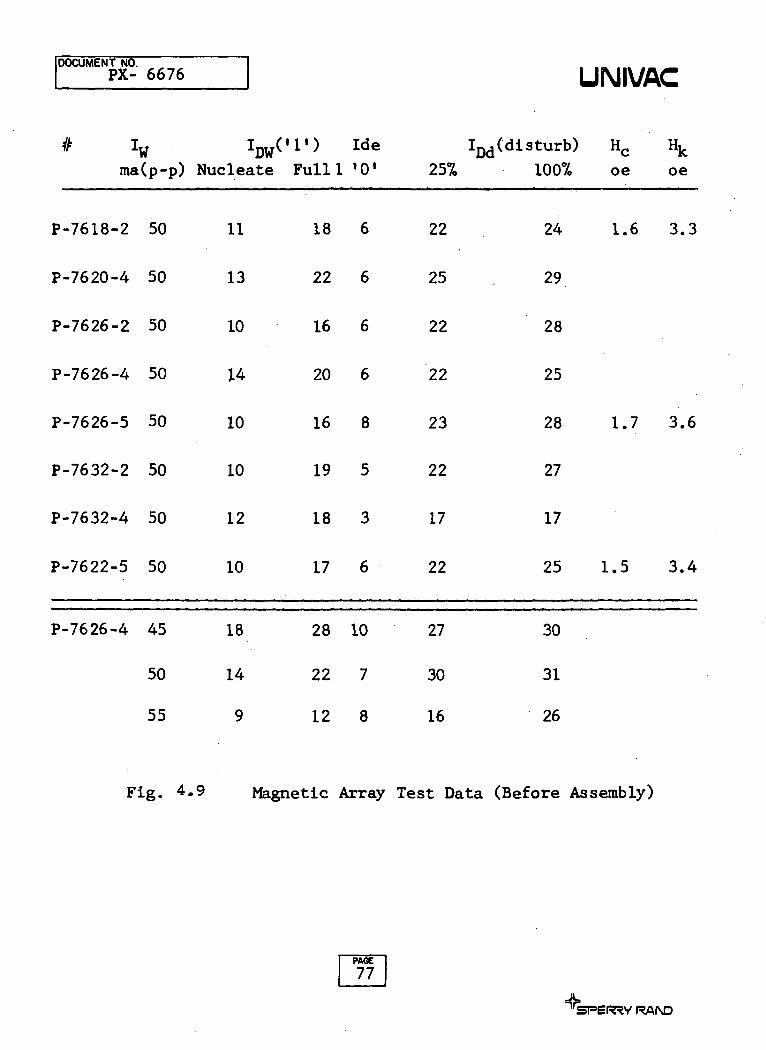
PX-6676 UNIX/ACassembly. The test data is shown in Fig. 4.9
This data shows a lower digit current I_TT touwwrite a saturated 1 than was needed during
stack evaluation testing. A larger digit line
to magnetic film spacing than that maintained
in the single bit test could yield these results,
If the digit line were significantly further
away, the field would be less for a given current
and it would spread further creating a neighbor
bit disturb problem.
4.4 Evaluation Method
a. Functional Description of Writing and Reading
The first functional criteria for any alterable
memory is the ability to write and read data.
In the oligatomic memory technology/ a logical
1 is represented by formation of a magnetic
domain in the storage media under the inter-
section of the selected word and sense digit
lines. A logical 0 is represented by no domain
formed at the intersection. If a one has been
written/ a zero is obtained by annihilation or
erasure of the domain. Therefore/ writing a
logical zero or erasing a logical one are
equivalent. In the feasibility unit/ a bipolar
digit pulse is used to minimize disturb problems
(see Section 4.5c for further explanation).
RAND
DOCUMENT NO.PX- 6676
* lw IDW01')ma(p-p) Nucleate Full 1
P-7618-2 50 11
P-7620-4 50 13
P-7626-2 50 10
P-7626-4 50 14
P-7626-5 50 10
P-7632-2 50 10
P-7632-4 50 12
'-7622-5 50 10
18
22
16
20
16
19
18
17
Ide•o1
6
6
6
6
8
5
3
6
25%
22
25
22
22
23
22
17
22
UiMIVAC
(disturb) Hc Hk100% oe oe
24 1.6 3.3
29
28
25
28 1.7 3.6
27
17
25 1.5 3.4
P-7626-4 45 18
50 14
55 9
28
22
12
10
7
8
27
30
16
30
31
26
Fig. 4.9 Magnetic Array Test Data (Before Assembly)
-feSPER3Y RAIND

DOCUMENT NO.EX-6676 UNIVAC
This means that complement data is first
written at the selected location followed
immediately by true data during the same memory
cycle.
Differential sensing is used in the feasibility
unit with the reference line or dummy shared
for each 8 active digit lines. The dummy must
remain in the logical zero state/ if information
contained in any of its 8 shared lines is to
remain accurate.
The differential output (single ended) is
gated at the second level sense-selection card
to the high gain tuned sense amplifier. The
output of the sense amplifier is detected by
an envelope detector which feeds one side of a
strobed differential comparator. The reference
side of the comparator is controlled by the
threshold voltage adjustable from the front
panel. The output of the comparator is stored
in a flip flop until the beginning of'the next
memory cycle. The flip flop output is sent
to a compare circuit which compares output data
with input data from either the pattern
generator or the input register. The non-
compared output is accumulated in the errorI PAGE
counter. 73
^SPER^Y RAIND

DOCUMENT NO.PX-6676 UNIVAC
b. Initialization
To insure that all memory arrays start with
identical dummy states/ a special write pro-
cedure called the Initialization Procedure is
used. During this procedure/ first all active
digit lines are driven by a -110 mA current
pulse which lasts for the full write cycle.
Then all the dummy digit lines are driven from
this same source. This procedure was used prior
to each evaluation test to insure that all
previous domains were erased. A low word\
current should be used or the word current
interconnect cable disconnected during this
procedure.
c. Read Zeroes
After the initialization procedure all address-
es are read. In the evaluation tests the
threshold voltage was the independent parameter/
with the error counter ouput the dependent para-
meter. After the useable range of threshold
voltage has been covered/ the test is completed
and the data is converted to graphical form.
If the input data register was set/ the output
of the error counter represents those bits greater
than or above the threshold voltage. A typical
•feSPER3Y RAND

DOCUMENT NO.
EX-6676 UNIVACRead Zero curve is shown in Fig. 4.10 if
the input register had been cleared instead/
the error counter would read all the bit outputs
below the threshold. The read zero curve is
important for two reasons 1) it shows how well
the system performs (see Sect. 4.5a Noise
Analysis) 2) it is used as a basis for com-
parison for other data.
d. Write 1's
After the initialization procedure/ and the
read zero data has been obtained/ a write all
ones program is written into all addressable
bit locations (dummy bit lines remain un-
selected except in the read mode or initiali-
zation procedure). To verify this data all
addressable bit locations are then read using
the adjustable threshold control and the error
counter output. A typical read ones curve is
also shown in Fig. 4,10.
The vertical height between the Read Zero and
Write Ones curve represents distribution of
one outputs as a function of the threshold
voltage.
This curve is also plotted in Fig. 4,10 and
is obtained the raw Write One's80 i
Hfe RAIND

DOCUMENT NO.PX - 6676 UNIVAC
Hi D
50 7<>
OOo,00) f
7777
477?--
5777
'f777--
"rrn-
.r>7i
,-rn-
177-

DOCUMENT NO.PX - 6676 UNIVAC
data from the Read Zero data.
Ideally the Read Zero and Write One curves
should be separated by a threshold gap so that
no zeroes can be misinterpreted as ones. The
slope of the Write one distribution should
initially be steep and reach a plateau of 100
percent of the bits tested for a range of
threshold voltages. A memory exhibiting this
ideal curve could be expected to have wide
operating margins (not considering disturb
phenonema).
e. Write Zeroes - Erase Ones
After writing all ones and reading their
amplitudes the next test is to restore the bits
written to the zero state. All active digit
lines are first written and then read as a
function of threshold voltage. There are
three ways to present this data 1) plot the
raw data 2) subtract the read zero data from
the raw data 3) subtract the raw data from
the write one data. All three methods were
used in the data given in the Appendix at one
time or another. Graphs of 1 or 2 are titled
Write Zeroes or Erase Ones to differentiate
the data from the Read Zero curves taken after
initialization. The third graph is titled
RAND

DOCUMENT NO.PX-6676 UNIVAC
either Writeable-Eraseable Ones or Write Ones -
Write Zeroes,
f. Curve Families
Since the best operating point for all of the bits
could only be approximated prior to the evaluation/
initial data was taken with combinations of digit
and word current as another parameter. Usually the
word current was fixed and the digit current varied
in increments by S7. Later data was taken with a
somewhat different setting of the digit currents for
each position of S7. Data taken after Jan. was ob-
tained with a different meter measuring threshold
voltage. A calibration curve for each meter is given
in the Appendix: Evaluation Data.
4.5 Functional Stack Operation
a. Noise Analysis*•
1. Random Noise
High density in a memory array usually comes at
the expense of output signal (power being fixed).
At the outset it was realized that a high gain
limited bandwidth sense system must be used to
achieve a detectable signal. Initial stack
evaluation showed on the average a saturated 1
to 0 ratio of 2:1. About 1.2 uv of rms random
noise could be expected at the sense preamplifier
input. However, the peak value of the noise
can exceed the average value many fold/ so a
safety fac aould be applied when the signal83 _i
4.'RAf\D

DOCUMENT NO.
PX-6676 UNIVACapproaches this value.
The noise at the output of the sense amplifier
with the word driver disconnected was near
500 mv (p-p). The gain of the sense amplifier-
filter combination is nearly 16,000 in the pass
band. Dividing the noise output by the gain
gave an input of 31 uv.
However, there are two additional tuned amplifier
stages ahead of the sense amplifier*
Although the cascaded gain could not be
accurately measured it was estimated to be near
10. The noise voltage referred to the input
of the sense chain would be then on the order
of 3 uv (p-p) or 1 uv rms and is then the same
as the theoretical value and cannot be signifi-
cantly reduced except by further bandwidth
limitation. If the bandwidth were reduced by a
factor of ten then the ramdom noise could be
reduced by approximately three which would be
significant.
The overall bandwidth of the sense system is
3 MHz. The initial design specification for
the sense amplifier called for 2 MHz band-
width. This had to be modified because the
time schedule and resources prohibited either
the special order from the vendor or the
IPAGE
84
rSPER3Y RA(\D

DOCUMENT NO.
PX-6676 UNIVAC
alternative of a special design/ fabrication/
and assembly effort.
The expected signal from a saturated one was
expected to be a maximum of 100 uv (p-p)
assuming a coupling factor of unity. This is
rarely achieved in practice without easy axis
flux closure as in a core or plated wire
element. The maximum true 1 signal observed
during the evaluation was 1.6 volts (p-p) which
is 10 uv when converted to the sense line out-
put. A reduction in expected signal to this
level is most logically explained by a poor
coupling factor. This could be due to an in-
effectual keeper and too great a digit line-
magnetic film spacing. A better coupling
factor or raising the sense frequency are the
only practical approaches to increasing the
signal at the same bit density.
Since the gain of the sense preamplifiers are
not precisely known/ a lower limit of 2 might
alter the above discussion. This would require
the bulk of the random noise at the sense
amplifier input to be generated in the previous
stages. The 1 uv of input noise would become
2 uv after being amplified by the preamps.
RAIXD

DOCUMENT NO.PX-6676 UNIVAC
The additional 29 uv would be generated by the
preamps. The input for a true 1 signal of 1.6
volts (p-p) would then be 50 uv (p-p). This
amount of signal reduction is more easily
explainable by a reduced coupling factor and
keeper efficiency. However/ the answer to
obtaining a better 1 to zero ratio here is a
lower noise sense gate/ preamplifier circuit.
In either case the exact gain and noise of the
sense system must be determined accurately to
determine the direction of effort to increase
the 1 signal or decrease the random noise.
2. Positional Noise
Initial evaluation testing showed that after
writing all ones a significant number could
not be verified. To isolate the problem only
one digit group was tested at a time by
removing all but the desired sense output
^cables from the second level sense selection
card. On this basis individual groups could
be found that performed better than others
but none could be observed to come close to
RAIXD

DOCUMENT NO.PX-6676 UNIVAC
even 80 percent ones. The groups were then
split in half in the word address direction.
The address counter can be set at any starting
address so Wy 1000 Wx 000 was chosen. This
was done for all six useable digit groups/ Oil
and 111 were excluded due to bad lines. Data
was first obtained from the upper half word
addresses/ then all addresses were cycled and
the differences noted. In this way data from
the near and far end of the digit line could
be identified.
Data from digit groups OOO/ 001/ and 010 (on
DSB-1- see Fig. 4.3) showed a much larger per-
centage of the bits writing on word addresses
in the first half of the register than in the
second half. They also show a read zero curve
which breaks at a higher threshold value in
the first half compared to the last half.
Thus bits written at the far end of the digit
lines could be detected better than those at
the near end. But bits at the near end had a
lower read zero threshold voltage. The bits
at the far end of the digit line are nearest
the terminated or low voltage end of the lower
word line half. Bits at the near end of the
digit line are at the high voltage end of the
•feSPER3Y RAIXD

DOCUMENT NO.PX-6676 UNIVAC
upper word line half,
Data from digit groups 100, 101 and 110 (on
DSB-4) showed a larger percentage of bits
writing on word addresses in the upper half of
the register than in the lower half. The read
zeroes curve in the lower half register broke
at a lower value of threshold voltage than
that of the upper half. The bits written at
far end of the digit line could be detected
better than those at the near end. Bits at
the near end had a lower read zero threshold
voltage. Bits at the far end of the digit
lines are nearest the low voltage end of the
upper word line half. Bits at the near end of
the digit line are at the high voltage end of
the word line half. Figure 4.11 shows
address locations of the magnetic arrays and
overlays in the stack.
The above data shows a definite and regular
dependence on position. To determine if it
was strictly a noise problem/ the common mode
word noise was investigated. An amplifier
with a gain of 6 and tuned to the word driver
frequency of 10.3 MHz was connected to each of
three digit lines on DSB-1. Figure 4.12
"SPER3Y RAI\D

DOCUMENT NO.
PX - 6676 UNIVAC
Word Addr. (Wy-Wx)
0000 - 000 ]
0011 - 111
0100 - 000
0111 - 111
1000
1011
1100
1111
f
- Ill
S/D Addr. (Dy)
111
110
101
100
Oil
010
001
000
Overlay
3 ;
Overlay
A ,
B J
4
3
6
D
E
Substrate
P7626-5
P7632-5
| P7620-4
! P7618-2
.' P7632-2iI P7632-4
P7626-4
Substrate
I P7626-5
! P7632-2
TP7632-5
JP7632-4
'P7620-4
P7626-4
TP7618-2i\ P7626-2
Fig. 4.11 Address Locations of Magnetic Arrays and Overlaysin the Stack
•feSPER^Y RftfVD

DOCUMENT NO.
PX - 6676 UNIVAC
,01 v/cm
Word Line 100 Wx
WyWord Group
0000000100100011010001010110011110001001101010111100110111101111
000011011100101110
011110000110111001011101111
Digit Line 1 Digit Line 2 Digit Line 3
1.2 .81.4 .81.2 .81.6 1.01.3 1.01.4 1.01.0 .81.0 1.12.8 .82.8 2.03.1 2.03.2 2.32.6 2.02.9 2.05.0 2.83.9 2.8
Word Line 010
1.0 .81.3 .81.2 .81.4 .91.2 .91.3 .91.0 .81.0 1.02.8 2.02.8 2.03.0 2.03.4 2.42.8 1.83.0 1.82.8 2.04.0 2.8
Digit Line 1 Digit Line 2Spare
Next 001Spare001
1.21.21.21.41.41.22.01.24.44.04.04.2•5.04.07.24.4
1,1.1,1.1.1,2,1,
22222204
4.44.04.04.44.04.03.84.4
Digit Line 3
1Oil
Fig. 4.12 Word Noise as a Function of Word Address
rSPER^V RAISD

DOCUMENT NO.EX-6676 UNIVAC
shows the relative word noise voltages
measured (1 unit = 10 mv). There are two
trends to this data 1) noise is greater in
the upper half word addresses by a factor of
3 to 4 than in the lower half. 2) Digit line
2 had an intermediate value of noise compared
to line 1 and 3 regardless of the word address.
The higher word noise occurs at word addresses
where a smaller number of bits can be written.
As would be expected the higher word noise
voltages are observed at the driven end of
the word line. The reason for a lower read
zero threshold curve for these addresses can-
not be explained by this data but may be due
to the common mode rejection ratio of the
preamp varying with frequency.
The trend of a lower noise voltage at Digit
line 2 shows that either the word current
distribution is not uniform throughout this
half of the word line or the word line im-
pedance is not uniform. The time schedule
prevented this analysis from being pursued
further than making impedance measurements of
the word and digit line with an ac bridge and
a TDR (time domain reflectometer).
JL."RAf\D
DOCUMENT NO.
PX-6676 UNIVAC3. Intersection Noise
During initial phases of evaluation testing in
the BYTE mode/ some byte addresses were ob-
served to appear to hold complement data when
actually all addresses had been written with
the same data. This could be explained by a
dummy location having changed state at the
address in question. However/ the effect was
also observed when all zeroes were written.
Since all bits do not have exactly the same
read zero output (due to sense-gate terminating
impedance variation), the complement pattern
could still be observed in some neighboring
word lines. The balance between the inputs
of the differential sense preamp depends on
both the amplitude and phase at the terminals.
This balance could be upset by the digit lines
and dummy lines shifting positions relative to
the magnetic film in a local area due to
assembly problems (dust/ adhesive thickness
variation/ etc.).
During noise reduction experiments with the
sense-digit selector (hybrid) circuit/ the
data could be changed at a normally good
position. This was done by varying the im-
pedance at the dummy or active differential
lrSPEFT?Y RAf\D

DOCUMENT NO.PX-6676 UNIVAC
input terminals on the circuit package. Thus
it was concluded that these local areas
represented a noise variation dependent on
the word line-digit line intersect spacing.
This effect is commonly called the cross-point
capacitance problem.
4. System Noise
The most common type of system noise not
previously discussed are due to ground current
loops. Operation of a memory stack with bit
outputs measured in microvolts requires a
minimum of ground loop currents to be success-
ful.
The system noise is most easily checked by
initializing and reading all zeroes at various
threshold levels. Comparison of the read zero
curves obtained in this manner will show that
they are shifted in position and have different
slopes. Much of this change is due to changes
in the grounding paths of the stack components
when in the unfolded position. For this
reason read zero data was taken just prior to
folding the memory stack for delivery and also
immediately after installation in the memory
unit. This was not done previously since it
RAIXD

DOCUMENT NO.PX - 6676 UNIVAC
was feared that too much flexure of the word
and digit overlays would cause line fractures.
Other contributions to a shift in the read zero
curve are (1) change in sense comparator reference
voltage, (2) change of meter Ml (the first one
malfunctioned halfway through evaluation requiring
a temporary substitute until a replacement was
procured) and (3) too samll or large a strobe delay
or too great a strobe width. The problem involving
the strobe delay is related to the recovery time
of the envelope detector. Selection noise at the
input of the sense amplifier drives the envelope
detector near saturation resulting in a recovery
time problem. For this reason a 20 usec cycle time
was not achieved. A redesign of the detector could
permit operation at 2-20 usec cycle time.
Another source of noise noticeable at cycle times
faster than 20 usec is the induced noise in the
sense loop caused by logic switching. The way
to eliminate this problem is to change the logic
circuit layout, and reducing the number of tim-
ing pulses traveling to and from the front panel
controls. This approach was impractical in
the feasibility model.
irSPER3Y RAND

DOCUMENT NO.EX-6676 UNIVAC
c. Read Zeroes/ Write Ones and Erase Ones Tests
1. Word and Digit Current
Initial settings of word and digit currents were
determined from the single bit data of 4.9
and from past experience during array testing.
Early tests were conducted with word currents
of 52, 56/ or 64 mA (p-p) and digit currents
of +36 -33, +30 -25, and +22 -20 mA. Later
the +36 mA was increased to +40 mA in an
attempt to write more bits.
2. Noise Reduction
Results obtained when all the sense groups were
connected were disappointing. Suspecting a
noise problem/ each digit group was investi-
gated separately and on some/ noise reduction
circuits were installed. The best noise reduction
was obtained when an inductance (which resonated
with 55 pf i 10 pf at the 20.6 MHz sense fre-
quency) was connected between ground and the
active differential preamp input. A dc isola-
tion capacitor (820 pf) was used in series with
the inductor to prevent shunting of the digit
current during the write operation.
" RAND

DOCUMENT NO.PX-6676 UNIVAC
3. Individual Group Testing
At this point it was decided to test each
digit group separately to the best operating
region of word and digit current. The
definition of "best" for these tests was the
largest number of writeable traseable bits.
In all/ 9 combinations of word and digit
current were tried for each digit group except
Oil and 111. A typical set of curves for
Dy 000 is shown in Figure 4.13 for lower half
word addresses and Fig. 4.14 for upper half
word addresses. These data were taken at the
same time with a low word current (52 mA) and
a high digit current (+35 -30 mA). Other data
in the set for the 8 other combinations
currents are in the appendix. The use of low
word and high digit current represented the
best of the 9 combinations in terms of maxi-
mum number of writeable erasable bits.
It was during the individual group testing
that the positional dependence of the data was
first noticed.
When the other 5 digit groups were checked
each showed a similar preference for a low
value of word current and a medium or high1 BASE
I 96irSPER*Y RAf\D
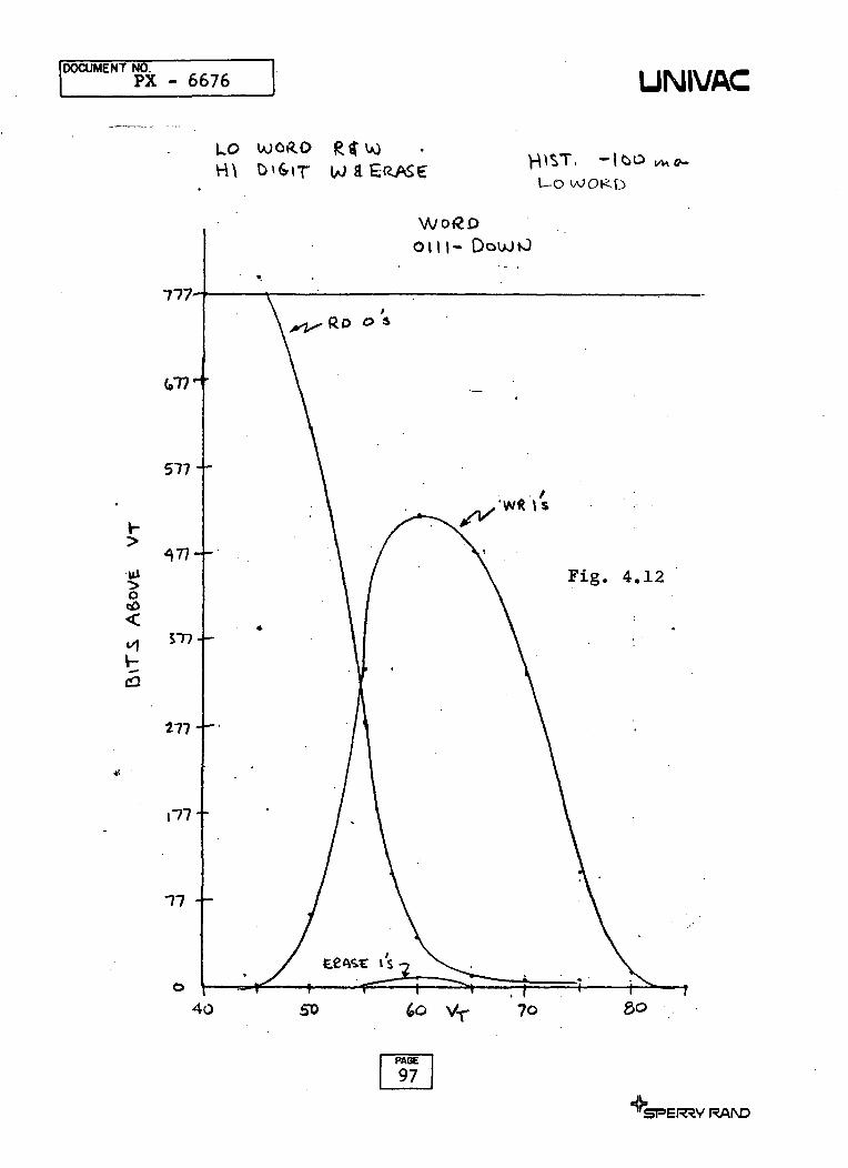
DOCUMENT NO.PX - 6676 UNIVAC
uoH\
Uo
o
7-77
(ill H-
517 --
^77--
S77--
277"
1-77 "
•77 --
irSPER^V RArvD

DOCUMENT NO.
PX - 6676 UNIVAC
LO
•777
U/ o (2 P>
OOP
Fig. 4.13
•fcSPERRV RA(\D

DOCUMENT NO.PX-6676 UNIVAC
value of digit current. Single addresses
were read at medium and high values of word
current after being initialized or written to
the one state with a low word current and a
digit current. The scope connected to the
sense amp output showed evidence of word
disturbs during continuous reads by their out-
puts suddenly increasing, decreasing, or become
unstable. Not all addresses behaved this way
but enough did so that word currents higher
than 55 mA were avoided.
This read disturb problem also occurred with
some dummy bits before the initialization
circuits were installed. At that time, the
only way the dummy could be written was with
a word current and the internal digit driver.
The digit driver could not deliver enough
current to insure that the dummy was in a
stable state so it tended to read disturb.
The 'best" individual group data was obtained on
Dy 001 where 74% of the bits wrote and erased
with a word current of 52 mA and a digit current
of +40 -30 mA. When the word current was
reduced to 45 mA, 59% of the bits wrote and
erased. These data are shown in Figs. 4.15
JL.RAND

DOCUMENT NO.
PX - 6676 UNIVAC
LoH \ r>](r\T V)
4o
PAGE
100
lrSFER5JV RAND

DOCUMENT NO.
PX-6676 UNIVACand 4.16 respectively.
3. Testing of All Useable Groups
All of the useable digit groups were tested first
as one large group and then individually prior
to folding and installing the stack in the
memory unit. In the data shown for Fig. 4.17 ,
40.5% of the addressed bits were writable and
erasable with a word current of 52mA and a
digit current of +36 -33 mA.
Later another set of data was taken on the
individual groups with a word current of 45 mA
and a digit current of +40 -30 mA. This data
given in Figs. 4.18a through 4.18d shows that
Dy 010 gave the poorest performance with only
27% of the bits writing and erasing. Groups
100, 101, and 110 showed 47% bits writing and
erasing while groups 000 and 001 showing 62.5%
of the bits writing and erasing. Overall a
maximum 40.5% of all the bits wrote and erased
with these drive currents.
Using the same values of word and digit current
as in the preceeding test the same groups were
retested after folding and installation of the
stack in the memory. This data is shown in
Figs. 4.19ar_through 4.19f . All of the
rSPER3Y RA(\D

DOCUMENT NO.
PX - 6676 UNIVAC
\\\ Ol6r IT
PAGE
102
•feSPER^Y RAI\D

DOCUMENT NO.PX - 6676 UNIVAC
Hi l/JtECJ>iSE
ALX-D\6-'T EXCEPT on
77777
PAGE
103
RA(\D

DOCUMENT NO.
PX - 6676 UNIX/AC
6.80 UPSCOJ O/Q
LPAGE
04
•feSPER^V RAIVD

DOCUME - 6676 UNIVAC
(
PAGE
105
RAfSD

DOCUMENT NO.PX - 6676 UNIVAC
/OQ

DOCUMENT NO.- DD/O UNIVAC
/oo IO/ »»o
irSPER3Y RAfSD
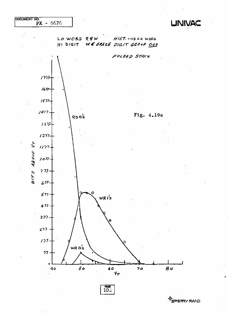
DOCUMENT NO.PX - 6676 UNIVAC
LoHI t>/<S/T
HteT. -110*0 w<?/?£>COO
Fig. 4.19a
70 80
RAI\D

"""""feT- 6676 UNIVAC
-//#
Fig. 4.19b
"SPERSY RAIXD
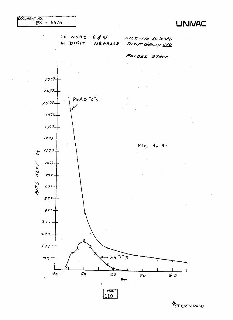
DOCUMENT NO.PX - 6676 UNIVAC
Ld
RE-AD V's
Fig. 4.19c
PAGE
noirSPERW RAf\D

DOCUMENT NO.
PX - 6676 UNIX/AC
Lo
V-•>
t*<J<tt'CvoI-
QJ
/777-
/&77-
/f77-
/477-
JP~)~
/277-
//77-
lo->7-
777-
d?->-
577-
J-)-)-
J?7-
-3.17-
m
77-
\
\ ftfAP O*5
- \
\
" \\ Fig. 4
\_ \
- \v\>ft \ ©
/ \^ ** i*
r ^^- |\ ^v" / A ^"^v
" / X- / ^^^_^^- / Jk^^ t^ft- <^5>
/ ^>^\ Y^^ — i—So Cc> , 7o 80tfr
•fcSPER^Y RAND

DOCUMENT NO.
PX - 6676 UNIX/AC
Ml D/G/T-/SO ;..
SffJ
Fig. 4.19e
PAGE
112
-fcSPER^V RA(\D

DOCUMENT NO.PX - 6676 UNIVAC
J.Q fit/S7. -/so
/^O L-£>£- /?
Fig. 4.19f
PAGE
113
'SPERSY RAM)

DOCUMENT NO.PX-6676 UNIVAC
groups except 010 showed a decrease in the
number of ones which could be erased. Group
101 showed the largest decrease in this regard.
Overall a maximum of 31% of the bits wrote and
erased after the stack was installed in the
memory unit. There are many possible explana-
tions for the change in data before and after
folding with the most plausible one being noise
introduction via ground current loops. If this
were the case/ the read zero curves should have
shifted in terms of threshold voltage or changed
shape showing a different distribution of zero
amplitudes. Comparing data for 000, 001, 100,
and 101, Fig. 4.20a after folding with 4.20b ,
the same groups before folding do not show a
large change in shape or offset. The curve for
the unfolded stack is steeper between 44 and
48 on the VT scale than the curve in the folded
condition. This should not be a contributing
factor since the write one distributions have
not reached their peak at this point.
Other explanations for the change in performance
could be a change in radiated noise or a change
in the earth's magnetic field due to a shift
in centerboard positions. All tests were
carried out in_thjPAGE
114s same room within a radius of
RAISD
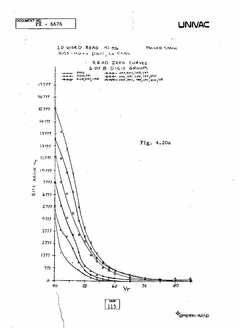
DOCUMENT NO.PX - 6676 UNIVAC
COORD READ ASI - U G r . & DI6M
000 ,00 I, lOOj |OI , O10,H0
4o
PAGE
115
RAfSD

DOCUMENT NO.PX - 6676 UNIVAC
M
Z777..
777-'
01
Fig. 4.20b
v i
"SPER3Y RAND

DOCUMENT NO.PX - 6676 UNIVAC
1 meter, the centerboards were always parallel
to the floor so a gross change in earth1s
magnetic field is unlikely. Either radiated or
ground loop noise remain the most likely choices
barring an undetected malfunction.
PAGE
117
lfSPER*Y RAIVD

DOCUMENT NO.
PX-6676 UNIVAC
4. Disturb Testing
Previous write one-erase one data showed that to
obtain the maximum number of responsive bits a
low value of word current and a high value of
digit current should be used. At this point/ the,
write digit current was increased from 36 to 40 mA
with the restore current set to 30 mA. A number
of groups were rechecked with these currents and
no substantial increase in responsive bits was
observed. At this point it was decided that a
further increase of digit current would gain
nothing so disturb testing was begun.
In the disturb test an alternate pattern of 1's
is written so that half of the memory locations are
written as a checkerboard. This pattern was
written after initialization and zeroes were read.
The alternate one pattern was read and the spaces
in the checkerboard were disturbed once with
zeroes. The ones were again read. The typical
response for any of the groups when written with
a low word and high digit current is shown in Fig.
4.21. The trend is clear, the number of bits
which were ones at any threshold value have been
cut in half; either the bits disturbed to,50%
output or half the bits disturbed to 0% output.
JL." RAI\D

DOCUMENT NO.
PX-6676 UNIVAC
A check was made to determine whether the bits
were being influenced by neighboring word or
digit lines by writing some patterns manually
in a 64 bit memory area on one substrate. The
disturb mechanism was from the adjacent bit line
rather than the word line. The digit currents
were subsequently lowered and the number of bits
which could be written to the one state were
drastically reduced. At this point/ time remain-
ing for further detailed evaluations was limited
so only general observations can be made.
An increase of digit current is required to write
the maximum number of bits.At this value a large
number of bits disturb due to the combination
self word current and neighbor digit current.
Reducing the digit current means a reduction in
the number of bits written or those which can be
read. The disturb problem is eased somewhat by
reducing the digit current. Increasing the word
current to write a maximum number of bits
is inadvisable because of the read disturb
problem. The following conclusions can be made if
noise can for a moment be neglected, 1) The
digit field spreads too far influencing the
neighbor bits, 2) Either current variations,
spacing variatjtossr; or magnetic variations prevent119)
ji_RAND
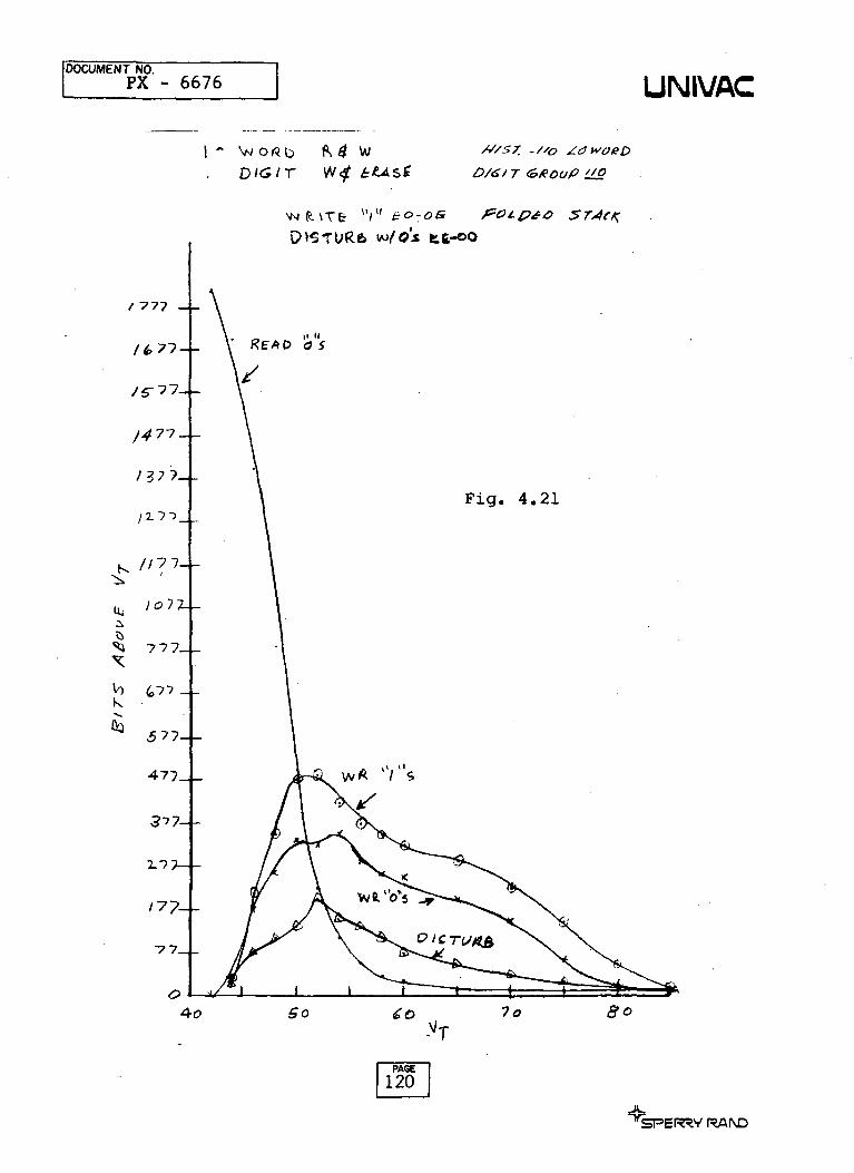
DOCUMENT NO.PX - 6676 UNIVAC
DIGIT £>/£> 7 <s>#OuP
•feSPER^V RAI\D

DOCUMENT NO.
PX-6676 UNIVAC
all bits from writing at the same value and, 3) On
the system level margins do not exist. Because
noise cannot be neglected th ese conclusions must
be qualified.
PAGE
121
•feSPER^Y RAI\D

DOCUMENT NO.
PX - 6676 UNIVAC
5.0 Conclusions
The mass memory feasibility model carried the mirror tech-
nology from the array level to the stack level. It
demonstrated feasibility of the hybrid selection electronics
and it demonstrated the low cost achievability for the
mirror memory stacks. Problems were encountered with
noise and disturb (as often occurs with the first attempt
to build an operating model with a new technology). Solutions
for these problems have been formulated and with commitment of
limited additional resources, considerable improvement of
memory operation can be achieved.
The hybrid circuit development was extremely successful,
all the circuits were fabricated on schedule with very high
yields. Only two circuit failures occurred during the
eight weeks of system evaluations. One of these circuits
could be moved and analyzed to determine the failure mode.
In addition to the good yields, it appears that the electronic
circuit density can be increased by a factor of two.
One of the most critical tasks was the fabrication of .003"
(.0076 cm) wide lines on .006" (.015 cm) centers with a length
of 44" (111.8 cm). A yield of approximately 50% was obtained
during the fabrication of these lines; however, some problems
occurred during the stack assembly and testing. During this
time 10% of the lines developed opens and shorts. Causes of
failure of these lines should be investigated.
PAGE
122
RAISD

DOCUMENT NO.
PX - 6676 UNIX/AC
The success of the read/write testing was to a great extent
masked by system noise which appears to be due to variations
in capacitance between a) the word line and the active digit
line and b) the word line and the dummy digit line (cross
point capacitance). The best octant of the memory has ap-
proximately 75% good bits in the read/write mode of testing.
It appears that this figure would be substantially increased
if the signal to noise ratio were improved. The signal could
be increased by increasing the drive frequency and by inter-
changing the position of the word and digit lines (move the
digit line to the position close to the film). The present
position of the digit line was selected on a small scale test
where the system noise was not an important factor.
There are two types of noise in the stack which appear to
be related to the cross point capacitance problem. There
is a position orientated noise in two mirror image positions
where the word line voltage is the highest. Since the cross
point capacitance noise is directly proportional to the
voltage between the word line and the digit lines, one would
expect that the cross point capacitance noise would be largest
in these areas. This could be verified by interchanging the
position of the word drive boards to see if the high noise
areas reversed.
RAND

DOCUMENT NO.PX - 6676 UNIVAC
There is also a random bit or interset noise which appears
to be related to the cross point capacitance. Verification
involves sectioning the stack to examine the dimensional
tolerances of the distance between lines. The overall noise
could be decreased by reducing the bandwidth of the sense
circuitry.
The checkboard pattern testing showed that there is an
adjacent bit disturb problem. The following techniques
could be employed to decrease this effect; turn the word
current off prior to the termination of the digit current,
increase the thickness of the ground plane, increase the
digit line spacing and use a metal substrate.
Since there are several technical problems that were defined
during the evaluation portion of this contract, it is
proposed (Section 6.0) that a new set of centerboards
be constructed and tested to verify the proposed solutions
in a modified design.
RA(\D

DOCUMENT NO.PX - 6676 UNIX/AC
6,0 Recommendations
It is recommended that the results of this first iteration
to build a mirror memory stack be applied to the design
of new centerboard assemblies. These new assemblies would
be fabricated in such a manner that they could replace the
old assemblies in the memory unit for testing and evaluating
the new design. Summarized below are the proposed tasks
for the effort.
1. Reposition the word driver boards to verify the
cause of the stack orientated noise.
2. Section the magnetic position of the stack to determine
the dimensional tolerances.
3. Perform small scale element tests to determine the
best approach or approaches to reduce the disturb
and increase the signal.
4. Construct new centerboard assemblies with the most
promising approach or approaches as defined as a
result of part 3.
5. Electronics changes
a. Terminate the word current prior to the termination
of the digit current.
b. Decrease the sense loop bandwidth.
c. Increase the word drive frequency.
6. Replace the centerboards in the feasibility model
and evaluate the new centerboard design.
PAGE
125
RAND

DOCUMENT NO.
PX - 6676 UNIVAC
7.0 Appendix
7.1 Original Data
PAGE
126
lrSPER3Y RA(\D

^ *,. <J• tu
o-£.
1 1
( I
' o
i
OH
i.-» o
127

o"
UJ
21
128Sll

<* oO '5 O> O
O
2
P
Ci3o
m
5\~uJ
Ul
<t
UJMW
129

ort
* ?Q/ I
o o^ o> o
V
O

o
o3 O
0O
UJI/I
131

lu
oo
o•<G
cQ
-- O
\-
- 0•o
Oi/)
Or
132
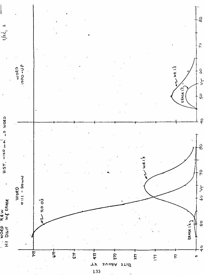
&
oBoi r

<LO oQi IO 0? °* O
. - Or-
Ǥ
134
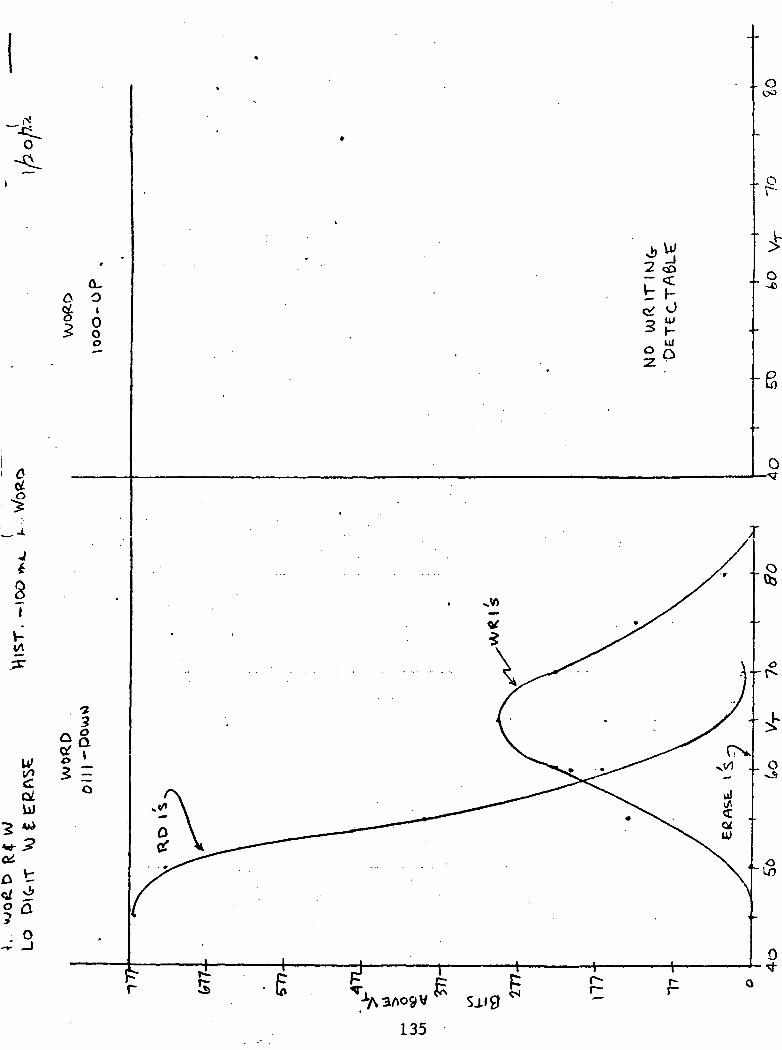
0IJ
*87
u>
oLUJ
2 ^*?<£o t«tf 2°a
135