unit iii intel 8051 microcontrollers - rgcetpdy.ac.in year/ec t53 - mpmc/unit 3.pdf · the first...
TRANSCRIPT

Department of ECE Unit 3 - RGCET
ECT53 - Microprocessors and Microcontrollers 1
UNIT III
INTEL 8051 MICROCONTROLLERS
Microcontrollers Vs Microprocessors; 8051 Architecture--Instruction set and programming;
Special Function Registers, Hardware Features –Parallel ports, Counters and Timers – Serial
I/O– Interrupts. Introduction to PIC16F877 Microcontroller- Architecture and features.
Introduction to ARM processor.
INTRODUCTION:
A decade back the process and control operations were totally implemented by the
Microprocessors only. But now a day the situation is totally changed and it is
occupied by the new devices called Microcontroller.
This microcontroller changed the embedded system design so simple and
advanced that the embedded market has become one of the most sought after for
not only entrepreneurs but for design engineers also.
With this summary Microcontrollers are,
A single chip computer or A CPU with all the peripherals like RAM, ROM, I/O Ports,
Timers, ADCs etc... on the same chip. For ex: Motorola’s 6811, Intel’s 8051, Zilog’s Z8 and
PIC 16X etc…
MICROCONTROLLERS VS MICROPROCESSORS
Microprocessor:
A CPU built into a single VLSI chip is called a microprocessor. It is a general-purpose
device and additional external circuitry is added to make it a microcomputer. The microprocessor

Department of ECE Unit 3 - RGCET
ECT53 - Microprocessors and Microcontrollers 2
contains arithmetic and logic unit (ALU), Instruction decoder and control unit, Instruction
register, Program counter (PC), clock circuit (internal or external), reset circuit (internal or
external) and registers. But the microprocessor has no on chip I/O Ports, Timers, Memory etc.
For example, Intel 8085 is an 8-bit microprocessor and Intel 8086/8088 a 16-bit microprocessor.
The block diagram of the
Microprocessor is shown in Fig.3.1
Fig.3.1 Block diagram of a Microprocessor.
MICROCONTROLLER:
A microcontroller is a highly integrated single chip, which consists of on chip CPU
(Central Processing Unit), RAM (Random Access Memory), EPROM/PROM/ROM (Erasable
Programmable Read Only Memory), I/O (input/output) – serial and parallel, timers, interrupt
controller. For example, Intel 8051 is 8-bit microcontroller and Intel 8096 is 16-bit
microcontroller. The block diagram of Microcontroller is shown in Fig.3.2.

Department of ECE Unit 3 - RGCET
ECT53 - Microprocessors and Microcontrollers 3
Fig.3.2 Block Diagram of a Microcontroller
Distinguish between Microprocessor and Microcontroller
S.No Microprocessor Microcontroller
1 A microprocessor is a general
purpose device which is called a
CPU
A microcontroller is a dedicated chip which
is also called single chip computer.
2 A microprocessor do not contain on
chip I/o Ports, Timers, Memories
etc..
A microcontroller includes RAM, ROM,
serial and parallel interface, timers,
interrupt circuitry (in addition to CPU) in a
single chip.
3 Microprocessors are most
commonly used as the CPU in
microcomputer systems
Microcontrollers are used in small,
minimum component designs performing
control-oriented applications.
4 Microprocessor instructions are
mainly nibble or byte addressable
Microcontroller instructions are both bit
addressable as well as byte addressable.
5 Microprocessor instruction sets are
mainly intended for catering to
Microcontrollers have instruction sets
catering to the control of inputs and

Department of ECE Unit 3 - RGCET
ECT53 - Microprocessors and Microcontrollers 4
large volumes of data. outputs.
6 Microprocessor based system
design is complex and expensive
Microcontroller based system design is
rather simple and cost effective
7 The Instruction set of
microprocessor is complex with
large number of instructions.
The instruction set of a Microcontroller is
very simple with less number of
instructions. For, ex: PIC microcontrollers
have only 35 instructions.
8 A microprocessor has zero status
flag
A microcontroller has no zero flag.
EVOLUTION OF MICROCONTROLLERS:
The first microcontroller TMS1000 was introduced by Texas Instruments in the year
1974. In the year 1976, Motorola designed a Microprocessor chip called 6801 which replaced
its earlier chip 6800 with certain add-on chips to make a computer. This paved the way for the
new revolution in the history of chip design and gave birth to a new entity called
“Microcontroller”. Later the Intel company produced its first Microcontroller 8048 with a
CPU and 1K bytes of EPROM, 64 Bytes of RAM an 8-Bit Timer and 27 I/O pins in 1976. Then
followed the most popular controller 8051 in the year 1980 with 4K bytes of ROM, 128 Bytes of
RAM, a serial port, two 16-bit Timers, and 32 I/O pins. The 8051 family has many additions and
improvements over the years and remains a most acclaimed tool for today’s circuit designers.
INTEL introduced a 16 bit microcontroller 8096 in the year 1982. Later INTEL introduced
80c196 series of 16-bit Microcontrollers for mainly industrial applications. Microchip, another
company has introduced an 8-bit Microcontroller PIC 16C64 in the year 1985.The 32-bit
microcontrollers have been developed by IBM and Motorola. MPC 505 is a 32-bit RISC
controller of Motorola. The 403 GA is a 32 -bit RISC embedded controller of IBM.

Department of ECE Unit 3 - RGCET
ECT53 - Microprocessors and Microcontrollers 5
In recent times ARM Company (Advanced RISC machines) has developed and introduced 32 bit
controllers for high-end application devices like mobiles, Ipods etc...
TYPES OF MICROCONTROLLERS:
Microcontrollers can be classified on the basis of internal bus width, architecture, memory and
instruction set as 4-bit, 8-bit,16-bit and 32-bit microcontrollers.
4-bit Microcontrollers:
These 4-bit microcontrollers are small size, minimum pin count and low cost controllers
which are widely used for low end applications like LED & LCD display drivers, portable
battery chargers etc.. Their power consumption is also low. The popular 4-bit controllers are
Renasa M34501 which is a 20 pin DIP chip with 4kB of ROM, 256 Bytes of RAM,2-Counters
and 14 I/O Pins. Similarly ATAM862 series from ATMEL.
8-bit Microcontrollers:
These are the most popular and widely used microcontrollers .About 55% of all CPUs
sold in the world are 8-bit microcontrollers only. The 8-bit microcontroller has 8-bitinternal bus
and the ALU performs all the arithmetic and logical operations on a byte instruction. The well
known 8-bit microcontroller is 8051 which was designed by Intel in the year 1980 for the use in
embedded systems. Other 8-bit microcontrollers are Intel 8031/8052 and Motorola MC68HC11
and AVR Microcontrollers, Microchip’s PIC Microcontrollers 12C5XX ,16C5X and 16C505
etc...
16-bit Microcontrollers:
When the microcontroller performs 16-bit arithmetic and logical operations at an
instruction, the microcontroller is said to be a 16-bit microcontroller. The internal bus width of
16-bit microcontroller is of 16-bit. These microcontrollers are having increased memory size and
speed of operation when compared to 8-bit microcontrollers. These are most suitable for

Department of ECE Unit 3 - RGCET
ECT53 - Microprocessors and Microcontrollers 6
programming in High level languages like C or C++ .They find applications in disk drivers,
modems, printers, scanners and servomotor control. Examples of 16-bit microcontrollers are
Intel 8096 family and Motorola MC68HC12 and MC68332 families, the performance and
computing capability of 16 bit microcontrollers are enhanced with greater precision as compared
to the 8-bit microcontrollers.
32-Bit Microcontrollers:
These microcontrollers used in high end applications like Automotive control,
Communication networks, Robotics, Cell phones ,GPRS & PDAs etc..For EX: PIC32, ARM 7,
ARM9, SHARP LH79520, ATMEL 32 (AVR), Texas Instrument’s –. TMS320F2802x/2803x
etc.. are some of the popular 32-bit microcontrollers.
INTEL 8051 MICRCONTROLLER:
The 8051 microcontroller is a very popular 8-bit microcontroller introduced by Intel in
the year 1981 and it has become almost the academic standard now a days. The 8051 is based on
an 8-bit CISC core with Harvard architecture. Its 8-bit architecture is optimized for control
applications with extensive Boolean processing. It is available as a 40-pin DIP chip and works at
+5 Volts DC.
The salient features of 8051 Microcontroller are
i. 4 KB on chip program memory (ROM or EPROM)).
ii. 128 bytes on chip data memory(RAM).
iii. 8-bit data bus
iv. 16-bit address bus
v. 32 general purpose registers each of 8 bits
vi. Two -16 bit timers T0 and T1
vii. Five Interrupts (3 internal and 2 external).

Department of ECE Unit 3 - RGCET
ECT53 - Microprocessors and Microcontrollers 7
ix. Four Parallel ports each of 8-bits (PORT0, PORT1, PORT2, PORT3) with a total of 32
I/O lines.
x. One 16-bit program counter and One 16-bit DPTR (data pointer)
xi. One 8-bit stack pointer
xii. One Microsecond instruction cycle with 12 MHz Crystal.
xiii. One full duplex serial communication port.
8051 ARCHITECTURE
It is 8-bit microcontroller, means MC 8051 can Read, Write and Process 8 bit data. This
is mostly used microcontroller in the robotics, home appliances like mp3 player, washing
machines, electronic iron and industries. Mostly used blocks in the architecture of 8051 are as
follows:
ALU — Arithmetic Logical Unit
This unit is used for the arithmetic calculations.
A-Accumulator
This register is used for arithmetic operations. This is also bit addressable and 8 bit register.
B-Register
This register is used in only two instructions MUL AB and DIV AB. This is also bit addressable
and 8 bit register.

Department of ECE Unit 3 - RGCET
ECT53 - Microprocessors and Microcontrollers 8
PC-Program Counter
• Points to the address of next instruction to be executed from ROM
• It is 16 bit register means the 8051 can access program address from 0000H to FFFFH. A total
of 64KB of code. 16 bit register means.
Initial value 0 0 0 0 0 0 0 0 0 0 0 0 0 0 0 0 (0000H)
Final value 1 1 1 1 1 1 1 1 1 1 1 1 1 1 1 1 (F F F FH)
• Initially PC has 0000H
• ORG instruction is used to initialize the PC ORG 0000H means PC initialize by 0000H
• PC is incremented after each instruction. ROM
8051 Flag Bits and PSW Register
→ Used to indicate the Arithmetic condition of ACC.
→ Flag register in 8051 is called as program status word (PSW). This special function register
PSW is also bit addressable and 8 bit wide means each bit can be set or reset independently.

Department of ECE Unit 3 - RGCET
ECT53 - Microprocessors and Microcontrollers 9
The bits PSW3 and PSW4 are denoted as RS0 and RS1 and these bits are used to select the bank
registers of the RAM location. The meaning of various bits of PSW register is shown below.
CY PSW0.7 Carry Flag
AC PSW0.6 Auxiliary Carry Flag
F0 PSW0.5 Flag 0 available for general purpose.
RS1 PSW0.4 Register Bank select bit 1
RS0 PSW0.3 Register bank select bit 0
OV PSW0.2 Overflow flag
--- PSW0.1 User definable flag
P PSW0.0 Parity flag .set/cleared by hardware.
• P → Parity flag → PSW 0.0
1 – odd number of 1 in ACC
0 – even number of 1 in ACC
• OV (PSW 0.2) → overflow flag → this is used to detect error in signed arithmetic operation.
This is similar to carry flag but difference is only that carry flag is used for unsigned operation.
The selection of the register Banks and their addresses are given below.
RS1 RS0 Register Bank Address
0 0 0 00H-07H
0 1 1 08H-0FH
1 0 2 10H-17H
1 1 3 18H-1FH

Department of ECE Unit 3 - RGCET
ECT53 - Microprocessors and Microcontrollers 10
Initially by default always Bank 0 is selected.
• F0 → user definable bit
• AC → Auxiliary carry flag → when carry is generated from D3 to D4, it is set to 1, it is used in
BCD arithmetic.
Since carry is generated from D3 to D4, so AC is set.
•CY → carry flag → Affected after 8 bit addition and subtraction. It is used to detect error in
unsigned arithmetic operation. We can also use it as single bit storage.
SETB C → for cy = 1
CLR C → for cy = 0
Stack in 8051
→ RAM locations from 08H to 1FH can be used as stack. Stack is used to store the data
temporarily.
Stack is last in first out (LIFO)
→ Stack pointer (SP)
• 8bit register
• It indicates current RAM address available for stack or it points the top of stack.
• Initially by default at 07H because first location of stack is 08H.
• After each PUSH instruction the SP is incremented by one while in MC after PUSH instruction
SP is decremented.
• After each POP instruction the SP is decremented.
DPTR Data Pointer in 8051
16 bit register, it is divided into two parts DPH a
DPH for Higher order 8 bits, DPL for lower order

Department of ECE Unit 3 - RGCET
ECT53 - Microprocessors and Microcontrollers 11
DPTR, DPH, DPL these all are SFRs in 8051.
PIN DIAGRAM OF 8051:
The 8051 microcontroller is available as a 40 pin DIP chip and it works at +5 volts DC.
•VCC → 5V supply
• VSS → GND
• XTAL2/XTALI are for oscillator input
• Port 0 – 32 to 39 – AD0/AD7 and P0.0 to P0.7
• Port 1 – 1 to 8 – P1.0 to P1.7
• Port 2 – 21 to 28 – P2.0 to P2.7 and A 8 to A15
• Port 3 – 10 to 17 – P3.0 to P3.7
• P 3.0 – RXD – Serial data input – SBUF
• P 3.1 – TXD – Serial data output – SBUF
• P 3.2 – INT0 – External interrupt 0 – TCON 0.1

Department of ECE Unit 3 - RGCET
ECT53 - Microprocessors and Microcontrollers 12
• P 3.3 – INT1 – External interrupt 1 – TCON 0.3
• P 3.4 – T0 – External timer 0 input – TMOD
XTAL1, XTAL2:
These two pins are connected to Quartz crystal oscillator which runs the on-chip
oscillator. The quartz crystal oscillator is connected to the two pins along with a capacitor of
30pF as shown in the circuit. If we use a source other than the crystal oscillator, it will be
connected to XTAL1 and XTAL2 is left unconnected.
P0.0- P0.7(AD0-AD7) : The port 0 pins multiplexed with Address/data pins .If the
microcontroller is accessing external memory these pins will act as address/data pins otherwise
they are used for Port 0 pins.
P2.0- P2.7(A8-A15) : The port2 pins are multiplexed with the higher order address pins .When
the microcontroller is accessing external memory these pins provide the higher order address
byte otherwise they act as Port 2 pins.
P1.0- P1.7: These 8-pins are dedicated for Port1 to perform input or output port operations.
P3.0- P3.7: These 8-pins are meant for Port3 operations and also for some control operations
like Read, Write, Timer0, Timer1, INT0, INT1, RxD and TxD

Department of ECE Unit 3 - RGCET
ECT53 - Microprocessors and Microcontrollers 13
RST: The RESET pin is an input pin and it is an active high pin. When a high pulse is applied to
this pin the microcontroller will reset and terminate all activities. Upon reset all the registers
except PC will reset to 0000 Value and PC register will reset to 0007 value.
(External Access): This pin is an active low pin. This pin is connected to ground when
microcontroller is accessing the program code stored in the external memory and connected to
Vcc when it is accessing the program code in the on chip memory. This pin should not be left
unconnected.
(Program Store Enable): This is an output pin which is active low. When the
microcontroller is accessing the program code stored in the external ROM, this pin is connected
to the OE (Output Enable) pin of the ROM.
ALE (Address latch enable): This is an output pin, which is active high. When connected to
external memory , port 0 provides both address and data i.e address and data are multiplexed
through port 0 .This ALE pin will demultiplex the address and data bus .When the pin is High ,
the AD bus will act as address bus otherwise the AD bus will act as Data bus.
Input Output Ports
• There are four input output ports available P0, P1, P2, P3.
• Each port is 8 bit wide and has special function register P0, P1, P2, P3 which are bit
addressable means each bit can be set or reset by the Bit instructions (SETB for high, CLR for
low) independently.
• The data at any port which is transmitting or receiving is in these registers.
• The port 0 can perform dual works. It is also used as Lower order address bus (A0 to A7)
multiplexed with 8 bit data bus P0.0 to P0.7 is AD0 to AD7 respectively the address bus and data
bus is demultiplexed by the ALE signal and latch which is further discussed in details.
• Port 2 can be used as I/O port as well as higher order address bus A8 to A15.
• Port 3 also have dual functions it can be worked as I/O as well as each pin of P3 has specific
function.
P3.0 – RXD – {Serial I / P for Asynchronous communication
Serial O / P for synchronous communication}.

Department of ECE Unit 3 - RGCET
ECT53 - Microprocessors and Microcontrollers 14
P3.1 – TXD – Serial data transmit.
P3.2 – INT0 – External Interrupt 0.
P3.3 – INT1 – External Interrupt 1.
P3.4 – T0 – Clock input for counter 0.
P3.5 – T1 – Clock input for counter 1.
P3.6 – WR – Signal for writing to external memory.
P3.7 – RD – Signal for reading from external memory.
When external memory is interfaced with 8051 then P0 and P2 can’t be worked as I/O port they
works as address bus and data bus, otherwise they can be accessed as I/O ports.
Oscillator
• It is used for providing the clock to MC8051 which decides the speed or baud rate of MC.
• We use crystal which frequency vary from 4MHz to 30 MHz, normally we use 11.0592 MHz
frequency.
Interrupts
• Interrupts are defined as requests because they can be refused (masked) if they are not used,
that is when an interrupt is acknowledged. A special set of events or routines are followed to
handle the interrupts. These special routines are known as interrupt handler or interrupt service
routines (ISR).
These are located at a special location in memory.
• INT0 and INT1 are the pins for external interrupts.
Timers and Counters
Timer means which can give the delay of particular time between some events. For
example on or off the lights after every 2 sec. This delay can be provided through some assembly
program but in microcontroller two hardware pins are available for delay generation. These
hardware pins can be also used for counting some external events. How much time a number is
repeated in the given table is calculated by the counter?

Department of ECE Unit 3 - RGCET
ECT53 - Microprocessors and Microcontrollers 15
• In MC8051, two timer pins are available T0 and T1, by these timers we can give the delay of
particular time if we use these in timer mode.
• We can count external pulses at these pins if we use these pins in counter mode.
• 16 bits timers are available. Means we can generate delay between 0000H to FFFFH.
• Two special function registers are available.
If we want to load T0 with 16 bit data then we can load separate lower 8 bitin TL0 and
higher 8 bit in TH0.
• In the same way for T1.
• TMOD, TCON registers are used for controlling timer operation.
Memory organization:
The 8051 microcontroller has 128 bytes of Internal RAM and 4kB of on chip ROM .The
RAM is also known as Data memory and the ROM is known as program memory. The program
memory is also known as Code memory .This Code memory holds the actual 8051 program that
is to be executed. In 8051 this memory is limited to 64K .Code memory may be found on-chip,
as ROM or EPROM. It may also be stored completely off-chip in an external ROM or, more
commonly, an external EPROM. The 8051 has only 128 bytes of Internal RAM but it supports
64kB of external RAM. As the name suggests, external RAM is any random access memory
which is off-chip. Since the memory is off-chip it is not as flexible interms of accessing, and is
also slower. For example, to increment an Internal RAM location by 1,it requires only 1

Department of ECE Unit 3 - RGCET
ECT53 - Microprocessors and Microcontrollers 16
instruction and 1 instruction cycle but to increment a 1-byte value stored in External RAM
requires 4 instructions and 7 instruction cycles. So, here the external memory is 7 times slower.
Internal RAM OF 8051:
This Internal RAM is found on-chip on the 8051 .So it is the fastest RAM available, and
it is also the most flexible in terms of reading, writing, and modifying it’s contents. Internal
RAM is volatile, so when the 8051 is reset this memory is cleared. The 128 bytes of internal
RAM is organized as below.
(i) Four register banks (Bank0, Bank1, Bank2 and Bank3) each of 8-bits (total 32 bytes). The
default bank register is Bank0. The remaining Banks are selected with the help of RS0 and
RS1 bits of PSW Register.
(ii) 16 bytes of bit addressable area and
(iii) 80 bytes of general purpose area (Scratch pad memory) as shown in the diagram below.
This area is also utilized by the microcontroller as a storage area for the operating stack.

Department of ECE Unit 3 - RGCET
ECT53 - Microprocessors and Microcontrollers 17
The 32 bytes of RAM from address 00 H to 1FH are used as working registers organized as four
banks of eight registers each. The registers are named as R0-R7 .Each register can be addressed
by its name or by its RAM address.
For EX: MOV A, R7 or MOV R7, #05H
On chip ROM
In 8051, 4KB read only memory (ROM) is available for program storage. This is used for
permanent data storage. Or the data which is not changed during the processing like the program
or algorithm for specific applications.
• This is volatile memory; the data saved in this memory does not disappear after power failure.
• We can interface up to 64KB ROM memory externally if the application is large. These sizes
are specified different by their companies.
• Address Range of PC: Address range of PC means program counter (which points the next
instruction to be executing) can be moved between these locations or we can save the program
from this location to this location. The address range can be calculated in the same way just like
the RAM which is discussed in previous section
.
Address range of PC is 0000H to 0FFFH means total 4KB locations are available from 0000H to
0FFFH.

Department of ECE Unit 3 - RGCET
ECT53 - Microprocessors and Microcontrollers 18
SPECIAL FUNCTION REGISTERS (SFRs):
In 8051 microcontroller there certain registers which uses the RAM addresses from 80h
to FFh and they are meant for certain specific operations .These registers are called Special
function registers (SFRs).Some of these registers are bit addressable also.
The list of SFRs and their functional names are given below. In these SFRs some of them are
related to I/O ports (P0,P1,P2 and P3) and some of them are meant for control operations
(TCON,SCON, PCON..) and remaining are the auxiliary SFRs, in the sense that they don't
directly configure the 8051.
S.No Symbol Name of SFR Address (Hex)
1 ACC* Accumulator 0E0
2 B* B-Register 0F0
3 PSW* Program Status word register 0DO
4 SP Stack Pointer Register 81
5
DPTR
DPL Data pointer low byte 82
DPH Data pointer high byte 83
6 P0* Port 0 80
P1* Port 1 90
8 P2* Port 2 0A
9 P3* Port 3 0B
10 IP* Interrupt Priority control 0B8
11 IE* Interrupt Enable control 0A8
12 TMOD Tmier mode register 89
13 TCON* Timer control register 88
14 TH0 Timer 0 Higher byte 8C

Department of ECE Unit 3 - RGCET
ECT53 - Microprocessors and Microcontrollers 19
15 TL0 Timer 0 Lower byte 8A
16 TH1 Timer 1Higher byte 8D
17 TL1 Timer 1 lower byte 8B
18 SCON* Serial control register 98
19 SBUF Serial buffer register 99
20 PCON Power control register 87
The * indicates the bit addressable SFRs
Table:SFRs of 8051 Microcontroller
PARALLEL I /O PORTS :
The 8051 microcontroller has four parallel I/O ports , each of 8-bits .So, it provides the
user 32 I/O lines for connecting the microcontroller to the peripherals. The four ports are P0
(Port 0), P1(Port1) ,P2(Port 2) and P3 (Port3). Upon reset all the ports are output ports. In order
to make them input, all the ports must be set i.e a high bit must be sent to all the port pins. This
is normally done by the instruction “SETB”.
Ex: MOV A,#0FFH ; A = FF
MOV P0,A ; make P0 an input port
PORT 0:
Port 0 is an 8-bit I/O port with dual purpose. If external memory is used, these port pins
are used for the lower address byte address/data (AD0-AD7), otherwise all bits of the port are
either input or output.. Unlike other ports, Port 0 is not provided with pull-up resistors internally
,so for PORT0 pull-up resistors of nearly 10k are to be connected externally as shown in the
fig.2.
Dual role of port 0:
Port 0 can also be used as address/data bus (AD0-AD7), allowing it to be used for both
address and data. When connecting the 8051 to an external memory, port 0 provides both address
and data. The 8051 multiplexes address and data through port 0 to save the pins. ALE indicates

Department of ECE Unit 3 - RGCET
ECT53 - Microprocessors and Microcontrollers 20
whether P0 has address or data. When ALE = 0, it provides data D0-D7, and when ALE =1 it
provides address and data with the help of a 74LS373 latch.
Port 1:
Port 1 occupies a total of 8 pins (pins 1 through 8). It has no dual application and acts
only as input or output port. In contrast to port 0, this port does not need any pull-up resistors
since pull-up resistors connected internally. Upon reset, Port 1 is configured as an output port. To
configure it as an input port, port bits must be set i.e a high bit must be sent to all the port pins.
This is normally done by the instruction “SETB”.
For Ex:
MOV A, #0FFH ; A=FF HEX
MOV P1, A ; make P1 an input port by writing 1’s to all of its pins
Port 2 :
Port 2 is also an eight bit parallel port. (pins 21- 28). It can be used as input or output
port. As this port is provided with internal pull-up resistors it does not need any external pull-up
resistors. Upon reset, Port 2 is configured as an output port. If the port is to be used as input port,
all the port bits must be made high by sending FF to the port. For ex,
MOV A, #0FFH ; A=FF hex
MOV P2, A ; make P2 an input port by writing all 1’s to it
Dual role of port 2:

Department of ECE Unit 3 - RGCET
ECT53 - Microprocessors and Microcontrollers 21
Port2 lines are also associated with the higher order address lines A8-A15. In systems
based on the 8751, 8951, and DS5000, Port2 is used as simple I/O port.. But, in 8031-based
systems, port 2 is used along with P0 to provide the 16-bit address for the external memory.
Since an 8031 is capable of accessing 64K bytes of external memory, it needs a path for the 16
bits of the address. While P0 provides the lower 8 bits via A0-A7, it is the job of P2 to provide
bits A8-A15 of the address. In other words, when 8031 is connected to external memory, Port 2
is used for the upper 8 bits of the 16 bit address, and it cannot be used for I/O operations.
PORT 3:
Port3 is also an 8-bit parallel port with dual function.( pins 10 to 17). The port pins can
be used for I/O operations as well as for control operations. The details of these additional
operations are given below in the table. Port 3 also do not need any external pull-up resistors as
they are provided internally similar to the case of Port2 & Port 1. Upon reset port 3 is
configured as an output port . If the port is to be used as input port, all the port bits must be made
high by sending FF to the port. For ex,
MOV A, #0FFH ; A= FF hex
MOV P3, A ; make P3 an input port by writing all 1’s to it
Alternate Functions of Port 3:
P3.0 and P3.1 are used for the RxD (Receive Data) and TxD (Transmit Data) serial
communications signals. Bits P3.2 and P3.3 are meant for external interrupts. Bits P3.4 and P3.5
are used for Timers 0 and 1 and P3.6 and P3.7 are used to provide the write and read signals of
external memories connected in 8031 based systems
S.No Port 3 bit Pin No Function
1 P3.0 10 RxD
2 P3.1 11 TxD
3 P3.2 12

Department of ECE Unit 3 - RGCET
ECT53 - Microprocessors and Microcontrollers 22
4 P3.3 13
5 P3.4 14 T0
6 P3.5 15 T1
7 P3.6 16
8 P3.7 17
Table: PORT 3 alternate functions
INSTRUCTION SET
ADDRESSING MODES OF 8051:
The way in which the data operands are accessed by different instructions is known as the
addressing modes. There are various methods of denoting the data operands in the instruction.
The 8051 microcontroller supports mainly 5 addressing modes.
They are
1. Immediate addressing mode
2. Direct Addressing mode
3. Register addressing mode
4. Register Indirect addressing mode
5. Indexed addressing mode
Immediate addressing mode:
The addressing mode in which the data operand is a constant and
it is a part of the instruction itself is known as Immediate addressing mode. Normally the data
must be preceded by a # sign. This addressing mode can be used to transfer the data into any of
the registers including DPTR.
Ex: MOV A, # 27 H : The data (constant) 27 is moved to the accumulator register
ADD R1, #45 H: Add the constant 45 to the contents of the accumulator
MOV DPTR, # 8245H: Move the data 8245 into the data pointer register.

Department of ECE Unit 3 - RGCET
ECT53 - Microprocessors and Microcontrollers 23
MOV P1, #21 H
Direct addressing mode:
The addressing mode in which the data operand is in the RAM
location (00 -7FH) and the address of the data operand is given in the instruction is known as
Direct addressing mode. The direct addressing mode uses the lower 128 bytes of Internal RAM
and the SFRs
MOV R1, 42H : Move the contents of RAM location 42 into R1 register
MOV 49H, A: Move the contents of the accumulator into the RAM location 49.
ADD A, 56H: Add the contents of the RAM location 56 to the accumulator
Register addressing mode:
The addressing mode in which the data operand to be
manipulated lies in one of the registers is known as register addressing mode.
MOV A, R0: Move the contents of the register R0 to the accumulator
ADD A, R6: Add the contents of R6 register to the accumulator
MOV P1, R2: Move the contents of the R2 register into port 1
MOV R5, R2: This is invalid .The data transfer between the registers is not allowed.
Register indirect addressing mode:
The addressing mode in which a register is used as a pointer to
the data memory block is known as Register indirect addressing mode.
MOV A, @ R0: Move the contents of RAM location whose address is in R0 into A
(accumulator)

Department of ECE Unit 3 - RGCET
ECT53 - Microprocessors and Microcontrollers 24
MOV @ R1, B: Move the contents of B into RAM location whose address is held by R1
When R0 and R1 are used as pointers, they must be preceded by @ sign
One of the advantages of register indirect addressing mode is that it makes accessing the
data more dynamic than static as in the case of direct addressing mode.
Indexed addressing mode:
This addressing mode is used in accessing the data elements of
lookup table entries located in program ROM space of 8051.
Ex: MOVC A,@ A+DPTR
The 16-bit register DPTR and register A are used to form the address of the data element stored
in on-chip ROM. Here C denotes code .In this instruction the contents of An are added to the
16-bit DPTR register to form the 16-bit address of the data operand.
8051 ASSEMBLY LANGUAGE PROGRAMMING
A program to find sum of N natural numbers and store the sum
Program description:- The number “N” is stored in location 35H. Natural numbers generated
from 0 to N must be stored from location 55H. The sum of natural numbers must be stored in
location 36H.
Analyzing the program description, we need 3 registers. R0 to store the value of “N” (given in
location 35H)and to act as a counter for generating natural numbers up to N. R5 is used to save
the value of first storage location of natural numbers and then R5 is incremented by one each to
store each newly generated natural number. R7 is initiated as 0 and is incremented by 1 to
generate natural numbers.
The Program:-
MOV PSW, #00H / Register bank '0' is selected by executing this instruction.
MOV R0, 35H // the value of 'N' stored in location 35H is transferred to R0.
MOV R5, #55H // The starting location for storing natural numbers '#55H' is transferred to
R5

Department of ECE Unit 3 - RGCET
ECT53 - Microprocessors and Microcontrollers 25
MOV A, #00H // Accumulator is initiated with value 0 for adding natural numbers
cumulatively.
MOV R7, #00H // R7 is initialized to '0' to generate natural numbers. Note: '0' is not a
natural number.
LOOP: INC R7 // R7 is incremented by 1 to generate next natural number.
MOV @R5, 07H // this is indirect addressing mode used here. It is not possible to transfer
data from one register to another register directly. So an instruction like MOV R5, R7 is invalid.
Instead we use the direct address (07) of register R7 of register bank #00 to transfer the
generated natural number to it's storage location in register R5.Indirect addressing is used as we
need to save the generated natural number directly to memory address. R5 holds the starting
location address (of the storage area) as its value i.e #55H.By indirectly addressing, we can save
what ever value in R7 directly to location #55H.
INC R5 // The storage location is incremented by 1 from #55H to #56H to store the next
generated natural number
ADD A, R7 // the generated natural number is added to contents in accumulator.
DJNZ R0, LOOP // the value of register Ro (value of 'N') is decremented by 1. It is checked
against stopping condition zero. If it’s R0 is not equal to zero, the program control will move to
label LOOP again and the steps from INC R7 will be executed again until R0 is equal to zero.
When R0 is equal to zero, program control will exit the loop and move to next instruction given
below.
MOV 36H, A // the sum of natural numbers in accumulator is moved to storage location 36H.
STOP: SJMP STOP // an infinite loop written at the end of the program. When this instruction
is reached program control will get stuck at this instruction as it's an infinite loop.To get out of
this infinite loop system reset must be applied.
A simple program to copy a block of data from one location to another
Program Description:- 10 bytes of data stored from 30H is to be copied to another location
staring from 50H.
Analyzing the program, two registers are needed to store starting locations of source and
destination. Let’s say we take R0 as the source and R2 as the destination registers. Now we need
a counter to count 10 bytes of data transferred from source to destination. Let’s take R3 for that.
It is not possible to transfer data from one register to another register directly by using any kind

Department of ECE Unit 3 - RGCET
ECT53 - Microprocessors and Microcontrollers 26
of addressing mode. So we need accumulator to stand in between as a temporary register. So
here is it:
The Program:
MOV R0, #30H // Address of the starting location of source data is moved to R0.
MOV R1, #50H // Address of the starting location of destination is moved to R1
MOV R3, #OAH // Set the counter R3 with 10. You can also use decimal number as MOV
R3, #10d.
LOOP: MOV A, @R0 // Indirect addressing mode is used. Contents at the location of Ro
(30H) are copied to accumulator.
MOV @R1, A // Contents in accumulator is copied to location pointed by Ra (that is
50H).
INC R0 // Ro is incremented by 1 to point to next location.
INC R1 // R1 is incremented by 1 to point to next location.
DJNZ R3, LOOP // Counter register R3 is decremented by 1 and checked against zero. See
the explanation DJNZ in the first program "sum of natural numbers"
STOP: SJMP STOP // Infinite loop to terminate program
To generate a Fibonacci series
Program description:- A Fibonacci series is an infinite series in mathematics that goes like
0,1,1,2,3,5,8,13,21….
Write a program which generates Fibonacci series up to N terms. The value of N is available in
location 30H and to save the series from location 40H.
The Program:-
BEGIN: MOV R1, 30H // Getting the value of "N"
MOV R7, #40H // The first number '0' of series is stored here.
MOV @R7,#00H // Loading value 'o' to address 40H using indirect addressing
INC R7 // Incrementing value of R7 from 40H to 41H to store next number '1'

Department of ECE Unit 3 - RGCET
ECT53 - Microprocessors and Microcontrollers 27
MOV @R7, #01H // Storing value '1' to location 41H. Note that 'o' and '1' are seed values of a
Fibonacci series and has to be generated manually.
MOV R5,#42H // New register R5 is loaded with location address 42H to store next values
of series, generated by adding the 2 previously generated numbers.
DEC R1
DEC R1 // the count value "N" is decremented by 2, as we have already generated and
stored 1st two numbers.
DEC R7 // R7 is now reduced from 41H to 40H. We need to add contents of 40H and 41 H
to get the number that is to be stored in 42H.
LOOP: MOV A, @R7 // Contents in R7 is moved to accumulator.
INC R7 // R7 is incremented to get the next value.
ADD A,@R7 // The two values are added and stored in Acc.
MOV @R5, A //The newly generated value of the series is stored in the address held by R5.
INC R5 // R5 is incremented to store next value.
DJNZ R1, LOOP // The count "N" is checked to zero (to know if all the numbers up to N
are generated).
STOP: SJMP STOP // Run infinitely here or end of program execution.
COUNTERS AND TIMERS
The 8051 microcontroller has two 16-bit timers Timer 0 (T0) and Timer 1(T1) which can
be used either to generate accurate time delays or as event counters. These timers are accessed
as two 8-bit registers TLO, THO & TL1 ,TH1 because the 8051 microcontroller has 8-bit
architecture.
Counting/timing device as timer:
A device for timing when the inputs to counting are given by a clock. The clock pulses
are internally given at the specific time intervals in case of functioning as timer.
Counting/timing device as counter:
A device for counting when the inputs to count are given externally. Counter is given the
input to count from external input pin.

Department of ECE Unit 3 - RGCET
ECT53 - Microprocessors and Microcontrollers 28
Counting/timing device External controls for activation or deactivation of running:
When timing or counting devices is externally controlled by the gate input, when GT0 or
GT1 is externally activated the device can function else it deactivates in gate input mode. GT0 or
GT1 signals are given at P3.2 and P3.3.
Counting/timing device External count inputs in counter mode:
T0 counts the T0 is given the input to count from external input pin T0at P3.4.T1 counts
when T1 is given the input to count from external input pin T1at P3.5.
Four Port P3 Pin functions:
P3.2, P3.3, P3.4 and P3.5 When TMOD SFR bits 3, 7, 2 and 6 set = 1, function asGT0
(gate for starting/stopping T1), GT1 (gate for starting/stopping T1), T0 (count input to T0) and
T1 (count input to T1) inputs, respectively
TIMER 0:
The Timer 0 is a 16-bit register and can be treated as two 8-bit registers (TL0 & TH0)
and these registers can be accessed similar to any other registers like A,B or R1,R2,R3 etc…
Ex: The instruction Mov TL0, #07 moves the value 07 into lower byte of Timer0.
Similarly Mov R5, TH0 saves the contents of TH0 in the R5 register.
TIMER 1:
The Timer 1 is also a 16-bit register and can be treated as two 8-bit registers (TL1 &
TH1) and these registers can be accessed similar to any other registers like A,B or R1,R2,R3
etc…
Ex: The instruction MOV TL1, #05 moves the value 05 into lower byte of Timer1.
Similarly MOV R0, TH1 saves the contents of TH1 in the R0 register

Department of ECE Unit 3 - RGCET
ECT53 - Microprocessors and Microcontrollers 29
TMOD Register:
The various operating modes of both the timers T0 and T1 are set by an 8-bit register
called TMOD register. In this TMOD register the lower 4-bits are meant for Timer 0 and the
higher 4-bits are meant for Timer1.
GATE:
This bit is used to start or stop the timers by hardware .When GATE= 1, the timers can be
started / stopped by the external sources. When GATE= 0, the timers can be started or stopped
by software instructions like SETB TR0 or SETB TR1
C/T (clock/Timer):
This bit decides whether the timer is used as delay generator or event counter. When C/T
= 01, the Timer is used as delay generator and if C/T=1 the timer is used as an event counter.
The clock source for the time delay is the crystal frequency of 8051.
M1, M0 (Mode):
These two bits are the timer mode bits. The timers of the 8051 can be configured in three
modes.Mode0, Mode1 and Mode2.The selection and operation of the modes is shown below.
S.No M0 M1 Mode Operation
1 0 0 0 13-bit Timer mode
8-bit Timer/counter. THx with TLx as 5-bit
prescalar
2 0 1 1 16-bit Timer mode.16-bit timer /counter
without pre-scalar
3 1 0 2 8-bit auto reload. THx contains a value that
is to be loaded into TLx each time it
overflows
4 1 1 3 Split timer mode

Department of ECE Unit 3 - RGCET
ECT53 - Microprocessors and Microcontrollers 30
SERIAL I/O Serial Port:
There are two pins available for serial communication TXD and RXD.
Normally TXD is used for transmitting serial data which is in SBUF register,
RXD is used for receiving the serial data.
SCON register is used for controlling the operation.
There are four modes of serial communication which has been discussed in next chapter. banks
and stack. But other 128 byte RAM which consists of SFRs. We will discuss the RAM in detail
in next section.
Now what is the meaning of 128 byte RAM. What are address range which is provided for data
storage. We will discuss here.
We know that 128 byte = 27 Byte
Since 27
Bytes so last 7 bits can be changed so total locations are from 00H to 7F H. This
procedure of calculating the memory address is called as “memory mapping”. We can save data
on memory locations from 00H to 7FH. Means total 128 byte space from 00H to 7FH is provided
for data storage.
INTERRUPTS.
An interrupt is an external or internal event that disturbs the microcontroller to inform it
that a device needs its service. The program which is associated with the interrupt is called the
interrupt service routine (ISR) or interrupt handler. Upon receiving the interrupt signal the
Microcontroller, finish current instruction and saves the PC on stack. Jumps to a fixed location
in memory depending on type of interrupt Starts to execute the interrupt service routine until
RETI (return from interrupt) upon executing the RETI the microcontroller returns to the place
where it was interrupted. Get pop PC from stack
The 8051 microcontroller has FIVE interrupts in addition to Reset. They are

Department of ECE Unit 3 - RGCET
ECT53 - Microprocessors and Microcontrollers 31
Timer 0 overflow Interrupt
Timer 1 overflow Interrupt
External Interrupt 0(INT0)
External Interrupt 1(INT1)
Serial Port events (buffer full, buffer empty, etc) Interrupt
Each interrupt has a specific place in code memory where program execution (interrupt service
routine) begins.
External Interrupt 0: 0003 H
Timer 0 overflow: 000B H
External Interrupt 1: 0013 H
Timer 1 overflow: 001B H
Serial Interrupt : 0023 H
Upon reset all Interrupts are disabled & do not respond to the Microcontroller. These interrupts
must be enabled by software in order for the Microcontroller to respond to them. This is done by
an 8-bit register called Interrupt Enable Register (IE).
Interrupt Enable Register:
EA : Global enable/disable. To enable the interrupts this bit must be set High.
--- : Undefined-reserved for future use.
ET2: Enable /disable Timer 2 overflow interrupt.
ES : Enable/disable Serial port interrupts.
ET1: Enable /disable Timer 1 overflow interrupt.
EX1: Enable/disable External interrupt1.

Department of ECE Unit 3 - RGCET
ECT53 - Microprocessors and Microcontrollers 32
ET0: Enable /disable Timer 0 overflow interrupt.
EX0 : Enable/disable External interrupt0
Upon reset the interrupts have the following priority.(Top to down). The interrupt with the
highest PRIORITY gets serviced first.
1. External interrupt 0 (INT0)
2. Timer interrupt0 (TF0)
3. External interrupt 1 (INT1)
4. Timer interrupt1 (TF1)
5. Serial communication (RI+TI)
Priority can also be set to “high” or “low” by 8-bit IP register.- Interrupt priority register
IP.7: reserved
IP.6: reserved
IP.5: Timer 2 interrupt priority bit (8052 only)
IP.4: Serial port interrupt priority bit
IP.3: Timer 1 interrupt priority bit
IP.2: External interrupt 1 priority bit
IP.1: Timer 0 interrupt priority bit
IP.0: External interrupt 0 priority bit
PIC Microcontrollers Introduction to PIC Microcontrollers
PIC stands for Peripheral Interface Controller given by Microchip Technology to identify its
single-chip microcontrollers. These devices have been very successful in 8-bit microcontrollers.
The main reason is that Microchip Technology has continuously upgraded the device
architecture and added needed peripherals to the microcontroller to suit customers' requirements.

Department of ECE Unit 3 - RGCET
ECT53 - Microprocessors and Microcontrollers 33
The architectures of various PIC microcontrollers can be divided as follows.
Low - end PIC Architectures:
Microchip PIC microcontrollers are available in various types. When PIC microcontroller MCU
was first available from General Instruments in early 1980's, the microcontroller consisted of a
simple processor executing 12-bit wide instructions with basic I/O functions. These devices are
known as low-end architectures. They have limited program memory and are meant for
applications requiring simple interface functions and small program & data memories. Some of
the low-end device numbers are
12C5XX
16C5X
16C505
Mid range PIC Architectures
Mid range PIC architectures are built by upgrading low-end architectures with more number of
peripherals, more number of registers and more data/program memory. Some of the mid-range
devices are
16C6X
16C7X
16F87X
Program memory type is indicated by an alphabet.
C = EPROM
F = Flash
RC = Mask ROM
Popularity of the PIC microcontrollers is due to the following factors.
1. Speed: Harvard Architecture, RISC architecture, 1 instruction cycle = 4 clock cycles.
2. Instruction set simplicity: The instruction set consists of just 35 instructions (as opposed
to 111 instructions for 8051).
3. Power-on-reset and brown-out reset. Brown-out-reset means when the power supply goes
below a specified voltage (say 4V), it causes PIC to reset; hence malfunction is avoided.
A watch dog timer (user programmable) resets the processor if the software/program ever
malfunctions and deviates from its normal operation.
4. PIC microcontroller has four optional clock sources.
o Low power crystal
o Mid range crystal
o High range crystal

Department of ECE Unit 3 - RGCET
ECT53 - Microprocessors and Microcontrollers 34
o RC oscillator (low cost).
5. Programmable timers and on-chip ADC.
6. Up to 12 independent interrupt sources.
7. Powerful output pin control (25 mA (max.) current sourcing capability per pin.)
8. EPROM/OTP/ROM/Flash memory option.
9. I/O port expansion capability.
10. Free assembler and simulator support from Microchip at www.microchip.com
CPU Architecture: The CPU uses Harvard architecture with separate Program and Variable
(data) memory interface. This facilitates instruction fetch and the operation on data/accessing of
variables simultaneously.
Fig : CPU Architecture of PIC microcontroller
PIC Memory Organisation:
PIC microcontroller has 13 bits of program memory address. Hence it can address up to 8k of
program memory. The program counter is 13-bit. PIC 16C6X or 16C7X program memory is 2k
or 4k. While addressing 2k of program memory, only 11- bits are required. Hence two most
significant bits of the program counter are ignored. Similarly, while addressing 4k of memory,
12 bits are required. Hence the MSb of the program counter is ignored.

Department of ECE Unit 3 - RGCET
ECT53 - Microprocessors and Microcontrollers 35
Fig : Program Memory map
The program memory map of PIC16C74A is shown in Fig 16.2.
On reset, the program counter is cleared and the program starts at 00H. Here a 'goto' instruction
is required that takes the processor to the mainline program.
When a peripheral interrupt, that is enabled, is received, the processor goes to 004H. A suitable
branching to the interrupt service routine (ISR) is written at 004H.
Data memory (Register Files): Data Memory is also known as Register File. Register File
consists of two components.
1. General purpose register file (same as RAM).

Department of ECE Unit 3 - RGCET
ECT53 - Microprocessors and Microcontrollers 36
2. Special purpose register file (similar to SFR in 8051).
Fig : Data Memory map
The special purpose register file consists of input/output ports and control registers. Addressing
from 00H to FFH requires 8 bits of address. However, the instructions that use direct addressing
modes in PIC to address these register files use 7 bits of instruction only. Therefore the register
bank select (RP0) bit in the STATUS register is used to select one of the register banks.
In indirect addressing FSR register is used as a pointer to anywhere from 00H to FFH in the data
memory.
Basic Architecture of PIC Microcontrollers
Specifications of some popular PIC microcontrollers are as follows:
Device Program
Memory
(14bits)
Data RAM (bytes) I/O
Pins
ADC Timers
8/16 bits
CCP (PWM) USART SPI
/ I2C
16C74A 4K EPROM 192 33 8 bits x
8 channels
2/1 2 USART SPI
/ I2C
16F877 8K Flash 368 (RAM)
256 (EEPROM)
33 10 bits x
8 channels
2/1 2 USART SPI
/ I2C
Department of ECE Unit 3 - RGCET
ECT53 - Microprocessors and Microcontrollers 37
Device Interrupt Sources Instruction Set
16C74A 12 35
16F877 15 35
PIC Microcontroller Clock
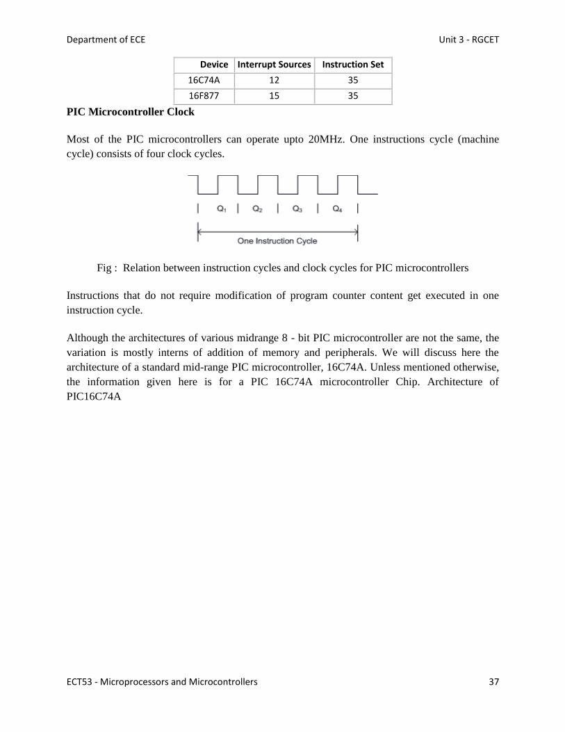
Most of the PIC microcontrollers can operate upto 20MHz. One instructions cycle (machine
cycle) consists of four clock cycles.
Fig : Relation between instruction cycles and clock cycles for PIC microcontrollers
Instructions that do not require modification of program counter content get executed in one
instruction cycle.
Although the architectures of various midrange 8 - bit PIC microcontroller are not the same, the
variation is mostly interns of addition of memory and peripherals. We will discuss here the
architecture of a standard mid-range PIC microcontroller, 16C74A. Unless mentioned otherwise,
the information given here is for a PIC 16C74A microcontroller Chip. Architecture of
PIC16C74A
Department of ECE Unit 3 - RGCET
ECT53 - Microprocessors and Microcontrollers 38
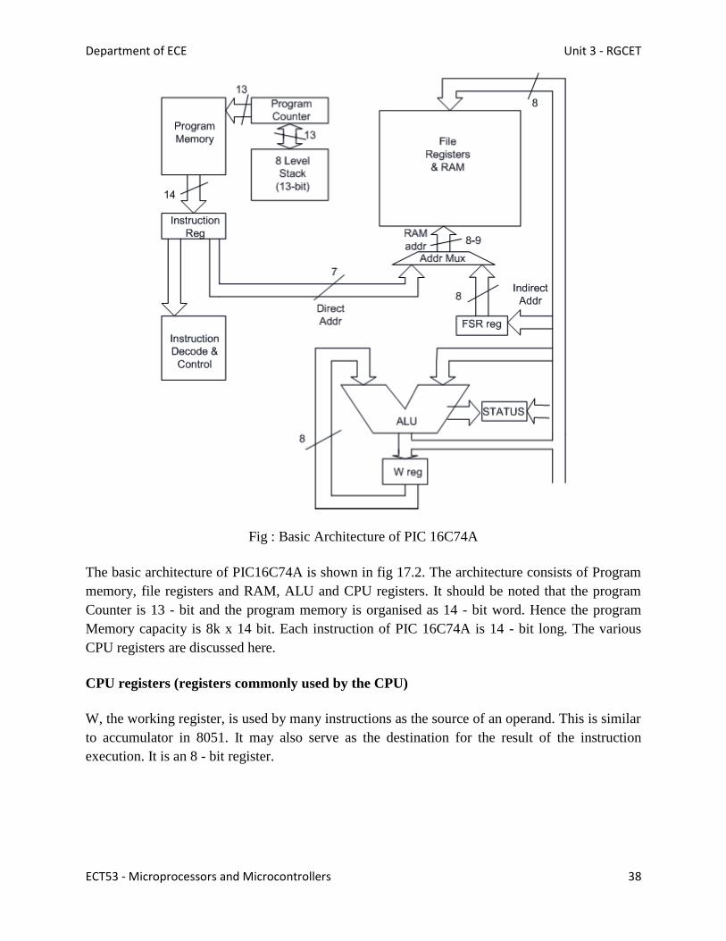
Fig : Basic Architecture of PIC 16C74A
The basic architecture of PIC16C74A is shown in fig 17.2. The architecture consists of Program
memory, file registers and RAM, ALU and CPU registers. It should be noted that the program
Counter is 13 - bit and the program memory is organised as 14 - bit word. Hence the program
Memory capacity is 8k x 14 bit. Each instruction of PIC 16C74A is 14 - bit long. The various
CPU registers are discussed here.
CPU registers (registers commonly used by the CPU)
W, the working register, is used by many instructions as the source of an operand. This is similar
to accumulator in 8051. It may also serve as the destination for the result of the instruction
execution. It is an 8 - bit register.

Department of ECE Unit 3 - RGCET
ECT53 - Microprocessors and Microcontrollers 39
Fig : W register
STATUS Register
The STATUS register is a 8-bit register that stores the status of the processor. This also stores
carry, zero and digit carry bits.
STATUS - address 03H, 83H
Fig : STATUS register
C = Carry bit
DC = Digit carry (same as auxiliary carry)
Z = Zero bit
NOT_TO and NOT_PD - Used in conjunction with PIC's sleep mode
RP0- Register bank select bit used in conjunction with direct addressing mode.
FSR Register (File Selection Register, address = 04H, 84H)
FSR is an 8-bit register used as data memory address pointer. This is used in indirect addressing
mode.
INDF Register (INDirect through FSR, address = 00H, 80H)
INDF is not a physical register. Accessing INDF access is the location pointed to by FSR in
indirect addressing mode.
PCL Register (Program Counter Low Byte, address = 02H, 82H)
PCL is actually the lower 8-bits of the 13-bit program counter. This is a both readable and
writable register.
PCLATH Register (Program Counter Latch, address = 0AH, 8AH)
PCLATH is a 8-bit register which can be used to decide the upper 5bits of the program counter.
PCLATH is not the upper 5bits of the program counter. PCLATH can be read from or written to
without affecting the program counter. The upper 3bits of PCLATH remain zero and they serve
no purpose. When PCL is written to, the lower 5bits of PCLATH are automatically loaded to the
upper 5bits of the program counter, as shown in the figure.

Department of ECE Unit 3 - RGCET
ECT53 - Microprocessors and Microcontrollers 40
Fig : Schematic of how PCL is loaded from PCLATH
Program Counter Stack
An independent 8-level stack is used for the program counter. As the program counter is 13bit,
the stack is organized as 8x13bit registers. When an interrupt occurs, the program counter is
pushed onto the stack. When the interrupt is being serviced, other interrupts remain disabled.
Hence, other 7 registers of the stack can be used for subroutine calls within an interrupt service
routine or within the mainline program.
Register File Map

Department of ECE Unit 3 - RGCET
ECT53 - Microprocessors and Microcontrollers 41
Fig : Register File Map

Department of ECE Unit 3 - RGCET
ECT53 - Microprocessors and Microcontrollers 42
It can be noted that some of the special purpose registers are available both in Bank-0 and Bank-
1. These registers have the same value in both banks. Changing the register content in one bank
automatically changes its content in the other bank.
Port Structure and Pin Configuration of PIC 16C74A
As mentioned earlier, there is a large variety of PIC microcontrollers. However, the midrange
architectures are widely used. Our discussion will mainly confine to PIC16C74A whose
architecture has most of the required features of a mid-range PIC microcontroller. Study of any
other mid-range PIC microcontroller will not cause much variation from the basic architecture of
PIC 16C74A ..
PIC 16C74A has 5 I/O Ports. Each port is a bidirectional I/O port. In addition, they have the
following alternate functions.
In addition to I/O pins, there is a Master clear pin (MCLR) which is equivalent to reset in 8051.
However, unlike 8051, MCLR should be pulled low to reset the micro controller. Since
PIC16C74Ahas inherent power-on reset, no special connection is required with MCLR pin to
reset the micro controller on power-on.
There are two VDD pins and two VSS pins. There are two pins (OSC1 and OSC2) for
connecting the crystal oscillator/ RC oscillator. Hence the total number of pins with a 16C74A is
33+7=40. This IC is commonly available in a dual-in-pin (DIP) package.

Department of ECE Unit 3 - RGCET
ECT53 - Microprocessors and Microcontrollers 43
Fig : Pin configuration of PIC 16C74A
Instruction Set of PIC Microcontroller
Guidelines from Microchip Technology
For writing assembly language program Microchip Technology has suggested the following guidelines.
1. Write instruction mnemonics in lower case. (e.g., movwf) 2. Write the special register names, RAM variable names and bit names in upper case. (e.g., PCL,
RP0, etc.) 3. Write instructions and subroutine labels in mixed case. (e.g., Mainline, LoopTime)
Instruction Set:
The instruction set for PIC16C74A consists of only 35 instructions. Some of these instructions are byte
oriented instructions and some are bit oriented instructions.
The byte oriented instructions that require two parameters (For example, movf f, F(W)) expect the f to
be replaced by the name of a special purpose register (e.g., PORTA) or the name of a RAM variable (e.g.,
NUM1), which serves as the source of the operand. 'f' stands for file register. The F(W) parameter is the
destination of the result of the operation. It should be replaced by:
F, if the destination is to be the source register.
W, if the destination is to be the working register (i.e., Accumulator or W register).

Department of ECE Unit 3 - RGCET
ECT53 - Microprocessors and Microcontrollers 44
The bit oriented instructions also expect parameters (e.g., btfsc f, b). Here 'f' is to be replaced by the
name of a special purpose register or the name of a RAM variable. The 'b' parameter is to be replaced by
a bit number ranging from 0 to 7.
For example:
Z equ 2
btfsc STATUS, Z
Z has been equated to 2. Here, the instruction will test the Z bit of the STATUS register and will skip the
next instruction if Z bit is clear.
The literal instructions require an operand having a known value (e.g., 0AH) or a label that represents a
known value.
For example:
NUM equ 0AH ; Assigns 0AH to the label NUM ( a constant )
movlw NUM ; will move 0AH to the W register.
Every instruction fits in a single 14-bit word. In addition, every instruction also executes in a single cycle,
unless it changes the content of the Program Counter. These features are due to the fact that PIC micro
controller has been designed on the principles of RISC (Reduced Instruction Set Computer) architecture.
Instruction set:
Mnemonics Description Instruction
Cycles
bcf f, b Clear bit b of register f 1
bsf f, b Set bit b of register f 1
clrw Clear working register W 1
clrf f Clear f 1
movlw k Move literal 'k' to W 1
movwf f Move W to f 1
movf f, F(W) Move f to F or W 1
swapf f, F(W) Swap nibbles of f, putting result in F or W 1
andlw k And literal value into W 1
andwf f, F(W) And W with F and put the result in W or F 1
andwf f, F(W) And W with F and put the result in W or F 1
iorlw k inclusive-OR literal value into W 1

Department of ECE Unit 3 - RGCET
ECT53 - Microprocessors and Microcontrollers 45
iorwf f, F(W) inclusive-OR W with f and put the result in F or W 1
xorlw k Exclusive-OR literal value into W 1
xorwf f, F(W) Exclusive-OR W with f and put the result in F or W 1
addlw k Add the literal value to W and store the result in W 1
addwf f, F(W) Add W to f and store the result in F or W 1
sublw k Subtract the literal value from W and store the result in W 1
subwf f, F(W) Subtract f from W and store the result in F or W 1
rlf f, F(W) Copy f into F or W; rotate F or W left through the carry bit 1
rrf f, F(W) Copy f into F or W; rotate F or W right through the carry bit 1
btfsc f, b Test 'b' bit of the register f and skip the next instruction if bit
is clear 1 / 2
btfss f, b Test 'b' bit of the register f and skip the next instruction if bit
is set 1 / 2
decfsz f, F(W) Decrement f and copy the result to F or W; skip the next
instruction if the result is zero 1 / 2
incfcz f, F(W) Increment f and copy the result to F or W; skip the next
instruction if the result is zero 1 / 2
goto label Go to the instruction with the label "label" 2
call label Go to the subroutine "label", push the Program Counter in
the stack 2
retrun Return from the subroutine, POP the Program Counter from
the stack 2
retlw k Retrun from the subroutine, POP the Program Counter from
the stack; put k in W 2
retie Return from Interrupt Service Routine and re-enable
interrupt 2
clrwdt Clear Watch Dog Timer 1
sleep Go into sleep/ stand by mode 1
nop No operation 1
Encoding of instruction:
As has been discussed, each instruction is of 14-bit long. These 14-bits contain both op-code and the
operand. Some examples of instruction encoding are shown here.
Example-1:
bcf f, b Clear 'b' bit of register 'f'

Department of ECE Unit 3 - RGCET
ECT53 - Microprocessors and Microcontrollers 46
Operands: 0 ≤ f ≤ 127
0 ≤ b ≤ 7
Encoding:
The instruction is executed in one instruction cycle, i.e., 4 clock cycles. The activities in various clock
cycles are as follows.
Example-2:
goto K Go to label 'k' instruction
Operand: 0 ≤ K ≤ 2047 (11-bit address is specified) Operation: K PC <10:0>
PCLATH <4:3> PC <12:11> Encoding:
Since this instruction requires modification of program Counter, it takes two instruction cycles for
execution.
Q-Cycle activities are shown as follows.

Department of ECE Unit 3 - RGCET
ECT53 - Microprocessors and Microcontrollers 47
I/O Port Configuration
I/O ports of PIC16C74A:
PIC16C74A has five I/O ports. Port-B, Port-C and Port-D have 8 pins each. Port-A and Port-E have 6 and 3
pins respectively. Each port has bidirectional digital I/O capability. In addition, these I/O ports are
multiplexed with alternate functions for the peripheral devices on the microcontroller. In general, when
a peripheral is enabled, that pin may not be used as a general purpose I/O pin. Each port latch has a
corresponding TRIS (Tri-state Enable) register for configuring the port either as an input or as an output.
The port pins are designated by the alphabet R, followed by the respective port (viz. A, B, C, D or E) and
the pin number. For example, Port-A pins are named as RA0, RA1, etc.
Port-A
Port-A pins RA0-RA3 and RA5 are similar. These pins function (alternate function) as analog inputs to the
analog-to-digital converter.

Department of ECE Unit 3 - RGCET
ECT53 - Microprocessors and Microcontrollers 48
Fig : RA0-RA3 and RA5 pin of Port-A
The structure of Port-A pins RA0-RA3 and RA5 is shown in the figure. TRISA register decides whether the
port-pin is configured as an input or as an output (digital) pin. Setting a TRISA register bit puts the
corresponding output driver in high impedance mode. In this mode, the pin can be used as a digital or
analog input. Clearing a bit in the TRISA register puts the contents of the data latch on the selected pins,
i.e., the pin functions as a digital output. Pins RA0-RA and RA5 have current sourcing capability of 25mA.
The alternate function of RA4 pin is Timer-0 clock input (T0CKI). RA4 pin is an open drain pin and hence
requires external pull-up when configured as output pin. It is shown in the following figure.

Department of ECE Unit 3 - RGCET
ECT53 - Microprocessors and Microcontrollers 49
Fig : RA4 pin Configuration
Configuration of Port-A pins Example : Set RA0-RA3 as outputs and RA4 - RA5 as inputs.
bcf STATUS, RP0 ; Select Bank-0
clrf PORTA ; Clears the data latch
bsf STATUS, RP0 ; Select Bank-1
movlw 30H ; W 03H ( data direction )
movwf TRISA ; Set RA0-RA3 as outputs, RA4-RA5 as inputs
Port-B
Port-B is an 8-bit bidirectional I/O port. The data direction in Port-B is controlled by TRISB register.
Setting a bit in TRISB register puts the corresponding output in high impedance input mode. When a bit
in TRISB is made zero, the corresponding pin in Port-B outputs the content of the latch (output mode).
Each port pin has a weak internal pull-up that can be enabled by clearing bit of OPTION register
(bit-7). When a pin is configured in the output mode, the weak pull-up is automatically turned off.
Internal pull-up is used so that we can directly drive a device from the pins.

Department of ECE Unit 3 - RGCET
ECT53 - Microprocessors and Microcontrollers 50
Fig : Pins RB0-RB3 of Port-B
Configuration of Port-B pins Example : Set RB0-RB3 as outputs, RB4-RB5 as inputs, RB7 as output.
bcf STATUS, RP0
clrf PORTB
bsf STATUS, RP0
movlw 70H
movwf TRISB
Timer modules in PIC Microcontroller
Overview of Timer Modules :
PIC 16C74A has three modules, viz., Timer-0, Timer-1 and Timer-2. Timer-0 and Timer-2 are 8-bit timers.
Timer-1 is a 16-bit timer. Each timer module can generate an interrupt on timer overflow.
Timer-0 Overview:

Department of ECE Unit 3 - RGCET
ECT53 - Microprocessors and Microcontrollers 51
The timer-0 module is a simple 8-bit UP counter. The clock source can be either the internal clock (fosc
/4) or an external clock. When the clock source is external, the Timer-0 module can be programmed to
increment on either the rising or falling clock edge. Timer-0 module has a programmable pre-scaler
option. This pre-scaler can be assigned either to Timer-0 or the Watch dog timer, but not to both.
The Timer-0 Counter sets a flag T0IF (Timer-0 Interrupt Flag) when it overflows and can cause an
interrupt at that time if that interrupt source has been enabled, (T0IE = 1), i.e., timer-0 interrupt enable
bit = 1.
OPTION Register Configuration : Option Register (Addr: 81H) Controls the prescaler and Timer -0 clock
source. The following OPTION register configuration is for clock source = fosc /4 and no Watchdog timer.
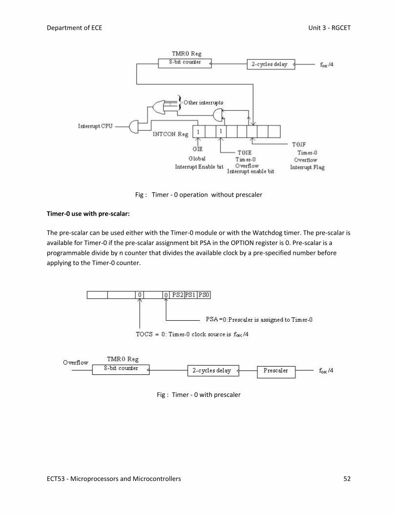
Timer-0 use without pre-scalar
Internal clock source of f osc /4. (External clock source, if selected, can be applied at RA4/TOCKI input at
PORTA).
The following diagram shows the timer use without the prescaler.
Department of ECE Unit 3 - RGCET
ECT53 - Microprocessors and Microcontrollers 52
Fig : Timer - 0 operation without prescaler
Timer-0 use with pre-scalar:
The pre-scalar can be used either with the Timer-0 module or with the Watchdog timer. The pre-scalar is
available for Timer-0 if the pre-scalar assignment bit PSA in the OPTION register is 0. Pre-scalar is a
programmable divide by n counter that divides the available clock by a pre-specified number before
applying to the Timer-0 counter.
Fig : Timer - 0 with prescaler

Department of ECE Unit 3 - RGCET
ECT53 - Microprocessors and Microcontrollers 53
Timer - 1 Module
Timer 1 module is a 16-bit timer/counter consisting of two 8-bit registers (TMR1H and TMR1L) which are
readable and writable. The TMR1 register pair (TMR1H:TMR1L) increments from 0000H to FFFFH and
rolls over to 0000H. The TMR1 interrupt, if enabled, is generated on overflow, which sets the interrupt
flag bit TMR1IF (bit-0 of PIR1 register). This interrupt can be enabled/disabled by setting/clearing TMR1
interrupt enable bit TMR1IE (bit-0 of the PIE1 register).
The operating and control modes of Timer1 are determined by the special purpose register T1CON.
Various bits of T1CON register are given as follows:-
Fig : T1CON Register
TMR1 ON : Timer1 ON bit
0 = stops Timer 1; 1 = Enables Timer 1 TMR1CS : Timer 1 Clock source Select Bit
1 = External Clock (RCO/T1OSO/T1CKI)
0 = Internal Clock ( ) : Timer 1 External Clock Input Synchronization Bit
(Valid if TMR1CS = 1)
1 - Do not synchronize
0 - Synchronize

Department of ECE Unit 3 - RGCET
ECT53 - Microprocessors and Microcontrollers 54
T1OSCEN: Oscillator enable control bit
1 = Oscillator is enabled
0 = Oscillator is shut off
Timer 1 Input Clock Prescaler
Select bits Prescaler Value
T1CKPS1 T1CKPS0
1 1 1:8
1 0 1:4
0 1 1:2
0 0 1:1
Fig : Operation of Timer 1
Timer 1 can operate in one of the two modes
As a timer (TMR1CS = 0). In the timer mode, Timer 1 increments in every instruction cycle. The
timer 1 clock source is . Since the internal clock is selected, the timer is always synchronized and there is no further need of synchronization.
As a counter (TMR1CS = 1). In the counter mode, external clock input from the pin RCO/T1CKI is selected.
Reading and writing Timer 1

Department of ECE Unit 3 - RGCET
ECT53 - Microprocessors and Microcontrollers 55
Reading TMR1H and TMR1L from Timer 1, when it is running from an external clock source, have to be
done with care. Reading TMR1H or TMR1L for independent 8 - bit values does not pose any problem.
When the 16-bit value of the Timer is required, the high byte (TMR1H) is read first followed by the low
byte (THR1lL). It should be ensured that TMR1L does not overflow (that is goes from FFH to 00H) since
THR1H was read. This condition is verified by reading TMR1H once again and comparing with previous
value of TMR1H.
Example Program
Reading 16bit of free running Timer 1
movf TMR1H ; read high byte
movwf TMPH ; store in TMPH
movf TMR1L ; read low byte
movwf TMPL ; store in TMPL
movf TMR1H, W ; read high byte in W
subwf TMPH, W ; subtract 1 st read with 2 nd read
btfsc STATUS, Z ; and check for equality
goto next ;
; if the high bytes differ, then there is an overflow
; read the high byte again followed by the low byte
movf TMR1H, W ; read high byte
movwf TMPH
movf TMR1L, W ; read low byte
movwf TMPL
next : nop

Department of ECE Unit 3 - RGCET
ECT53 - Microprocessors and Microcontrollers 56
Timer 2 Overview
Fig : Schematic diagram showing operation of Timer 2
Timer 2 is an 8 - bit timer with a pre-scaler and a post-scaler. It can be used as the PWM time base for
PWM mode of capture compare PWM (CCP) modules. The TMR2 register is readable and writable and is
cleared on device reset.
The input clock ( ) has a pre-scaler option of 1:1, 1:4 or 1:16 which is selected by bit 0 and bit 1 of
T2CON register respectively.
The Timer 2 module has an 8bit period register (PR2). Timer-2 increments from 00H until it is equal to
PR2 and then resets to 00H on the next clock cycle. PR2 is a readable and writable register. PR2 is
initailised to FFH on reset.
The output of TMR2 goes through a 4bit post-scaler (1:1, 1:2, to 1:16) to generate a TMR2 interrupt by
setting TMR2IF.

Department of ECE Unit 3 - RGCET
ECT53 - Microprocessors and Microcontrollers 57
Fig : The T2CON Register
Interrupt Logic in PIC 16C74A
PIC 16C74A microcontroller has one vectored interrupt location (i.e., 0004H) but has 12 interrupt
sources. There is no interrupt priority. Only one interrupt is served at a time. However interrupts can be
masked. The interrupt logic is shown below :

Department of ECE Unit 3 - RGCET
ECT53 - Microprocessors and Microcontrollers 58
Fig : Schematic diagram showing the interrupt logic for PIC
CCP Modules
Capture / Compare /PWM (CCP) Modules:
PIC16C74A has two CCP Modules. Each CCP module contains a 16 bit register (two 8-bit registers) and
can operate in one of the three modes, viz., 16-bit capture, 16-bit compare, or up to 10-bit Pulse Width
Modulation (PWM). The details of the two modules (CCP1 and CCp2) are given as follows.
CCP1 Module:
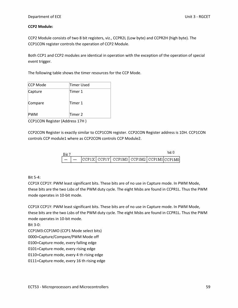
CCP1 Module consists of two 8-bit registers, viz., CCPR1L (low byte) and CCPR1H (high byte). The
CCP1CON register controls the operation of CCP1 Module.
Department of ECE Unit 3 - RGCET
ECT53 - Microprocessors and Microcontrollers 59
CCP2 Module:
CCP2 Module consists of two 8 bit registers, viz., CCPR2L (Low byte) and CCPR2H (high byte). The
CCP1CON register controls the operation of CCP2 Module.
Both CCP1 and CCP2 modules are identical in operation with the exception of the operation of special
event trigger.
The following table shows the timer resources for the CCP Mode.
CCP Mode Timer Used
Capture
Compare
PWM
Timer 1
Timer 1
Timer 2
CCP1CON Register (Address 17H )
CCP2CON Register is exactly similar to CCP1CON register. CCP2CON Register address is 1DH. CCP1CON
controls CCP module1 where as CCP2CON controls CCP Module2.
Bit 5-4:
CCP1X CCP1Y: PWM least significant bits. These bits are of no use in Capture mode. In PWM Mode,
these bits are the two Lsbs of the PWM duty cycle. The eight Msbs are found in CCPR1L. Thus the PWM
mode operates in 10-bit mode.
CCP1X CCP1Y: PWM least significant bits. These bits are of no use in Capture mode. In PWM Mode,
these bits are the two Lsbs of the PWM duty cycle. The eight Msbs are found in CCPR1L. Thus the PWM
mode operates in 10-bit mode.
Bit 3-0:
CCP1M3:CCP1MO (CCP1 Mode select bits)
0000=Capture/Compare/PWM Mode off
0100=Capture mode, every falling edge
0101=Capture mode, every rising edge
0110=Capture mode, every 4 th rising edge
0111=Capture mode, every 16 th rising edge

Department of ECE Unit 3 - RGCET
ECT53 - Microprocessors and Microcontrollers 60
1000=Compare mode, set output on match (CCP1IF bit is set)
1001=Compare mode, clear output on match (CCP1IF bit is set)
1010=Compare mode, generate software interrupt on match (CCP1IF bit is set, CCP1 pin unaffected)
1011=Compare mode, trigger special event (CCP1IF bit is set;CCP1 resets Tmr1; CCP2 resets TMR1 and
starts A/D conversion if A/D module is Enabled)
11XX=PWM mode.
Capture Mode (CCP1):
Capture Mode captures the 16-bit value of TMR1 into CCPR1H:CCPR1L register pair in response to an
event occurring on RC2/CCP1 pin. Capture Mode for CCP2 is exactly similar to that of CCP1.
An event on RC2/CCP1 pin is defined as follows:
Every falling edge Every rising edge. Every 4 th rising edge. Every 16 th rising edge.
As mentioned earlier, this event is decided by bit 3-0 of CCP1CON register.
Schematic diagram for capture mode of operation
Fig : Capture operation
Required condition for capture mode:
1. RC2/CCP1 pin should be configured as an input by setting TRISC (bit 2). 2. Timer 1 should be operated from the internal clock (fosc/4), i.e., timer mode or in synchronized
counter mode.
Compare Mode (CCP1)

Department of ECE Unit 3 - RGCET
ECT53 - Microprocessors and Microcontrollers 61
Compare mode for CCP2 is similar to that of CCP1, except that in special event trigger mode, CCP1 resets
TMR1 only, whereas CCP2 resets TMR1 and starts A/D conversion if A/D module is enabled.
In compare mode, the 16-bit CCPR1 register value is compared against TMR1 register pair (TMR1H and
TMR1L) value. When a match occurs, the RC2/CCP1 pin is driven high or driven low or remains
unchanged as decided by CCP1CON<3:0> bits.
Fig : Compare Operation
Required conditions for compare mode
1. RC2/CCP1 pin must be configured as an output by clearing TRISC<2> bit. 2. Timer-1 should be operated in timer mode (i.e., internal clock source of fosc/4) or in
synchronized counter mode.
In software interrupt mode, CCP1IF bit is set but CCP1 pin in unaffected. As shown in the figure, in
special event trigger mode, both CCP1 and CCP2 intiates an A/D conversion. PWM mode (CCP1) Both
CCP1 and CCP2 have similar operation in PWM mode. Here we will discuss PWM with respect to CCP1.
In PWM mode, the CCP1 pin produces upto a 10-bit resolution Pulse Width Modulation (PWM) output.
RC2/CCP1 pin should be configured in the uotput mode by clearing TRISC<2> bit.
The schematic block diagram of CCP1 module in PWM mode is shown in the figure.

Department of ECE Unit 3 - RGCET
ECT53 - Microprocessors and Microcontrollers 62
Fig : PWM Operation
It can be noted that PR2 (Period Register, 8 bit) decides the PWM period where CCPR1L (8-bits) and
CCP1CON <5:4> (2-bits) decide the PWM duty cycle. When TMR2 equals PR2, the SR latch is set and
RC2/CCP1 pin is pulled high. In the same time, TMR2 is cleared and the duty cycle value available in
CCPR1L is latched to CCPR1H. CCPR1H, CCP1CON <5:4> decide the duty cycle and when this 10-bit
ewquals the TMR2+2 prescaler or Q-bits, the SR latch is set and RC2/CCP1 pin is driven low.
A PWM output as shown has a time period. The time for which the output stays high is called duty cycle.
PWM Period

Department of ECE Unit 3 - RGCET
ECT53 - Microprocessors and Microcontrollers 63
The PWM period is specified by writing to PR2 register. The PWM period can be calculated using the
following formula:
PWM period = [( PR 2) + 1] × 4 × T osc × (TMR2 prescale value)
PWM frequency = 1/ PWM period
When TMR2 is equal to PR2, the following events occur on the next increment cycle.
TMR2 is cleared the CCP1 pin is set (if PWM duty cycle is 0 The PWM duty cycle is latched from CCPR1L into CCPR1H
PWM duty cycle
The PWM duty cycle is specified by writing to the CCPR1L register and to CCP1CON < 5 : 4 >
bits. Up to 10-bit resolution is available where CCPR1L contains the eight MSBs and CCP1CON < 5 : 4 >
contains the two LSB's. The 10-bit value is represented by CCPR1L : CCP1CON < 5 : 4 >.
The PWM duty cycle is given by
PWM duty cycle = (CCPR1L : CCP1CON < 5 : 4 > ). T osc . (TMR2 prescale value)
To understand the 10-bit counter configuration from Timer-2, let us first see the counting mechanism of
Timer-2, as shown in Fig 22.4.
Fig : Counting mechanism in Timer - 2
If the prescaler is 1, the 10-bit counter is configured as follows
Fig : Prescaler set to divide by one

Department of ECE Unit 3 - RGCET
ECT53 - Microprocessors and Microcontrollers 64
If the prescaler is 4, the 10-bit counter is configured as follows.
Fig : Prescaler programed to divide by four
If the prescaler is 16, the 10-bit counter is realized as follows.
Fig : Prescaler programed to divide by 16
Although CCPR1L and CCP1CON < 5 : 4 > can be written to at anytime, the duty cycle value is not latched
into CCPR1H until a match between PR2 and TMR2 occurs. In PWM mode, CCPR1H is a read-only
register.
The CCPR1H register and a 2-bit internal latch are used to double buffer the PWM duty cycle. This
double buffering is essential for glitchless PWM operation. When the CCPR1H and 2-bit latch match
TMR2 concatenated with an internal 2-bit Q clock or 2-bits of prescaler, the CCP1 pin is cleared.
Maximum PWM resolution (bits) for a given PWM frequency can be calculated as
If the PWM duty cycle is longer than the PWM period, then the CCP1 pin will not be cleared.
PWM Period and duty cycle calculation
Example:
Desired PWM frequency = 78.125 kHz
f osc = 20MHz
TMR2 Prescalar = 1

Department of ECE Unit 3 - RGCET
ECT53 - Microprocessors and Microcontrollers 65
Find the maximum resolution of duty cycle that can be used with a 78.124 kHz frequency and 20 MHz
oscillator.
256 = 2PWM Resolution
At most, an 8-bit resolution duty cycle can be obtained from a 78.125 kHz frequency and 20 MHz
oscillator
ie, 0 CCPR1L : CCP1CON <5 : 4> ≤ 255 .
Any value greater than 255 will result in a 100 % duty cycle. The following table gives the PWM
frequency fPWM if fosc = 20MHz
Duty cycle resolution 10-Bit counter scale PR2 value Prescaler 1 Prescaler 4 Prescaler 16
10 bit 1024 255 19.53 KHz 4.88 kHz 1.22 kHz
≈ 10 bit 1000 249 20kHz 5kHz 1.25kHz
8 bit 256 63 78.125kHz 19.53kHz 4.88kHz
6 bit 64 15 312.5kHz 78.125kHz 19.53kHz
ARM PROCESSOR
INTRODUCTION
ARM, originally Acorn RISC Machine, later Advanced RISC Machine, is a family
of reduced instruction set computing (RISC) architectures for computer processors,
configured for various environments.

Department of ECE Unit 3 - RGCET
ECT53 - Microprocessors and Microcontrollers 66
A RISC-based computer design approach means processors require
fewer transistors than typical complex instruction set computing (CISC) x86 processors in
most personal computers.
This approach reduces costs, heat and power use. Such reductions are desirable traits for
light, portable, battery-powered devices including smart phones, laptops, tablet and notepad
computers, and other embedded systems.
A BRIEF HISTORY
ARM was formed in 1990 as Advanced RISC Machines Ltd., a joint venture of Apple
Computer, Acorn Computer Group, and VLSI Technology.
In 1991, ARM introduced the ARM6 processor family, and VLSI became the initial
licensee. Subsequently, additional companies, including Texas Instruments, NEC, Sharp,
and ST Microelectronics, licensed the ARM processor designs, extending the applications
of ARM processors into mobile phones, computer hard disks, personal digital assistants
(PDAs), home entertainment systems, and many other consumer products.
Nowadays, ARM partners ship in excess of 2 billion ARM processors each year.
Unlike many semiconductor companies, ARM does not manufacture processors or sell the
chips directly.
Instead, ARM licenses the processor designs to business partners, including a
majority of the world’s leading semiconductor companies. Based on the ARM low-cost
and power-efficient processor designs, these partners create their processors,
microcontrollers, and system-on-chip solutions. This business model is commonly called
intellectual property (IP) licensing. In addition to processor designs, ARM also licenses
systems-level IP and various software IPs.
To support these products, ARM has developed a strong base of development tools,
hardware, and software products to enable partners to develop their own products.
FEATURES OF THE ARM PROCESSOR
• Incorporate features of Berkeley RISC design -a large register file -a load/store
architecture -uniform and fixed length instruction field -simple addressing mode
• Other ARM architecture features -Arithmetic Logic Unit and barrel shifter -auto
increment and decrement addressing mode -conditional execution of instructions
• Based on Von Neumaan Architecture or Harvard Architecture.
INTERNAL ARCHITECTURE OF ARM PROCESSOR

Department of ECE Unit 3 - RGCET
ECT53 - Microprocessors and Microcontrollers 67
PIPELINE STAGES
the two Fetch stages
a Decode stage
an Issue stage
the four stages of the MP11 CPU integer execution pipeline.
These eight stages make up the MP11 CPU pipeline.
The pipeline stages are:
Fe1

Department of ECE Unit 3 - RGCET
ECT53 - Microprocessors and Microcontrollers 68
First stage of instruction fetch and branch prediction.
Fe2
Second stage of instruction fetch and branch prediction.
De
Instruction decode.
Iss
Register read and instruction issue.
Sh
Shifter stage.
ALU
Main integer operation calculation.
Sat
Pipeline stage to enable saturation of integer results.
WBex
Write back of data from the multiply or main execution pipelines.
MAC1
First stage of the multiply-accumulate pipeline.
MAC2
Second stage of the multiply-accumulate pipeline.
MAC3
Third stage of the multiply-accumulate pipeline.
ADD
Address generation stage.
DC1
First stage of Data Cache access.
DC2
Second stage of Data Cache access.
WBls
Write back of data from the Load Store Unit.
Department of ECE Unit 3 - RGCET
ECT53 - Microprocessors and Microcontrollers 69
By overlapping the various stages of operation, the MP11 CPU maximizes the clock rate
achievable to execute each instruction. It delivers a throughput approaching one instruction for
each cycle.
The Fetch stages can hold up to four instructions, where branch prediction is performed on
instructions ahead of execution of earlier instructions.
The Issue and Decode stages can contain any instruction in parallel with a predicted branch.
The Execute, Memory, and Write stages can contain a predicted branch, an ALU or multiply
instruction, a load/store multiple instruction, and a coprocessor instruction in parallel execution.
OPERATING MODES
The ARM7TDMI processor has seven modes of operation:
User mode is the usual ARM program execution state, and is used for executing most
application programs.
Fast Interrupt (FIQ) mode supports a data transfer or channel process.
Interrupt (IRQ) mode is used for general-purpose interrupt handling.
Supervisor mode is a protected mode for the operating system.
Abort mode is entered after a data or instruction Prefetch Abort.
System mode is a privileged user mode for the operating system.
Undefined mode is entered when an undefined instruction is executed.
Modes other than User mode are collectively known as privileged modes. Privileged modes are
used to service interrupts or exceptions, or to access protected resources.
PROCESSOR CORE REGISTER
The processor has the following 32-bit registers:
13 general-purpose registers, r0-r12
Stack Pointer (SP) alias of banked registers, SP_process and SP_main
Link Register (LR), r14
Program Counter (PC), r15
Special-purpose Program Status Registers, (xPSR).
The general-purpose registers r0-r12 have no special architecturally-defined uses. Most
instructions that can specify a general-purpose register can specify r0-r12.
Low registers
Registers r0-r7 are accessible by all instructions that specify a general-purpose register.
High registers

Department of ECE Unit 3 - RGCET
ECT53 - Microprocessors and Microcontrollers 70
Registers r8-r12 are accessible by all 32-bit instructions that specify a general-purpose
register.
Registers r8-r12 are not accessible by all 16-bit instructions.
Registers r13, r14, and r15 have the following special functions:
Stack pointer
Register r13 is used as the Stack Pointer (SP). Because the SP ignores writes to bits [1:0],
it is autoaligned to a word, four-byte boundary.
Handler mode always uses SP_main, but you can configure Thread mode to use either
SP_main or SP_process.
Link register
Register r14 is the subroutine Link Register (LR).
The LR receives the return address from PC when a Branch and Link (BL) or Branch and
Link with Exchange (BLX) instruction is executed.
The LR is also used for exception return.
At all other times, you can treat r14 as a general-purpose register.
Program counter
Register r15 is the Program Counter (PC).
Bit [0] is always 0, so instructions are always aligned to word or halfword boundaries.
See the ARMv7-M Architecture Reference Manual for more information.