unclassified ad number limitation changes ad number limitation changes to: from: ... semiconductor...
TRANSCRIPT

UNCLASSIFIED
AD NUMBER
LIMITATION CHANGESTO:
FROM:
AUTHORITY
THIS PAGE IS UNCLASSIFIED
AD813109
Approved for public release; distribution isunlimited.
Distribution authorized to U.S. Gov't. agenciesand their contractors; Critical Technology; APR1967. Other requests shall be referred to ArmyElectronics Command, ATTN: AMSEL-KL-SM, FortMonmouth, NJ 07703-5601. This document containsexport-controlled technical data.
ECOM ltr dtd 30 Jul 1971

t
© r-( CO
00
AD
Technical Report ECOM—01660-6
MICROWAVE OSCILLATIONS IN BULK SEMICONDUCTORS
Sixth Quarterly Progress Report
ey
N.BRASLAU, J.M.WOODALL, AND C.LANZA
April 1967
D D C
Sk m 41967
B
ECOM UNITED STATES ARMY ELECTRONICS COMMAND- FORT MONMOUTH. N.J.
CONTRACT DA 28-043 AMC-01550(E)
INTERNATIONAL BUSINESS MACHINES CORP. Thomas J. Watson Research Center Yorktown Heights, N. Y.
This document is subject to special export controls and each transmittai to foreign gov- ernments or foreign nationals may be made only with prior approval of Commanding General, U. S. Army Electronics Command, Fort Monmouth, New Jersey, AMSEL-KL-SM.

DISCLAIMERS
The findings in this report are not to be construed as an official Department of the Army position, unless so designated by other authorized documents.
The citation of trade names and names of manufacturers in this report is not to be construed as official Government Indorse- ment or approval of commercial products or services referenced herein.
DISPOSITION
Destroy this report when It Is no longer needed. Do not return It to the originator. *■
Technical Report ECOM-01550-6 April 1967
MICROWAVE OSCILLATIONS IN BULK SEMICONDUCTORS
SIXTH QUARTERLY PROGRESS REPORT
1 October 1966 to 31 December 1966
REPORT NO. 6
CONTRACT NO. DA-28-043 AMC-01550(E)
"The work prepared under this contract is a part of PROJECT DEFENDER and was made possible by the support of the Advanced Research Projects Agency under Order Number 692, through the U. S, Army Electronics Command. "
Prepared by
N. BRAS LAU, J. M. WOODALL AND C. LANZA
INTERNATIONAL BUSINESS MACHINES CORPORATION THOMAS J. WATSON RESEARCH CENTER
YORKTOWN HEIGHTS, NEW YORK
For
U. S. ARMY ELECTRONICS COMMAND, FORT MONMOUTH, N.J.
"This document is subject to special export controls and each transtnltta! to foreign governments or foreign nationals may be made only with prior approval of Commanding General, U. S. Army Electronics Command, Fort Monmouth, New Jersey, AMSEL-KL-SM. "
..—■■——.„■«,——,—..—.
TABLE OF CONTENTS
Page
Purpose j
Abstract ii
I. Materials Studies i
Tl. Device Studies 4
III. Determination of Drift Velocity 8 as a Function of Field in GaAs
Conclusion 9
References 10
Figure Captions 11
PURPOSE
The purpose of this contract is to Improve the under- standing of current instabllitle« in bulk semiconductors known as the "Gunn Effect" and to investigate the properties of devices employing this phenomenon in order to facilitate an evaluation of their potential as practical microwave circuit elements.
Since this effect depends on the bulk properties of the semiconductor on a microscopic scale, part of this effort will be devoted to the growing and cKaracteriaing of high quality intermediate resistivity (1-100 ohm cm) GaAs, either by the controlled addition of dopants or by the annealing of high re- sistivity material. If the required resistivity can be achieved only by deliberate compensation of donors and acceptors, the problem of obtaining such a balance homogeneously in the material will be investigated.
Although there is now firm evidence that the Gunn effect is a result of intervalley transfer of conduction electrons, a detailed understanding of the mechanism of the instability Is not yet available. One approach will be to study the observed "shock waves" of electric field In the bulk of oscillating sam- ples and to explore the effect of material characteristics, applied electric field, and external circuit parameters on Its behavior and on the output characteristics of the sample.
Another approach will be to perform diagnostic experi- ments on oscillating devices In order to understand their per- formance characteristics and limitations and to determine the underlying causes.

ABSTRACT
The drift velocity as a function of field for heat treated bulk GaAs has been measured by a technique of microwave heating. The results agree with those obtained by Gunn and Elliott using fast pulse techniques and differ significantly from that predicted by the transferred electron model. It has been found that the GaAs melt can leach impurities from the silica envelope surrounding the growth vessel as well as from the vessel itself. When an all Spectrosil system is employed, the heat treatable acceptor present in crystals grown in silica sys- tems appears to be absent. Calculations and experiments showing the adverse effect of temperature rise on oscillators are given.
li
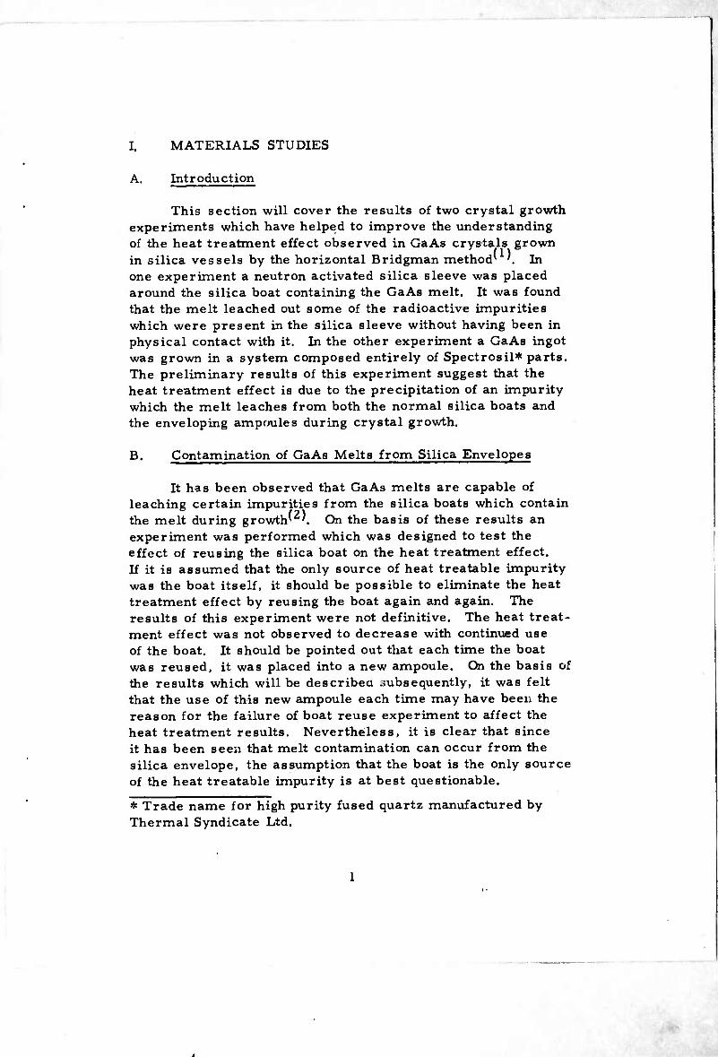
I. MATERIALS STUDIES
A. Introduction
This section will cover the results of two crystal growth experiments which have helped to improve the understanding of the heat treatment effect observed in GaAs crystals grown
ill in silica vessels by the horizontal Bridgman methodv '. In one experiment a neutron activated silica sleeve was placed around the silica boat containing the GaAs melt. It was found that the melt leached out some of the radioactive impurities which were present in the silica sleeve without having been in physical contact with it. In the other experiment a GaAs ingot was grown in a system composed entirely of Spectrosil* parts. The preliminary results of this experiment suggest that the heat treatment effect is due to the precipitation of an impurity which the melt leaches from both the normal silica boats and the enveloping ampoules during crystal growth.
B. Contamination of GaAs Melts from Silica Envelopes
It has been observed that GaAs melts are capable of leaching certain impurities from the silica boats which contain the melt during growth' '. On the basis of these results an experiment was performed which was designed to test the effect of reusing the silica boat on the heat treatment effect. If it is assumed that the only source of heat treatable impurity was the boat itself, it should be possible to eliminate the heat treatment effect by reusing the boat again and again. The results of this experiment were not definitive. The heat treat- ment effect was not observed to decrease with continued use of the boat. It should be pointed out that each time the boat was reused, it was placed into a new ampoule. On the basis of the results which will be described subsequently, it was felt that the use of this new ampoule each time may have been the reason for the failure of boat reuse experiment to affect the heat treatment results. Nevertheless, it is clear that since it has been seen that melt contamination can occur from the silica envelope, the assumption that the boat is the only source of the heat treatable impurity is at best questionable.
* Trade name for high purity fused quartz manufactured by Thermal Syndicate Ltd.

The experiment which invalidated this assumption was performed in the following manner. A 5. 5" x 1. 0" I. D. piece of G. E. type 204 tubing was neutron activated for 288 hours at a flux of 2, 2 x 1013 cm-2 sec"1. After a decay to safe handling level, itwas used for the crystal growth experiment. The melt and sleeve were exposed to each other at about 1250 C for about 16 hours after which time the crystal was grown. The crystal was sectioned at various positions along the axis and measured for pickup of radioactive impurities. Zn, Cr, and Fe are the major impurities which have been identified to date. Quantitatively, it appears as though 1-2 x 10¹⁴ atoms cm"3 of Zn were leached by the melt and were segregated to the first to freeze portion of the crystal. The sleeve was subsequently reused and the resulting crystal was found to contain about an order of magnitude fewer radio- active impurities than the first one. It was concluded that in order to perform meaningful leaching experiments in the future, not only the boat but all the silica parts exposed to high temperatures must be reused also. This feature has been incorporated into experiments which are currently in progress.
C. Growth Using A Spectrosil System
The most interesting experiment which has been performed recently is the one in which the entire glass system used for the GaAs melt and enclosure was composed of Spectrosil. Previously, crystals had been grown using only Spectrosil boats. These crystals also exhibited the heat treat- ment effect. However, in view of the above results(Paragraph B), using Spectrosil boats in type 204 quartz ampoules could not be considered a definitive experiment. One of the major difficulties encountered when using Spectrosil ampoules is that the softening temperature for Spectrosil seems to be somewhat lower than that for G, E. 204 quartz. This is quite a problem for GaAs crystal growth since the melting point for GaAs is quite near the softening point for 204 quartz. When an attempt was made to use a Spectrosil ampoule and boat to grow a GaAs crystal, it was found that the ampoule would either expand or collapse, depending on the As pressure over the melt. This problem was solved by placing a slightly larger 204 support tube over the sealed Spectrosil system. By adjusting the As pressure to cause expansion, the spectro- sil would push out to the supporting 204 tube. A reasonable
analogy would be to imagine an inner tube of a pneumatic tire to be the Spectrosil and the tire to be the 204 support tube. Another major difficulty of using Spectrosil boats is that Spectrosil contains water an an impurity. While this water may not affect the purity of GaAs, it does contribute to the wetting of the boat by the GaAs melt, thereby causing the formation of polycrystalline ingots rather than single crystals. This wetting also induces straining of the ingot during cooling, causing it to fracture into small useless pieces. In spite of these major difficulties, the experiment was highly successful in gaining information about the heat treatment effect. The two results obtained so far are:
1) the crystal had an electron concentration of 2 - 4 x 10 atoms/cc from first-to-freeze position to the last-to-freeze position in the as grown condition,
2) after a 750 C heat treatment, the carrier concentration remained the same.
These preliminary results suggest that the heat treatable acceptor observed in previous material is either not present or at least greatly deminished in the crystal grown in the Spectrosil system. Before anything can definitely be con- cluded, this experiment will have to be repeated under a variety of conditions. However, the evidence so far is that the heat treatable acceptor is a chemical impurity whose major source is the 204 silica crystal growth system.
II. DEVICE STUDIES
A. Effect of Temperature on Efficiency
In order to obtain an indication of temperature effects on the efficiency of oscillation, the average efficiency was measured for various pulse widths, adjusting the repetition frequency to maintain a constant duty cycle of 1%. The average input power under these conditions was about 50 mw. Figure 1 is a plot of the result of this test which shows about an order of magnitude decrease in efficiency (averaged over the pulse width) for pulse widths from 0. 1 to 14|x sec. The efficiency at the end of the pulse is, of course, somewhat lower than the average value.
Another test was made using a constant pulse width of 1 fxs and 1% duty cycle. The coaxial device holder was placed in an oven and the efficiency measured as a function of ambient temperature. Figure 2 shows the result of this test for three units. Two of the devices were made from boat-grown GaAs and one used an epitaxial n layer on a^semi-insulating sub- strate. The normalized curves show that efficiency decreases an order of magnitude at temperatures below 225 C. The spread in the curves may be due to variables In crystal perfection.
Similar tests also show the importance of the tempera- ture rise. For units that would operate cw, it was found that the average power output was about 5 times higher when operated pulsewise at a 20% duty cycle than when operated cw. Since experiments show that the temperature rise should be kept as low as possible to maintain efficiency, careful attention to heat dissipation is essential. Moderate temperatures may be maintained by improved mounting and packaging design, and possibly by the use of geometries which allow the attain- ment of the critical field with a lower input power.
B. Temperature Rise Calculations
In order to estimate the temperature rise associated with the establishment of the critical field, a first-order calculation was made for four different geometries. In this calculation it was assumed that:

a. The thermal conductance (k) is constant with temperature changes,
b. An ideal thermal contact exists between the GaAs and the heat sink,
c. The thermal spreading resistance in the heat sink is negligible, and
d. The heat flows only to the heat sink through the semiconductor (one dimension).
The result of this calculation is shown in Table I. Note that for the above assumptions, the temperature rise is inde- pendent of the semiconductor cross-section area. Included in the table are numerical results for typical values for the four cases. The calculations show that devices made from bulk materiel suffer from the practical aspect of making the active length of the sample small. For the epitaxial layers, either on n or semi-insulating substrates, both the epitaxial layer and the substrate thickness are important. An advantage of the first three geometries is the ease with which a double- ended heat sink can be employed. A small advantage of the ring-dot geometry (described in the 3rd and 4th quarterly reports) is that the input power density varies with radius as 1/r . This allows some heat flow radially in the epitaxial layer, subject to thermal spreading resistance.
It should be pointed out that the results of Table I give lower values for the temperature rise than for actual operation since:
a. The thermal conductivity actually decreases about a factor of 2 for a temperature rise of 100oC.
b. Some thermal spreading resistance does exist in the heat sink, and
c. The thermal contact between the semiconductor and the heat sink is far from ideal.
It is well known that when most semiconductors, and GaAs in

particular, are alloyed with impurities, a significant reduction in the thermal conductivity results. This creates a thermal barrier at the heat sink interface. Experiments indicate that this latter factor may be the more significant one. Chips made of n /n/n layers were made such that the thickness of one n layer was about 3 times that of the other n+ layer. Some Gunn devices are made by alloying the thin n+ layer to a gold-plated copper heat sink, and others were made alloying the thicker layer to the heat sink. They were tested using pulses at a low duty cycle. It was found that the voltage-current waveform showed no significant difference due to the substrate thickness as the pulses were widened until thermal effects were noticeable. This is interpreted to indicate that the alloyed interface is more effective in blocking heat flow than the thermal conductivity of the semiconductor. Essentially the same results were obtained for mounts varying from pill packages to copper blocks.
C. Device Results
Table II is a summary of the devices which successfully operated cw during this period. The table indicates the material type, geometry, and electrical characteristics together with the power output, frequency, and efficiency. Note that our maximum power output in this group was 7. 2 mw with an efficiency of about 1%. This unit was made by vapor growing n+ contact onto a n/n+ slice purchased from Texas Instruments Co. However, this was the only cw device obtained from this batch for about 50 devices. Some ring-dot devices were made to operate cw as shown, one unit producing 5 mw of power.
Table III is a similar compilation for units that were operated in a pulsed mode. The power output represents the maximum average power obtainable by adjusting pulse width, duty cycle, and input pulse amplitude.
D. Device Characteristics
It was observed for the ring-dot geometry made on semi- insulating substrates, that for a cathode radius of 25\i, the Gunn threshold voltage was from 20 to 25 v instead of 12 v . calculated. A possible explanation for this is as follows:

•
Adjacent to the inner electrode radius the Input power density- is maximum so that the maximum temperature rise occurs there. If this temperature rise is sufficient to reduce the lower valley mobility of electrons, the negative resistance be- comes of proper magnitude to start a dipole domain only at a slightly larger radius, where the temperature is somewhat lower. This makes the radius of the inner electrode effectively larger and a higher applied voltage is required for oscillations to begin.
Another interesting effect was observed for the ring-dot structure. After the device was formed and mounted, attempts were made to make the epitaxial n layer between electrodes thinner by etching. This should reduce the input power required to achieve the critical field. It was found, however, that de- vices which oscillated before etching could not be made to oscillate after etching. It is felt that when the device is etched, the n epitaxial layer takes the shape shown in Fig. 3. Most of the applied voltage now drops across the narrow neck formed under the central dot. This neck is so short that the nl product is less than 1012, and the field generated in this region forms a stable domain.
In summary, experiments show that device heating causes a significant decrease in efficiency of oscillations. A simple calculation indicates that for cw operation, temperature rises are expected which will cause the devices to operate in the low efficiency region. Double-ended heat sinks may be necessary to help restrict the temperature rise to tolerable values.

III. DETERMINATION OF DRIFT VELOCITY AS A FUNlCTION. OF FIELD IN GaAs
Because of the disagreement between various measure- ments of the drift velocity as a function of applied electric field in n-type GaAs l3>4' 5' 6.7)i and particularly because of the disagreement between Gunn and Elliott's measurement^ ' with the prediction band on the transferred electron model»°'. it was decided to make this determination by some other independent means.
We have been able to infer this relationship from the measurement of the dc conductivity of a GaAs post subjected to a microwave field with peak values up to sever"1 KV/cm. The result agrees within experimental uncertainl i that calculated from the curve of Gunn and Elliott(3); b ,n the post and Gunn's sample were fabricated from the same crystal of heat treated bulk material of the kind described in previous progress reports. Measurements made at both 9 and 35 GHz gave the same results within experimental uncertainty. The electric field was above threshold for approximately 40 and 10 picoseconds, respectively during each half cycle of the rf field; in both cases this is short compared to the expected domain build-up time. Details of this work will be published in the near future.
It is a bit early to speculate as to the meaning of these results. The first thing to be done is to repeat the experiment for several different types of GaAs to determine whether this result is material dependent. It is still believed that the scattering mechanisms leading to the negative mobility have characteristic times shorter than the rf period but whether or not the internal field is uniform during this time will have to be investigated. Another possibility which might modify the predictions of the transferred electron model is the possibility of modifying the carrier concentration as the result of the presence of field dependent traps.
8

CONCLUSIONS
It has been found that the GaAs melt can leach impurities from the silica envelope surrounding the growth boat as well as from the boat itself. Thus in order to perform meaningful experiments en the leaching of impurities, all silica parts ex- posed to high temperature must be re-used rather than just the boat alone.
Other experiments suggest that the heat treatable acceptor present in previously grown material is present in greatly re- duced concentrations in crystals grown in a Spectrosil system. If this can be conclusively demonstrated, then the heat treat- able acceptor is probably a chemical impurity whose source is the 204 silica material used in the system for growing the crystal.
It is shown that temperature rise in Gunn-effect oscilla- tors severely affect their efficiency and indicate that consider- able attention must be paid to heat sinking considerations in practical devices. The alloyed contact appears to be an effective thermal block between the device and heat sink.
The drift velocity vs. electric field for heat treated bulk GaAs has been inferred from measurement of the average con- ductivity of a sample when subject to a high power microwave signal. The result agrees within experimental uncertainty to that obtained with similar material by Gunn and Elliott by fast pulse techniques and differs significantly from that predicted on the basis of the transferred electron model.

.-iriW
REFERENCES
1. J. M. Woodall and J. F. Woods, Solid State Comm. 4, 33 (1966).
2. N. Braslau, J. M. Woodall, and T. S. Plaskett, Technical Report ECOM-01550-2, April 1966.
3. J. B. Gunn and B. J. Elliott, Physics Letters 22, 369 (1966).
4. D. M. Chang and J. L. Moll, Appl. Phys. Letters % 283 (1966).
5. A. L. McWhorter and A. G. Foyt, Appl, Phys. Letters 9, 300 (1966).
6. G. S. Kino and J. Ruch, to be published.
7. H. W. Thim, Electronics Letters 2, 403 (1966).
8. P. N. Butcher and W. Fawcett, Phys. Letters 2l_, 489 (1966).
10

TABLE 1
CALCULATED TEMP, RISE TO ATTAIN CRITICAL FIELD SINGLE ENDED HEAT SINK
GEOMETRY
BULK
AT
AT = (L2 -X2)Ec2
2/5 K
MAX. AT
AT* I2P 2
ZpK
TYPICAL CONDITIONS
/(> = 1.0 OHM CM KsO.5 WATT/CM 0E6 Ec S4000V/CM
L=50^
AT = 400oC
AT = EcztD
777
n/S.I.
AT = Ec2tD
7i<~
t» 10/Lt
0s 50/Li
AT=I60#C
S: zm nrn)))))
n/n1
^
L^ AT. ^5. AT« Ec2tD
f ■ 10/A
Ds50/i.
AT« I60#C
^ S.I.
ftnfintJtff
RING-DOT
V AT* Ec2tDr,2
AT«
r, ■ CATHODE RADIUS
Ec2tD
t=IO/i
0 = 50/1.
AT«I60#C
ATOtl/r2
TABLE IT GUNN DEVICES -- CW OPERATION
MATERIAL GEOMETRY POWER OUTPUT 1 f [EFF
mw GHz %
W04 1.1--2.9 Bulk 0.45 5.3 .025 HT 1A # 12 Area 100 x 100 \x
Thickness 50 \i 0.7 4.75 .047
Texas Instruments Item 2 Slice 2 n / n / n
n = 14 ji thick 7.2 5.4 1.05
BF 251 II n / SI 1.5 4.2 .11 Ring - Dot 3.0 4.551 .26 r = 50 ji 0.4 9.6 .03 r2 = 150 ji 4.0 4.4 .31
5.0 4.2 .48 0.3 4.0 .03
BF 208 m n / SI 2.8 1.3 .25 Ring - Dot 1.4 1.35 .13 r = 50 HL 0.1 2.25 .08 r = 150 ^ 0.3 1.0 .027
2.2 0.95 .23

TABLE m GUNN DEVICES -- PULSE OPERATION
MATERIAL GEOMETRY PULSE WIDTH
DUTY CYCLE
AVG. P (MAX. )0 f EFF
\18 % mw GHz %
Texas Instruments n / n / n 13. 13. 3.0 8.8 0.50 Item 2 Slice 2 40. 25. 5.0 3.8 1.03
25. 19. 1.5 5.3 0.26 11. 10. 1.5 4.2 0.50
Texas Instruments n / SI 0.7 14. 5.0 3.3 0.48 Item 1 Slice 3 Ring - Dot 1.0 20. 21.0 1.4
r = 25 HL r2 = 100 ji
0.4 5.4 15.0 3.4 3.0
0.4 5.4 10.2 4.3 1.9 1.8 11.3 17.0 3.9 1.9 1.0 17. 10.0 4.2 0.5
W0-4 1.2--2.8 Bulk 20. 23. .4 1.50 .19 HT IB Area 100 x 100 \i
Thickness 50 \i 0.7 12.5 .7 1.52 ..47
WO-4 2.0 HT IB (100)
Same 1.0 10. 45. 1.0 1.5
BF 251 II n / SI 1.0 16.6 2.5 4.0 .25 Ring - Dot 0.7 14. 19. 4.1 .23 r = 50 ,i r2 = 150^
0.4 7.3 23. 4.1 4.2 0.4 8.0 4. 6.05 .67 1.0 15.3 8. 4.0 .2 1.0 20. 7. 6.3 .58 1.0 20. 16. 6.2 1.6 1.0 20. 8. 6.2 .53 1.0 20. 4. 6.0 .22 1.0 20. 5.5 6.2 .40 1.0 20 2.0 5.8 .29

6 8 PULSE WIDTH (/is)
10 12 14
Figure 1 Oscillation efficiency as a function of pulse duration.
CM CM
O 8
12 E 1 p
8H .s 15
■■ s^r E Q
ÜJ **- s 0
§ to b CM g 1
til o 2 o ÜJ
O H u c
8 h- 4>
Z C UJ 5 00 c
mS 0
?:< o
-8 I
IO CM
eq <p *:
A0N3IDIdd3 QBZnVl^ldON

CATHODE CONTACT
ANODE CONTACT
Figure 3 Cross section of the ring-dot device after etching.

.
UNCLASSIFIED Sciiinty Classification
| DOCUMENT CONTROL DATA -R&D S. . i.rifv .l^y^ili, ation o/ tlllv, W> ol „hxtracl and indexing annolnlicn must he anlered when the ,
1 OHI0iNATlNG AC Tl VI TV a'orpom/e aurfor)
IBM, T. J. Watson Research Center P. O. Box 218 Yorktown Heights, New York 10598 P-^PORT T :Lfc
ill report Is rlaisltled)
2«. REPORT SECURITY CLASSIFICATION
UNCLASSIFIED 2h. GROUP
"MICROWAVE OSCILLATIONS IN BULK SEMICONDUCTORS'
1 I-' IC*IP JIVE NOTES (T\pe ol report and inclusive dales) " " "~ ~ " ~
6th Quarterly Report - 1 October 1966 to 31 December 1966 ' »uTHOSiSi i/'ir.-f name, middle initial, last name) —^^———^^^——^^^—^^———^—
Braslau, N. ; Woodall, J. M. ; Lanza, C.
i) HEPORT DA Tt
•II. '' ON T H A c April 1967
u -« A N " NO
DA 28-043-AMC-01550(E) l'. f wojEC r i, ■
7900.21.243.38.00
' A ■• UMEN T
7a. TOTAL NO OF PAGES
11 76. NO. OF RETS
8 la. ORIGINATOR'S REPORT NUMBER(SI
9A>. OTHEH REPORT NO(SI (Any other numbers that may be aasltned this report)
ECOM-01550-6
This document is subject to special controls and each transmittal to foreign governments or foreign nationals may be made only with prior approval of Commanding General, U. S. Army Electronics Command Fort Monmouth. New Jersey, AMSEL-KL-SM
, ( Bl ■ Vf -J ■ A ■. ■ .? SPONSORING MILITARY ACTIVITY
U. S. Army Electronics Command Fort Monmouth, New Jersey 07703
AMSEL-KL-SM
The drift velocity as a function of field for heat treated bulk GaAs has been measured by a technique of microwave heating. The results agree with those obtained by Gunn and Elliott using fast pulse techniques and differ signif- icantly from that predicted by the transferred electron model. It has been found that the GaAs melt can leach impurities from the silica envelope surrounding th. growth vessel as well as from the vessel itself. When an all Spectrosil system is employed, the heat treatable acceptor present in crystals grown in silica systems appears to be absent. Calculations and experiments showing the adverse effect of temperature rise on oscillators are given.
DD,F°RM473 UNCLASSIFIED
Sccuritv Classification

mi«
UNCT ^wJIFIED Mcurity Clanaification
KEY WORDS
Gunn Effect
Bridgman Method
Silica Envelope
Spectrosil System
GaAs
ROLE WT
UNCLASSIFIED Security Classification
-—■■'—i—