ultra-precision 1:8 cml fanout buffer with internal i/o...
TRANSCRIPT

SY58031U Ultra-Precision 1:8 CML Fanout Buffer
with Internal I/O Termination
Precision Edge is a registered trademark of Micrel, Inc.
Micrel Inc. • 2180 Fortune Drive • San Jose, CA 95131 • USA • tel +1 (408) 944-0800 • fax + 1 (408) 474-1000 • http://www.micrel.com
October 1, 2013 Revision 5.0 [email protected] or (408) 955-1690
General Description The SY58031U is a 2.5V/3.3V precision, high-speed, fully differential CML 1:8 fanout buffer. The SY58031U is optimized to provide eight identical output copies with less than 20ps of skew and only 75fsRMS phase jitter. It can process clock signals as fast as 6GHz.
The differential input includes Micrel’s unique, 3-pin input termination architecture that allows the SY58031U to directly interface to CML, LVPECL, and LVDS differential signals (AC- or DC-coupled) without any level-shifting or termination resistor networks in the signal path. The result is a clean, stub-free, low-jitter interface solution. The CML outputs feature 400mV typical swing into 50Ω loads and provide an extremely fast rise/fall time guaranteed to be less than 60ps.
The SY58031U operates from a 2.5V ±5% supply or 3.3V ±10% supply and is guaranteed over the full industrial temperature range (–40°C to +85°C). For applications that require high-speed 1:8 LVPECL fanout buffers, consider the SY58032U and SY58033U. The SY58031U is part of Micrel’s high-speed, Precision Edge® product line.
Datasheets and support documentation are available on Micrel’s web site at: www.micrel.com.
Block Diagram
Q1/Q1
Q0
/Q0
IN
/IN
VT
50Ω
50Ω
VREF-AC
Q3/Q3
Q2
/Q2
Q5/Q5
Q4
/Q4
Q7/Q7
Q6
/Q6
Precision Edge® Features • Precision 1:8, 400mV CML fanout buffer• Guaranteed AC performance over temperature and
voltage:− Clock frequency range: DC to >6GHz− <60ps tr/tf time− <270ps tpd
− <20ps output-to-output skew• Low-jitter performance:− 75fsRMS phase jitter (typ.)
• 50Ω source-terminated CML outputs• 400mV CML output swing into 50Ω load• Fully differential I/O• Accepts an input signal as low as 100mV• Unique, patent-pending input termination and VT pin
accepts DC-coupled and AC-couple differential inputs(LVPECL, LVDS, and CML)
• Power supply 2.5V ±5% or 3.3V ±10%• Industrial temperature range: –40°C to +85°C• Available in 32-pin, 5mm × 5mm QFN package
Applications • All SONET and GigE clock distribution• All Fibre Channel clock and data distribution• Network routing engine timing distribution• High-end, low-skew multiprocessor synchronous clock
distribution
United States Patent No. RE44,134

Micrel, Inc. SY58031U
October 1, 2013 2 Revision 5.0 [email protected] or (408) 955-1690
Ordering Information Part Number(1) Package Type Operating
Range Package Marking Lead Finish
SY58031UMG QFN-32 Industrial SY58031U with Pb-free bar-line indicator Pb-Free NiPdAu
SY58031UMGTR(2) QFN-32 Industrial SY58031U with Pb-free bar-line indicator Pb-Free NiPdAu Note: 1. Contact factory for die availability. Dice are guaranteed at TA = 25°C, DC electricals only. 2. Tape and Reel.

Micrel, Inc. SY58031U
October 1, 2013 3 Revision 5.0 [email protected] or (408) 955-1690
Pin Configuration
32-Pin QFN
Pin Description Pin Number Pin Name Pin Function
3, 6 IN, /IN Differential signal input: Each pin of this pair internally terminates with 50Ω to the VT pin. Note that this input will default to an indeterminate state if left open. See Input Interface Applications section.
4 VT Input termination center-tap: Each input terminates to this pin. The VT pin provides a center-tap for each input (IN, /IN) to the termination network for maximum interface flexibility. See Input Interface Applications section.
2, 7, 17, 24 GND, Exposed Pad
Ground. Exposed pad must be connected to a ground plane that is the same potential as the ground pin.
1, 8, 9, 16 18, 23, 25, 32 VCC Positive power supply: Bypass with 0.1μF/0.01μF low ESR capacitors as close to the pins as
possible
31, 30, 29, 28, 27, 26, 22, 21 20, 19, 15, 14 13, 12, 11, 10
Q0, /Q0, Q1, /Q1 Q2, /Q2. Q3, /Q3 Q4, /Q4, Q5, /Q5 Q6, /Q6, Q7, /Q7
CML differential output pairs: Differential buffered output copy of the input signal. The CML output swing is typically 400mV into 50Ω. Unused output pairs may be left floating with no impact on jitter. See CML Output Termination section
5 VREF-AC Bias Reference Voltage: Equal to VCC–1.2V (typical), and used for AC-coupled applications. See Input Interface Applications section. When using VREF-AC, bypass with 0.01μF capacitor to VCC. Maximum sink/source current is 0.5mA.
Micrel, Inc. SY58031U
October 1, 2013 4 Revision 5.0 [email protected] or (408) 955-1690
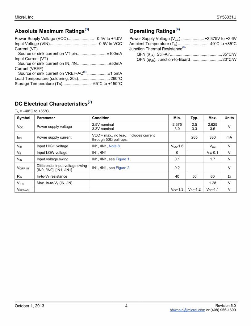
Absolute Maximum Ratings(3) Power Supply Voltage (VCC) ....................... –0.5V to +4.0V Input Voltage (VIN) ......................................... –0.5V to VCC Current (VT) Source or sink current on VT pin.......................... ±100mA Input Current (VT) Source or sink current on IN, /IN ............................ ±50mA Current (VREF) Source or sink current on VREF-AC(5) .................. ±1.5mA Lead Temperature (soldering, 20s) ............................ 260°C Storage Temperature (Ts) ......................... –65°C to +150°C
Operating Ratings(4) Power Supply Voltage (VCC) .................... +2.375V to +3.6V Ambient Temperature (TA) .......................... –40°C to +85°C Junction Thermal Resistance(6) QFN (θJA), Still-Air .............................................. 35°C/W QFN (ψJB), Junction-to-Board ............................ 20°C/W
DC Electrical Characteristics(7) TA = –40°C to +85°C.
Symbol Parameter Condition Min. Typ. Max. Units
VCC Power supply voltage 2.5V nominal 3.3V nominal
2.375 3.0
2.5 3.3
2.625 3.6 V
ICC Power supply current VCC = max., no lead. Includes current through 50Ω pull-ups. 265 330 mA
VIH Input HIGH voltage IN1, /IN1, Note 8 VCC-1.6 VCC V
VIL Input LOW voltage IN1, /IN1 0 VIH-0.1 V
VIN Input voltage swing IN1, /IN1, see Figure 1. 0.1 1.7 V
VDIFF_IN Differential input voltage swing [IN0, /IN0], [IN1, /IN1] IN1, /IN1, see Figure 2. 0.2 V
RIN In-to-VT resistance 40 50 60 Ω
VT IN Max. In-to-VT (IN, /IN) 1.28 V
VREF-AC VCC-1.3 VCC-1.2 VCC-1.1 V

Micrel, Inc. SY58031U
October 1, 2013 5 Revision 5.0 [email protected] or (408) 955-1690
CML DC Electrical Characteristics(7)
VCC = 2.5V ±5% or 3.3V ±10%; RL = 100Ω across Q and /Q; TA = –40°C to +85°C, unless otherwise stated.
Symbol Parameter Condition Min. Typ. Max. Units
VOH Output HIGH voltage VCC-0.02 VCC V
VOUT Output LOW voltage See Figure 1. 325 400 mV
VDIFF_OUT Differential voltage swing See Figure 2. 650 800 mV
ROUT Output source impedance 40 50 60 Ω Notes: 3. Exceeding the absolute maximum ratings may damage the device. 4. The datasheet ratings are not guaranteed if the device is operated beyond the operating ratings. 5. Due to the limited drive capability, use for input of the same package only. 6. Thermal performance assumes exposed pad is soldered (or equivalent) to the device’s most negative potential (GND) on the PCB. ψJB uses 4-layer
θJA in still-air number unless otherwise stated. 7. The device is not guaranteed to function outside its operating ratings. 8. VIH (min.) not lower than 1.2V.
AC Electrical Characteristics(9)
VCC = 2.5V ±5% or 3.3V ±10%; RL = 100Ω across each output pair or equivalent; TA = –40°C to +85°C, unless otherwise stated.
Symbol Parameter Condition Min. Typ. Max. Units
fMAX Maximum operating frequency VOUT ≥200mV clock 6 GHz
tpd Propagation delay (IN-to-Q) 120 230 270 ps
tpd tempco Differential propagation delay temperature coefficient 35 fs/°C
tSKEW Output-to-output (within device) Note 10 7 20 ps
Part-to-part Note 11 100 ps
tJITTER RMS phase jitter Output: 622MHz Integration range 12kHz – 20MHz 75 ps
tr/tf Output rise/fall time 20% to 80% at full output swing. 20 45 60 ps Notes: 9. High frequency AC electricals are guaranteed by design and characterization. All outputs loaded, VIN ≥100mV. 10. Output-to-output skew is measured between outputs under identical transitions. 11. Part-to-part skew is defined for two parts with identical power supply voltages at the same temperature with no skew of the edges at the respective
inputs. Part-to-part skew includes variation in tpd.

Micrel, Inc. SY58031U
October 1, 2013 6 Revision 5.0 [email protected] or (408) 955-1690
Phase Noise Plot
0-10-20-30-40-50-60-70-80-90
-100-110-120-130-140-150-160-170-180-190-200
10 100 1K 10K 100K 1M 10M 100M
OFFSET FREQUENCY (Hz)
NO
ISE
POW
ER (d
Bc/
Hz)
Phase Noise Plot: 622MHz @ 3.3V

Micrel, Inc. SY58031U
October 1, 2013 7 Revision 5.0 [email protected] or (408) 955-1690
Typical Operating Characteristics

Micrel, Inc. SY58031U
October 1, 2013 8 Revision 5.0 [email protected] or (408) 955-1690
Single-Ended and Differential Swings
Figure 1. Single-Ended Voltage Swing Figure 2. Differential Voltage Swing
Timing Diagram

Micrel, Inc. SY58031U
October 1, 2013 9 Revision 5.0 [email protected] or (408) 955-1690
Input Buffer
Figure 3. Simplified Differential Input Buffer
Input Interface Applications
Figure 4. DC-Coupled CML Input Interface
Optional: May connect VT to VCC
Figure 5. AC-Coupled CML Input Interface
Figure 6. LVPECL Input Interface
Figure 7. AC-Coupled LVPECL Input Interface
Figure 8. LVDS Input Interface

Micrel, Inc. SY58031U
October 1, 2013 10 Revision 5.0 [email protected] or (408) 955-1690
CML Output Termination Figure 9 and Figure 10 illustrate how to terminate a CML output using both the AC- and DC-coupled configuration. All outputs of the SY58031U are 50Ω with a 16mA current source.
Figure 9. CML DC-Coupled Termination Figure 10. CML AC-Coupled Termination
Related Micrel Products and Support Documentation Part Number Function Website Link
SY58031U Ultra-Precision 1:8 CML Fanout Buffer with Internal I/O Termination http://www.micrel.com/_PDF/HBW/sy58031u.pdf
SY58032U Ultra-Precision 1:8 LVPECL Fanout Buffer with Internal Termination http://www.micrel.com/_PDF/HBW/sy58032u.pdf
SY58033U Ultra-Precision 1:8 400mV Fanout Buffer with Internal Termination http://www.micrel.com/_PDF/HBW/sy58033u.pdf
HBW Solutions http://www.micrel.com/index.php/en/products/clock-timing.html

Micrel, Inc. SY58031U
October 1, 2013 11 Revision 5.0 [email protected] or (408) 955-1690
Package Information(12, 13)
32-Pin QFN and PCB Thermal Consideration for Package (Always solder, or equivalent, the exposed pad to the PCB)
Note: 12. Package information is correct as of the publication date. For updates and most current information, go to www.micrel.com. 13. Package meets Level 2 qualification. All parts are dry-packaged before shipment. Exposed pads must be soldered to a ground for proper thermal
management.
Micrel, Inc. SY58031U
October 1, 2013 12 Revision 5.0 [email protected] or (408) 955-1690
MICREL, INC. 2180 FORTUNE DRIVE SAN JOSE, CA 95131 USA TEL +1 (408) 944-0800 FAX +1 (408) 474-1000 WEB http://www.micrel.com
Micrel makes no representations or warranties with respect to the accuracy or completeness of the information furnished in this data sheet. This
information is not intended as a warranty and Micrel does not assume responsibility for its use. Micrel reserves the right to change circuitry, specifications and descriptions at any time without notice. No license, whether express, implied, arising by estoppel or otherwise, to any intellectual
property rights is granted by this document. Except as provided in Micrel’s terms and conditions of sale for such products, Micrel assumes no liability whatsoever, and Micrel disclaims any express or implied warranty relating to the sale and/or use of Micrel products including liability or warranties
relating to fitness for a particular purpose, merchantability, or infringement of any patent, copyright or other intellectual property right.
Micrel Products are not designed or authorized for use as components in life support appliances, devices or systems where malfunction of a product can reasonably be expected to result in personal injury. Life support devices or systems are devices or systems that (a) are intended for surgical implant
into the body or (b) support or sustain life, and whose failure to perform can be reasonably expected to result in a significant injury to the user. A Purchaser’s use or sale of Micrel Products for use in life support appliances, devices or systems is a Purchaser’s own risk and Purchaser agrees to fully
indemnify Micrel for any damages resulting from such use or sale.
© 2013 Micrel, Incorporated.