ug0747 user guide polarfire fpga evaluation kit
TRANSCRIPT

UG0747User Guide
PolarFire FPGA Evaluation Kit

50200747. 4.0 2/19
Microsemi HeadquartersOne Enterprise, Aliso Viejo,CA 92656 USAWithin the USA: +1 (800) 713-4113 Outside the USA: +1 (949) 380-6100Sales: +1 (949) 380-6136Fax: +1 (949) 215-4996Email: [email protected]
©2019 Microsemi, a wholly owned
subsidiary of Microchip Technology Inc. All
rights reserved. Microsemi and the
Microsemi logo are registered trademarks of
Microsemi Corporation. All other trademarks
and service marks are the property of their
respective owners.
Microsemi makes no warranty, representation, or guarantee regarding the information contained herein or the suitability of its products and services for any particular purpose, nor does Microsemi assume any liability whatsoever arising out of the application or use of any product or circuit. The products sold hereunder and any other products sold by Microsemi have been subject to limited testing and should not be used in conjunction with mission-critical equipment or applications. Any performance specifications are believed to be reliable but are not verified, and Buyer must conduct and complete all performance and other testing of the products, alone and together with, or installed in, any end-products. Buyer shall not rely on any data and performance specifications or parameters provided by Microsemi. It is the Buyer’s responsibility to independently determine suitability of any products and to test and verify the same. The information provided by Microsemi hereunder is provided “as is, where is” and with all faults, and the entire risk associated with such information is entirely with the Buyer. Microsemi does not grant, explicitly or implicitly, to any party any patent rights, licenses, or any other IP rights, whether with regard to such information itself or anything described by such information. Information provided in this document is proprietary to Microsemi, and Microsemi reserves the right to make any changes to the information in this document or to any products and services at any time without notice.
About Microsemi
Microsemi, a wholly owned subsidiary of Microchip Technology Inc. (Nasdaq: MCHP), offers a comprehensive portfolio of semiconductor and system solutions for aerospace & defense, communications, data center and industrial markets. Products include high-performance and radiation-hardened analog mixed-signal integrated circuits, FPGAs, SoCs and ASICs; power management products; timing and synchronization devices and precise time solutions, setting the world's standard for time; voice processing devices; RF solutions; discrete components; enterprise storage and communication solutions, security technologies and scalable anti-tamper products; Ethernet solutions; Power-over-Ethernet ICs and midspans; as well as custom design capabilities and services. Learn more at www.microsemi.com.

Contents
1 Revision History . . . . . . . . . . . . . . . . . . . . . . . . . . . . . . . . . . . . . . . . . . . . . . . . . . . . . 11.1 Revision 5.0 . . . . . . . . . . . . . . . . . . . . . . . . . . . . . . . . . . . . . . . . . . . . . . . . . . . . . . . . . . . . . . . . . . . . . . . 1
1.2 Revision 4.0 . . . . . . . . . . . . . . . . . . . . . . . . . . . . . . . . . . . . . . . . . . . . . . . . . . . . . . . . . . . . . . . . . . . . . . . 1
1.3 Revision 3.0 . . . . . . . . . . . . . . . . . . . . . . . . . . . . . . . . . . . . . . . . . . . . . . . . . . . . . . . . . . . . . . . . . . . . . . . 1
1.4 Revision 2.0 . . . . . . . . . . . . . . . . . . . . . . . . . . . . . . . . . . . . . . . . . . . . . . . . . . . . . . . . . . . . . . . . . . . . . . . 1
1.5 Revision 1.0 . . . . . . . . . . . . . . . . . . . . . . . . . . . . . . . . . . . . . . . . . . . . . . . . . . . . . . . . . . . . . . . . . . . . . . . 1
2 Getting Started . . . . . . . . . . . . . . . . . . . . . . . . . . . . . . . . . . . . . . . . . . . . . . . . . . . . . 22.1 Kit Contents . . . . . . . . . . . . . . . . . . . . . . . . . . . . . . . . . . . . . . . . . . . . . . . . . . . . . . . . . . . . . . . . . . . . . . . 2
2.2 Block Diagram . . . . . . . . . . . . . . . . . . . . . . . . . . . . . . . . . . . . . . . . . . . . . . . . . . . . . . . . . . . . . . . . . . . . . 3
2.3 Web Resources . . . . . . . . . . . . . . . . . . . . . . . . . . . . . . . . . . . . . . . . . . . . . . . . . . . . . . . . . . . . . . . . . . . . 3
2.4 Board Overview . . . . . . . . . . . . . . . . . . . . . . . . . . . . . . . . . . . . . . . . . . . . . . . . . . . . . . . . . . . . . . . . . . . . 3
2.5 Compatibility With Daughter Boards . . . . . . . . . . . . . . . . . . . . . . . . . . . . . . . . . . . . . . . . . . . . . . . . . . . . 6
2.6 Handling the Board . . . . . . . . . . . . . . . . . . . . . . . . . . . . . . . . . . . . . . . . . . . . . . . . . . . . . . . . . . . . . . . . . 6
2.7 Powering Up the Board . . . . . . . . . . . . . . . . . . . . . . . . . . . . . . . . . . . . . . . . . . . . . . . . . . . . . . . . . . . . . . 7
3 Installation and Settings . . . . . . . . . . . . . . . . . . . . . . . . . . . . . . . . . . . . . . . . . . . . . . 83.1 Software Settings . . . . . . . . . . . . . . . . . . . . . . . . . . . . . . . . . . . . . . . . . . . . . . . . . . . . . . . . . . . . . . . . . . . 8
3.2 Hardware Settings . . . . . . . . . . . . . . . . . . . . . . . . . . . . . . . . . . . . . . . . . . . . . . . . . . . . . . . . . . . . . . . . . . 83.2.1 Jumper Settings . . . . . . . . . . . . . . . . . . . . . . . . . . . . . . . . . . . . . . . . . . . . . . . . . . . . . . . . . . . . . 83.2.2 LEDs . . . . . . . . . . . . . . . . . . . . . . . . . . . . . . . . . . . . . . . . . . . . . . . . . . . . . . . . . . . . . . . . . . . . . 93.2.3 Test Points . . . . . . . . . . . . . . . . . . . . . . . . . . . . . . . . . . . . . . . . . . . . . . . . . . . . . . . . . . . . . . . . 10
3.3 Power Sources . . . . . . . . . . . . . . . . . . . . . . . . . . . . . . . . . . . . . . . . . . . . . . . . . . . . . . . . . . . . . . . . . . . . 10
4 Board Components and Operations . . . . . . . . . . . . . . . . . . . . . . . . . . . . . . . . . . . . 134.1 Memory Interface . . . . . . . . . . . . . . . . . . . . . . . . . . . . . . . . . . . . . . . . . . . . . . . . . . . . . . . . . . . . . . . . . . 13
4.1.1 DDR3 . . . . . . . . . . . . . . . . . . . . . . . . . . . . . . . . . . . . . . . . . . . . . . . . . . . . . . . . . . . . . . . . . . . . 134.1.2 DDR4 . . . . . . . . . . . . . . . . . . . . . . . . . . . . . . . . . . . . . . . . . . . . . . . . . . . . . . . . . . . . . . . . . . . . 13
4.2 SPI Serial Flash . . . . . . . . . . . . . . . . . . . . . . . . . . . . . . . . . . . . . . . . . . . . . . . . . . . . . . . . . . . . . . . . . . . 14
4.3 Transceivers . . . . . . . . . . . . . . . . . . . . . . . . . . . . . . . . . . . . . . . . . . . . . . . . . . . . . . . . . . . . . . . . . . . . . 144.3.1 XCVR0 Interface . . . . . . . . . . . . . . . . . . . . . . . . . . . . . . . . . . . . . . . . . . . . . . . . . . . . . . . . . . . 144.3.2 XCVR1 and XCVR3 Interface . . . . . . . . . . . . . . . . . . . . . . . . . . . . . . . . . . . . . . . . . . . . . . . . . 154.3.3 XCVR2 Interface . . . . . . . . . . . . . . . . . . . . . . . . . . . . . . . . . . . . . . . . . . . . . . . . . . . . . . . . . . . 164.3.4 XCVR Reference Clocks . . . . . . . . . . . . . . . . . . . . . . . . . . . . . . . . . . . . . . . . . . . . . . . . . . . . . 17
4.4 Microsemi PHY (VSC8575) . . . . . . . . . . . . . . . . . . . . . . . . . . . . . . . . . . . . . . . . . . . . . . . . . . . . . . . . . . 184.4.1 Microsemi 1588v2 (ZL30364GDG2) . . . . . . . . . . . . . . . . . . . . . . . . . . . . . . . . . . . . . . . . . . . . 18
4.5 Power Monitoring . . . . . . . . . . . . . . . . . . . . . . . . . . . . . . . . . . . . . . . . . . . . . . . . . . . . . . . . . . . . . . . . . . 19
4.6 Programming . . . . . . . . . . . . . . . . . . . . . . . . . . . . . . . . . . . . . . . . . . . . . . . . . . . . . . . . . . . . . . . . . . . . . 204.6.1 FTDI . . . . . . . . . . . . . . . . . . . . . . . . . . . . . . . . . . . . . . . . . . . . . . . . . . . . . . . . . . . . . . . . . . . . . 20
4.7 System Reset . . . . . . . . . . . . . . . . . . . . . . . . . . . . . . . . . . . . . . . . . . . . . . . . . . . . . . . . . . . . . . . . . . . . . 21
4.8 50 MHz Oscillator . . . . . . . . . . . . . . . . . . . . . . . . . . . . . . . . . . . . . . . . . . . . . . . . . . . . . . . . . . . . . . . . . . 21
4.9 User Interface . . . . . . . . . . . . . . . . . . . . . . . . . . . . . . . . . . . . . . . . . . . . . . . . . . . . . . . . . . . . . . . . . . . . 214.9.1 User LEDs . . . . . . . . . . . . . . . . . . . . . . . . . . . . . . . . . . . . . . . . . . . . . . . . . . . . . . . . . . . . . . . . 224.9.2 Push-Button Switches . . . . . . . . . . . . . . . . . . . . . . . . . . . . . . . . . . . . . . . . . . . . . . . . . . . . . . . 224.9.3 Slide Switches (DPDT) . . . . . . . . . . . . . . . . . . . . . . . . . . . . . . . . . . . . . . . . . . . . . . . . . . . . . . 234.9.4 DIP Switches (SPST) . . . . . . . . . . . . . . . . . . . . . . . . . . . . . . . . . . . . . . . . . . . . . . . . . . . . . . . 234.9.5 FMC HPC Connector . . . . . . . . . . . . . . . . . . . . . . . . . . . . . . . . . . . . . . . . . . . . . . . . . . . . . . . . 244.9.6 FMC Connector - HPC (J34) . . . . . . . . . . . . . . . . . . . . . . . . . . . . . . . . . . . . . . . . . . . . . . . . . . 24
Microsemi Proprietary and Confidential UG0747 User Guide Revision 4.0 iii

5 Pin List . . . . . . . . . . . . . . . . . . . . . . . . . . . . . . . . . . . . . . . . . . . . . . . . . . . . . . . . . . . 31
6 Board Component Placement . . . . . . . . . . . . . . . . . . . . . . . . . . . . . . . . . . . . . . . . . 32
7 Appendix: Running the Demo Design . . . . . . . . . . . . . . . . . . . . . . . . . . . . . . . . . . . 33
8 Appendix: Programming PolarFire FPGA Using the On-Board FlashPro5 . . . . . . . 34
9 Appendix: Power Monitoring . . . . . . . . . . . . . . . . . . . . . . . . . . . . . . . . . . . . . . . . . . 359.1 Prerequisites . . . . . . . . . . . . . . . . . . . . . . . . . . . . . . . . . . . . . . . . . . . . . . . . . . . . . . . . . . . . . . . . . . . . . 35
9.2 Installing PowerMonitor . . . . . . . . . . . . . . . . . . . . . . . . . . . . . . . . . . . . . . . . . . . . . . . . . . . . . . . . . . . . . 36
9.3 About Microsemi PowerMonitor . . . . . . . . . . . . . . . . . . . . . . . . . . . . . . . . . . . . . . . . . . . . . . . . . . . . . . . 36
10 Appendix: Performance Data . . . . . . . . . . . . . . . . . . . . . . . . . . . . . . . . . . . . . . . . . 3810.1 Setup Details . . . . . . . . . . . . . . . . . . . . . . . . . . . . . . . . . . . . . . . . . . . . . . . . . . . . . . . . . . . . . . . . . . . . . 38
10.2 JESD204B Results . . . . . . . . . . . . . . . . . . . . . . . . . . . . . . . . . . . . . . . . . . . . . . . . . . . . . . . . . . . . . . . . 39
10.3 10BASE-G KR . . . . . . . . . . . . . . . . . . . . . . . . . . . . . . . . . . . . . . . . . . . . . . . . . . . . . . . . . . . . . . . . . . . . 40
10.4 Interlaken . . . . . . . . . . . . . . . . . . . . . . . . . . . . . . . . . . . . . . . . . . . . . . . . . . . . . . . . . . . . . . . . . . . . . . . . 41
10.5 CPRI . . . . . . . . . . . . . . . . . . . . . . . . . . . . . . . . . . . . . . . . . . . . . . . . . . . . . . . . . . . . . . . . . . . . . . . . . . . 42
11 Appendix: Errata . . . . . . . . . . . . . . . . . . . . . . . . . . . . . . . . . . . . . . . . . . . . . . . . . . . 4311.1 Errata Descriptions . . . . . . . . . . . . . . . . . . . . . . . . . . . . . . . . . . . . . . . . . . . . . . . . . . . . . . . . . . . . . . . . 43
11.1.1 Hot swapping is not supported on Programming headers J32, J29, PCIe CONN (CON3), SFP+ cage (J36), GPIO headers (J7, J8) 43
11.1.2 The VDDI3 (Bank 3) supply voltage is higher than the Datasheet specification . . . . . . . . . . . 43
Microsemi Proprietary and Confidential UG0747 User Guide Revision 4.0 iv

Microsemi Proprietary and Confidential UG0747 User Guide Revision 4.0 v
Figures
Figure 1 PolarFire Evaluation Kit Block Diagram . . . . . . . . . . . . . . . . . . . . . . . . . . . . . . . . . . . . . . . . . . . . . . 3Figure 2 PolarFire Evaluation Board . . . . . . . . . . . . . . . . . . . . . . . . . . . . . . . . . . . . . . . . . . . . . . . . . . . . . . . . 4Figure 3 Voltage Rails in PolarFire Evaluation Board . . . . . . . . . . . . . . . . . . . . . . . . . . . . . . . . . . . . . . . . . . 11Figure 4 DDR3 Memory Interface . . . . . . . . . . . . . . . . . . . . . . . . . . . . . . . . . . . . . . . . . . . . . . . . . . . . . . . . . 13Figure 5 DDR4 Memory Interface . . . . . . . . . . . . . . . . . . . . . . . . . . . . . . . . . . . . . . . . . . . . . . . . . . . . . . . . . 14Figure 6 SPI Flash Interface . . . . . . . . . . . . . . . . . . . . . . . . . . . . . . . . . . . . . . . . . . . . . . . . . . . . . . . . . . . . . 14Figure 7 XCVR0 Interface . . . . . . . . . . . . . . . . . . . . . . . . . . . . . . . . . . . . . . . . . . . . . . . . . . . . . . . . . . . . . . . 15Figure 8 XCVR1 and XCVR3 Interface . . . . . . . . . . . . . . . . . . . . . . . . . . . . . . . . . . . . . . . . . . . . . . . . . . . . . 16Figure 9 XCVR2 Interface . . . . . . . . . . . . . . . . . . . . . . . . . . . . . . . . . . . . . . . . . . . . . . . . . . . . . . . . . . . . . . . 17Figure 10 XCVR Reference Clocks . . . . . . . . . . . . . . . . . . . . . . . . . . . . . . . . . . . . . . . . . . . . . . . . . . . . . . . . 18Figure 11 PHY Interface . . . . . . . . . . . . . . . . . . . . . . . . . . . . . . . . . . . . . . . . . . . . . . . . . . . . . . . . . . . . . . . . . 19Figure 12 Power Management . . . . . . . . . . . . . . . . . . . . . . . . . . . . . . . . . . . . . . . . . . . . . . . . . . . . . . . . . . . . 20Figure 13 FTDI Interface . . . . . . . . . . . . . . . . . . . . . . . . . . . . . . . . . . . . . . . . . . . . . . . . . . . . . . . . . . . . . . . . . 21Figure 14 50 MHz Clock Oscillator . . . . . . . . . . . . . . . . . . . . . . . . . . . . . . . . . . . . . . . . . . . . . . . . . . . . . . . . . 21Figure 15 LED Interface . . . . . . . . . . . . . . . . . . . . . . . . . . . . . . . . . . . . . . . . . . . . . . . . . . . . . . . . . . . . . . . . . 22Figure 16 Switches Interface . . . . . . . . . . . . . . . . . . . . . . . . . . . . . . . . . . . . . . . . . . . . . . . . . . . . . . . . . . . . . 23Figure 17 SPST Interface . . . . . . . . . . . . . . . . . . . . . . . . . . . . . . . . . . . . . . . . . . . . . . . . . . . . . . . . . . . . . . . . 24Figure 18 Silkscreen Top View . . . . . . . . . . . . . . . . . . . . . . . . . . . . . . . . . . . . . . . . . . . . . . . . . . . . . . . . . . . . 32Figure 19 Silkscreen Bottom View . . . . . . . . . . . . . . . . . . . . . . . . . . . . . . . . . . . . . . . . . . . . . . . . . . . . . . . . . 32Figure 20 Selecting the On-Board FlashPro5 . . . . . . . . . . . . . . . . . . . . . . . . . . . . . . . . . . . . . . . . . . . . . . . . . 34Figure 21 Power Monitoring Block Diagram . . . . . . . . . . . . . . . . . . . . . . . . . . . . . . . . . . . . . . . . . . . . . . . . . . 35Figure 22 PowerMonitor GUI . . . . . . . . . . . . . . . . . . . . . . . . . . . . . . . . . . . . . . . . . . . . . . . . . . . . . . . . . . . . . 36Figure 23 Hardware Setup for Measurement . . . . . . . . . . . . . . . . . . . . . . . . . . . . . . . . . . . . . . . . . . . . . . . . . 38Figure 24 JESD204B Eye Diagram With De-embedding . . . . . . . . . . . . . . . . . . . . . . . . . . . . . . . . . . . . . . . . 39Figure 25 10BASE-G KR Data Eye Diagram . . . . . . . . . . . . . . . . . . . . . . . . . . . . . . . . . . . . . . . . . . . . . . . . . 40Figure 26 Interlaken Data Eye Diagram . . . . . . . . . . . . . . . . . . . . . . . . . . . . . . . . . . . . . . . . . . . . . . . . . . . . . 41Figure 27 CPRI Data Eye Diagram . . . . . . . . . . . . . . . . . . . . . . . . . . . . . . . . . . . . . . . . . . . . . . . . . . . . . . . . . 42

Microsemi Proprietary and Confidential UG0747 User Guide Revision 4.0 vi
Tables
Table 1 Kit Contents . . . . . . . . . . . . . . . . . . . . . . . . . . . . . . . . . . . . . . . . . . . . . . . . . . . . . . . . . . . . . . . . . . . 2Table 2 PolarFire Evaluation Board Components . . . . . . . . . . . . . . . . . . . . . . . . . . . . . . . . . . . . . . . . . . . . . 4Table 3 Jumper Settings . . . . . . . . . . . . . . . . . . . . . . . . . . . . . . . . . . . . . . . . . . . . . . . . . . . . . . . . . . . . . . . . 8Table 4 LEDs . . . . . . . . . . . . . . . . . . . . . . . . . . . . . . . . . . . . . . . . . . . . . . . . . . . . . . . . . . . . . . . . . . . . . . . . . 9Table 5 Test Points . . . . . . . . . . . . . . . . . . . . . . . . . . . . . . . . . . . . . . . . . . . . . . . . . . . . . . . . . . . . . . . . . . . 10Table 6 I/O Voltage Rails . . . . . . . . . . . . . . . . . . . . . . . . . . . . . . . . . . . . . . . . . . . . . . . . . . . . . . . . . . . . . . . 10Table 7 Power Regulators . . . . . . . . . . . . . . . . . . . . . . . . . . . . . . . . . . . . . . . . . . . . . . . . . . . . . . . . . . . . . . 11Table 8 User LEDs . . . . . . . . . . . . . . . . . . . . . . . . . . . . . . . . . . . . . . . . . . . . . . . . . . . . . . . . . . . . . . . . . . . 22Table 9 Push-Button Switches . . . . . . . . . . . . . . . . . . . . . . . . . . . . . . . . . . . . . . . . . . . . . . . . . . . . . . . . . . . 22Table 10 DIP Switches . . . . . . . . . . . . . . . . . . . . . . . . . . . . . . . . . . . . . . . . . . . . . . . . . . . . . . . . . . . . . . . . . 23Table 11 J34 FMC Connector Pinout . . . . . . . . . . . . . . . . . . . . . . . . . . . . . . . . . . . . . . . . . . . . . . . . . . . . . . 24Table 12 JESD204B Jitter Measurements . . . . . . . . . . . . . . . . . . . . . . . . . . . . . . . . . . . . . . . . . . . . . . . . . . . 39Table 13 10BASE-G KR Jitter Measurements . . . . . . . . . . . . . . . . . . . . . . . . . . . . . . . . . . . . . . . . . . . . . . . . 40Table 14 Interlaken Jitter Measurements . . . . . . . . . . . . . . . . . . . . . . . . . . . . . . . . . . . . . . . . . . . . . . . . . . . 41Table 15 CPRI Jitter Measurements . . . . . . . . . . . . . . . . . . . . . . . . . . . . . . . . . . . . . . . . . . . . . . . . . . . . . . . 42

Revision History
Microsemi Proprietary and Confidential UG0747 User Guide Revision 4.0 1
1 Revision History
The revision history describes the changes that were implemented in the document. The changes are listed by revision, starting with the most current publication.
1.1 Revision 5.0Added Table 7, page 11 that lists the suggested power regulators.
1.2 Revision 4.0Added performance measurement data for different protocols, see Appendix: Performance Data, page 38.
1.3 Revision 3.0Updated Figure 18, page 32 and Figure 19, page 32.
1.4 Revision 2.0Updated Appendix: Power Monitoring, page 35.
1.5 Revision 1.0The first publication of this document.

Getting Started
2 Getting Started
The Microsemi PolarFire™ FPGA Evaluation Kit (MPF300-EVAL-KIT), which is RoHS-compliant, enables you to evaluate the PolarFire family of FPGAs with support for the following interfaces:
• PCI Express Gen1 and Gen2• 1 GbE• DDR3 and DDR4 memory• FMC HPC with 8 Transceiver lanes• 1 Full-Duplex Transceiver SMAs• SFP+ Cage• UART Interface to FTDI device• SPI Interface to SPI Flash device
2.1 Kit ContentsThe following table lists the contents of the PolarFire FPGA Evaluation Kit.
Note: The PolarFire device is programmed using the on-board FlashPro5 programmer. The on-board FlashPro5 programmer is used to develop and debug embedded applications using SoftConsole, Identify, or SmartDebug.
For more information, see UG0726: PolarFire FPGA Board Design User Guide.
Table 1 • Kit Contents
Item Quantity
PolarFire Evaluation Board (printed circuit board) featuring MPF300TS-1FCG1152I device with 300K logic elements
1
12 V/5 A wall-mounted power adapter 1
USB 2.0 A male to mini-USB B cable for UART/power interface (up to 1 A) to PC
1
Quickstart card 1
Free one-year Libero Gold software license 1
Microsemi Proprietary and Confidential UG0747 User Guide Revision 4.0 2

Getting Started
2.2 Block DiagramThe following block diagram shows all of the components of the PolarFire Evaluation Board.
Figure 1 • PolarFire Evaluation Kit Block Diagram
2.3 Web ResourcesFor more information about the PolarFire Evaluation Board, see https://www.microsemi.com/products/fpga-soc/design-resources/dev-kits/polarfire/polarfire-eval-kit.
2.4 Board OverviewThe PolarFire Evaluation Board features the PolarFire MPF300TS-1FCG1152I FPGA. The device has the following capabilities:
• 20 Kb dual-port or two-port large static random access memory (LSRAM) block with a built-in single error correct double error detect (SECDED)
• 64 × 12 two-port µSRAM block implemented as an array of latches• 18 × 18 Multiply Accumulate (MACC) block with a pre-adder, a 48-bit accumulator, and an optional
16 deep × 18 coefficient RO• Built-in µPROM, modifiable at program time, readable at run time for user data storage• Digest integrity check for FPGA, µPROM, and sNVM• Low-power features:
• Low device static power• Low inrush current
PolarFire FPGA – MPF300TS-1FCG1152I
VSC8575PHY
FT4232 USB mini B connector
SGMII X2
DDR3 MT41K1G8SN-12516 Gb (128*8*16)
HSIOBank1
JTAGBank3
GPIOBank 4
DDR4 MT40A1G8WE-
083E:B32 Gb (1G*32)
HSIOBank0, 7
Lane 2, 3
REFCLK1
Debug LEDs-8HSIOBank6
Mux
XCVR 2
XCVR 2 SFP ConnectorLane 1
J36
On Board Oscillator-
122.88 MHz
1588 REFCLK 125MHz
1588 REFCLK
125 MHz CLK
GPIOBank 4
A2F200M3F-1FGG256I
JumperJ18,19,20,21,22
Port A
JTAG
DEMUX
0
1
MUX
U72
MUX
U39
U38
JTAGHeader
0
1
J72
J29
1
0
MUX
U71 SPIExternal
Flash (1 Gb)
U44
1
0
SC-SPIBank3
S
SS
SPI SIGNALS
JTAG SIGNALS
UART
Debug Switchs-8 HSIOBank6
J5
HSIOBank6 HSIO
Bank6
UART SIGNALS
XCVR 2 REFCLK
S
On Board Oscillator-50 MHz
On Board Oscillator-125 MHz
RJ4510/100/1000
Mbps
RJ4510/100/1000
Mbps
ZL30364GDG2On Board Oscillator-
24.576 MHz
SPIHeader
Port C
Port D
FMC HPC Connector PCIe edge connector
HSIOBank6
GPIOBank4
SPI flash(1Gb)MT25QU01GBBB
8ESF-0SIT
GPIOBank 5
XCVR1,3
U45 J34
8 Lanes HPC[HB0:21] HPC[HA0:23] LPC[0:33]
GPIOBank2
XCVR 0
Lane 4 REFCLK0
CON3On Board Oscillator-
156.25 MHz
XCVR_0A_REFCLK
XCVR_2C_REFCLK
XCVR 2Lane 0 SMA
Connectors
XCVR_2B_REFCLKSMA
ConnectorsClock
System_Controller
The JTAG programming data goes to the System_Controller and then from SC_SPI bank3 it goes to the external
SPI flash device.
J28 JumperGND
GNDJ28 Jumper
GNDJ26 Jumper
J27 JumperGND
Microsemi Proprietary and Confidential UG0747 User Guide Revision 4.0 3
Getting Started
• Low power transceivers• Unique Flash*Freeze (F*F) mode• High-performance communication interfaces
The PolarFire Evaluation Board has several standard interfaces, including:
• VSC8575 with two RJ45 connector for 10\100\1000 Mbps Ethernet• 8 Full-Duplex Transceiver lanes connected through FMC connector• FMC HPC connector• DDR3 memory• DDR4 memory• Power Sequence and monitor chip• x4 Lane PCIe Edge connector• SFP+ connector• Two SPI Flash devices
The PolarFire Evaluation Board has 14 layers and it is manufactured using NElco-SI material for top and bottom layers, and FR4 dielectric material for inner layers.
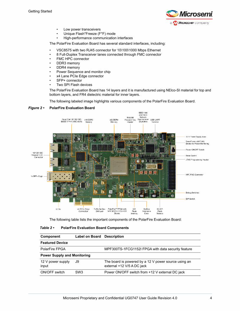
The following labeled image highlights various components of the PolarFire Evaluation Board.
Figure 2 • PolarFire Evaluation Board
The following table lists the important components of the PolarFire Evaluation Board:
Table 2 • PolarFire Evaluation Board Components
Component Label on Board Description
Featured Device
PolarFire FPGA MPF300TS-1FCG1152I FPGA with data security feature
Power Supply and Monitoring
12 V power supply input
J9 The board is powered by a 12 V power source using an external +12 V/5 A DC jack
ON/OFF switch SW3 Power ON/OFF switch from +12 V external DC jack
Microsemi Proprietary and Confidential UG0747 User Guide Revision 4.0 4

Getting Started
Power Monitoring FPGA
U27 Microsemi SmartFusion FPGA (A2F200M3F-1FGG256I) used for power sequence and monitoring the voltage rails on the PolarFire Evaluation Board
Clocks
On-board 50 MHz clock oscillator
Y9 50 MHz clock oscillator with single-ended output
XCVR reference clock connectors
J40 and J44 SMA connectors (used by external clock source)
OSC Y6 122.88 MHz oscillator (differential LVDS output) is the input to the DS08MB200TSQ clock MUX buffer
OSC Y4 125 MHz oscillator (differential LVDS output) is the input to the DS08MB200TSQ clock MUX buffer
OSC Y5 156.25 MHz oscillator (differential LVDS output) provides the REFCLK to XCVRs connected to the PolarFire device pins AC27 and AC28
Clock Network synchronous chip
U16 ZL30364GDG2 IEEE 1588 & Synchronous Ethernet Packet Clock Network Synchronizer that provides the clock to VSC8575 and the PolarFire device
Clock MUX\Buffer U58 DS08MB200TSQ_NOPB (differential LVDS output) provides the REFCLK to XCVRs connected to PolarFire device pins AE27 and AE28
FPGA Programming and Debugging
USB - UART terminal J5 FTDI programmer interface to program the external SPI flash and the PolarFire deviceThe J5 cable powers up the SmartFusion and the FTDI device that are required for power monitoring. The J5 and J9 cables must be connected to power up the board.
SPI flash U44 and U45 Two 1 Gb SPI flash Micron MT25QL01GBBB8ESF-0SIT connected to SPI pins on bank 3 and bank 6 of the PolarFire device
FT4232H U29 USB-to-quad serial ports in various configurations
JTAG programming header
J32 This header is used to program and debug the PolarFire device using FlashPro4 or FlashPro5. In the FlashPro software, the appropriate programmer (FlashPro4 or FlashPro5) must be selected.
Communication Interfaces
x4 PCIe edge connector
PCIe edge connector with four lanes
Tx/Rx XCVR2 SMA pairs
J41J42J37J38
XCVR0 TXD0PXCVR0 TXD0NXCVR0 RXD0PXCVR0 RXD0N
Two 10/100/1000 Ethernet RJ45 connectors
J15 and J30 Ethernet (RJ45) jacks with external magnetics interfacing with Microsemi quad 10/100/1000 BASE-T PHY chip and 1588 timing feature in SGMII mode. VSC8575 interfaces with the Ethernet ports of the PolarFire device
Table 2 • PolarFire Evaluation Board Components (continued)
Component Label on Board Description
Microsemi Proprietary and Confidential UG0747 User Guide Revision 4.0 5

Getting Started
2.5 Compatibility With Daughter BoardsDaughter boards with FMC connectors can be plugged into the PolarFire Evaluation board.
2.6 Handling the BoardPay attention to the following points while handling or operating the board to avoid possible damage or malfunction:
• Handle the board with electrostatic discharge (ESD) precautions to avoid damage. For information about using the board with ESD precautions, see https://www.microsemi.com/document-portal/doc_view/126483-esd-appnote.
• Power down the board to switch between Programming headers J32, J29, PCIe CONN (CON3), SFP+ cage (J36), and GPIO headers (J7, J8).
FMC HPC connector J34 FMC connector with eight XCVR lanes and 80 Differential pairs (HPC[HB0:21], HPC[HA0:23] and LPC[0:33])
SFP+ connector J36 SFP connector of one XCVR lane to support the optical interface with an external interface
Memory Chips
DDR3 Memory U18 and U19 Two 8 Gb (MT41K1G8SN-125:A- 128 Meg × 8 × 8) chips are connected in Fly-by topology with a 16-bit data bus for storing data bitsFor more information, download the datasheet from https://www.micron.com/parts/dram/ddr3-sdram/mt41k1g8sn-125?pc=00EED26F-83AE-4CE6-9A28-EB8B033361E8
DDR4 Memory U36, U42, U47, and U48
Four 8 Gb (MT41K1G8SN-125:A- 1G Meg × 8) chips are connected in Fly-by topology with a 32-bit data bus for storing data bitsFor more information, download the datasheet from https://www.micron.com/parts/dram/ddr4-sdram/mt40a1g8we-083e?pc=0759757A-85DB-4AD3-9B4D-B7E7DDE8A22D
General Purpose I/O
Switches SW7, SW8, SW9, and SW10
Push-button switches for user-interface debugging applications
DIP Switches SW11 Eight DIP switches for testing
Light-emitting diodes (LEDs)
Eight active-high LEDs connected to some of the user I/Os for debugging, and twelve active high LEDs used for indicating power supply
Reset switch SW6 Push-button system reset for the PolarFire deviceUsers must program this GPIO for PolarFire device reset function
Table 2 • PolarFire Evaluation Board Components (continued)
Component Label on Board Description
Microsemi Proprietary and Confidential UG0747 User Guide Revision 4.0 6

Getting Started
2.7 Powering Up the BoardThe PolarFire Evaluation Board is powered up using either the 12 V DC jack or the PCIe connector.
To power up the board, connect the 12 V DC jack to the board, and connect the J5 USB port to the host PC.
Note: If the J5 USB port is not connected to the Host, the board will not power up even if the 12 V supply is on.
The PolarFire Evaluation Board ships with a pre-programmed bring-up design (LED toggling). Install the software required for developing designs and set the jumpers for the pre-programmed design. For more information, see Installation and Settings, page 8.
Microsemi Proprietary and Confidential UG0747 User Guide Revision 4.0 7

Installation and Settings
3 Installation and Settings
This section provides information about the software and hardware settings required to run the pre-programmed demo design on the PolarFire Evaluation Board.
3.1 Software SettingsDownload and install the latest release of Microsemi Libero® SoC PolarFire from the Microsemi website, and register for a free one-year Libero Gold software license. The Libero SoC PolarFire installer includes FlashPro5 drivers. For instructions about installing Libero SoC PolarFire and SoftConsole, see the Libero Software Installation and Licensing Guide. For instructions about how to download and install Microsemi DirectCores and driver firmware cores on the PC where Libero SoC is installed, see the Installing IP Cores and Drivers User’s Guide.
3.2 Hardware SettingsThis section provides information about jumper settings, switches, LEDs, and DIP switches on the PolarFire Evaluation Board.
3.2.1 Jumper SettingsConnect the jumpers according to the settings specified in the following table.
Table 3 • Jumper Settings
Jumper Description Pin Default Setting
J18, J19, J20, J21, J22
Jumpers to select the PolarFire JTAG or A2F JTAG
Close pin 1 and 2 for programming the power sequence and monitoring chip through the FTDI
Close pin 2 and 3 for programming the PolarFire FPGA through FTDIUser must always retain the default jumper setting
Open
Closed
J46 Jumper to select switch-side MUX inputs of A or B to the line side
Close pin 1 and 2 (Input A to the line side) for routing the on-board 122.88 MHz differential clock oscillator output to the line side
Close pin 1 and 2 (Input B to the line side) for routing the on-board 125 MHz differential clock oscillator output to the line side
Open
Closed
J28 Jumper to select the external JTAG or the on-board FlashPro5 for programming the PolarFire device
Close pin 1and 2 for programming through the on-board FlashPro5
Open
J26 Jumper to select the FTDI SPI or SC_SPI header
Close pin 1 and 2 for programming through the SC_SPI Header
Open
Microsemi Proprietary and Confidential UG0747 User Guide Revision 4.0 8

Installation and Settings
For locations of various jumpers and test points on the PolarFire Evaluation Board, see Figure 18, page 32.
3.2.2 LEDsThe following table lists the power supply and Ethernet LEDs.
J27 Jumper to select between FTDI SPI or External SPI Flash to program the device
Close pin 1 and 2 for programming through the External SPI flash
Open
J23 Jumper to define the SPI interface mode
Close pin 1 and 2 to define the SPI Slave mode Open
J4 Jumper to select the SW3 input or the ENABLE_FT4232 signal from the FT4232H chip
Close pin 1 and 2 for manual power switching using SW3
Close pin 2 and 3 for remote power switching using the GPIO capability of the FT4232 chip
Closed
Open
J12 Jumper to select the PolarFire VCCIO voltage (VCCIO_HPC_VADJ) to 1.2V, 1.5V, 1.8V, 2.5V, or 3.3V
Close pin 1 and 2 for 3.3 VClose pin 3 and 4 for 2.5 VClose pin 5 and 6 for 1.8 VClose pin 7 and 8 for 1.5 VClose pin 9 and 10 for 1.2 V
OpenClosedOpenOpenOpen
J43 Jumper to select the VDD voltage
close Pin 1 and 2 for 1.05V Open
Table 4 • LEDs
LED Description
DS3 - Green 1 V Voltage rail
DS4 - Green 1.5 V Voltage rail
DS5 - Green 0.75 V Voltage rail
DS6 - Green 1.2 V Voltage rail
DS7 - Green 0.6 V Voltage rail
DS8 - Green 1.8 V Voltage rail
DS9 - Green 1.0 V Voltage rail for VSC8575
DS10 - Green 1.0 V Voltage rail for VDDA
DS11 - Green VDDAUX_GPIO Voltage rail
DS12 - Green 2.5 V Voltage rail
Table 3 • Jumper Settings
Jumper Description Pin Default Setting
Microsemi Proprietary and Confidential UG0747 User Guide Revision 4.0 9

Installation and Settings
3.2.3 Test PointsThe following table lists USB, ground, and other test points.
3.3 Power SourcesThe PolarFire Evaluation Board uses Microsemi power supply devices. For more information about power supply devices, see www.microsemi.com/product-directory/ics/853- power-management.
The following table lists the key power supplies required for normal operation of the PolarFire Evaluation Board.
DS13- Green VCCIO_HPC_VADJ voltage
DS14 - Green VDDAUX Voltage rail
DS18 - Green 12 V voltage rail
DS16 - Green 5 V voltage rail
DS17 - Green 3.3 V voltage rail
Table 5 • Test Points
Test Point Description
TP12 Test point to probe the voltage of 1P8V_ZL
TP18 Test point to probe 5V voltage
TP12 Test point to probe 3.3V voltage
TP126 Test point to probe 1V voltage
TP22 Test point to probe 1.5 V voltage for DDR3
TP8 Test point to probe 0.75 V
TP12 1.5V current-sensing test point
TP115 Test point to probe 1.2 V voltage for DDR4
TP109 Test point to probe 0.6V voltage
TP124 Test point to probe 1.8 V voltage
TP23 Test point to probe 1 V voltage of VSC8575 PHY
TP123 Test point to probe 1.0 V (VDDA)
TP30 Test point to probe VDDAUX voltage
TP16 Test point to probe IO voltage
TP33 Test point to probe AUX voltage
TP118, 130,15,119,129,29,121,128,19,3
Ground
Table 6 • I/O Voltage Rails
PolarFire Bank I/O Rail Voltage
Bank 0 1P5V_REG 1.5 V
Bank 1 1P2V_REG 1.2 V
Table 4 • LEDs (continued)
LED Description
Microsemi Proprietary and Confidential UG0747 User Guide Revision 4.0 10

Installation and Settings
Note: The Bank 3 voltage is set to 3.3 V for Rev B board, this voltage has been updated in Rev C boards to 2.5 V as per the datasheet. Designers should use 2.5 V for building their own boards.
The following figure shows voltage rails (12 V, 5 V, 3.3 V, 2.5 V, 1.8 V, 1.5 V, and 1.0 V) available on the PolarFire Evaluation Board.
Figure 3 • Voltage Rails in PolarFire Evaluation Board
The following table lists the suggested Microchip power regulators for PolarFire FPGA voltage rails.
Bank 2 VCCIO_HPC_VADJ 3.3 V, 2.5 V, 1.8 V, 1.5 V, or 1.2 V
Bank 3 3P3V 3.3 V
Bank 4 VCCIO_HPC_VADJ 3.3 V, 2.5 V, 1.8 V, 1.5 V, or 1.2 V
Bank 5 VCCIO_HPC_VADJ 3.3 V, 2.5 V, 1.8 V, 1.5 V, or 1.2 V
Bank 6 1P8V 1.8V
Bank 7 1P2V_REG 1.2VVDD_XCVR_CLK VDD25_DUT 2P5V
Table 7 • Power Regulators1
Voltage rail Part Number Description Current
5V MIC24055YJL-TR IC REG BUCK ADJ 12A SYNC 28QFN 12A
Table 6 • I/O Voltage Rails (continued)
PolarFire Bank I/O Rail Voltage
12V
Gate
12V DC - JACK
12VO_IN
IRF_12V U7Switching Regulator
U56Switching Regulator
U57Switching Regulator
VDD1.0 V
3.3 V
U20Switching Regulator
U5switching Regulator
U21Switching Regulator
U54Switching Regulator
5 V
VDDAUX[2, 4]
VDD25/VDDA25/VDD_XCVR_CLK
2.5 V
Bank Supply
VDDAUX5
1.8 VVDD18/Bank Supply
2.5 V/3.3 V
2.5 V/3.3 V
U10Switching Regulator
U49Switching Regulator
1.5 V
1.2 VBank Supply
Bank Supply
U6Linear
Regulator
U46Linear
Regulator
DDR4-VTT0.6 V
DDR3-VTT0.75 V
PMOS SwitchGate
PMOS SwitchGate
Main ON/OFF Switch A2F200M3F
U55Linear Regulator
VDDA1.0V
U52Linear Regulator
1.2/2.5/1.8/1.5/1.2 V
Microsemi Proprietary and Confidential UG0747 User Guide Revision 4.0 11

Installation and Settings
VDD (1.0V) MIC45212-2YMP-T1 DC DC CONVERTER 0.8-5.5V 77W 14A
VDDIO (3.3V) MIC24055YJL-TR IC REG BUCK ADJ 12A SYNC 28QFN 12A
VCCIO_HPC_VADJ MIC24046YFL-TR IC REG BUCK PROG 5A SYNC 20VQFN 5A
DDR4 (1.2V) MIC23303YML-T5 IC REG BUCK ADJ 3A SYNC 12DFN 3A
DDR3 (1.5V) MIC23303YML-T5 IC REG BUCK ADJ 3A SYNC 12DFN 3A
VDDAUX[2,4] MIC23303YML-T5 IC REG BUCK ADJ 3A SYNC 12DFN 3A
VDDAUX5 MIC23303YML-T5 IC REG BUCK ADJ 3A SYNC 12DFN 3A
VTT_DDR4 (0.6V) MIC5166YML-TR IC PWR SUP 3A HS DDR TERM 10MLF 3A
VTT_DDR3 (0.75V) MIC5166YML-TR IC PWR SUP 3A HS DDR TERM 10MLF 3A
VDDIO (1.8V) MIC24046YFL-TR IC REG BUCK PROG 5A SYNC 20VQFN 5A
3V3_F2 MCP1726T-ADJE/MF IC REG LINEAR POS ADJ 1A 8DFN 1A
1V5_F2 MCP1726T-ADJE/MF IC REG LINEAR POS ADJ 1A 8DFN 1A
VDDA (1.0V) MIC69502WR IC REG LINEAR POS ADJ 5A SPAK-7 5A
VDD25, VDDA25, VDD_XCVR_CLK
MIC69502WR IC REG LINEAR POS ADJ 5A SPAK-7 5A
VDD18 MIC69502WR IC REG LINEAR POS ADJ 5A SPAK-7 5A
1. These regulators are not pin compatible with the existing evaluation kit schematics. Use these regulators for new board designs.
Table 7 • Power Regulators1 (continued)
Voltage rail Part Number Description Current
Microsemi Proprietary and Confidential UG0747 User Guide Revision 4.0 12

Board Components and Operations
4 Board Components and Operations
This section describes the key components of the PolarFire Evaluation board and important board operations. For device datasheets, visit www.microsemi.com/products/fpga-soc/design-resources/dev-kits/polarfire-kits.
4.1 Memory InterfaceGPIO and HSIO bank I/Os for DDR3 and DDR4 are available in the PolarFire device. In addition to dedicated I/Os, regular I/Os can also be used to connect to other memory devices.
4.1.1 DDR3Two 8 Gb DDR3 SDRAM chips are provided to serve as flexible volatile memory for user applications. The DDR3 interface is implemented in HSIO bank 1.
The DDR3 SDRAM specifications for the PolarFire device are:
• MT41K1G8SN-125: (128 Meg × 8 × 8) • Two chips are connected in Fly-by topology
• Density: 16 Gb• Data rate: DDR3 16-bit at 166 MHz clock rate
The PolarFire Evaluation Board design uses the DDR3 and SSTL15 standards for the DDR3 interface. The default board assembly available for the DDR3 standard has RC terminations.
Figure 4 • DDR3 Memory Interface
For more information, see the Board-Level Schematics document (provided separately).
4.1.2 DDR4Four 8 Gb DDR4 SDRAM chips are provided to serve as flexible volatile memory for user applications. The DDR4 interface is implemented in HSIO bank 0 and Bank 7.
The DDR4 SDRAM specifications for the PolarFire device are:
• MT40A1G8WE-083E:B• Quantity: Four chips are connected in Fly-by topology
• Density: 32 Gb• Data rate: DDR4 32-bit at 166 MHz clock rate
The PolarFire Evaluation Board design uses the DDR4 and POD12 standards for the DDR4 interface. The default board assembly available for the DDR4 standard has RC terminations.
DQS/DQS#[0:1]
Data DQ[15:0]
DDR3 SDRAM 128×8×8 (2 GB) 2 memory chipsAddress A[15:0]
Control lines
DDR3 Chips
PolarFire
HSIO-BANK1
Microsemi Proprietary and Confidential UG0747 User Guide Revision 4.0 13

Board Components and Operations
Figure 5 • DDR4 Memory Interface
For more information, see the Board Level Schematics document (provided separately).
4.2 SPI Serial FlashThe SPI flash specifications for the PolarFire device are:
• Density: 1 Gb• Voltage: 2.7 V to 3.6 V (MT25QL01GBBB8ESF-0SIT)• Voltage: 1.7 V to 2 V (MT25QU01GBBB8ESF-0SIT)• Frequency: 90 MHz• Quantity = 2• SPI mode support: Modes 0 and 3• HSIO bank 6 and Dedicated Bank 3
Figure 6 • SPI Flash Interface
For more information, see the Board Level Schematics document (provided separately).
4.3 TransceiversThe PolarFire MPF300TS-1FCG1152I device has 16 transceiver lanes. These transceiver lanes can be accessed through the PCIe edge, SFP+, SMA, and FMC connectors on the board. For information about transceiver protocols, see UG0677: PolarFire FPGA Transceiver User Guide.
4.3.1 XCVR0 InterfaceThe XCVR0 interface has four lanes connected as follows:
• Lanes 0, 1, 2, and 3 are directly routed to the PCIe connector• TX pad > trace > AC coupling > trace > via (to bottom layer) > trace > PCIe connector pad• RX pad > trace > via (to Top layer) > trace > PolarFire device pad
The XCVR0 reference clock is routed directly from the PCIe connector to the PolarFire device.
The XCVR0 TXD pairs are capacitively coupled to the PolarFire device. Serial AC-coupling capacitors are used to provide common-mode voltage independence.
DQS/DQS#[3:0]
Data DQ[31:0]
DDR4 SDRAM 1G×8 (1 GB)
4 memory chipsAddress A[15:0]
Control lines
DDR4 Chips
PolarFire
HSIO-BANK0,7
PolarFire
HSIO-BANK6
BANK3
DODICSCLK
DODICSCLK
SPI Flash (1 Gb)
SC-SPI Flash (1 Gb)
Microsemi Proprietary and Confidential UG0747 User Guide Revision 4.0 14

Board Components and Operations
The following figure shows the XCVR0 interface of the PolarFire Evaluation Board.
Figure 7 • XCVR0 Interface
For information about PCI Express support in PolarFire, see UG0685: PolarFire FPGA PCI Express User Guide.
4.3.2 XCVR1 and XCVR3 InterfaceThe XCVR1 and XCVR3 interfaces have four lanes each, that are connected to FMC HPC connector and the signals are routed in the PCB as follows:
• Lanes 0 to 7 are directly routed to the FMC HPC connector.• TX pad > trace > via (to bottom layer) > trace > FMC HPC connector pad• RX pad > trace > via (to Top layer) > trace > PolarFire device pad
The XCVR1 and XCVR3 reference clock is routed directly from the HPC connector to the PolarFire device.
PolarFire
Lane0/ RXD
Lane1/ RXD
Lane2/ RXD
Lane3/ RXD
PCIe Edge connectorLane0/ TXD
Lane1/ TXD
Lane2/ TXD
Lane3/ TXD
REFCLK0
Microsemi Proprietary and Confidential UG0747 User Guide Revision 4.0 15

Board Components and Operations
The following figure shows the XCVR1 and 3 interface of the PolarFire Evaluation Board.
Figure 8 • XCVR1 and XCVR3 Interface
4.3.3 XCVR2 InterfaceThe XCVR2 interface has four lanes connected as follows:
• Lane 0 is connected to SMA connectors.• TX pad > trace > AC coupling > trace > SMA connectors (J41 (P) and J42 (N))• RX pad > trace > via (to Top layer) > trace > SMA connectors (J37 (P) and J38 (N))
• Lane 1 is connected to the SFP+ connector.• TX pad > bottom trace > via (to Top layer) > SFP+ connector• RX pad > bottom trace > via (to Top layer) > SFP+ connector
• Lanes 2 and 3 are used for loopback testing. This path is routed between the TX and RX pads with trace and two vias.
PolarFire
XCVR1 Lane0/ RXD
XCVR1 Lane1/ RXD
XCVR1 Lane2/ RXD
XCVR1 Lane3/ RXD
XCVR1 Lane0/ TXD
XCVR1 Lane1/ TXD
XCVR1 Lane2/ TXD
XCVR1 Lane3/ TXD
XCVR1 REFCLK0
XCVR3 Lane0/ RXD
XCVR3 Lane1/ RXD
XCVR3 Lane2/ RXD
XCVR3 Lane3/ RXD
XCVR3 Lane0/ TXD
XCVR3 Lane1/ TXD
XCVR3 Lane2/ TXD
XCVR3 Lane3/ TXD
XCVR3 REFCLK0
C6C7A2A3A6A7A10A11
A14A15A18A19
FMC ConnectorHPC (J34)
B16B17B12B13
C2C3A22A23A26A27A30A31
A34A35A38A39B36B37B32B33
D4D5B20B21
Microsemi Proprietary and Confidential UG0747 User Guide Revision 4.0 16

Board Components and Operations
• TX pad > via (to bottom layer) > trace > AC coupling > trace > via (to top layer and Inner layer) > RX pad.
The XCVR2 reference clock is routed from the on-board LVDS MUX chip and the default setting is 122.8 MHz and 125 MHz clock is routed to MUX chip.
The expected Clock Mux outputs are as follows:
• Voltage level: 3.3 (± 0.3) V• Differential LVDS• Symmetry: 50% (± 10%)• Differential output voltage: 250 mV minimum, 350 mV Typical, 500 mV maximum
The following figure shows the XCVR2 interface of the PolarFire Evaluation Board.
Figure 9 • XCVR2 Interface
For information about the J46 jumper, see Table 3, page 8.
For more information, see the Board-Level Schematics document (provided separately).
4.3.4 XCVR Reference ClocksThe XCVR supports the reference clocks connected as follows:
• XCVR 1B,1C, and 3C Reference clocks are connected to FMC HPC connector• XCVR 2B Reference clock is connected to external SMA connector(J40 and J44)• XCVR 2C Reference clock is connected on board 156.25 MHz oscillator
PolarFire XCVR2
Lane0/ RXD
Lane0/ TXD
Lane1/RXD
SFP+CONNECTOR
Clk MuxXCVR2_REFCLK
122.88 MHz
Lane2/ RXD
Lane3/ TXD
Lane3/ RXD
Lane2/ TXD
Lane1/ TXD
122.88 MHz Osc
125 MHz Osc
SMA Connector
Microsemi Proprietary and Confidential UG0747 User Guide Revision 4.0 17

Board Components and Operations
The following figure shows the XCVR reference clocks are interface of the PolarFire Evaluation Board.
Figure 10 • XCVR Reference Clocks
For more information, see the Board Level Schematics document (provided separately).
4.4 Microsemi PHY (VSC8575)The PolarFire Evaluation Board uses Microsemi physical layer (PHY) device VSC8575 for Ethernet communications at 10/100/1000 Mbps. Device VSC8575 has four independent gigabit Ethernet transceivers; however, the board uses only two of the transceivers. Each transceiver performs all the PHY functions for 10BASE-T, 100BASE-TX, and 1000BASE-T full-duplex or half-duplex Ethernet on a CAT5 twisted-pair cable. The PHY device is connected to a user-provided Ethernet cable through an RJ45 connector with external magnetics. The VSC8575 device supports Quad SGMII for direct connection to a PolarFire chip. The registers are configured through SPI interface, MDC\MDIO and JTAG. Device VSC8575 supports the IEEE 1588v2 timing implementation. The ZL30364GDG2 chip provides the 125 MHz clock and reserved clocks to VSC8575 PHY. Device ZL30364GDG2 is configurable through the SPI interface and connected to PolarFire device.
The key features of Microsemi PHY VSC8575 are:
• Low Power• IEEE 1588v2• Wide range of support (SGMII,QSGMII)
4.4.1 Microsemi 1588v2 (ZL30364GDG2)The PolarFire Evaluation Board uses Microsemi ZL30364GDG2 to provide the 125 MHz clock and reserved clocks to VSC8575 PHY. Device ZL30364GDG2 is configurable through the SPI interface and connected to the PolarFire device. The ZL30364GDG2 clock outputs are LVPECL and LVCMOS.
Key features of Microsemi PHY ZL30364GDG2 are as follows:
• XOin: XO master clock output (24.576 MHz)• HPDIFF: High Performance differential output clocks (LVPECL) specifications:
• Voltage level: 3.3 V• Differential output voltages, minimum 380 mV and maximum is 940 mV• Rise or fall time: Maximum 1 ns at the rate of 20% to 80% of the supply (3.3 V)• Output voltage levels:
• High (minimum = 2.14 V and maximum = 2.42 V)• Low (minimum = 1.49 V and maximum = 1.75 V)
PolarFire
156.25 MHz Clock
156.25 MHz
XCVR2C - REFCLK
J34FMC-HPC-CLK
XCVR1C - REFCLK
XCVR2B - REFCLK SMA Connector
XCVR1B - REFCLKFMC-HPC-CLK
J34
XCVR3C - REFCLKFMC-HPC-CLK
J34
Microsemi Proprietary and Confidential UG0747 User Guide Revision 4.0 18

Board Components and Operations
• Input voltages:• Differential input common mode voltage minimum is 1.1 V and maximum is 2 V• Differential input voltage difference minimum is 250 mV and maximum is 1 V
The following figure shows the PolarFire-Microsemi PHY interface.
Figure 11 • PHY Interface
4.5 Power MonitoringThe PolarFire Evaluation Board uses the Microsemi A2F200M3F-1FGG256I device to monitor the voltage rails. The A2F200M3F-1FGG256I device is programmed through the FTDI interface and it supports the UART interface. The A2F200M3F-1FGG256I device needs an external 20 MHz crystal frequency.
Key features of Microsemi A2F200M3F-1FGG256I are:
• Microcontroller Subsystem (MSS)• Analog Compute Engine (ACE)• Programmable Analog Front-End (AFE)
For more information on how to monitor power on the board, see Appendix: Power Monitoring, page 35.
PolarFire Microsemi PHY VSC8575
MDC/MDIO
SPI Interface
PO - IN
PO - OUT
PI - IN
PI - OUTGPIO – Bank4
Port0 RJ45
Port1 RJ45
JTAG J25
Microsemi ZL3364GDG2
1588 Refclock
125 MHz clock
1588 Refclock
125 MHz clock
Bank4
Bank6Level
Translator
JTAG J6
24.75 MHz OSC
4 Pairs
4 Pairs
SPI InterfaceSPI Interface
V1
V2
U2
U1W1
Y1
AA3
AA2
Microsemi Proprietary and Confidential UG0747 User Guide Revision 4.0 19

Board Components and Operations
The following figure shows the Microsemi PolarFire Power measurement system on the PolarFire Evaluation Board.
Figure 12 • Power Management
4.6 ProgrammingThe PolarFire device is programmed using the on-board FlashPro5 programmer. For more information about programming the PolarFire device, see Appendix: Programming PolarFire FPGA Using the On-Board FlashPro5, page 34 and UG0714: PolarFire FPGA Programming User Guide.
For more information, see PolarFire Evaluation Kit Schematics.
4.6.1 FTDIThe key features of the FT4232H chip are:
• USB 2.0 high-speed (480 Mbps) to UART/MPSSE IC• Single-chip USB-to-quad serial ports in various configurations• Entire USB protocol handled on the chip without requiring USB-specific firmware programming• USB 2.0 high-speed (480 Mbps) and full-speed (12 Mbps) compatibility• Two multi-protocol synchronous serial engines (MPSSE) on channel A and channel B to simplify
synchronous serial protocol (USB to JTAG, I2C, SPI, or bit-bang) design• FTDI chip requires 1.8 V chip core voltage and +3.3 V I/O voltage
SmartFusion Power Monitoring Module
InRush Current Limiter
Mini USB Conn
1.5V/1ATPS76815QD
3.3V/1ATPS76833QD
USB VDD_5V
3.3 V
1.5 V
FTDI PORTA
VDD_5V
VDD_5V
SmartFusion
SCB_SIG1SCB_SIG2SCB_SIG3SCB_SIG4SCB_SIG5SCB_SIG6SCB_SIG7SCB_SIG8SCB_SIG9SCB_SIG10SCB_SIG11SCB_SIGn
EN 1EN 2EN 3EN 4EN 5EN 6EN 7EN 8EN 9
EN 10EN 11EN 12EN x
VDDI1[1.2V]/DDR4 & VTT_MON_SIGVDDI0[1.5V]/DDR3 & VTT_MON_SIG
VDDA_MON_SIGIP0V_PHY_MON_SIGVDDAUX5_MON_SIG
12V to 5V/6APTH08T231WAZ
VDD_IN
EN
12V to 1.05V/10APTH08T240WAZ
VDD_IN
EN
12V to 3.3V/10APTH08T240WAZ
VDD_IN
EN
12V Input Jack
Power Switch VDD25/5A
MIC69502WR
VDD_IN
EN
VCCIO_HPC_VADJ/5ALX7165-01CSP
VDD_IN
EN
5V to 1.8V/5ALX7165-01CSP
VDD_IN
EN
VDDAUX_GPIO/3ATPS62130ARGTR
VDD_IN
EN
VDDAUX_GPIO/3ATPS62130ARGTR
VDD_IN
EN
PMOS PMOS
3.3V to 1V/1ALX7186AILU-TR
VDD_IN
EN
3.3V to 1V/1AMIC69502WR
VDD_IN
EN
DDR3[1.5V/3A-TPS62130ARGTR]/
DDR_VTT[0.766V-TPS51200]
VDD_IN
EN
DDR4[1.2V/3A-TPS62130ARGTR]/
DDR_VTT[0.6V-TPS51200]
VDD_IN
EN
VDD25/VDDA25_MON_SIG
FMC/VDD12/4/5_MON_SIG
VDD18/VDD16_MON_SIG
VDDAUX2.4_MON_SIG
VDD_MON_SIG
3.3V_MON_SIG
VDD25/VDDA25
VCCIO_HPC_VADJ
1P8V
VDDAUX5
VDDAUX_GPIO
VDD_REG
1P0V_PHY(VSC8575)
VDDA
1P5V_REG and VTT
1P2V_REG and VTT
12V Enable
USB Power Region
PolarFire Power Management Schematic
5V
3.3V
Microsemi Proprietary and Confidential UG0747 User Guide Revision 4.0 20

Board Components and Operations
The following figure shows the FTDI interface of the PolarFire Evaluation Board.
Figure 13 • FTDI Interface
4.7 System ResetDEVRST_N is an input-only reset pad that allows assertion of a full reset of the chip at any time. The DEVRST_N signal (active-low) is asserted in the following cases:
Information to be added.
4.8 50 MHz OscillatorA 50 MHz clock oscillator with an accuracy of +/-50 ppm is available on the board. This clock oscillator is connected to the FPGA fabric to provide a system reference clock.
An on-chip PolarFire PLL can be configured to generate a wide range of high-precision clock frequencies.
The package and pin details of the 50 MHz oscillator are:
Pin Number: E25
Pin Name: HSIO63PB6/CLKIN_S_12/CCC_SE_CLKIN_S_12/CCC_SE_PLL0_OUT0
The following figure shows the 50 MHz clock oscillator interface.
Figure 14 • 50 MHz Clock Oscillator
For more information, see the Board-Level Schematics document (provided separately).
4.9 User InterfaceThe PolarFire Evaluation Board has user LEDs as well as push-button switches.
FT4232 USB mini B connector
A2F200M3F-1FGG256I
JumperJ18,19,20,21,22
Port A
JTAG
DEMUX
0
1
MUX
U72
MUX
U39
U38
JTAGHeader
0
1
J72
J29
1
0
MUX
U71 SPIExternal
Flash (1Gb)
U44
1
0
S
SS
SPI SIGNALS
JTAG SIGNALS
UART
J5
UART SIGNALS
S
SPIHeader
PolarFire
JTAG Bank3
HSIO Bank6
SPI Bank3
J28 JumperGND
J26 JumperGND
J28 JumperGND
GNDJ27 Jumper
50 MHz Oscillator
PolarFire1.8 V
E25
Bank6
Microsemi Proprietary and Confidential UG0747 User Guide Revision 4.0 21

Board Components and Operations
4.9.1 User LEDsThe board has eight active-High LEDs that are connected to the PolarFire device. The following table lists the on-board user LEDs.
The following figure shows the LED interface of the PolarFire Evaluation Board.
Figure 15 • LED Interface
For more information, see the Board-Level Schematics document (provided separately).
4.9.2 Push-Button SwitchesThe PolarFire Evaluation Board comes with four push-button tactile switches that are connected to the PolarFire device. The following table lists the on-board push-button switches.
Table 8 • User LEDs
PolarFire Evaluation Board Pin
PolarFire FPGA Pin Number PolarFire FPGA Pin Name Bank
LED7 D25 HSIO70PB6/CCC_SE_PLL1_OUT1 Bank - 6
LED6 C26 HSIO70NB6 Bank - 6
LED5 B26 HSIO71NB6 Bank - 6
LED4 F22 HSIO64NB6 Bank - 6
LED11 H21 HSIO36NB6 Bank - 6
LED10 H22 HSIO60NB6 Bank - 6
LED9 F23 HSIO62PB6/DQS/CCC_SE_PLL0_OUT0 Bank - 6
LED8 C27 HSIO71PB6/CCC_SE_CLKIN_S_15 Bank - 6
Table 9 • Push-Button Switches
PolarFire Evaluation Board Pin
PolarFire FPGA Pin Number PolarFire FPGA Pin Name Bank
SW10 B19 HSIO46PB6 Bank - 6
SW8 C21 HSIO49PB6 Bank - 6
SW9 A25 HSIO68PB6/DQS/CCC_SE_PLL1_OUT0
Bank - 6
SW7 B27 HSIO69NB6 Bank - 6
NPN TransistorPolarFire
3.3 V
499 Ω
Microsemi Proprietary and Confidential UG0747 User Guide Revision 4.0 22

Board Components and Operations
The following figure shows the switches interface of the PolarFire Evaluation Board.
Figure 16 • Switches Interface
4.9.3 Slide Switches (DPDT)The SW3 slide switch powers the device ON or OFF from +12 V external DC jack.
4.9.4 DIP Switches (SPST)The SW11 DIP switch has eight connections to the PolarFire device. The following table lists the on-board DIP switches.
Table 10 • DIP Switches
PolarFire Evaluation Board Pin
PolarFire FPGA Pin Number
PolarFire FPGA Pin Name Bank
DIP1 H23 HSIO60PB6 Bank - 6
DIP2 D21 HSIO48NB6 Bank - 6
DIP3 H24 HSIO61NB6 Bank - 6
DIP4 C22 HSIO50PB6/DQS Bank - 6
DIP5 B21 HSIO49NB6 Bank - 6
DIP6 G20 HSIO41PB6 Bank - 6
DIP7 F24 HSIO62NB6/DQS Bank - 6
DIP8 F25 HSIO63NB6 Bank - 6
PolarFire
1.8 V
10 k
Ω
10 k
Ω
SW7
SW8
SW9
SW10
B27
C21
A25
B19
Microsemi Proprietary and Confidential UG0747 User Guide Revision 4.0 23

Board Components and Operations
The following figure shows the SPST interface on the PolarFire Evaluation Board.
Figure 17 • SPST Interface
For more information, see the Board-Level Schematics document (provided separately).
4.9.5 FMC HPC ConnectorThe PolarFire Evaluation Board has one HPC (J34) FMC connector for the daughter cards for future expansion of interfaces. This FMC connector is compliant with VITA 57.1 specification.
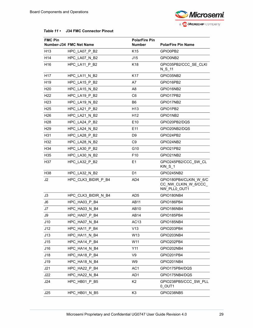
4.9.6 FMC Connector - HPC (J34)The PolarFire GPIO, XCVR1, and XCVR3 signals are routed to the FMC connector (J34) for application development.
The following table provides the J34 FMC pinout details.
Table 11 • J34 FMC Connector Pinout
FMC Pin Number-J34 FMC Net Name
PolarFire Pin Number PolarFire Pin Name
A2 HPC_SERDES_1_RX1_P P29 XCVR_1_RX1_P
A3 HPC_SERDES_1_RX1_N P30 XCVR_1_RX1_N
A6 HPC_SERDES_1_RX2_P R31 XCVR_1_RX2_P
A7 HPC_SERDES_1_RX2_N R32 XCVR_1_RX2_N
A10 HPC_SERDES_1_RX3_P T29 XCVR_1_RX3_P
A11 HPC_SERDES_1_RX3_N T30 XCVR_1_RX3_N
A14 HPC_SERDES_3_RX0_P G31 XCVR_3_RX0_P
A15 HPC_SERDES_3_RX0_N G32 XCVR_3_RX0_N
PolarFire
1.8 V
DIP1
DIP2
DIP3
DIP4
DIP5
DIP6
DIP7
DIP8
4.7
K
4.7
K
SW11
0
1
Microsemi Proprietary and Confidential UG0747 User Guide Revision 4.0 24

Board Components and Operations
A18 HPC_SERDES_3_RX1_P J31 XCVR_3_RX1_P
A19 HPC_SERDES_3_RX1_N J32 XCVR_3_RX1_N
A22 HPC_SERDES_1_TX1_P P33 XCVR_1_TX1_P
A23 HPC_SERDES_1_TX1_N P34 XCVR_1_TX1_N
A26 HPC_SERDES_1_TX2_P T33 XCVR_1_TX2_P
A27 HPC_SERDES_1_TX2_N T34 XCVR_1_TX2_N
A30 HPC_SERDES_1_TX3_P U31 XCVR_1_TX3_P
A31 HPC_SERDES_1_TX3_N U32 XCVR_1_TX3_N
A34 HPC_SERDES_3_TX0_P F33 XCVR_3_TX0_P
A35 HPC_SERDES_3_TX0_N F34 XCVR_3_TX0_N
A38 HPC_SERDES_3_TX1_P H33 XCVR_3_TX1_P
A39 HPC_SERDES_3_TX1_N H34 XCVR_3_TX1_N
B1 HPC_CLK_DIR_B6 D19 HSIO42PB6
B4 HPC_DP9_M2C_P L27 XCVR_1C_REFCLK_P
B5 HPC_DP9_M2C_N L28 XCVR_1C_REFCLK_N
B8 HPC_DP8_M2C_P R27 XCVR_1B_REFCLK_P
B9 HPC_DP8_M2C_N R28 XCVR_1B_REFCLK_N
B12 HPC_SERDES_3_RX3_P L31 XCVR_3_RX3_P
B13 HPC_SERDES_3_RX3_N L32 XCVR_3_RX3_N
B16 HPC_SERDES_3_RX2_P K29 XCVR_3_RX2_P
B17 HPC_SERDES_3_RX2_N K30 XCVR_3_RX2_N
B20 HPC_SERDES_3_INT_REFCLK_P J27 XCVR_3A_REFCLK_P
B21 HPC_SERDES_3_INT_REFCLK_N J28 XCVR_3A_REFCLK_N
B28 HPC_DP8_C2M_P H29 XCVR_3C_REFCLK_P
B29 HPC_DP8_C2M_N H30 XCVR_3C_REFCLK_N
B32 HPC_SERDES_3_TX3_P M33 XCVR_3_TX3_P
B33 HPC_SERDES_3_TX3_N M34 XCVR_3_TX3_N
B36 HPC_SERDES_3_TX2_P K33 XCVR_3_TX2_P
B37 HPC_SERDES_3_TX2_N K34 XCVR_3_TX2_N
C2 HPC_SERDES_1_TX0_P N31 XCVR_1_TX0_P
C3 HPC_SERDES_1_TX0_N N32 XCVR_1_TX0_N
C6 HPC_SERDES_1_RX0_P M29 XCVR_1_RX0_P
C7 HPC_SERDES_1_RX0_N M30 XCVR_1_RX0_N
C10 HPC_LA06_P_B2 G15 GPIO5PB2
C11 HPC_LA06_N_B2 G16 GPIO5NB2
C14 HPC_LA10_P_B2 J16 GPIO31PB2
C15 HPC_LA10_N_B2 K16 GPIO31NB2
Table 11 • J34 FMC Connector Pinout
FMC Pin Number-J34 FMC Net Name
PolarFire Pin Number PolarFire Pin Name
Microsemi Proprietary and Confidential UG0747 User Guide Revision 4.0 25

Board Components and Operations
C18 HPC_LA14_P_B2 F13 GPIO22PB2
C19 HPC_LA14_N_B2 E13 GPIO22NB2
C22 HPC_LA18_CC_P_B2 G5 GPIO11PB2/CLKIN_S_7
C23 HPC_LA18_CC_N_B2 F5 GPIO11NB2
C26 HPC_LA27_P_B2 E6 GPIO13PB2
C27 HPC_LA27_N_B2 D6 GPIO13NB2
C30 HPC_SCL_B4 V12 GPIO205PB4/DQS
C31 HPC_SDA_B4 V11 GPIO205NB4/DQS
D4 HPC_SERDES_1_INT_REFCLK_P N27 XCVR_1A_REFCLK_P
D5 HPC_SERDES_1_INT_REFCLK_N N28 XCVR_1A_REFCLK_N
D8 HPC_LA01_CC_P_B2 G9 GPIO6PB2/CLKIN_S_4
D9 HPC_LA01_CC_N_B2 F9 GPIO6NB2
D11 HPC_LA05_P_B2 F14 GPIO19PB2
D12 HPC_LA05_N_B2 F15 GPIO19NB2
D14 HPC_LA09_P_B2 L17 GPIO30PB2
D15 HPC_LA09_N_B2 M17 GPIO30NB2
D17 HPC_LA13_P_B2 H14 GPIO3PB2
D18 HPC_LA13_N_B2 G14 GPIO3NB2
D20 HPC_LA17_CC_P_B2 F8 GPIO9PB2/CLKIN_S_6
D21 HPC_LA17_CC_N_B2 F7 GPIO9NB2
D23 HPC_LA23_P_B2 C7 GPIO12PB2
D24 HPC_LA23_N_B2 B7 GPIO12NB2
D26 HPC_LA26_P_B2 G12 GPIO18PB2
D27 HPC_LA26_N_B2 G11 GPIO18NB2
D29 HPC_TCK
D30 HPC_TDI
D31 HPC_TDO
D33 HPC_TMS
D34 HPC_TRST_L
E2 HPC_HA01_CC_P_B4 V3 GPIO208PB4
E3 HPC_HA01_CC_N_B4 V4 GPIO208NB4
E6 HPC_HA05_P_B4 AB12 GPIO187PB4/DQS
E7 HPC_HA05_N_B4 AA12 GPIO187NB4/DQS
E9 HPC_HA09_P_B4 T5 GPIO217PB4/DQS
E10 HPC_HA09_N_B4 T4 GPIO217NB4/DQS
E12 HPC_HA13_P_B4 AB5 GPIO182PB4
E13 HPC_HA13_N_B4 AC4 GPIO182NB4
Table 11 • J34 FMC Connector Pinout
FMC Pin Number-J34 FMC Net Name
PolarFire Pin Number PolarFire Pin Name
Microsemi Proprietary and Confidential UG0747 User Guide Revision 4.0 26

Board Components and Operations
E15 HPC_HA16_P_B4 W8 GPIO199PB4/DQS
E16 HPC_HA16_N_B4 Y8 GPIO199NB4/DQS
E18 HPC_HA20_P_B4 W6 GPIO197PB4
E19 HPC_HA20_N_B4 Y6 GPIO197NB4
E21 HPC_HB03_P_B5 J6 GPIO235PB5/DQS
E22 HPC_HB03_N_B5 J5 GPIO235NB5/DQS
E24 HPC_HB05_P_B5 L8 GPIO236PB5
E25 HPC_HB05_N_B5 L7 GPIO236NB5
E27 HPC_HB09_P_B5 J8 GPIO237PB5
E28 HPC_HB09_N_B5 K8 GPIO237NB5
E30 HPC_HB13_P_B5 M2 GPIO221PB5
E31 HPC_HB13_N_B5 M1 GPIO221NB5
E33 HPC_HB19_P_B5 N8 GPIO231PB5
E34 HPC_HB19_N_B5 M7 GPIO231NB5
E36 HPC_HB21_P_B5 M6 GPIO234PB5
E37 HPC_HB21_N_B5 M5 GPIO234NB5
F1 HPC_PG_M2C_B6 C19 HSIO45NB6
F4 HPC_HA00_CC_P_B4 W5 GPIO195PB4
F5 HPC_HA00_CC_N_B4 Y5 GPIO195NB4
F7 HPC_HA04_P_B4 AB9 GPIO183PB4
F8 HPC_HA04_N_B4 AA8 GPIO183NB4
F10 HPC_HA08_P_B4 AB7 GPIO179PB4
F11 HPC_HA08_N_B4 AB6 GPIO179NB4
F13 HPC_HA12_P_B4 T7 GPIO218PB4
F14 HPC_HA12_N_B4 U7 GPIO218NB4
F16 HPC_HA15_P_B4 V8 GPIO198PB4
F17 HPC_HA15_N_B4 V7 GPIO198NB4
F19 HPC_HA19_P_B4 AB4 GPIO177PB4
F20 HPC_HA19_N_B4 AC3 GPIO177NB4
F22 HPC_HB02_P_B5 L4 GPIO225PB5
F23 HPC_HB02_N_B5 M4 GPIO225NB5
F25 HPC_HB04_P_B5 P9 GPIO230PB5
F26 HPC_HB04_N_B5 P8 GPIO230NB5
F28 HPC_HB08_P_B5 L3 GPIO223PB5/DQS
F29 HPC_HB08_N_B5 L2 GPIO223NB5/DQS
F31 HPC_HB12_P_B5 N4 GPIO224PB5
F32 HPC_HB12_N_B5 N3 GPIO224NB5
Table 11 • J34 FMC Connector Pinout
FMC Pin Number-J34 FMC Net Name
PolarFire Pin Number PolarFire Pin Name
Microsemi Proprietary and Confidential UG0747 User Guide Revision 4.0 27

Board Components and Operations
F34 HPC_HB16_P_B5 K5 GPIO232PB5
F35 HPC_HB16_N_B5 L5 GPIO232NB5
F37 HPC_HB20_P_B5 N7 GPIO228PB5
F38 HPC_HB20_N_B5 N6 GPIO228NB5
G2 HPC_CLK1_M2C_P_B2 C11 GPIO29PB2/CLKIN_S_9/CCC_SE_CLKIN_S_9
G3 HPC_CLK1_M2C_N_B2 B11 GPIO29NB2
G6 HPC_LA00_CC_P_B2 H9 GPIO7PB2/CLKIN_S_5
G7 HPC_LA00_CC_N_B2 H8 GPIO7NB2
G9 HPC_LA03_P_B2 H16 GPIO32PB2/DQS
G10 HPC_LA03_N_B2 H17 GPIO32NB2/DQS
G12 HPC_LA08_P_B2 J14 GPIO2PB2/DQS
G13 HPC_LA08_N_B2 J13 GPIO2NB2/DQS
G15 HPC_LA12_P_B2 F12 GPIO23PB2
G16 HPC_LA12_N_B2 E12 GPIO23NB2
G18 HPC_LA16_P_B2 D10 GPIO26PB2/DQS
G19 HPC_LA16_N_B2 D11 GPIO26NB2/DQS
G21 HPC_LA20_P_B2 B9 GPIO25PB2
G22 HPC_LA20_N_B2 A9 GPIO25NB2
G24 HPC_LA22_P_B2 D8 GPIO14PB2/DQS
G25 HPC_LA22_N_B2 C8 GPIO14NB2/DQS
G27 HPC_LA25_P_B2 J11 GPIO4PB2
G28 HPC_LA25_N_B2 H11 GPIO4NB2
G30 HPC_LA29_P_B2 B10 GPIO28PB2
G31 HPC_LA29_N_B2 A10 GPIO28NB2
G33 HPC_LA31_P_B2 E7 GPIO15PB2
G34 HPC_LA31_N_B2 E8 GPIO15NB2
G36 HPC_LA33_P_B2 H7 GPIO8PB2/DQS
G37 HPC_LA33_N_B2 G7 GPIO8NB2/DQS
H2 HPC_PRSNT_M2CL_B6 D20 HSIO42NB6
H4 HPC_CLK0_M2C_P_B2 D13 GPIO27PB2/CLKIN_S_8/CCC_SE_CLKIN_S_8
H5 HPC_CLK0_M2C_N_B2 C12 GPIO27NB2
H7 HPC_LA02_P_B2 L19 GPIO34PB2
H8 HPC_LA02_N_B2 L18 GPIO34NB2
H10 HPC_LA04_P_B2 J18 GPIO33PB2/CCC_SE_CLKIN_S_10
H11 HPC_LA04_N_B2 J19 GPIO33NB2
Table 11 • J34 FMC Connector Pinout
FMC Pin Number-J34 FMC Net Name
PolarFire Pin Number PolarFire Pin Name
Microsemi Proprietary and Confidential UG0747 User Guide Revision 4.0 28
Board Components and Operations
H13 HPC_LA07_P_B2 K15 GPIO0PB2
H14 HPC_LA07_N_B2 J15 GPIO0NB2
H16 HPC_LA11_P_B2 K18 GPIO35PB2/CCC_SE_CLKIN_S_11
H17 HPC_LA11_N_B2 K17 GPIO35NB2
H19 HPC_LA15_P_B2 A7 GPIO16PB2
H20 HPC_LA15_N_B2 A8 GPIO16NB2
H22 HPC_LA19_P_B2 C6 GPIO17PB2
H23 HPC_LA19_N_B2 B6 GPIO17NB2
H25 HPC_LA21_P_B2 H13 GPIO1PB2
H26 HPC_LA21_N_B2 H12 GPIO1NB2
H28 HPC_LA24_P_B2 E10 GPIO20PB2/DQS
H29 HPC_LA24_N_B2 E11 GPIO20NB2/DQS
H31 HPC_LA28_P_B2 D9 GPIO24PB2
H32 HPC_LA28_N_B2 C9 GPIO24NB2
H34 HPC_LA30_P_B2 G10 GPIO21PB2
H35 HPC_LA30_N_B2 F10 GPIO21NB2
H37 HPC_LA32_P_B2 E1 GPIO245PB2/CCC_SW_CLKIN_S_1
H38 HPC_LA32_N_B2 D1 GPIO245NB2
J2 HPC_CLK3_BIDIR_P_B4 AD4 GPIO180PB4/CLKIN_W_6/CCC_NW_CLKIN_W_6/CCC_NW_PLL0_OUT1
J3 HPC_CLK3_BIDIR_N_B4 AD5 GPIO180NB4
J6 HPC_HA03_P_B4 AB11 GPIO186PB4
J7 HPC_HA03_N_B4 AB10 GPIO186NB4
J9 HPC_HA07_P_B4 AB14 GPIO185PB4
J10 HPC_HA07_N_B4 AC13 GPIO185NB4
J12 HPC_HA11_P_B4 V13 GPIO203PB4
J13 HPC_HA11_N_B4 W13 GPIO203NB4
J15 HPC_HA14_P_B4 W11 GPIO202PB4
J16 HPC_HA14_N_B4 Y11 GPIO202NB4
J18 HPC_HA18_P_B4 V9 GPIO201PB4
J19 HPC_HA18_N_B4 W9 GPIO201NB4
J21 HPC_HA22_P_B4 AC1 GPIO175PB4/DQS
J22 HPC_HA22_N_B4 AD1 GPIO175NB4/DQS
J24 HPC_HB01_P_B5 K2 GPIO238PB5/CCC_SW_PLL0_OUT1
J25 HPC_HB01_N_B5 K3 GPIO238NB5
Table 11 • J34 FMC Connector Pinout
FMC Pin Number-J34 FMC Net Name
PolarFire Pin Number PolarFire Pin Name
Microsemi Proprietary and Confidential UG0747 User Guide Revision 4.0 29

Board Components and Operations
J27 HPC_HB07_P_B5 K7 GPIO233PB5
J28 HPC_HB07_P_B5 K6 GPIO233NB5
J30 HPC_HB11_P_B5 N2 GPIO220PB5
J31 HPC_HB11_N_B5 N1 GPIO220NB5
J33 HPC_HB15_P_B5 P4 GPIO222PB5
J34 HPC_HB15_N_B5 P3 GPIO222NB5
J36 HPC_HB18_P_B5 R7 GPIO226PB5
J37 HPC_HB18_N_B5 R8 GPIO226NB5
K4 HPC_CLK2_BIDIR_P_B4 AC2 GPIO174PB4/CLKIN_W_7/CCC_NW_CLKIN_W_7/CCC_NW_PLL0_OUT0
K5 HPC_CLK2_BIDIR_N_B4 AD3 GPIO174NB4
K7 HPC_HA02_P_B4 AC7 GPIO178PB4
K8 HPC_HA02_N_B4 AC6 GPIO178NB4
K10 HPC_HA06_P_B4 AC9 GPIO181PB4/DQS/CCC_NW_PLL0_OUT0
K11 HPC_HA06_N_B4 AC8 GPIO181NB4/DQS
K13 HPC_HA10_P_B4 AC11 GPIO184PB4
K14 HPC_HA10_N_B4 AC12 GPIO184NB4
K16 HPC_HA17_CC_P_B4 T9 GPIO219PB4/CLKIN_W_3/CCC_SW_CLKIN_W_3
K17 HPC_HA17_CC_N_B4 T8 GPIO219NB4
K19 HPC_HA21_P_B4 W10 GPIO200PB4
K20 HPC_HA21_N_B4 Y10 GPIO200NB4
K22 HPC_HA23_P_B4 AB2 GPIO176PB4
K23 HPC_HA23_N_B4 AB1 GPIO176NB4
K25 HPC_HB00_CC_P_B5 G2 GPIO243PB5/CLKIN_W_0/CCC_SW_CLKIN_W_0
K26 HPC_HB00_CC_N_B5 G1 GPIO243NB5
K28 HPC_HB06_CC_P_B5 H2 GPIO240PB5/CLKIN_W_1/CCC_SW_CLKIN_W_1
K29 HPC_HB06_CC_P_B5 H1 GPIO240NB5
K31 HPC_HB10_P_B5 P6 GPIO229PB5/DQS
K32 HPC_HB10_N_B5 P5 GPIO229NB5/DQS
K34 HPC_HB14_P_B5 R5 GPIO227PB5
K35 HPC_HB14_N_B5 R6 GPIO227NB5
K37 HPC_HB17_CC_P_B5 J1 GPIO239PB5/CLKIN_W_2/CCC_SW_CLKIN_W_2/CCC_SW_PLL0_OUT0
K38 HPC_HB17_CC_N_B5 K1 GPIO239NB5
Table 11 • J34 FMC Connector Pinout
FMC Pin Number-J34 FMC Net Name
PolarFire Pin Number PolarFire Pin Name
Microsemi Proprietary and Confidential UG0747 User Guide Revision 4.0 30

Pin List
Microsemi Proprietary and Confidential UG0747 User Guide Revision 4.0 31
5 Pin List
For information on all of the package pins on the PolarFire device, see Package Pin Assignment Table.

Board Component Placement
Microsemi Proprietary and Confidential UG0747 User Guide Revision 4.0 32
6 Board Component Placement
The following figure shows the placement of various components on the PolarFire Evaluation Board silkscreen.
Figure 18 • Silkscreen Top View
The following figure shows the bottom view of the PolarFire Evaluation Board silkscreen.
Figure 19 • Silkscreen Bottom View
SW5
L7
U20
C64
R91
C60U13
VDD_EN
U59
TP127R255 C1
73U53
R240
TP12
2
TP121
R212
R201
R205
DS19
GAUX
1
R127
R121
R131
R84
R264C183
Q9
U56TP
126
C140
U45
SW4
SW6
C83
C80 U21
R115C71
C72
R112
U14
R104
J23
DS26
TP33
R120R98
R111
R95R94
R107
R92C37C35R8
8DS
15
R336
R216
R506
DS25
J16
L6
Y3
C62
R97R
90R9
6
C59
R89
R52
DS24
TP-AGND1
SW7
C828
C123
3
J28
J20
TP50
R155
TP38
R146
R144R141
TP24
TP25
C54C3
3R7
2
R348
Q13
TP124
J32
C117
R165 J21
U27
C61 C55 C56
C18
C19
C17
Y2
R49
R47R4
0
C171
SW11
SW8
U38
J27
J22
C42
C41
C43
C40C3
9C3
4
C22C20
C21
TP10
DS23
R41
Q2
R253
C172
U54
SW9
C119 C116
R186
R185
J18
R180
R181
R178
C48
C47
C46
C44
C45
R83
C32R8
2R7
3 C23
TP-5
V1
J5
C8
C169
L11
U39
J227
J19
C52
C50
C51
C49
R81
R87CR
1
R251
R237
C170
SW10
R2562
C118 J29
J26
U35
BD3
TP-1
.5V1
BD2
J14
C74
C66C65
C68
TP20
C53
C26
R252
R238
C669R208U44
R204TP114
TP108
R187
U33R184
BD4
BD1
U29
U17
BD0
C38
CR2 TP7
TP4
TP2
TP1
3P3_
EN
U57
TP12
5
R594
R164
C76
TP21
J9
R269C185
R279
R267
J34
TP-3.3V1
R188
U34
X1
J48
J45
R161TP37
R156
TP31
C77
D1
TP12
9TP
43
J17
TP35
TP28TP32
U22
U11
R51
SW3
U15
J4
TP-GND1
12_E
N
U55
R236
R235
C163
TP11
9
J35
TP15
J13
R270
C178
DS21
DS27
R53
DS3
R29
R28
R275
TP131
VDDA_ENU60
R230
D9
DS5
DS4
R30
R31
R280C186
R258
C180
R249
R245
D11
J30
J15
R55R54
DS6
DS7
R32
J46
C175
C176
R271R276
R256
0R2
561
TP123
J39
DS20
DS22
TP57
R56 R57
DS9
DS8
R34
R33
R282
R281
R242
U50
J36
TP11
1
TP11
0
U40
TP66
TP65
TP53
U26
U12
R58
DS11
DS10
R35
R36
R283
U58
Y4
R243
TP11
2TP
113
TP68
TP67
TP60
TP44
DS18
C36
R60R59
R70
DS17
DS12
R37
R38
R284R278R277
R274
R261
C166
TP61
TP56
TP48
TP47
TP46
R105
R61
R62DS
14
DS13
R39
Y6
R262
Y5
R244
C160
U51
TP10
3TP
102
TP96
TP95
TP10
1
TP51
TP52
DS16
R287
J47
R260
C167
L10
TP118
L8
U37
C84
C91
TP27
R289
R288
C181
R263
R256
R254
C158
D10
R64R65R66
R68R67
C7C13
C126
C122C120
R194R196
R159
R157
R158
L5
TP23
U7
R290
C182
C177
U52
C12
C14
U10
L3
C127
Q3
R193
C92
TP34
C85
C82
R137
R285
R259
Q8R2
31R229
C25
R44
R45 C11
R199
R198
C102
1V_ENC99
L4
TP18
R71
R48
R42
R27
R247
D8
Q4
U6
TP8
R200R202
R197
J25C105
C104
R138
J6TP3
5V_E
N
CON3
C168
C164
R233
R232
TP12
0
1P5V_EN_TP_SMD
R118
TP22
C30C28C27
R207C31C29
U41
TP11
5
R220
C136
C139
R145
C81
U25
U28
U24
R286
C162
C161
TP134
TP135
R221
R215
R219
R210
R203
R206
R195 C130
C134
U46
R213
R154
R192
R150
C89
R140
C86
C79C78
J37
C280
LED10
LED11
LED9
LED7
LED8
LED5
LED6
C132
LED4
TP10
9C1
29
R211 TP132
U42
U30
J41
C270
C278
C289
L9
J7
R424
C265
C75U18
U19
R225
R226
U49
R222
TP133
R163
TP19
R160
R432
C154
C156
C155
C422Q20
GAUX_EN1
U47
J12
J42
R471
TP26
C383
C372U68
R463
R457
C123
R209
R108
R109 C58
R100
R101
C57
J38
C157
R223
R458R189
C335
U32
R454TP49
C113DPR2
R110R106
R102
R103
C142C141
C143
C110
R183
C124
R162
C114
DPR1
U48
TP16
L2
Q1
C153C144
R191
R190
C111
C103
C101
U36
C24
C15
C9
U5
C6
C151
C152 C145
C146
C109
1_PP
S_OU
TBI
TS_O
UTC1
6
TP14TP17
R69
R50
C10R63
R43
C108
R129R130R134R136C1
00
U23
R124
R114R119
R122R116R113
R125
R93TP13
TP11 U8
J10J2
26
SW2
TP128
C147
C148
C94
C107C106
U16
R85U9
J11J2
25
J40
C149
C150
TP62
C95 C96
R142
C93C90
R86 R7
5R7
6TP9
R46
TP6TP5
U4
J44
C159
U31
U43
C97
R149R143
R153
R77
R78
R80
R79
Q11
Q10
Q7
Q6
TP45C98
TP36
TP12
R268
R246
R234
R151R147
R133
R139 R135
C87
R132
TP30
R128R126
C69
SYNC
E_OU
T
R117R123
R272
R265
R257
C135
J33
C125
C121
C115
C830
C112
R152R148
C88
C70
C73
C63
GAUX_EN
R74
R99
J8
C184
TP130
R273
R266C179
J43
R250
C174R248
R239
C165
R241
C131
C137
1
2
A1
A40
K1
K40
1
AA1
1 A
5
BB1
9
10
1
3
12
BB1
1
2
16
AA1
BB1
A
B A
A1B1
ONOF
F
B
B1
78
AA1
A
A1
B
B1
56
B
34
AA1B1
A
1
A
34
1
A1
1
A
AP
A1
A1
I1
V1
N
N
I2
V2
A1
A
9
1
9
1
AA1
2
9 10
3
2
3
2
A1
I1
V2V1
B32
20B1
1 A
B12
B11
I2
10
11
21
87
217 8
R1 J3
E
1P8V_ZL
12
J4
VDDA
UX_G
PIO
TP126_VDD_REG_CS
XCVR
_VRE
F
GND
GND
GND
USER RST
E2
2019
3P3V_SF
K22
F5
DEVRST#VDDAUX5
K1
E 1P5V
_SF
B27
K2D14
D15
VDD_
USB_
F2
GND
TP124_1P8V
C21
TCK TDO
A25
TMS
VDD25 TRST
F25
TDI
GND
C22
B21
G20
F24
B19
JTAG
- P
ROG
H23
D21
H24
SW11
SPI- PROG
Mini
USB
3P3V
GND
SCL
SDA
GND
12V
I/P
GND
VCCIO_VADJ
VCCIO_FMC
TCK
TD0
SW
FMC-HPC CONN
RMT
TP35_TDITP28_TMSTP31_TRST
OFF
ON
PRB_
APR
B_B
REFCLKP
REFCLKN
D
GND
K4K3
TP11_GND
GND
RJ45 - PORT 1
RJ45 - PORT 0
GND
GND
TCK
G1
H1
FABRIC JTAGTMSTDO
3P3V TRST
GND
TX-DISABLE
DS3_
VDD_
REG
DS4_
1P5V
_REG
TDI
L
VDDA_REG
H2
G2
DS5_
0P75
V_VT
T_DD
R3DS
6_1P
2V_R
EGGN
D
H
125
MHz
12P0
V3P
3V
SFP+ CONN
DS9_
1P0V
_PHY
DS8_
1P8V
DS7_
0P6V
_VTT
_DDR
4
5P0V
122.
88MH
z15
6.25
MHz
B
DS10
_VDD
A_RE
G
DS13
_VCC
IO_H
PC_V
ADJ
DS12
_VDD
25DS
11_V
DDAU
X_GP
IO
WAKE#
GND
DS14
_VDD
AUX5
1P0V_PHY
K16
5P0V
B 0P75V_VTT_DDR3
TP11
5.1P
2V_R
EG
TMS
TDO
TRST
TDITCK
GND
VDD2
5
1P5V_REG
TDI TDO
TRSTTCK
TMS
GND
POLARFIRE_EVAL_KIT_REV-C
RX0P
H21
H22
F23
C27
D25
C26
B26
F22
1P2V_REG
C4 D3 D4
A2 A3
TX0P
DVP-102-000481-001
C3
1P2V
_REG
_CS
GND
TX0N
VDD25_DUT_CS_N5_F2
D
3.3V2.5V1.8V1.5V1.2V
RX0N
VCCIO_HPC_VADJ
VDDA
25_R
5_F2
TP13_3P3V_ZL
C297
Q22
R2498
U90
R2558R584R582
C521
C452
C409R473
C398C389
C369
C337L16
R445
C318C308
R669
C520
C463
R472
R448
R449
R440R435
D14
R358
C519
C435C414
Q18
C321
R438
R433
R408
R365R394
R331
R323
R650
R651
R647
C518
C218
R330
R648
R649
R362
Q14
R364
C224
FB5
C223
C200
C212
R317R313
C570
C577
C548
C571
C535
C508
R518
C478
R478
C436
C394
C387C395
FB8
C326C3
14
C310
C288
C293C275
C256C259
FB4
C211
C194C198
C803
C802
R561C576
R558
C557
C512
C534
C457
C501
C392
C393
C325
C357
C287
C257
FB2 FB3
L13
C203
C213
R664
R662R661
R663
C778
C754C756
C732 C738
R583C615C644 C6
70
C586C609
C567
R562C555
C524C522
C481
C725C715
C737
C703C713
C676
C693 C694C684C6
75
C390
C643C677
C635
C324
C323C591
C606
C309C300
R409R425
FB1
R642R643R644
R640
C775
C723
C764C750
R598
C678C7
58C6
87
C695
C733
C575
C569
C601
C582C540
C509
C736
C740
C735
C699
C708 C6
98
C700
C739
R586
C692
C672
C674
C673
C655
C637
C654
C656
C632
C590
C624
C589
C626
C614 C603
C596
C299
C298U67
R367C244
U66 L12
C826
Y9 C688
C753
C752
C724C743C7
27
C580
C533
C744 C734
C711
C716
C742
C707
C728
C697
C671
C680
C689
C662
C696
C639
C652
C634
C653
C612
C593
C610
C611
C613
R419
R412
R391
R339
C205R327
R604
C665
C625
C551
C516
C467R529
C714
C710
C706
C679
C691
C661
C683C702
C660
C636
C664
C631
C638
C642
C597
R571
C622 C608C602
C623
C245R354
Q15
R333
C209
R656
R655R654
C705
R591
R557
R566
R540R503
R456
Q16
C252
R393
R352
R326 U65
R328
C817
C627
R578Q19
U70
C538
C476
U69
R447
R464
R455
R398R403R411
C215
C227
C199 R322
R676
R672
R639
R638
C719
R606R599
C686
C712
R577R2559
C553R554
C464
R553
C469
R255
7 R510
R501
C373
C379
C366C370
C355
C362
C346
C345
C361
C255
R388C246
C249C207
R338
R320
R679
C814
C811
R637
R636
C667 C682
U76R5
72
R684
R481 R482
R466
C377
C375
C374
C376
C358
C341
C344
C343
C342
C363
C360
C359
C206
C214R337
R319
Q24
C813C810
R635
R633
U81
C562
R536
U92
C123
2C3
82
C402
C354C339C338
FB7
R357
C232
R347C210
C202
D13
R675R667
R634R632
C721
R608R601
U75
R573
R508
R498
R496
R495
C388
C371
C320
C277
R346
R344
R345
R343
C208
C201
R324
C197
C193
C820
R659
C821
C666
R565
U72
R534
R494
R493
R492
C403
C385
R451
C333
C332
C334
R380
R379
R381
C274
C273
R342R361
C217R325
R671
C809 C807
C720
R607R600
C628
C565C561
R505
R479 R491
R490
R470
C380
R450R446C291
R376
R377
R375
R374
R378
C276
R350 C222
C219
F1
R674
R665
C815
C806
R588
R569
U71
R507
R576
C396
C397
C412
C378
L15 C356
C365
C285
C313
C331
R372
R371
R373
R370
C290C286
R360
C237
Q23
R641
C722
R609R603
U74
R574
C563
C466
R519
C413
C450
L18
R459
R417C279
R443
R368
R369R410
R359
C233
C235
C236
C204
R678
R668
C816
C1229
C651
C650
R547
R531
C451
C408
C381
C351
C315 C829
FB6
C271R685
D15
R353
C234
C819
C1228
C461
C433
C391
L17
C319
R657
C690
C432
R335
R658
R597
R590
C507
R528R526
R542R543
C496C504
R545R522
R527
R523
R521R544
C500
R525R524 C505
C506
C216
U63
Q21
R596
R589
R511
R513R512
R515R514
R516R517
R334R341
C812
C808
R619R618
R622
R616R614R613R612R611R610
C495
C417C416
R484R485
C420C419
C418
R487
R486
R488
C272
C243
U62
C823
C822
C800
R621
R568
R579
R552
R559
R468
R461
R452
R441
C825
C818
C805
R631
C793
R620
C786
R546
R550
C498C493
C474
C460
C479
C424
C437
C426
C425
R476
C824
C804
R627
R626
C801
C788
C790
C581
C600
C559
C531
R549
C510
C489
C490
C491
C492
C448
C445
C447
C427C421
C446
C384
C364
C336
C304
R355
R356
U61R6
29R6
30R6
25C4
87C4
86C4
85
C488
C473C470
C459
R497R483 R4
80
C442
C441
C440
C429
C443
C444
R477
C220
R682
C751
L20
R556
C530
C503
C513
C480
C458
R489C428
C439
C449
C352
C367
C221
R683
R673
R660
R387
C241C240C239C238
R385
R314
C629
C630
C574C587
C554
L14
R316
R680
R389
R397
R406
R401
R395
R400
C263
C248
R321
C523
C231
R315Q12
CON3
U79
R653
R645
R386
R420
R431
R414
R428
R413
R418
R426
R430
R437
C296 C283
L19
R467
C368
C353Q17
C230
R681
R399
R390
C67
C303C329
C292
R567R564R560
C532
R548R551
C228
R366R405 C251
R396
R383R382
R384
C566
U73
R218
C526C527
R465
C528C404C405
C407C406C456
C517C415
C462
R416
C269
R415
R407
R402
R421
U78
R555
C138
R581
R520
R530
R537
R539
C453
C484
C477
C499
C260
C284
R434
R429C254
C247
R602
C242
R595
R563
C128
Q5
C471
C475
C465
C431R500
C386
C266
C261
C262
C250
R593
R580
R585
C253R570
R592
R587
C455
C454C434
C472
R499
C438
C430
C468
R509
R504
R502
C282 C268
R422
C295
R224
C264C281
C777
C747C746R605
C718
C726
C748C749
C731
C423
C410C411
C330 C306
C317C316
C349
C328 C305
C348 C312
C302C327
C301
C399
R228
R227
C681
C659
C685
C704
C647
C645C646
C649C648
C350
C782
C755
C729
C763
C347C605
R615
C797C796R617 C6
40
C798C791
C792
C799
R624
C783
C779
C762
C741
C760
C761C745
C717
C547 C546
C789
C776 C784
C787C7
85
C770
C768C769
C772C771
R340R349R351
R332R329
R312
R623
C780
C781
C765
C759
C757
C1234
C621
C588 C767
R541
C619C618C617
R439R442 C620
R318
C774
C730C766
C658
C709C701
C1236
C607
C1237
C579
C598
C536
C560
C529
C583C572
C483
C552
C585
C564
C568C594
R444
C595
R436 C311C294
C196
C773
C663
C599
C657
C616
C539
C511
C502
C401
C400
C537
C542
C541
C544C543
C545
C229
U64
C795
C592
C668C633C604
C641
C584
C550C556
C573C558
C482
C514
C123
5
C340 Y8
C307
R427
C258
R363
C226
C225
C195
R628
C794
R575
C578
C549
C494
C515
C497
C525
Y7
R462
R453
R460
C322
R423C267
R404R392
1122
50 MHz
FUSE
+1(800) 262-1060
MICROSEMI TECHNICAL SUPPORT
24.576 MHz
APR-2017
305-PD-17-0215

Appendix: Running the Demo Design
Microsemi Proprietary and Confidential UG0747 User Guide Revision 4.0 33
7 Appendix: Running the Demo Design
The onboard PolarFire FPGA comes with a programmed design. For more information on running the demo, see DG0755: PolarFire FPGA JESD204B Standalone Interface.

Appendix: Programming PolarFire FPGA Using the On-Board FlashPro5
Microsemi Proprietary and Confidential UG0747 User Guide Revision 4.0 34
8 Appendix: Programming PolarFire FPGA Using the On-Board FlashPro5
The PolarFire Evaluation Board includes onboard FlashPro5 programmer hardware. An external programmer hardware is therefore not required to program the PolarFire device. The device can be programmed using the FlashPro software installed on the host PC.
Follow these steps to program the on-board PolarFire device:
1. Connect the power supply cable to the J9 connector on the board.2. Connect the USB cable from the Host PC to the J5 (FTDI port) on the board.3. Power on the board using the SW3 slide switch.
When the board is successfully set up, the LEDs start glowing.
4. On the host PC, start the FlashPro software.5. Click New Project to create a new project.6. In the New Project window, do the following, and click OK:
• Enter a project name.• Select Single device as the programming mode.
7. Click Configure Device.8. Click Browse, and select the “xxxxxxxxxxxxxx.stp file from the Load Programming File window.
Note: The programming file will be available in a future release.
9. From the View Programmer pane, select the on-board FlashPro5 programmer as shown in the following figure.
Figure 20 • Selecting the On-Board FlashPro5
10. Click Program to program the device.The Programmer List Window in the FlashPro, shows the Programmer Name, Programmer Type, Port, Programmer Status, and the Programmer Enabled information.
11. When the device is programmed successfully, a Run Program PASSED status is displayed.

Appendix: Power Monitoring
9 Appendix: Power Monitoring
The SmartFusion A2F 200 device on the PolarFire Evaluation Board, monitors the voltage and current on different PolarFire power rails. It measures the current for different components and displays the power on the Microsemi PowerMonitor application. PowerMonitor is a Graphical User Interface (GUI) application that runs on the host PC. The power monitoring program on the SmartFusion device measures the total device power without any manual measurements.
The power monitoring program does the following:
• Monitors voltage on all PolarFire power rails.• Measures current and power on the following rails:
• VDD_REG: Power supply for fabric core.• VDDA_REG: Power supply for transceiver and common circuits.• VDDA25: Power supply for transceiver PLLs. This supply is isolated from other power supplies
to keep the noise low and avoid leakage for PCIe, EXT_PLL, and GPSS.• VDD25_DUT: Power supply for corner phase-locked loop (8 PLLs) and secure non-volatile
memory (sNVM). These are tied together at the package level to keep the noise on the stand alone PLLs low.
• Monitors Flash*Freeze power when the PolarFire device is in Flash*Freeze mode.• Powers-up and powers-down the board when pins 2 and 3 of the J4 jumper are closed.• Powers-down the board if voltage threshold violations are observed on a power rail.
The analog computing engine block in the SmartFusion device is configured to measure the voltage and current on the PolarFire power rails. The following figure shows the power monitoring block diagram.
Figure 21 • Power Monitoring Block Diagram
9.1 PrerequisitesBefore installing PowerMonitor, perform the following steps:
1. Download the PowerMonitor application from the following location:http://soc.microsemi.com/download/rsc/?f=polarfire_power_monitor
2. Ensure that Pin 1 and 2 of the J4 Jumper are closed.3. Connect the Mini USB cable from J5 to the host PC.
The LEDs D2 and D3 start blinking when the power monitor program is running on the SmartFusion device. The board will not power ON unless it is connected via USB to the host PC.
4. Connect the power supply to J9 and turn ON the SW3 switch.5. Ensure that the screen resolution of the Host PC is at least 1280×720. The screen resolution can be
set from Control Panel\Appearance and Personalization\Display\Screen Resolution.
6. Ensure that the text size in the display setting of the Host PC is set to either small (100%) or medium (150%). The display size can be set from Control Panel\Appearance and Personalization\Display.
PolarFire EvaluationKit
User Interface Application
Host PC
SmartFusion ACE
PolarFire Power Rails
Enable Signals
USB - UART
Serial Communication
Microsemi Proprietary and Confidential UG0747 User Guide Revision 4.0 35

Appendix: Power Monitoring
9.2 Installing PowerMonitorTo install PowerMonitor:
1. Extract the contents of the polarfire_power_monitor.rar file.2. From POWER_MONITOR_GUI\Installer folder, double-click the setup.exe file.3. Follow the instructions displayed on the installation wizard.
After successful installation, PowerMonitor appears on the Start menu of the host PC desktop.
4. From the Start menu, click PowerMonitor.The COMPort SetUp window opens.
5. Select the highest numbered COM port, and click Connect.
The PowerMonitor GUI appears on the host PC.
9.3 About Microsemi PowerMonitorThe following figure shows the PowerMonitor GUI.
Figure 22 • PowerMonitor GUI
The PowerMonitor GUI has the following panes:
• CurrentMonitor—This pane displays the current and power measured on VDD_REG, VDDA_REG, VDDA25, VDD25_DUT rails. This pane also displays the total device power. The I/Os are excluded.
• VoltageMonitor—This pane displays the present voltage measured on each voltage rail. This pane also displays the maximum and minimum voltage measured on each voltage rail over the time period of the PowerMonitor application.• Voltage Rail Plot—This pane displays the voltage plot of the selected rail as a blue line. The
green and red lines represent the over-voltage (+3%) and under-voltage (-3%) tolerance levels of that rail. After staring the PowerMonitor GUI, the voltage plot takes minimum 5 seconds to plot the samples.
Microsemi Proprietary and Confidential UG0747 User Guide Revision 4.0 36

Appendix: Power Monitoring
Note: For more information about the recommended minimum and maximum operating voltage of each rail, see the “Recommended Operating Conditions” section of DS0141: PolarFire FPGA Datasheet.
The PowerMonitor GUI has the following buttons:
• Graph—Click this button to view the power consumed by VDD_REG, VDDA_REG, VDDA25, and VDD25_DUT rails, and the total device power.
• Pie—Click this button to view the percentage power consumed by VDD_REG, VDDA_REG, VDDA25, and VDD25_DUT rails out of the total device power.
• Show Log—Click this button to view all of the power monitor program actions in a file.• Power—Click this button to power-up or power-down the board when pins 2 and 3 of J4 jumper are
closed.Note: When pins 1 and 2 of J4 jumper are closed, use SW3 switch to power-up or power-down the board.
Microsemi Proprietary and Confidential UG0747 User Guide Revision 4.0 37

Appendix: Performance Data
10 Appendix: Performance Data
This section describes the performance results of MPF300T Evaluation Kit with different SERDES protocols. All of the steps required to set up the test environment are described. The section also provides information about eye diagram and jitter, and how they vary with protocol.
All the measurements are taken on MPF300T Evaluation Kit with 23 GHz Tektronix scope.
The following protocols are considered for evaluating the performance of the MPF300T Evaluation Kit.
1. JESD204BData Rate: 12.5Gbps - Reference Clock 156.25 MHz
2. 10BASE-G KRData Rate: 10.3125Gbps - Reference Clock 156.25 MHz
3. INTERLAKENData Rate: 10.312Gbps - Reference Clock 156.25 MHz
4. CPRIData Rate: 10.137Gbps - Reference Clock 122.88 MHz
10.1 Setup DetailsThe following hardware and settings are used:
• MPF300T-1FCG1152• Transceiver block 0, Lane 2• Dedicated internal reference clock for the transceiver block (156.25 MHz or 122.88 MHz)• LVDS25 I/O standard for reference clock input• 23 GHz Tektronix (DPO72304) scope set to 100G samples/sec for measuring jitter and plotting eye• Clock recovery configurations for scope:
• Method: PLL-Custom BW• PLL Model: Type II• Damping: 700 m
• 1 foot long cable (part# Sucoflex 100 126E) for connecting the TX ports to the scope• On PolarFire Evaluation board, a 2.3 inch long PCB trace exists between the device and TX SMA
connectors.
The following figure provides a pictorial representation of the hardware setup used for the measurement.
Figure 23 • Hardware Setup for Measurement
Note: All measurements are taken with de-embedding the PCB trace.
Microsemi Proprietary and Confidential UG0747 User Guide Revision 4.0 38

Appendix: Performance Data
10.2 JESD204B ResultsThe following driver settings are used for JESD measurements:
• Signal amplitude: 500 mV • De-emphasis: 0 dB• Pattern used: JSPAT (500 bits)• Driver Impedance: 100 Ω• Data Rate: 12.5 Gbps
The following table summarizes the measurements captured by the scope at 12.5 Gbps transmitter data rate and at a BER of 10E-12.
The following figure shows the data eye plotted for the above settings.
Figure 24 • JESD204B Eye Diagram With De-embedding
Table 12 • JESD204B Jitter Measurements1
1. The measurement data is only indicative. The data is measured in typical conditions using 109757 bits. Results vary with different PVT conditions and scope. See the datasheet for the worst case jitter numbers.
PARAMETER Value
Height 462.03 mV
TJ@BER 18.704 ps
Width@BER 61.296 ps
RJ 673.62 fs
DJ 9.27 ps
Microsemi Proprietary and Confidential UG0747 User Guide Revision 4.0 39

Appendix: Performance Data
10.3 10BASE-G KRThe following driver settings are used for 10BASE-G KR measurements:
• Signal amplitude: 1000 mV • De-emphasis: -1 dB• Pattern used: PRBS31• Driver impedance: 180 Ω • Data rate: 10.3125 Gbps
The following table summarizes the measurements captured by the scope at 10.3125 Gbps transmitter data rate and at a BER of 10E-12.
The following figure shows the data Eye plotted for the above settings.
Figure 25 • 10BASE-G KR Data Eye Diagram
Table 13 • 10BASE-G KR Jitter Measurements1
1. The measurement data is only indicative. The data is measured in typical conditions using 38988 bits. Results vary with different PVT conditions and scope. See the datasheet for the worst case jitter numbers.
PARAMETER Values
Height 911.44 mV
TJ@BER 21.31 ps
Width@BER 75.662 ps
RJ 760.57 fs
DJ 10.66 ps
Microsemi Proprietary and Confidential UG0747 User Guide Revision 4.0 40

Appendix: Performance Data
10.4 InterlakenThe following driver settings are used for Interlaken measurements:
• Signal amplitude: 500 mV • De-emphasis: 0 dB• Pattern used: PRBS31• Driver impedance: 100 Ω • Data rate: 10.3125 Gbps
The following table summarizes the measurements captured by the scope at of 10.3125 Gbps transmitter data rate and at a BER of 10E-12.
The following figure shows the data Eye plotted for the above settings.
Figure 26 • Interlaken Data Eye Diagram
Table 14 • Interlaken Jitter Measurements1
1. The measurement data is only indicative. The data is measured in typical conditions using 90550 bits. Results vary with different PVT conditions and scope. See the datasheet for the worst case jitter numbers.
PARAMETER Values
Height 430.13 mV
TJ@BER 20.572 ps
Width@BER 76.396 ps
RJ 930.07 fs
DJ 7.55 ps
Microsemi Proprietary and Confidential UG0747 User Guide Revision 4.0 41

Appendix: Performance Data
10.5 CPRIThe following driver settings are used for CPRI measurements:
• Signal amplitude: 1000 mV • De-emphasis: -1 dB• Pattern used: PRBS31• Driver Impedance: 180Ω • Data Rate: 10.137 Gbps
The following table summarizes the measurements captured by the scope at 10.137 Gbps transmitter data rate and at a BER of 10E-12.
The following figure shows the data Eye plotted for the above settings.
Figure 27 • CPRI Data Eye Diagram
Table 15 • CPRI Jitter Measurements1
1. The measurement data is only indicative. The data is measured in typical conditions using 35719 bits. Results vary with different PVT conditions and scope. See the datasheet for the worst case jitter numbers.
PARAMETER Value
Height 903.58 mV
TJ@BER 26.664 ps
Width@BER 71.98 ps
RJ 1.08 ps
DJ 11.57 ps
Microsemi Proprietary and Confidential UG0747 User Guide Revision 4.0 42

Appendix: Errata
Microsemi Proprietary and Confidential UG0747 User Guide Revision 4.0 43
11 Appendix: Errata
This section contains information about known issues specific to the PolarFire Evaluation Board.
11.1 Errata Descriptions
11.1.1 Hot swapping is not supported on Programming headers J32, J29, PCIe CONN (CON3), SFP+ cage (J36), GPIO headers (J7, J8)This restriction applies to Rev B and C of the board.
11.1.2 The VDDI3 (Bank 3) supply voltage is higher than the Datasheet specificationBank 3 (VDDI3) and all circuits connected to Bank 3 have supply voltage of 3.3 V. User should not use the supply voltage of 3.3 V for Rev B board of Bank 3. This is addressed in the Rev C board.