u -l power platforms for enhancement
TRANSCRIPT

ULTRA-LOW POWER PLATFORMS FOR HUMAN ENHANCEMENT
Jan M. Rabaey Donald O. Pederson Distinguished Prof. University of California at Berkeley Scientific Co-Director BWRC Director FCRP MuSyC Center Energy-Efficient Systems Symposium
Berkeley, November 2011

ULP MicroElectronics for Human Enhancement Extreme miniaturization combined
ultra-low power circutitry pave the way for “nanomorphic” bio-interfaces “The Nanomorphic Cell is a conception of an atomic-level, integrated, self-sustaining microsystem with five main functions: internal energy supply, s e n s i n g , a c t u a t i o n , c o m p u t a t i o n a n d communication” [REF: Wikipedia]
Opportunities: observing living cells in vivo, brain-machine interfaces
Other readings: M. Crighton,
N. Stephenson

BMI - The Instrumentation of Neuroscience
Learning about the operational mechanisms of the brain – Only marginally understood – Potential benefits to humanity hard
to overestimate – Addressing neural impairments – Human enhancement
– Could have huge impact in totally different domains (e.g. neuro-inspired computation)
The Decade of Neuroscience?

BMI- Taking Medical Care to the Next Level
[Sources: National Institutes of Health, Neurology journal]
Deafness (cochlear implant) ~250 million deaf people worldwide,
2/3 in developing countries > 100,000 cochlear implant users
worldwide 22,000 adults and 15,000 children live
in the US Cost: US$ 40-60K
Deep brain stimulation (DBS) Disease: Movement disorders
(Parkinson’s Disease, tremor) Market Size: Millions Approved in 1997 80,000 implants total worldwide Cost: US$ 50,000

BMI for Motor Control Spinal cord injuries/amputees (upper-
limb prosthesis) ○ Estimated population (US) of 200,000 people ○ 11,000 new cases in the US every year
[Lebedev, 2006] [MAL Nicolelis, Nature, 18 January 2001]

The BMI Spectrum
[Schwartz et al. Neuron, 2006]

Towards Integrated BMI Interface Nodes
[Illustration art: Subbu Venkatraman]
ADC LNA
electrodes
DSP
memory
Tx
regulator
clock
* “Michigan” and “Utah” Electrode Arrays shown

Goal of BMI Interfaces: Acquire and Transmit Neural Signals Reliably and Consistently Over Long Lifespans (> 10 Years)
Action Potential spikes 300Hz-10kHz
10µV-1mV
Local Field Potential (LFP) 1Hz-300Hz; 10µV-1mV
volta
ge
time
DC Offset ±50mV
Challenges: Weak signal, Low SNR, High Offset, Mixture of field potentials and action potentials

Why Extreme Miniaturization?
Resolution – observations at the cellular level
Reliability and longevity - Scarring reduces
sensitivity and cause failure
- Maybe addressed by “truly untethered” free-floating nodes
- Need spatial measurement resolutions on the scale of 100 μm
[Pictures courtesy of T. Blanche, UCB]
neuron
electrode

Batteries problems: ○ size ○ replacement
Energy scavenging inside the body a relatively young research area e.g. utilizing body heat (thermoelectric) 0.6 µW / mm2 @ ΔT=5° [Paradiso05] Glucose biofuel cells attractive,
but need improvement (up to 0.7 µW / mm2 today)
(Electro-)Magnetic Powering advantages: ○ energy source sits outside the body
limitations: ○ possible health risks of EM radiation
Miniaturization - It’s All About Energy!
New Scientist, June 2004
impermeable surface
anode
membrane (glucose permeable)
cathode (O2 selective)
Re-
glucose
oxygen
abiotic system

Wireless Power and Size
Specific absorption rate (SAR) sets the limit on external power
Thermal considerations limit power dissipated by implant
Available power drops with size by d4 or more
11
[Rabaey, Mark, et al., DATE 2011]
Power Available at Matched Input Terminal
Ultra Low-Power Design Essential!

Key Concepts of Ultra-Low Power BMI Nodes
Efficiency - Every electron counts Exploit technology scaling Operate at the lowest possible voltages! Rethink computational and communication paradigms Innovate and think out-of-the-box!

Externally applied power limited by health concerns Limit set by Specific Absorption Rate (SAR) 1.6 W / kg averaged over 1 g of tissue (in US)
Segmented transmit loop increases power available to the implant by 47 % (at 500 MHz)
Efficiency: Maximizing Power that can be Applied
[Mark, Bjorninen et al., Biowireless 2011]

Efficiency – Optimization of RX Antenna Size and Frequency
Maximum Achievable Gain vs. Frequency
(shown for a single turn 1 mm x 1 mm implanted antenna)
Simulations (HFSS) match in-vivo measurements

Boosting the Rectifier Efficiency
At 500 MHz for 1mm antenna Max input voltage: 145 mV
Solution: Pulsed power transmission Keeps average SAR while increasing efficiency by 25%

Proof of Concept: 1 mm3 Wirelessly-Powered Node
[Mark, Chen, et al., VLSI 2011]
1 cm of skin, fat, bone
Delivers 26 uW or 8 uW of power (IEEE, FCC)

Riding the Technology Wave?
IMPLANTED SYSTEM
DSP ADC
Neural Amplifiers
Power Supply
Tx Rx
Micro-stim
Power and Area of minimally-invasive devices dominated by analog front-end: – Ultra-low noise – Offset cancelation – Low frequency signal separation
CIN = 5-20pF Eliminate passives
to reduce area
ADC
S/H BPF
Neural Amp
Mux

Technology Scaling a Must!
[R. Muller et al, ISSCC 2011]
A 0.013mm2, 5uW DC Coupled Neural Signal Acquisition IC with 0.5V Supply Digital transistors are
cheap in advanced CMOS processes
Avoid large capacitances by dc-coupling and filtering in digital domain
No high-precision analog components

Scaling the Supply Voltage Digital processing to reduce data rate and improve reliability
Sorted spikes
Colored trajectories Spike trajectories
Back annotate
Feature
x-trac
t
Original spikes
Clustering
Courtesy: Dejan Markovic [UCLA]
Example: Spike extraction

Ultra Low-Voltage Design
[Courtesy: TT. Liu, UCB]
Register Bank
Memory Feature Extraction
Preamble Buffer
Spike Detection
Spike Alignment
74%
• 0.25 μW/channel @ 0.25V • 0.03mm2 in 65nm CMOS
Self-timed implementation reduces leakage and impact of variability at 0.25 V

Innovative Communication Architectures Wireless data transmission at minimal energy/bit and footprint
Take advantage of wireless powering using RFID-style techniques
Increase data rate by using impulse-based modulation
Reflective Impulse Radio: 2 Mbits/sec, 300 fJ/bit, ~0.01 mm2
[Mark, Chen, et al., VLSI 2011]

Putting it all Together – “Neural Dust”
Thousands of “sensing nodes” freely embedded in neo-cortex
Interrogated by array of nodes located on neo-cortex surface
Communicating with and powered by ex-cranial interfaces
[Courtesy: W. Biederman and D. Yeager, UCB]

Exploring Alternatives Routes : μECoG
2006
0.5 mm
2011
[Courtesy: P. Ledochowitsch, R. Muller]

Fabricating μECoG Arrays 1. Carrier wafer cleaning
2. Parylene deposition (~ 9 μm)
3. Metal lift-off (Cr/Au/Pt, 250 nm total)
4. Parylene deposition (~ 1 μm)
5. Photoresist etch mask
6. Parylene etching and resist removal
7. Device release from carrier
Rep
eat f
or e
ach
met
al la
yer
ASICs can be directly ACF bonded to device – providing structural and electrical integrity
μECoG on Macaque motor cortex (48 channels, 0.8 mm pitch)
[Courtesy: P. Ledochowitsch, M. Mabarbiz]
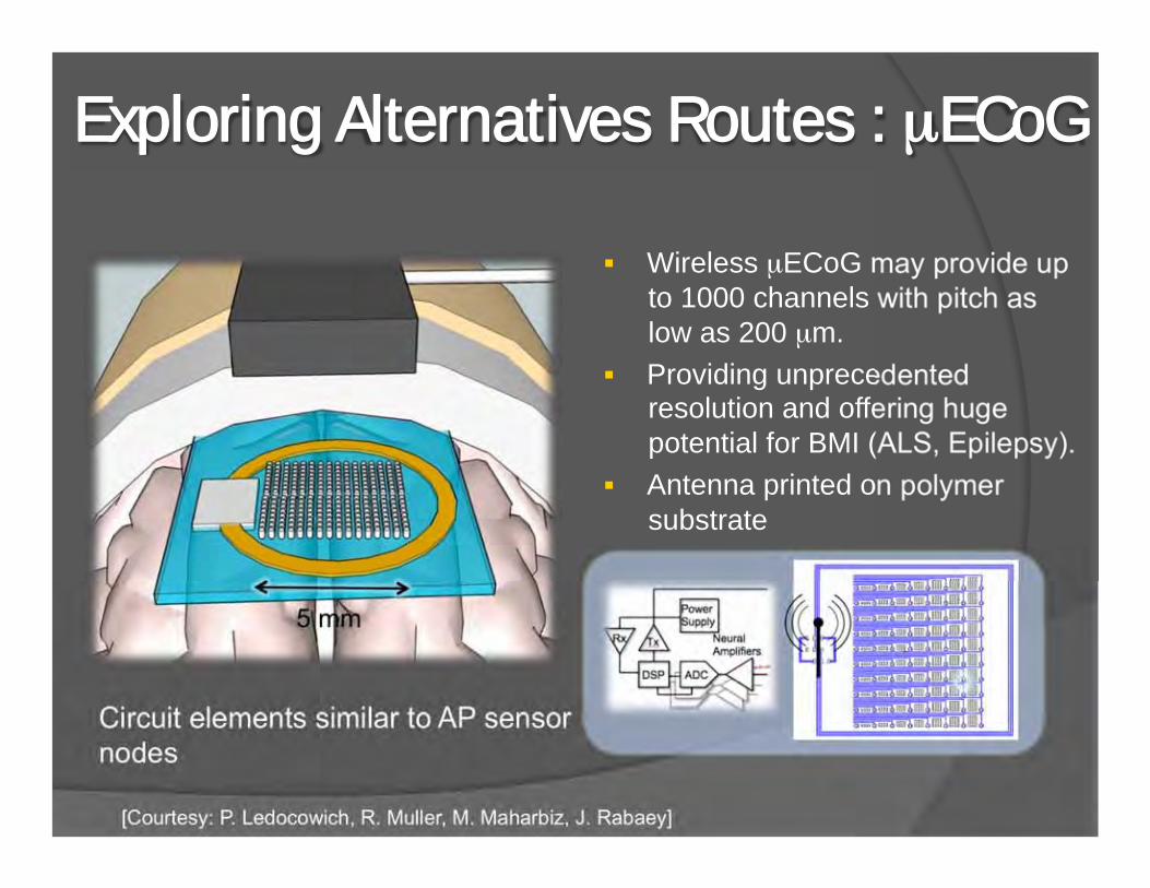
Wireless μECoG may provide up to 1000 channels with pitch as low as 200 μm.
Providing unprecedented resolution and offering huge potential for BMI (ALS, Epilepsy).
Antenna printed on polymer substrate
[Courtesy: P. Ledocowich, R. Muller, M. Maharbiz, J. Rabaey]
Circuit elements similar to AP sensor nodes
5 mm
Exploring Alternatives Routes : μECoG

An Integrated (Long-Term) Vision: Combining “Neural Dust” and μECoG
“An implanted neural interface that can provide imaging of neural activity at multiple scales of resolution using arrays of patterned and free-floating sensors”

Final Reflections …. Brain-Machine Interfaces the ultimate in immersive
technologies - The potential is huge - Societal impact first, human advancement next
ULP circuit and systems design in concert with innovative technologies to provide “cellular electronics”
“It’s the System … Stupid!” - It is not the brain alone - Explore, analyze, and implement advanced
closed-loop learning systems - Interesting signal-processing opportunities
Requires broad multi-disciplinary collaboration - The new reality of engineering - A major attraction to a new generation of
engineers and beyond