two-dimensional electronic transport on the surface of...
TRANSCRIPT
PHYSICAL REVIEW B 86, 235443 (2012)
Two-dimensional electronic transport on the surface of three-dimensional topological insulators
Qiuzi Li,1 E. Rossi,2 and S. Das Sarma1
1Condensed Matter Theory Center, Department of Physics, University of Maryland, College Park, Maryland 20742, USA2Department of Physics, College of William and Mary, Williamsburg, Virginia 23187, USA
(Received 8 November 2012; published 26 December 2012)
We present a theoretical approach to describe the two-dimensional (2D) transport properties of the surfacesof three-dimensional topological insulators (3DTIs) including disorder and phonon scattering effects. Themethod that we present is able to take into account the effects of the strong disorder-induced carrier densityinhomogeneities that characterize the ground state of the surfaces of 3DTIs, especially at low doping, as recentlyshown experimentally. Due to the inhomogeneous nature of the carrier density landscape, standard theoreticaltechniques based on ensemble averaging over disorder assuming a spatially uniform average carrier density areinadequate. Moreover the presence of strong spatial potential and density fluctuations greatly enhances the effectof thermally activated processes on the transport properties. The theory presented is able to take into accountall the effects due to the disorder-induced inhomogeneities, momentum scattering by disorder, and the effect ofelectron-phonon scattering processes. As a result the developed theory is able to accurately describe the transportproperties of the surfaces of 3DTIs both at zero and finite temperature.
DOI: 10.1103/PhysRevB.86.235443 PACS number(s): 73.23.!b, 73.20.At, 72.25.Dc, 71.10.Pm
I. INTRODUCTION
In strong three-dimensional topological insulators (3DTIs)the nontrivial topology of the bulk energy bands1–3 enforcesthe essential existence of 2D metallic surface states thatcan be well described at low energies as massless Diracfermions. The valence and conduction band of the surfacestates touch at isolated points, the Dirac points, whereasthe bulk states are gapped. Angle-resolved photoemissionspectroscopy experiments have confirmed the existence of theDirac-like surface states in Bi1!xSbx ,4 Bi2Se3,5,6 Bi2Te3
7,8
and Sb2Te3.8 Electronically, the surface of a 3DTI is veryanalogous to graphene9,10 in which the fermionic excitationsare also well described, at low energies, as massless Diracfermions. There are two fundamental differences betweengraphene and the surfaces of 3DTIs: (i) In graphene the chiralnature is due to the locking of the momentum direction withthe electron pseudospin, associated with the sublattice degreeof freedom, instead of the real spin as in the surface of strong3DTIs; and (ii) in strong 3DTIs the number of Dirac points isodd whereas in graphene it is even. These differences makegraphene and the surfaces of strong 3DTIs fundamentallydifferent. However, the fact that graphene and the surfacesof strong 3DTIs are both two-dimensional electronic systemsand have a very similar band structure suggests that these twosystems might have similar charge-transport properties. As weshow in this work this is only partially correct.
Two important aspects of TI surface transport need to bementioned (in the context of our comprehensive theoreticalwork to be presented in this paper) so as to avoid any confusionabout our goal and scope. First, 2DTI transport occurs onthe surface of 3DTI materials, and theoretically the bulk 3Dstates should be insulating with no metallic contribution tothe conductivity. Experimentally, however, this situation of2D metallic transport on a bulk 3D insulator has not yet beenachieved since the bulk, instead of being a band insulator,seems to have a lot of free carriers which contribute (indeed,often dominate) the measured conductivity.11 We completelyignore the complications of the bulk conduction and the bulk
carriers in our theory, concentrating entirely on purely the 2Dsurface conductivity (as a function of density and temperature)assuming the bulk to be an insulator as the theory impliesit should be. Recent experimental advances in materialspreparation and thin film device fabrication have made itpossible to see the expected pure 2D surface conduction withlittle contamination from the bulk states, and thus our workis relevant to an increasing body of recent data.12–15 In anycase, the subject is interesting only because of the 2D metallicsurface topological states, and therefore, we focus entirely onthis issue. Second, the actual energy dispersion of the 3DTIsurface states appears to follow the linear Dirac-like spectrumonly at rather low energies, particularly for the hole states(i.e., the valence band) with strong nonlinearity becomingapparent at higher energies. This nonlinearity (e.g., a quadraticcorrection to the linear dispersion) is nonuniversal and stronglymaterials dependent, whereas the theoretical Dirac behaviorat low energies is universal (with different Fermi velocitiescharacterizing different TI materials). Because the focus ofour work is on the universal behavior arising from densityinhomogeneity (which is much more important at low Fermienergies, i.e., low 2D densities), which should not dependmuch on the details of the band structure at higher energies,we ignore the higher energy parabolicity of the 2D surfacebands. We emphasize that these two approximations, neglectof bulk conduction and surface band dispersion correction athigher energy, imply that our theory should not be construedas a quantitative theory for any particular TI material, butas a qualitative guide for the universal features of 3DTIsurface transport behavior. Detailed quantitative comparisonbetween theory and experiments is further complicated by ourlack of knowledge of the precise parameters for TI systemsanyway (e.g., the Fermi velocity, the phonon parameters, thenature of disorder, etc.), and therefore, our theory providesthe zeroth-order qualitative theory for 3DTI surface transportwhich should apply to all TI materials.
The surfaces of the newly discovered strong 3DTIs areof great fundamental interest16–19 and in addition have thepotential to be used in disruptive novel technologies such as
235443-11098-0121/2012/86(23)/235443(12) ©2012 American Physical Society

QIUZI LI, E. ROSSI, AND S. DAS SARMA PHYSICAL REVIEW B 86, 235443 (2012)
topological quantum information processing.20–22 To be ableto use the surfaces of 3DTIs to study novel fundamentalphenomena and in novel technologies, it is essential tounderstand their electron transport properties and in particularto understand the main factors limiting their electron mobility.Recently, experiments on thin films of strong 3DTIs,12–15 byenhancing the surface-to-volume ratio,23 have been able togreatly reduce the bulk contribution transport and obtain theintrinsic 2D transport properties of the surfaces of strong3DTIs. Previous theoretical works on the transport in thesurface of strong 3DTIs24,25 have used simplified models andhave mostly focused on the zero temperature limit.
In this work we present a comprehensive transport theoryfor the surfaces of 3DTIs valid both at zero temperature andat finite temperatures. As in graphene,26,27 one of the maindifficulties in developing a transport theory for the surfacesof 3DTIs is the presence, especially at low doping, of strongcarrier density inhomogeneities28 induced by disorder. Thepresence of strong spatial fluctuations makes the standardtheoretical approaches, which rely on the homogeneous natureof the ground state, inadequate. Moreover, because of theinhomogeneities, at finite temperatures the contribution ofthermally activated carriers to transport can be very importantand difficult to quantify. Thus, disorder-induced density inho-mogeneity by itself could introduce considerable insulating-like activated transport behavior in the nominally metallic3DTI surface conduction. The transport theory that we presenttakes into account both the effects of quenched disorder andelectron-phonon scattering processes. In particular our theoryis able to take into account the effects of the strong disorder-induced inhomogeneities both at zero and finite temperature.
To characterize the inhomogeneous ground state we gen-eralize to the case of 3DTIs’ surfaces the Thomas-Fermi-Dirac theory (TFDT) first developed to study graphene.10,29
Combining the TFDT results and the Boltzmann theory wedevelop and validate the effective medium theory (EMT)to obtain the transport properties at zero temperature. Wethen develop an effective two-fluid transport theory that wevalidate at zero temperature by comparing its results tothe ones obtained using the EMT. The great advantage ofthe two-fluid theory is that it allows us to readily obtain thetransport properties at finite temperature, including all thetemperature-dependent effects: electron-phonon scattering,thermal activation, changes with temperature of the screeningproperties, and thermal broadening of the Fermi surface.Given the experimental evidence12,30 that in current 3DTIscharged impurities are the dominant source of disorder, wehave applied the theory to the case in which the quencheddisorder is due to random charges placed in the vicinity ofthe surface of the 3DTI. We provide both a detailed analyticaltheory and comprehensive numerical results for the densityand temperature-dependent 3DTI surface transport propertiesin the presence of density inhomogeneity, scattering by randomcharged impurities, and phonon scattering.
In Sec. II we present the theoretical approach that we havedeveloped to describe the transport on the surfaces of 3DTIstaking into account both quenched disorder and electron-phonon scattering processes, in particular when the quencheddisorder is due to charged impurities. In Sec. III A we presentour results for the characterization of the disorder-induced
carrier density inhomogeneities obtained using the TFDT. InSec. III B we present our results for the conductivity at zerotemperature, and finally in Sec. III C we present our resultsfor the conductivity at finite temperature. Section IV brieflysummarizes our findings and the differences between the 2Dtransport properties of the surfaces of 3DTIs and single-layergraphene.
II. THEORETICAL APPROACH
To study the electronic transport on the surface of strong3DTIs we use the Boltzmann theory. From the Boltzmann the-ory, within the “relaxation time approximation”, the electronicconductivity ! is given by the following equation:
! (n,T ) = e2
2
!d" D(")v2
F #tot(",T )"
!$f (")$"
#, (1)
where e is the electron charge, D(") the density of states atenergy ", vF the Fermi velocity, f (") = 1/(1 + e%("!µ)) theFermi-Dirac distribution, and #tot the total transport mean freetime due to the electron scattering off quenched disorder andphonons. Assuming independent scattering from disorder andphonons (we mention that this is not equivalent to assumingthe Matthiessen’s rule which assumes that the resistivity dueto independent mechanisms can be added and is invalid for oursystem), we have
1#tot
= 1#dis
+ 1#ph
, (2)
where #dis is the transport mean free time due to electronsscattering off quenched disorder and #ph is the transport meanfree time due to electron-phonon scattering processes. Onething that we must emphasize is that Eq. (1) is valid as long asthe system is homogeneous (i.e., spatial density fluctuationseffects are small enough so that the average density n is ameaningful quantity, an approximation which would breakdown for low n).
The energy-dependent scattering time #dis(") due toquenched disorder is given by
h
#dis("pk)= 2&ndis
!d2k"
(2& )2|#Vpk,pk" $|2g('kk")
% [1 ! cos 'kk"](("pk" ! "pk), (3)
where "pk = phvF |k| is the energy of a quasiparticle withp = ±1 and momentum k, ndis is the 2D density of impurities,#Vpk,pk" $ is the matrix element of the scattering potential,and g('kk") = [1 + cos 'kk"]/2 is the TI chiral matrix elementfactor arising from the wave-function overlap between stateswith momentum k and momentum k", with 'kk" the anglebetween k and k". In Eq. (3), to minimize the number ofparameters entering the theory we have assumed that theimpurities are randomly distributed in a 2D plane located atan effective distance d from the surface of the 3DTI. It isstraightforward to include in the theory a more complex three-dimensional distribution of quenched impurities, but giventhe lack of experimental information about the distribution ofunintentional and unknown quenched impurity disorder in thesystem, it is theoretically more meaningful to use a minimalmodel with just two unknown parameters ndis and d, which
235443-2

TWO-DIMENSIONAL ELECTRONIC TRANSPORT ON THE . . . PHYSICAL REVIEW B 86, 235443 (2012)
can simulate essentially any realistic disorder distribution inan approximate manner; we note that d = 0 implies that thecharged impurities are simply located on the surface of the3DTI.
There is considerable evidence12 that in 3DTIs randomunintentional charged impurities are the dominant source ofdisorder scattering. We therefore assume that the quencheddisordered potential VD is due to charged impurities. Forcharged impurities, taking into account screening by the2D surface carriers themselves in addition to the screen-ing by the background lattice, we have ndis|#Vpk,pk" $|2 =nimp|vi(q)/)(q,T )|2, where vi(q) = 2&e2/(*q) is the Fouriertransform of the 2D Coulomb potential in a medium withan effective background static lattice dielectric constant * ,and )(q,T ) is the 2D static RPA dielectric function at finitetemperature.31 The reported values of * for Bi2Se3 range from30, Ref. 28, to & 55, Ref. 11.
In Bi2Se3 the lowest optical phonon energy has beenmeasured to be 8.94 meV & 100 K32,33 and therefore theoptical phonons provide a substantial source of scattering onlyat high temperature (!250 K).34 Because we are interestedprimarily only in the transport properties at temperaturesbelow 250 K, in the remainder we neglect the contributionto the resistivity due to optical phonons and consider only thecontribution due to acoustic phonons.
Following Refs. 35–37 we have that, considering onlylongitudinal acoustic phonons, the scattering time #ph is givenby
1#ph())
=$
k"
(1 ! cos 'kk")Wkk"1 ! f ()")1 ! f ())
, (4)
where
Wkk" = 2&
h
$
q
|C(q)|2
% [Nq(() ! )" + +q) + (Nq + 1)(() ! )" ! +q)],
(5)
is the transition probability from the state with momentum k tothe state with momentum k". In Eq. (5) q = k ! k", C(q) is thematrix element for scattering by acoustic phonon, +q = vlqis the acoustic phonon frequency with vl the phonon velocity,and Nq = 1/(exp(%+q) ! 1) is the phonon occupation num-ber. The matrix element C(q) for the deformation potentialelectron-phonon coupling is given by
|C(q)|2 = D2hq
2A,mvl
%1 !
& q
2k
'2(
, (6)
where D is the deformation potential coupling constant, A isthe area of the sample, and ,m is the 2D mass density of onequintuple layer (around 1 nm thick) of Bi2Se3, given that thelength scale over which the 2D surface states decay into thebulk is approximately 1 nm.38
Using Eqs. (1)–(6) we can calculate the conductivity,taking into account scattering events due to both quencheddisorder and phonons as long as the system is homogeneous.However, especially close to the Dirac point, the randomcharged impurity-induced disorder potential causes the carrierdensity landscape to become strongly inhomogeneous, a fact
that has been observed experimentally in TIs28 and previouslyin graphene.26,27 To develop a theory in the presence ofstrong inhomogeneities it is first necessary to characterizethem. To do this we use the Thomas-Fermi-Dirac theory(TFDT) first introduced in Ref. 29. In the TFDT, similarlyto the density functional theory (DFT), the energy of thesystem is given by a functional of the density profile n(r).The great advantage of a functional formalism is that it isnot perturbative with respect to the spatial fluctuations of thecarrier density and therefore can take into account nonlinearscreening effects that dominate close to the Dirac point.TFDT is just well suited to describe the situation with largedisorder-induced spatial density inhomogeneity as in the lowcarrier density case, whereas in the high-density situation,it simply gives the homogeneous density result with smallfluctuations around the average density. In the TFDT, contraryto DFT, also the kinetic energy term is replaced by a densityfunctional. This simplification makes the TFDT very efficientcomputationally and therefore able to obtain disorder-averagedquantities, a task that cannot be accomplished using DFT.The simplification also makes the TFDT in general lessaccurate than DFT,39 however as long as the characteristiclength scale over which the density varies is larger than thelocal Fermi wavelength -F , i.e., |'n/n|!1 ( -F ,29,40,41 theTFDT returns reliable results.29,42,43 Our results show that asin graphene29 the condition |'n/n|!1 ( -F is satisfied forthe surface of 3DTIs in typical experimental conditions. Closeto the charge neutrality point (CNP) the density inside theelectron-hole puddles is always different from zero (so that -F
is always finite) and of the order of nrms. Our results show thatnrms ) nimp and therefore the TFDT is also valid at the CNPas long as nimp is not too small. The great advantage of TFDTover DFT (to which TFDT is an approximation, as it usesthe noninteracting kinetic energy functional) is that its relativenumerical and computational ease enables one to use it for thecalculation of transport properties using the computed groundstate inhomogeneous spatial density profile, which would becompletely computationally impossible for DFT to do.
Using the TFDT we can characterize completely thecarrier density profile in the presence of a disorder potential.We can obtain the typical length scale LD and root-mean-square fluctuation nrms of the disorder-induced carrier densityinhomogeneities. Using the Boltzmann theory we obtain therelation between the mean free path and the doping, .(n) =vF #tot(n), valid in the homogeneous limit. In the limit inwhich .(nrms) * LD the number of scattering events inside asingle homogeneous region, or puddle, of the inhomogeneouslandscape is large enough that the Boltzmann theory isvalid locally. In addition, due to the Klein tunneling, as ingraphene,44–50 the resistance due to the boundaries betweenthe puddles can be neglected in comparison to the resistancearising from scattering events inside the puddles.40 Under theseconditions, due to the random distribution of the puddles, 2Dtransport on the surface of a 3DTI can be described by theeffective medium theory (EMT).10,40,51–54 In the EMT, whichis extensively used in science and engineering to quantitativelydescribe properties of highly inhomogeneous systems, theconductivity of the inhomogeneous system is obtained as theconductivity !EMT of an equivalent homogeneous effectivemedium by averaging over disorder realizations the local
235443-3

QIUZI LI, E. ROSSI, AND S. DAS SARMA PHYSICAL REVIEW B 86, 235443 (2012)
values ! (n(r)) given by the Boltzmann theory. The resultingimplicit equation for !EMT is
!dn
! (n) ! !EMT
! (n) + !EMT
P [n] = 0 (7)
where P [n] is the disorder-averaged carrier density probabilitydistribution that we obtain using the TFDT. A solution of theimplicit EMT integral equation defined by Eq. (7) providesthe effective conductivity of the inhomogeneous system. Ingraphene the TFDT + EMT method has been shown to giveresults in remarkable agreement with experiments10 even inthe highly inhomogeneous situation very close to the Diracpoint and with full quantum transport analysis.50,55
A simplified approach that allows us to make further analyt-ical progress and obtain results in qualitative agreement withthe numerical TFDT-EMT approach is the two-fluid model.56
In this approach the inhomogeneous state characterized by thepresence of electron-hole puddles is approximated as a systemconsisting of the “electron fluid” formed by the electrons andthe “hole-fluid” formed by the holes, with conductivities !e and!h respectively. Let p be the fraction of the system occupiedby the electron gas, and consequently (1 ! p) the fractionoccupied by the hole gas. Adapting Eq. (7) to the simple caseof only two components for the inhomogeneous system, weobtain the effective conductivity:56–58
!t ="
p ! 12
#)
(!e ! !h) +
*
(!e ! !h)2 + 4!e!h
(2p ! 1)2
+
.
(8)
One advantage of the two-fluid model is that it allows usto easily take into account the effect of activation processesthat at finite temperature, especially close to the Dirac point,give a substantial contribution to the conductivity and inparticular qualitatively modify its temperature dependence.Carrier activation becomes operational when local potentialfluctuations due to weak screening at low density lead to carrierconfinement or localization in puddles, and global transportinvolves thermal activation of carriers over the local potentialhills and barriers. The activation process, which obviouslybecomes more important as the inhomogeneity becomes moreimportant at lower carrier density, cannot be captured by thesimple Boltzmann theory of Eq. (1) or, for that matter, by anyensemble-averaged transport theory. To take into account thepresence of activation processes, !e and !h can be written as asum of two terms:56
!e = ! (na)e + !
(a)h ,
!h = !(na)h + ! (a)
e ,
where ! (na)e , !
(na)h are the disorder-averaged conductivities
obtained using the Boltzmann theory and ! (a)e , !
(a)h are the
contributions to the conductivity from activation processes.! (na)
e and (! (na)h ) can be obtained by multiplying Eq. (1)
by the ratio ne/n0 (nh/n0).56 Here, ne =, +!+ De(")f (")d"
(nh =, +!+ Dh(")[1 ! f (")]d") denotes the effective elec-
tron (hole) density of inhomogeneous systems, while n0 =, +0
gsgv"2&(hvF )2 f (")d" is the electron density of homogeneous
systems. The densities of states De(") [Dh(")] after disorder
averaging are given by56
De(") =! "
!+
gsgv(" ! V )2& (hvF )2
P (V )dV,
Dh(") =! +
"
gsgv(V ! ")2& (hvF )2
P (V )dV,
where P (V ) is the probability distribution of the screeneddisorder potential. We want to mention that we use thedensity of states for homogeneous systems in Eq. (1), i.e.,D(") = gsgv"
2&(hvF )2 , to avoid double counting since the densityinhomogeneity effects have already been considered throughthe variation of effective carrier density. At higher doping,both ne/n0 and the fraction of area occupied by electrons,denoted as p =
, EF
!+ P (V )dV , approach unity while nh/n0approaches zero. Note, however, that the ratio ne/n0 (nh/n0)being temperature dependent is generally not equal to p[(1 ! p)]. Given that the two-fluid model is an effective model,the use of the exact P (V ) does not guarantee an increase of itsaccuracy. It is more sensible to simply assume P (V ) to havean effective Gaussian profile
P (V ) = 1,2&s2
exp(!V 2/2s2) (9)
with effective variance s2. The TFDT results, presented inSec. III, show that the root mean square s of the screeneddisorder potential depends weakly on the doping or carrierdensity. In Eq. (9) we can then neglect the dependence ofs on the average doping and use the value obtained for theDirac point. We consider two ways to estimate the value ofthe effective s at the Dirac point that enters the Gaussianapproximation for P (V ): (i) the self-consistent approximationintroduced in Ref. 59; (ii) the quasi-TFDT approximation inwhich s is fixed using the relation between nrms and s in theThomas-Fermi approximation with the value of nrms obtainedfrom the full TFDT calculation.
In general P (V ) cannot be obtained analytically but it ispossible to obtain an explicit expression for its moments.60
For the second moment #((V )2$ taking into account screeningeffects, within the random-phase approximation (RPA) for thesurface states of a 3DTI with total degeneracy g = gsgv = 1we have60
#((V )2$ = 2&nimp
"e2
*
#2
C0(rs,a = kF d), (10)
where
C0(rs,a) = !1 + e!4ars
2 + rs
+ 64E1[4a](8 + &rs)2
+ e2rsa(1 + 2rsa)(E1[2rsa] ! E1[4a + 2rsa]),
(11)
rs - e2/(hvF *), and E1[z] =, +z
t!1e!t dt is the exponentialintegral function. Assuming P (V ) to be a Gaussian withvariance s2 we have s2 = #((V )2$. The difficulty arises fromthe fact that the function C0 depends on the density via theFermi wave vector kF that, in the presence of disorder, at theDirac point cannot, because of fluctuations, be taken to besimply zero. In the self-consistent approximation one assumesthat at the Dirac point the system can be approximated by a
235443-4
TWO-DIMENSIONAL ELECTRONIC TRANSPORT ON THE . . . PHYSICAL REVIEW B 86, 235443 (2012)
homogeneous system having an effective carrier density n =(g/4& )k2
F such that E2F = s2, i.e., h2v2
F k2F = s2. Using this
relation and Eq. (10) we obtain the following self-consistentequation for s:
s2 = 2&nimp
"e2
*
#2
C0(rs,a = sd/(hvF )). (12)
By solving Eq. (12) we obtain the value of s within theself-consistent approximation. In the self-consistent + two-fluid model the variance of the effective Gaussian probabilitydistribution P (V ) is obtained using Eq. (12).
By minimizing the Thomas-Fermi energy functional, at theDirac point, for g = 1, we obtain the following equation:
2hvF sgn(n)"
& |n(r)|gsgv
#1/2
! V (r) = 0, (13)
where the first term is due to the kinetic energy and V (r) isthe local value of the screened disorder potential. By disorderaveraging (13) and assuming P (V ) to be a Gaussian withvariance s2 we obtain
nrms = gsgv
2& (hvF )2
,3
4s2. (14)
In the quasi-TFDT approximation the value of s used in thetwo-fluid model is set using Eq. (14) and the value of nrms isobtained from the TFDT at the Dirac point.
Locally, the activated conductivities ! (a)e and !
(a)h are given
by
! (a)e (V (r)) = ! (na)
e exp[%(EF ! V (r))], (15)
!(a)h (V (r)) = !
(na)h exp[%(V (r) ! EF )]. (16)
where V (r) is the local value of the screened disorder potential.By disorder averaging these expressions and summing thecontribution of the nonactivated conductivities we finallyfind56
!e = 1p
! EF
!+
-! (na)
e + !(a)h
.P (V )dV,
= ! (na)e + !
(na)h
2pe
%2s2
2 !%EF erfc"
! EF,2s
+ %s,2
#,
(17)
!h = 1(1 ! p)
! +
EF
-!
(na)h + ! (a)
e
.P (V )dV
= !(na)h + ! (na)
e
2(1 ! p)e
%2s2
2 +%EF erfc"
EF,2s
+ %s,2
#,
(18)
where the fraction of the system occupied by electrons isgiven by p =
, EF
!+ P (V )dV with Fermi energy EF . Theseare the expressions of the electron and hole conductivitiesthat enter the two-fluid model whose total conductivity !t
is then obtained by using Eq. (8). We notice that in theexpressions (17) and (18) several temperature effects are takeninto account: (i) the effect due to electron-phonon scatteringprocesses that affect the total scattering time and therefore
the values of ! (na)e and !
(na)h ; (ii) the temperature dependence
of the dielectric functions that enters in the calculation of#dis and that affect the values of ! (na)
e and !(na)h ; (iii) the
thermal broadening of the Fermi surface; and (iv) the presenceof thermal activation. The ability to capture all these effectsmakes the two-fluid model a very useful tool to study thetransport properties of disordered TIs.
It is useful to explicitly write down the expression for theconductivity !CNP at the charged neutrality point obtainedusing the two-fluid model. At the CNP we have 50% of thesample being covered by electron puddles and 50% by holepuddles so that p = 1 ! p = 0.5. In this case !t = !e = !h.At zero temperature, there are no thermal activation effectsand we find56
!CNP = !(na)CNP = 1
8G[rs/2]e2
h
gsgv
2& (hvF )2
s2
4nimp, (19)
where
G[x]x2
= &
4+ 3x ! 3&x2
2+ x(3x2 ! 2) arccos[1/x],
x2 ! 1. (20)
Using Eq. (14) we can rewrite (19) in terms of nrms:
!(na)CNP = 1
8G[rs/2]e2
h
nrms,3nimp
(21)
In the following sections we present our results and in particu-lar, when possible, a comparison between the three approachesintroduced: TFDT + EMT approach, quasi-TFDT + two-fluidmodel, and self-consistent + two-fluid model.
III. RESULTS
A. TFDT results
In this section we present the results for the carrier densitydistribution. These results will then be used to calculate theconductivity within the EMT and the two-fluid models.
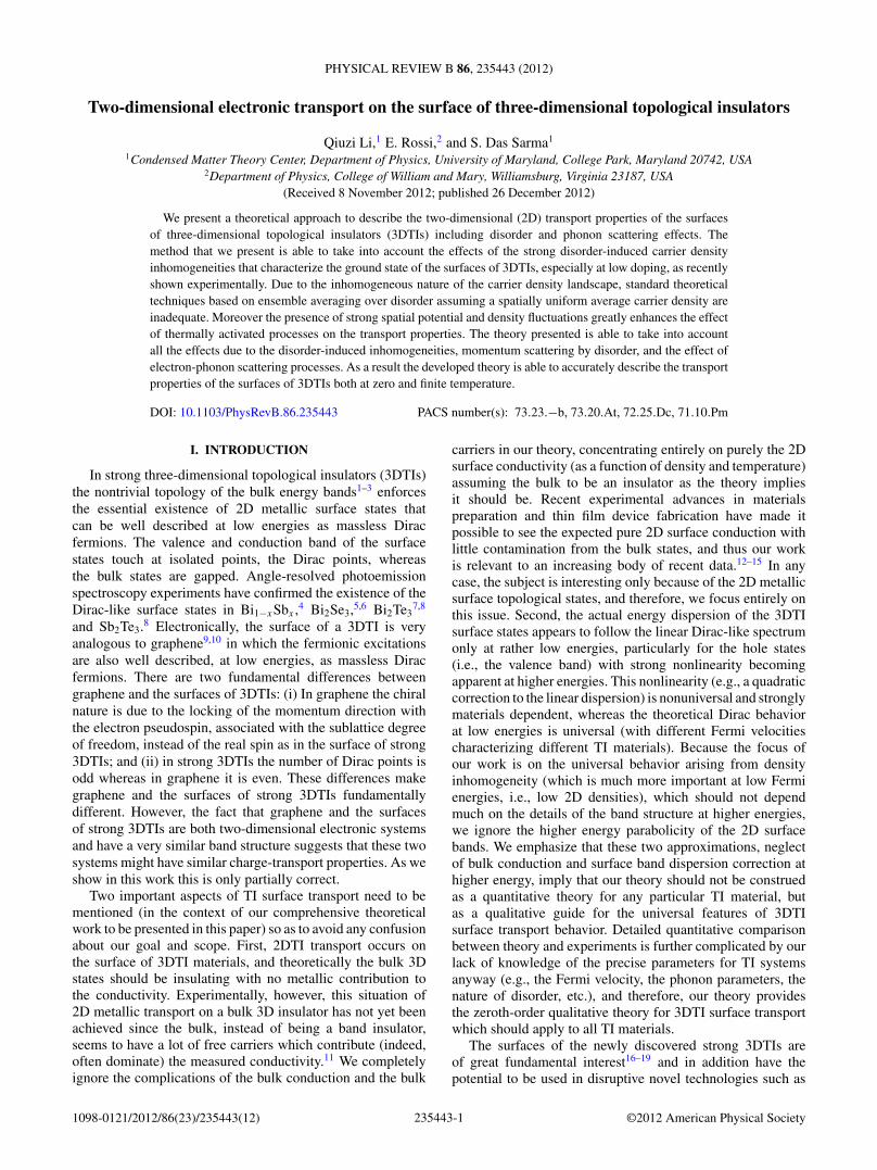
In Fig. 1, we show the carrier density profile calculatedusing the TFDT for a single disorder realization with chargedimpurity density nimp = 7.5 % 1013 cm!2 and two differentvalues for the impurity distances, d = 0.1 nm and d = 0.2 nmin panels (a) and (b) respectively. Unless otherwise specified,we use the background dielectric constant * = 50 for Bi2Se3and the Fermi velocity vF = 6.4 % 105 m/s.12,61
FIG. 1. (Color online) Color plots of carrier density distributionn(r) at the Dirac point for nimp = 7.5 % 1013 cm!2 and * = 50. Thecolor scale is in units of 1013 cm!2. (a) The impurity distance d =0.1 nm. (b) The impurity distance d = 0.2 nm.
235443-5
QIUZI LI, E. ROSSI, AND S. DAS SARMA PHYSICAL REVIEW B 86, 235443 (2012)
!5 0 50
0.2
0.4
0.6
0.8
1
n (1012 cm!2)
P(n
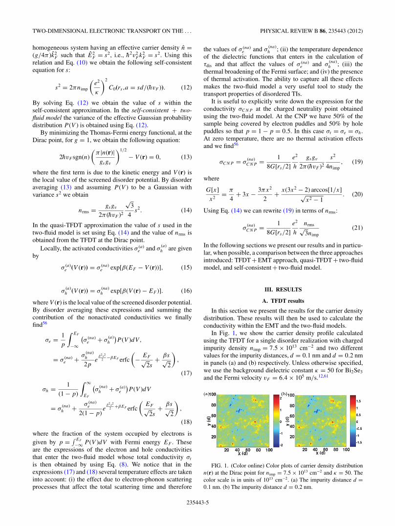
)DataFit!1Fit!2Fit!3
FIG. 2. (Color online) Density probability distribution at theDirac point for nimp = 7.5 % 1013 cm!2, d = 0.2 nm, and * = 50.The black line shows the TFDT result. The blue line is the fitP = be!|n/a| with a = 0.7 % 1012 cm!2 and b = 0.5309. The redline is the Gaussian fit to the tails of P (n), P = be!x2/a2
witha = 2.5 % 1012 cm!2 and b = .125. The green line is the Gaussian fitto the center of P (n), P = be!x2/a2
with a = 0.25 % 1012 cm!2 andb = 1.0.
Figure 1 conveys the nature of the carrier density landscapeon the surface of disordered 3DTIs as also shown recentlyby direct imaging experiments.28 To be able to make a quan-titative comparison with the experiments, and calculate theconductivity for large samples, using the TFDT we calculatethe disordered averaged density probability distribution P (n)for different parameter values such as doping, d and * . Asin graphene29 we find that P (n) obtained using the TFDTis bimodal, especially for finite values of the average carrierdensity, and so it is not well fitted by any single curve. Toexemplify this finding Fig. 2 shows P (n) at the CNP obtainedusing the TFDT and possible fitting curves. It is obvious fromthe figure that a reasonable fit can be obtained only by usingtwo different Gaussian curves, one to fit the very high peakcentered at n = 0 and one to fit the long tails of the distribution.
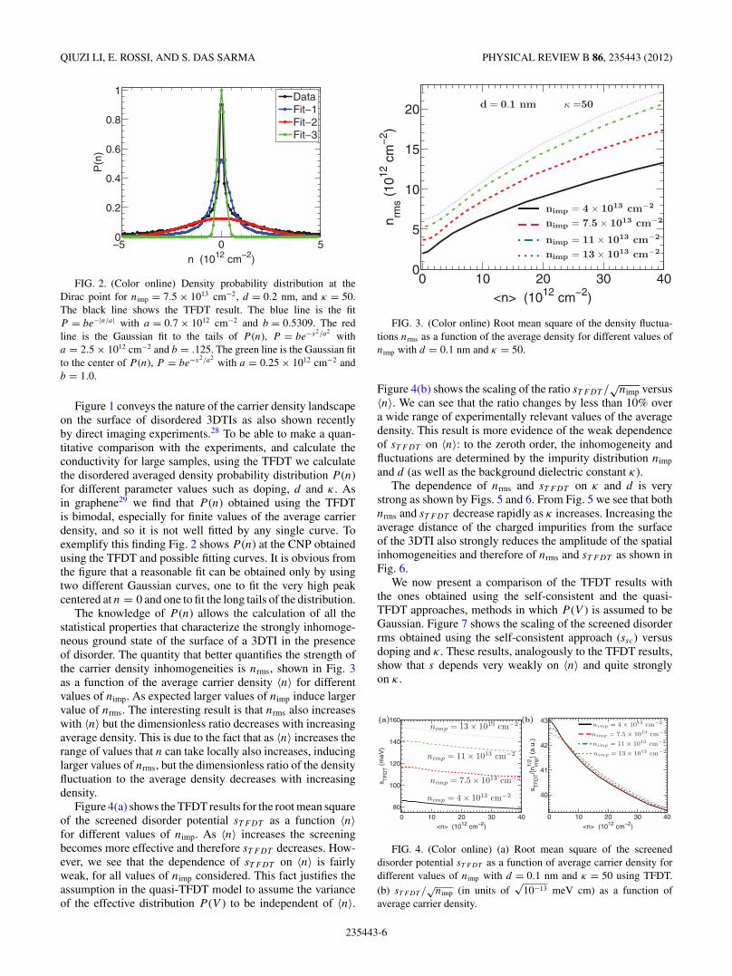
The knowledge of P (n) allows the calculation of all thestatistical properties that characterize the strongly inhomoge-neous ground state of the surface of a 3DTI in the presenceof disorder. The quantity that better quantifies the strength ofthe carrier density inhomogeneities is nrms, shown in Fig. 3as a function of the average carrier density #n$ for differentvalues of nimp. As expected larger values of nimp induce largervalue of nrms. The interesting result is that nrms also increaseswith #n$ but the dimensionless ratio decreases with increasingaverage density. This is due to the fact that as #n$ increases therange of values that n can take locally also increases, inducinglarger values of nrms, but the dimensionless ratio of the densityfluctuation to the average density decreases with increasingdensity.
Figure 4(a) shows the TFDT results for the root mean squareof the screened disorder potential sT FDT as a function #n$for different values of nimp. As #n$ increases the screeningbecomes more effective and therefore sT FDT decreases. How-ever, we see that the dependence of sT FDT on #n$ is fairlyweak, for all values of nimp considered. This fact justifies theassumption in the quasi-TFDT model to assume the varianceof the effective distribution P (V ) to be independent of #n$.
0 10 20 30 400
5
10
15
20
<n> (1012 cm!2)
n rms (
1012
cm
!2)
d = 0.1 nm ! =50
nimp = 4! 1013 cm!2
nimp = 7.5! 1013 cm!2
nimp = 11! 1013 cm!2
nimp = 13! 1013 cm!2
FIG. 3. (Color online) Root mean square of the density fluctua-tions nrms as a function of the average density for different values ofnimp with d = 0.1 nm and * = 50.
Figure 4(b) shows the scaling of the ratio sT FDT /,
nimp versus#n$. We can see that the ratio changes by less than 10% overa wide range of experimentally relevant values of the averagedensity. This result is more evidence of the weak dependenceof sT FDT on #n$: to the zeroth order, the inhomogeneity andfluctuations are determined by the impurity distribution nimpand d (as well as the background dielectric constant *).
The dependence of nrms and sT FDT on * and d is verystrong as shown by Figs. 5 and 6. From Fig. 5 we see that bothnrms and sT FDT decrease rapidly as * increases. Increasing theaverage distance of the charged impurities from the surfaceof the 3DTI also strongly reduces the amplitude of the spatialinhomogeneities and therefore of nrms and sT FDT as shown inFig. 6.
We now present a comparison of the TFDT results withthe ones obtained using the self-consistent and the quasi-TFDT approaches, methods in which P (V ) is assumed to beGaussian. Figure 7 shows the scaling of the screened disorderrms obtained using the self-consistent approach (ssc) versusdoping and * . These results, analogously to the TFDT results,show that s depends very weakly on #n$ and quite stronglyon * .
0 10 20 30 4080
100
120
140
160
<n> (1012 cm!2)
s TF
DT (
meV
)
0 10 20 30 40
40
41
42
43
<n> (1012 cm!2)
s TF
DT/[n
1/2
imp] (
a.u.
)
= 4 ! 1013 cm!2
= 7.5 ! 1013 cm!2
= 11 ! 1013 cm!2
= 13 ! 1013 cm!2)b()a(
= 4 " 10 cm
= 7.5 " 10 cm
= 11 " 10 cm
= 13 " 10 cm
FIG. 4. (Color online) (a) Root mean square of the screeneddisorder potential sT FDT as a function of average carrier density fordifferent values of nimp with d = 0.1 nm and * = 50 using TFDT.(b) sT FDT /
,nimp (in units of
,10!13 meV cm) as a function of
average carrier density.
235443-6

TWO-DIMENSIONAL ELECTRONIC TRANSPORT ON THE . . . PHYSICAL REVIEW B 86, 235443 (2012)
0 20 40 60 80 100
10
10
10
!
n rms (
1012
cm
!2)
0 20 40 60 80 100
10
10
!
s TF
DT (
meV
)
= 4 ! 1013 cm!2
= 11 ! 1013 cm!2
)b()a(
= 4 ! 1013 cm!2
= 11 ! 1013 cm!2
FIG. 5. (Color online) TFDT results at the CNP for d = 0.1 nm.(a) nrms as a function of substrate dielectric constant * . (b) Rootmean square of the screened disorder potential sT FDT as a functionof substrate dielectric constant * . The solid lines are for nimp = 4 %1013 cm!2 and the dashed lines are for nimp = 11.0 % 1013 cm!2.
Figure 8 shows the comparison for the value of s at the CNPas a function of d obtained using the three different methods:TFDT, quasi-TFDT, and self-consistent. We see that the self-consistent approach in general returns values of s larger thanthe ones obtained using the TFDT. We should emphasize thats obtained using the quasi-TFDT method is only an effectivequantity that is used to calculate the transport properties withinthe two-fluid model.
B. Transport at zero temperature
Using the TFDT and the EMT we can calculate the 2Dconductivity on the surface of a 3DTI. Figure 9 shows ! as afunction of doping, i.e., average density, for several values ofnimp and fixed d = 0.1 nm and * = 50. As in graphene10 theTFDT + EMT results recover the behavior of ! (n) observedexperimentally:12 the linear scaling of ! (n) at large doping,the finite value (!min) of ! for n = 0, and the crossoverregime for intermediate values of n. More importantly, thetheory returns values of !min = (2 ! 4)e2/h (depending on
0 1 2 3
10
10
d (nm)
n rms (
1012
cm
!2)
0 1 2 3
10
10
d (nm)
n rms (
1012
cm
!2)
0 1 2 3
100
200
400
d (nm)
s TF
DT (
meV
)
0 1 2 3
40
80
d (nm)
s TF
DT (
meV
)
)b()a( = 5 = 50= 4 ! 1013 cm!2 = 4 ! 1013 cm!2
= 0 meV
= 40 meV
= 100 meV
= 0 meV
= 40 meV
= 100 meV
)d()c( = 5 = 50= 4 ! 1013 cm!2 = 4 ! 1013 cm!2
= 0 meV
= 40 meV
= 100 meV= 0
= 40 meV
= 100 meV
FIG. 6. (Color online) (a) and (b) nrms at the Dirac point versus thedistance d of the charged impurity to the TI surface calculated withinTFDT for nimp = 4.0 % 1013 cm!2. The solid, dashed, and dot-dashedlines correspond to chemical potential EF = 0, 40, and 100 meV,respectively. (c), (d) The corresponding sT FDT results versus d . (a),(c) The effective background dielectric constant * = 5. (b), (d) Theeffective background dielectric constant * = 50.
0 10 20 30 4034
36
38
40
42
44
46
n (1012 cm!2)
s sc/[n
1/2
imp] (
a.u.
)
0 20 40 60 80 100
10
10
!
s sc (
meV
)
(a) (b)
nimp = 4! 1013 cm"2
nimp = 7.5! 1013 cm"2
nimp = 11 ! 1013 cm"2
nimp = 13 ! 1013 cm"2
= 50
nimp = 11 ! 1013 cm"2
nimp = 4! 1013 cm"2
FIG. 7. (Color online) Self-consistent results. (a) ssc/,
nimp (inunits of
,10!13 meV cm) as a function of carrier density for different
values of nimp with * = 50 and d = 0.1 nm. (b) Potential fluctuationssc as a function of substrate dielectric constant * . The solid linesare for nimp = 4 % 1013 cm!2 and the dashed lines are for nimp =11.0 % 1013 cm!2 with d = 0.1 nm.
the sample properties) that agree with the ones observed inexperiments.12
Figure 10 shows the comparison for the dependence of !with respect to n obtained using the TFDT + EMT methodand the two-fluid approximations. From Fig. 10 we see thatfor nimp " 4 % 1013 cm!2 and values of * ! 50, the threeapproaches give very similar results. For smaller values of *the three approaches give results that are qualitatively similarbut that differ quantitatively. The general conclusion is thataway from the CNP the three approaches agree quantitativelyfor samples with mobility µ > 1000 cm2/V s. For very lowmobility highly disordered TI systems (with 2D surfacemobility lower than 1000 cm2/V s even at T = 0), we expectthe TFDT to provide the most quantitatively accurate results.However, given that our main objective is to describe theuniversal qualities of the transport arising from the presence ofinhomogeneities, and given the absence of accurate knowledgeof the impurity distribution, i.e., nimp and d in our model, forthe purposes of this work the three approaches appear to beequivalent.
Close to the CNP the three transport approaches giveresults that differ quantitatively, as shown in Figs. 11–13.The self-consistent + two-fluid model for the parameter valuesrelevant for TIs gives values of !min smaller than the onesobtained using the TFDT + EMT method. In TIs the agreementbetween the two methods close to the CNP is worse than ingraphene62 due to the fact that in TIs the density of charged
0 1 2 3
10
10
d (nm)
s (m
eV)
0 1 2 3
10
d (nm)
s (m
eV)
)b()a(
= 5 = 50= 4 ! 1013 cm!2 = 4 ! 1013 cm!2
TFDT
quasi-TFDT
self-consistent
TFDT
quasi-TFDT
self-consistent
FIG. 8. (Color online) Comparison of three methods for thepotential fluctuation s at the Dirac point versus the charged impuritydistance d to the TI surface for nimp = 4.0 % 1013 cm!2. The solid,dashed, and dot-dashed lines correspond to the TFDT, quasi-TFDT,and the self-consistent methods, respectively. (a) The effectivebackground dielectric constant * = 5. (b) The effective backgrounddielectric constant * = 50.
235443-7

QIUZI LI, E. ROSSI, AND S. DAS SARMA PHYSICAL REVIEW B 86, 235443 (2012)
0 2 4 6 8 100
10
20
30
40
<n> (1012 cm!2)
" (e
2 /h)
nimp = 4! 1013 cm!2
nimp = 7.5! 1013 cm!2
nimp = 11! 1013 cm!2
nimp = 13! 1013 cm!2
FIG. 9. (Color online) TFDT-EMT conductivity as a function ofaverage carrier density for different values of nimp with d = 0.1 nmand * = 50.
impurities is larger than in typical graphene samples. It isremarkable to see how, in agreement with experiments, thethree methods give the result that !min depends very weaklyon nimp and * , for experimentally relevant parameter values.The weak dependence on nimp can be qualitatively understoodusing the two-fluid model result for !min Eq. (19) from whichwe see that !min is proportional to the ratio s2/nimp, and thaton the other hand s2 is proportional to nimp, Eq. (12). Withinthe semiclassical approach the very weak dependence of!min on nimp and * is due to the fact that an increase(decrease) of nimp (*) increases the strength of the disorderpotential that causes a decrease of the carriers mean freepath ., and an increase of the amplitude of the carrierdensity inhomogeneities (i.e., the density of carriers in theelectron-hole puddles). The reduction of . and the increaseof nrms have opposite effects on !min and they almost cancelout.40,63
The dependence of !min with respect to the average distanced of the charged impurities from the TIs surface is appreciablydifferent for the three methods. The self-consistent + two-fluidmodel returns a very weak dependence of !min with respect tod. This is due to the weak dependence with respect to d ofs2 obtained using the self-consistent approximation, Eq. (12).On the other hand the value of s2 obtained using the TFDT isquite sensitive to the value of d and as a consequence usingthe TFDT + EMT and the quasi-TFDT + two-fluid models we
0 10 20 30 40 500
5
10
15
20
25
<n> (1012 cm!2)
" (e
2 /h)
!=10!=20
0 2 4 6 8 100
50
100
150
<n> (1012 cm!2)
" (e
2 /h)
!=50!=80!=100
)b()a(
FIG. 10. (Color online) Calculated conductivity as a functionof carrier density for different values of the substrate dielectricconstant with the impurity density nimp = 4.0 % 1013 cm!2, d =0.1 nm. The solid, dashed, and dot-dashed lines are obtained by usingthe TFDT-EMT method, self-consistent method, and quasi-TFDTmethod, respectively.
4 6 8 10 12 140
1
2
3
4
5
6
nimp
(1013 cm!2)
" min
(e2 /h
)
= 1 A
= 2 A
= 1 A= 2 A
= 1 A
= 2 A
TFDT
quasi-TFDT
self-consistent
FIG. 11. (Color online) The minimum conductivity !min as afunction of charged impurity density nimp with * = 50. The symbolsdiamond, circle, and square denote the results obtained using thequasi-TFDT, TFDT-EMT, and the self-consistent method, respec-tively. The solid and dashed lines correspond to the impurity distancesd = 1 A and d = 2 A, respectively.
find that the dependence of !min on d is not as weak as the onegiven from the self-consistent + two-fluid model. All the threeapproaches show that !min decreases as a function of d. Thisis due to the fact that as d increases, due to the weakening ofthe disorder potential, the decrease of nrms is faster than theincrease of the mean free path.
C. Transport at finite temperature
In this section, using the two-fluid model, we present ourresults for the conductivity in TIs at finite temperature. Ifwe neglect the contribution of activation processes in TIs,the dominant contribution to the temperature dependence of! is due to electron-phonon scattering processes. Figure 14shows the longitudinal acoustic phonon limited resistivity ofthe Bi2Se3 surface as a function of temperature on a log-logplot. To calculate the Bi2Se3 surface resistivity due to phononscattering37 we use D = 30 eV for the deformation potentialcoupling constant, ,m . 7.68 % 10!7 g/cm!2 for the twodimensional mass density, i.e., 1 quintuple layer mass densityof Bi2Se3, and vl = 2900 m/s is the velocity of the longitudinal
0 20 40 60 80 1000
1
2
3
4
5
!
" min
(e2 /h
)
= 4 ! 1013 cm!2
TFDT
quasi-TFDT
self-consistent
FIG. 12. (Color online) The minimum conductivity !min asa function background dielectric constant * for nimp = 4.0 %1013 cm!2, d = 0.1 nm. The dashed, solid, and dot-dashed linesdenote the results obtained using the quasi-TFDT, TFDT-EMT, andthe self-consistent method, respectively.
235443-8

TWO-DIMENSIONAL ELECTRONIC TRANSPORT ON THE . . . PHYSICAL REVIEW B 86, 235443 (2012)
0 1 2 30
1
2
3
4
5
d (nm)
" min
(e2 /h
)
0 1 2 30
1
2
3
4
5
d (nm)
" min
(e2 /h
)
= 5 = 50= 4 ! 1013 cm!2 = 4 ! 1013 cm!2
)b()a(
TFDTquasi-TFDTself-consistent
TFDTquasi-TFDTself-consistent
FIG. 13. (Color online) The minimum conductivity !min versusthe charged impurity distance d to the TI surface for nimp =4.0 % 1013 cm!2. The solid, dashed, and dot-dashed lines correspondto the TFDT-EMT, quasi-TFDT, and the self-consistent methods,respectively. (a) The effective background dielectric constant * = 5.(b) The effective background dielectric constant * = 50.
acoustic phonon mode.37 The inset of Fig. 14 shows thelogarithmic derivatives of the temperature-dependent resis-tivity. Fig. 14 clearly demonstrates two different regimesdepending on whether the phonon system is degenerate ornondegenerate, and the low- to high-temperature crossoveris characterized by the Bloch-Gruneisen (BG) temperatureTBG = 2kF vl/kB .35–37,64 The resistivity increases with T as, ) T 4 at low temperatures and , ) T at high temperatures,which agrees with the results obtained for TI films by using anisotropic elastic continuum approach.37 We note that electron-phonon scattering is an important scattering mechanism forfinite-temperature transport in TIs, e.g., TBG ) 30 K in TIscompared to TBG ) 100 K in graphene because the latter hasmuch larger phonon velocity. In graphene, in contrast to 2Dsurface TI transport, phonon effects are extremely weak.35
The results shown in Fig. 14 do not include the contributionto the resistivity due to quenched disorder. To include both theeffect of quenched disorder and electron-phonon scatteringwe use the quasi-TFDT + two-fluid model. As discussedin Sec. II, this approach allows us to take into accountseveral finite temperature effects: the temperature dependence
0.1 1 10 100T (K)
10-4
10-2
100
102
104
# ($
)
n=1010
cm-2
n=1011
cm-2
n=1012
cm-2
n=1013
cm-2
1 10 100T (K)
0
1
2
3
4
5
dlog
#/dl
ogT
# T 4
# T
FIG. 14. (Color online) Double-logarithmic scale of resistivity(Bi2Se3) only due to phonon scattering as a function of temperaturefor several densities. The deformation potential coupling constantD = 30 eV, ,m . 7.68 % 10!7 g/cm!2, and the velocity of longi-tudinal acoustic phonon mode vl = 2900 m/s. The inset shows thelogarithmic derivatives d log ,/d log T versus temperature.
0 100 200 3001
1.05
1.1
1.15
1.2
T (K)
" (T
)/" (
T=5
K)
0 100 200 3001
1.1
1.2
1.3
1.4
1.5
1.6
T (K)
" (T
)/" (
T=5
K)
)b()a( d = 0.1 nm n = 2.27! 10 cm d = 1 nm n = 1.0! 10 cm
gnirettacsytirupmidegrahcylnognirettacsytirupmidegrahcylno
n = 10 cmn = 10 cm
n = 2! 10 cmn = 3! 10 cm
n = 10 cmn = 10 cm
n = 2! 10 cmn = 3! 10 cm
FIG. 15. (Color online) Calculated conductivity as a functionof temperature for different carrier density including only chargedimpurity scattering with d = 0.1 nm, * = 50, and nimp = 4 %1013 cm!2. (a) The charged impurity distance d = 0.1 nm. Thecorresponding TFDT nrms . 2.27 % 1012 cm!2 and the potentialfluctuation s . 220 meV [Eq. (14)]. (b) The charged impuritydistance d = 1 nm. The corresponding TFDT nrms . 1.0 % 1012
cm!2 and the potential fluctuation s . 150 meV [Eq. (14)].
of the screening of the quenched disorder, electron-phononscattering processes, broadening of the Fermi surface, andtemperature-induced activated processes. The temperatureactivated processes cause ! to increase with T and thereforeinduce an insulating behavior (i.e., conductivity increasingwith increasing temperature) for ! (T ), whereas the electron-phonon scattering processes induce a metallic behavior (i.e.,conductivity decreasing with increasing temperature). Thechange with T of the screening of the disorder potential alsoinduces a metallic behavior for ! (T ); however, given the largevalue of * in typical TIs this effect is quite weak, contraryto the case of graphene10 or 2D semiconductor systems.65
Figures 15(a) and 15(b) show the dependence of ! on Tobtained by neglecting the effect of electron-phonon scatteringprocesses. We see that in this case the temperature dependenceof ! is almost completely determined by thermally activatedprocesses that induce a monotonic increase of ! with T .
Figure 16 shows the scaling of the conductivity withrespect to doping at different temperatures including both theeffects of quenched disorder and electron-phonon scattering.At large densities the main effect of the finite temperatureis to suppress ! due to the presence of electron-phononscattering processes. However, at low densities the effect ofelectron-phonon scattering processes competes with thermalactivation processes and can give rise to a nonmonotonic
0 2 4 6 8 100
10
20
30
40
<n> (1012 cm!2)
" (e
2 /h)
0 5 10 150
5
10
15
20
25
<n> (1012 cm!2)
" (e
2 /h)
)b()a(
T = 0 KT = 20 K
T = 40 KT = 60 K
T = 0 KT = 20 K
T = 40 KT = 60 K
n = 4! 10 cm n = 11! 10 cm
FIG. 16. (Color online) Calculated conductivity as a functionof net carrier density for various temperatures with d = 0.1 nmand * = 50. (a) The impurity density nimp = 4 % 1013 cm!2. Thecorresponding TFDT nrms . 2.27 % 1012 cm!2 and the potentialfluctuation s . 220 meV [Eq. (14)]; (b) The impurity density nimp =11 % 1013 cm!2. The corresponding TFDT nrms . 4.21 % 1012 cm!2,and the potential fluctuation s . 300 meV [Eq. (14)].
235443-9

QIUZI LI, E. ROSSI, AND S. DAS SARMA PHYSICAL REVIEW B 86, 235443 (2012)
0 100 200 3000.5
0.6
0.7
0.8
0.9
1
1.1
T (K)
" (T
)/" (
T=5
K)
0 100 200 3000.2
0.4
0.6
0.8
1
1.2
T (K)
" (T
)/" (
T=5
K)
n = 10 cmn = 10 cm
n = 2! 10 cmn = 3! 10 cm
d = 0.1 nm n = 2.27! 10 cm d = 1 nm n = 1.0! 10 cm)b()a(
n = 10 cm
n = 10 cm
n = 2! 10 cm
n = 3! 10 cm
FIG. 17. (Color online) Calculated conductivity as a function oftemperature for different carrier densities including both chargedimpurity and electron-phonon scattering, with d = 0.1 nm, * =50, and nimp = 4 % 1013 cm!2. (a) The charged impurity distanced = 0.1 nm. The corresponding TFDT nrms . 2.27 % 1012 cm!2,and the potential fluctuation s . 220 meV [Eq. (14)]. (b) Thecharged impurity distance d = 1 nm. The corresponding TFDTnrms . 1.0 % 1012 cm!2 and the potential fluctuation s . 150 meV[Eq. (14)].
dependence of ! with respect to T . This is shown in Figs. 17(a)and 17(b) where ! (T ) for different values of n is plotted.From Figs. 17(a) and 17(b) we see that for n " nrms atlow temperatures the thermal activation processes dominateand induce an insulating behavior for ! (T ). The crossovertemperature from insulating to metallic behavior depends onn, nimp, * and d. In general the larger the strength of thespatial fluctuations of the carrier density the stronger is theeffect of thermal activation processes and therefore the largeris the low temperature range for which the transport exhibitsinsulating behavior. This is shown clearly by the scaling of! (T ) at the CNP for different values of nimp, * , Figs. 18(a)and 18(b), respectively. From Figs. 18(a) and 18(b) we seethat a change of nimp and * that increases nrms extends the
0 100 200 3000.96
0.98
1
1.02
1.04
T (K)
" min
(T
)/"m
in (
T=5
K)
0 100 200 300
0.95
1
1.05
1.1
T (K)
" min
(T
)/"m
in (
T=5
K)
0 100 200 300
1
1.1
1.2
1.3
1.4
1.5
1.6
T (K)
" min
(T
)/"m
in (
T=5
K)
(b)(a)
(c)
n = 4! 10 cmn = 7.5! 10 cm
n = 11! 10 cmn = 13! 10 cm
= 10= 20
= 50= 100
d = 0.1 nmd = 0.5 nm
d = 1 nmd = 1.5 nm
= 50 d = 0.1 nm
n = 4! 10 cm d = 0.1 nm
n = 4! 10 cm = 50
FIG. 18. (Color online) Minimum conductivity as a function oftemperature (a) for various charged impurity densities nimp. As nimp
increases, the corresponding s = 220, 300, 360, and 390 meV; (b)for various dielectric constants * . As * increases, the correspondings = 840, 500, 220, and 110 meV; (c) for various charged impuritydistances d . As d increases, the corresponding s = 220, 180, 150, and130 meV. The corresponding potential fluctuation s is obtained viaEq. (14) using nrms calculated within the TFDT (shown in Figs. 3, 5,and 6).
range of temperatures over which !min(T ) exhibit an insulatingbehavior.
The temperature dependence of ! for different values of dis shown in Fig. 18(c). It appears to contradict the general rulethat a parameter change that increases nrms will increase therange of temperatures over which ! (T ) exhibit an insulatingbehavior. This is due to the combination of two effects: (i)The fact that at large d (d ! 1 nm) nrms is very low andso the resistivity ,dis due to the quenched disorder at lowcarrier densities is much higher than the resistivity ,ph dueto electron-phonon scattering, so that !tot(T )/!tot(T = 5K) &!dis(T )/!dis(T = 5K); and (ii) the decrease at large d of themetallic screening effects. The scaling of ! with respect toT and d is therefore very interesting because it reveals thetemperature dependence of the screening and could thereforebe used to indirectly identify the nature of the disorder potentialand the screening properties of the surfaces of 3DTIs.
Before concluding this section on the temperature-dependent surface conductivity of 3DTIs, we point out thatone of the important qualitative findings of our work is thenonmonotonic temperature dependence of the 2D surfaceconductivity as apparent in Figs. 16–18 and as expected fromthe competing mechanisms of phonon scattering and disor-der induced density inhomogeneity. In particular, phononsinduce higher-temperature metallic temperature dependenceand the density inhomogeneity induces insulating temperaturedependence through thermal activation, and at some disorder-dependent (and also doping-dependent) characteristic temper-ature the transport behavior changes from being insulating-like to metallic-like. We emphasize that this temperature-induced crossover behavior has nothing to do with anylocalization phenomenon (and in fact, Anderson localizationeffects are completely absent in TI surface transport sinceall back scattering is suppressed), and it arises entirely froma competition between inhomogeneity and phonons. Themetallic behavior moves to higher (lower) temperature asdisorder increases (decreases). This nonmonotonicity has beenobserved in experiments at lower 2D carrier densities34 wherethe inhomogeneity effects are important.
IV. CONCLUSIONS
We have presented a detailed theoretical study of the2D transport properties of the surfaces of 3DTIs. There iscompelling evidence that in current transport experiments on3DTIs charged impurities are the dominant source of quencheddisorder. For this reason in our study we have considered indetail the case in which the quenched disorder potential isthe one created by random charged impurities close to thesurface of the TI. However, the theoretical framework that wehave developed and presented in this work is very general.As in graphene, the presence of charged impurities inducesthe formation of strong carrier density inhomogeneities. Inparticular, close to the charge neutrality point the carrierdensity landscape breaks up in electron-hole puddles. Thestrong carrier density inhomogeneities make the theoreticaldescription of the electronic transport challenging for tworeasons: (i) inability to use standard theoretical methods thatassume a homogeneous density landscape; and (ii) the impor-tance at finite temperature of thermally activated processes.
235443-10

TWO-DIMENSIONAL ELECTRONIC TRANSPORT ON THE . . . PHYSICAL REVIEW B 86, 235443 (2012)
Our work presents a theoretical description of transport onthe surface of 3DTIs that overcomes these difficulties andtakes into account also the effect of electron-phonon scatteringprocesses which is an important resistive mechanism at highertemperatures.
To characterize the disorder-induced inhomogeneities weuse the Thomas-Fermi-Dirac theory. We also present acomparison of the results obtained using the TFDT with theone obtained using the self-consistent approximation and thequasi-TFDT approach and show that the three approachesgive results that are qualitatively similar but that differquantitatively.
To study the electronic transport in the presence of strongcarrier density inhomogeneities, starting from the TFDTresults, we use the effective medium theory and a two-fluidmodel. The TFDT + EMT approach is well justified andis expected to provide the most accurate results. However,the generalization of the TFDT + EMT method to finitetemperature is impractical due to the contribution to transportof thermally activated processes, contribution that can bedominant at low temperatures due to the strong carrier densityinhomogeneities. At finite temperature the two-fluid approachis very valuable because it allows us to take into account allthe finite temperature effects, such as temperature-dependentscreening and electron-phonon scattering, including thermallyactivated processes. The two-fluid model relies on the use of aneffective Gaussian distribution for the probability distributionof the screened potential P (V ). The parameters that defineP (V ) can be chosen in such a way to maximize the agreementof the results for T = 0 obtained using the two-fluid model andthe ones obtained using the TFDT + EMT approach. Theseparameters are then used to obtain the transport properties atfinite temperature using the two-fluid model.
In current 3DTIs the dielectric constant (* ) 50) is muchlarger than in graphene where * ) 1–4. In addition, in 3DTIsthe acoustic phonon velocity is smaller than in graphene. Thesefacts make the contribution of electron-phonon scatteringprocesses to the resistivity much more important in the surfaceof 3DTIs than in graphene. For the surfaces of 3DTIs theeffect of electron-phonon scattering events becomes importantalready for T as low as 10 K, whereas in graphene it becomes
relevant only for T ! 200 K. As a consequence for the surfacesof 3DTIs we find that electron-phonon scattering is much moreimportant to determine the dependence of the conductivityon T . The large value of * in 3DTIs also implies that forthe surface of 3DTIs, contrary to graphene, the temperaturedependence of the screening does not play an important role.The temperature dependence of the conductivity on the surfaceof 3DTIs is therefore mostly determined by electron-phononscattering processes and thermal activations processes. Thesetwo types of processes have opposite effects on ! , and atlow temperature and low doping they compete, giving riseto a nonmonotonic dependence of ! with respect to T . Thenonmonotonic temperature dependence of the 2D surfaceconductivity is one of the important new qualitative resultsof our theory. We have presented detailed results for ! (T ) thatclearly show the competition of the different processes thataffect ! for T /= 0.
The theoretical approach developed here, being able toinclude all the main effects that determine the transportproperties of the surfaces of 3DTIs, allowed us to presentresults that can be directly and quantitatively compared to theexperimental ones. The good agreement between our theoret-ical results and the recent experimental measurements,12–15,34
suggest that the theoretical method presented is very effectiveto characterize the transport properties of the surfaces of3DTIs, especially due to its ability to take into account theeffects due to the disorder-induced carrier density inhomo-geneities. Future improvement of the theory could include amore accurate surface band structure and the effects of thebulk bands, but we do not expect these details to affect ourqualitative results at low surface doping densities becauseour theory includes the most important resistive processescontributing to the surface transport in 3DTIs.
ACKNOWLEDGMENTS
Q. L. acknowledges helpful discussions with EuyheonHwang. This work is supported by ONR-MURI, LPS-CMTC,and NRI-SWAN. E.R. acknowledges support from the JeffressMemorial Trust, Grant No. J-1033, and the faculty researchgrant program from the College of William and Mary.
1M. Z. Hasan and C. L. Kane, Rev. Mod. Phys. 82, 3045 (2010).2L. Fu, C. L. Kane, and E. J. Mele, Phys. Rev. Lett. 98, 106803(2007).
3D. Culcer, Physica E 44, 860 (2012).4D. Hsieh, D. Qian, L. Wray, Y. Xia, Y. S. Hor, R. J. Cava, andM. Z. Hasan, Nature (London) 452, 970 (2008).
5Y. Xia, D. Qian, D. Hsieh, L. Wray, A. Pal, H. Lin, A. Bansil,D. Grauer, Y. S. Hor, R. J. Cava, and M. Z. Hasan, Nat. Phys. 5,398 (2009).
6Y. Hsieh, D. Xia, D. Qian, L. Wray, J. H. Dil, F. Meier, J.Osterwalder, L. Patthey, J. G. Checkelsky, N. P. Ong, A. V. Fedorov,H. Lin, A. Bansil, D. Grauer, Y. S. Hor, R. J. Cava, and M. Z. Hasan,Nature (London) 460, 1101 (2009).
7Y. Chen, J. Analytis, J. Chu, Z. Liu, S. Mo, X. Qi, H. Zhang, D. Lu,X. Dai, Z. Fang, S.-C. Zhang, I. R. Fisher, Z. Hussain, and Z.-X.Shen, Science 325, 178 (2009).
8D. Hsieh, Y. Xia, D. Qian, L. Wray, F. Meier, J. H. Dil, J.Osterwalder, L. Patthey, A. V. Fedorov, H. Lin, A. Bansil, D. Grauer,Y. S. Hor, R. J. Cava, and M. Z. Hasan, Phys. Rev. Lett. 103, 146401(2009).
9K. S. Novoselov, A. K. Geim, S. V. Morozov, D. Jiang, Y. Zhang,S. V. Dubonos, I. V. Grigorieva, and A. A. Firsov, Science 306, 666(2004).
10S. Das Sarma, S. Adam, E. H. Hwang, and E. Rossi, Rev. Mod.Phys. 83, 407 (2011).
11N. P. Butch, K. Kirshenbaum, P. Syers, A. B. Sushkov, G. S.Jenkins, H. D. Drew, and J. Paglione, Phys. Rev. B 81, 241301(2010).
12D. Kim, S. Cho, N. P. Butch, P. Syers, K. Kirshenbaum, J. Paglione,and M. S. Fuhrer, Nat. Phys. 8, 460 (2012).
13S. S. Hong, J. J. Cha, D. Kong, and Y. Cui, Nat. Commun. 3, 757(2012).
235443-11

QIUZI LI, E. ROSSI, AND S. DAS SARMA PHYSICAL REVIEW B 86, 235443 (2012)
14D. Kong, Y. Chen, J. J. Cha, Q. Zhang, J. G. Analytis, K. Lai,Z. Liu, S. S. Hong, K. J. Koski, S.-K. Mo, Z. Hussain, I. R. Fisher,Z.-X. Shen, and Y. Cui, Nat. Nanotechnol. 6, 705 (2011).
15H. Steinberg, J.-B. Laloe, V. Fatemi, J. S. Moodera, and P.Jarillo-Herrero, Phys. Rev. B 84, 233101 (2011).
16F. Wilczek, Phys. Rev. Lett. 58, 1799 (1987).17X.-L. Qi, T. L. Hughes, and S.-C. Zhang, Phys. Rev. B 78, 195424
(2008).18F. Wilczek, Nature (London) 458, 129 (2009).19R. Li, J. Wang, X.-L. Qi, and S.-C. Zhang, Nat. Phys. 6, 284 (2010).20L. Fu and C. L. Kane, Phys. Rev. Lett. 100, 096407 (2008).21L. Fu and C. L. Kane, Phys. Rev. B 79, 161408 (2009).22J. E. Moore, Nature (London) 464, 194 (2010).23M. Liu, C.-Z. Chang, Z. Zhang, Y. Zhang, W. Ruan, K. He, L.-l.
Wang, X. Chen, J.-F. Jia, S.-C. Zhang, Q.-K. Xue, X. Ma, andY. Wang, Phys. Rev. B 83, 165440 (2011).
24D. Culcer, E. H. Hwang, T. D. Stanescu, and S. Das Sarma, Phys.Rev. B 82, 155457 (2010).
25S. Adam, E. H. Hwang, and S. Das Sarma, Phys. Rev. B 85, 235413(2012).
26J. Martin, N. Akerman, G. Ulbricht, T. Lohmann, J. H. Smet, K. V.Klitzing, and A. Yacoby, Nat. Phys. 4, 144 (2008).
27Y. Zhang, V. W. Brar, C. Girit, A. Zettl, and M. F. Crommie, Nat.Phys. 5, 722 (2009); A. Deshpande, W. Bao, F. Miao, C. N. Lau,and B. J. LeRoy, Phys. Rev. B 79, 205411 (2009); A. Deshpande,W. Bao, Z. Zhao, C. N. Lau, and B. J. LeRoy, ibid. 83, 155409(2011).
28H. Beidenkopf, P. Roushan, J. Seo, L. Gorman, I. Drozdov, Y. S.Hor, R. J. Cava, and A. Yazdani, Nat. Phys. 7, 939 (2011).
29E. Rossi and S. Das Sarma, Phys. Rev. Lett. 101, 166803 (2008).30R. C. Hatch, M. Bianchi, D. Guan, S. Bao, J. Mi, B. B. Iversen,
L. Nilsson, L. Hornekær, and P. Hofmann, Phys. Rev. B 83, 241303(2011).
31E. H. Hwang and S. Das Sarma, Phys. Rev. B 75, 205418 (2007).32N. Kumar, B. A. Ruzicka, N. P. Butch, P. Syers, K. Kirshenbaum,
J. Paglione, and H. Zhao, Phys. Rev. B 83, 235306 (2011).33W. Richter and C. R. Becker, Phys. Status Solidi B 84, 619 (1977).34D. Kim, Q. Li, P. Syers, N. P. Butch, J. Paglione, S. D. Sarma, and
M. S. Fuhrer, Phys. Rev. Lett. 109, 166801 (2012).35E. H. Hwang and S. Das Sarma, Phys. Rev. B 77, 115449 (2008).36S. Giraud and R. Egger, Phys. Rev. B 83, 245322 (2011).37S. Giraud, A. Kundu, and R. Egger, Phys. Rev. B 85, 035441 (2012).38C.-X. Liu, X.-L. Qi, H. J. Zhang, X. Dai, Z. Fang, and S.-C. Zhang,
Phys. Rev. B 82, 045122 (2010).
39M. Polini, A. Tomadin, R. Asgari, and A. H. MacDonald, Phys.Rev. B 78, 115426 (2008).
40E. Rossi, S. Adam, and S. Das Sarma, Phys. Rev. B 79, 245423(2009).
41L. Brey and H. A. Fertig, Phys. Rev. B 80, 035406 (2009).42S. Das Sarma and E. H. Hwang, Phys. Rev. Lett. 102, 206412
(2009).43E. Rossi and S. Das Sarma, Phys. Rev. Lett. 107, 155502 (2011).44M. M. Fogler, D. S. Novikov, L. I. Glazman, and B. I. Shklovskii,
Phys. Rev. B 77, 075420 (2008).45C. Beenakker, Rev. Mod. Phys. 80, 1337 (2008).46M. I. Katsnelson, K. S. Novoselov, and A. K. Geim, Nat. Phys. 2,
620 (2006).47A. V. Shytov, M. S. Rudner, and L. S. Levitov, Phys. Rev. Lett. 101,
156804 (2008).48N. Stander, B. Huard, and D. Goldhaber-Gordon, Phys. Rev. Lett.
102, 026807 (2009).49A. Young and P. Kim, Nat. Phys. 5, 222 (2009).50E. Rossi, J. H. Bardarson, P. W. Brouwer, and S. Das Sarma, Phys.
Rev. B 81, 121408R (2010).51D. A. G. Bruggeman, Ann. Phys. (N.Y.) 416, 636 (1935).52R. Landauer, J. Appl. Phys. 23, 779 (1952).53M. Hori and F. Yonezawa, J. Math. Phys. 16, 352 (1975).54M. M. Fogler, Phys. Rev. Lett. 103, 236801 (2009).55E. Rossi, J. H. Bardarson, M. S. Fuhrer, and S. Das Sarma, Phys.
Rev. Lett. 109, 096801 (2012).56Q. Li, E. H. Hwang, and S. Das Sarma, Phys. Rev. B 84, 115442
(2011).57S. Kirkpatrick, Rev. Mod. Phys. 45, 574 (1973).58E. H. Hwang and S. Das Sarma, Phys. Rev. B 82, 081409
(2010).59S. Adam, E. H. Hwang, V. M. Galitski, and S. Das Sarma, Proc.
Natl. Acad. Sci. USA 104, 18392 (2007).60V. M Galitski, S. Adam, and S. Das Sarma, Phys. Rev. B 76, 245405
(2007).61H. J. Zhang, C. X. Liu, X. L. Qi, X. Dai, Z. Fang, and S. C. Zhang,
Nat. Phys. 5, 438 (2009).62S. Adam, E. Hwang, E. Rossi, and S. Das Sarma, Solid State
Commun. 149, 1072 (2009).63C. Jang, S. Adam, J.-H. Chen, E. D. Williams, S. Das Sarma, and
M. S. Fuhrer, Phys. Rev. Lett. 101, 146805 (2008).64H. Min, E. H. Hwang, and S. Das Sarma, Phys. Rev. B 83, 161404
(2011).65S. Das Sarma and E. H. Hwang, Phys. Rev. Lett. 83, 164 (1999).
235443-12