two-dimensional electron gas in srtiostemmer/main_pdfs/spinaps_workshop_short.pdf · challenges in...
TRANSCRIPT

Bharat Jalan, Susanne StemmerMaterials Department
S. James AllenDepartment of Physics
University of California, Santa Barbara
Two-dimensional electron gas in SrTiO3
SpinAge 2010Watsonville, CA, August 30, 2010

Acknowledgements
• Junwoo Son, Oliver Bierwagen, Pouya Moetakef, James LeBeau
• Shawn Mack, David Awschalom for the PPMS
• Funding:
• ARO MURI [W911-NF-09-1-0398]
• DOE [DE-FG02-06ER45994]

Outline
• Introduction
• Highly-perfect SrTiO3 thin films through stoichiometry control in MBE
• Electrical transport properties of thin film SrTiO3 grown by MBE
• Nature of the 2DEG in delta-doped SrTiO3
• Summary

IntroductionC. Weisbuch, B. Vinter: Quantum
Semiconductor Structures
Quantum-confined structures in III-V semiconductors have lead to a wealth of
phenomena and new technologies
Quantum III-V Semiconductor Structures
• Fundamentally different:
• Electrons in relatively narrow d-bands
• Occupy a significant fraction of the d-band
• Electron correlations, exchange...dominate transport
• Expect even richer phenomena
• Exploration in its infancy
• Very little information on the basics (band structure, band offsets, doping,...)
• Inherently more complex (this talk)
• High-quality epitaxial heterostructures to observe quantum phenomena are possible (this talk)
Quantum Oxide Structures

Defects in Oxide Thin Films
Three main sources of point defects in oxide films:
1. Poor stoichiometry control during deposition (VO.., VSr’’, interstitials,...)
2. Impurities (H, C, transition metals,...)
3. Energetic deposition (PLD, sputtering)
MBErf sputtering
PLD
Regime II Regime IIIRegime I
Cuomo et al., J. Appl. Phys. 70 1706 (1991).
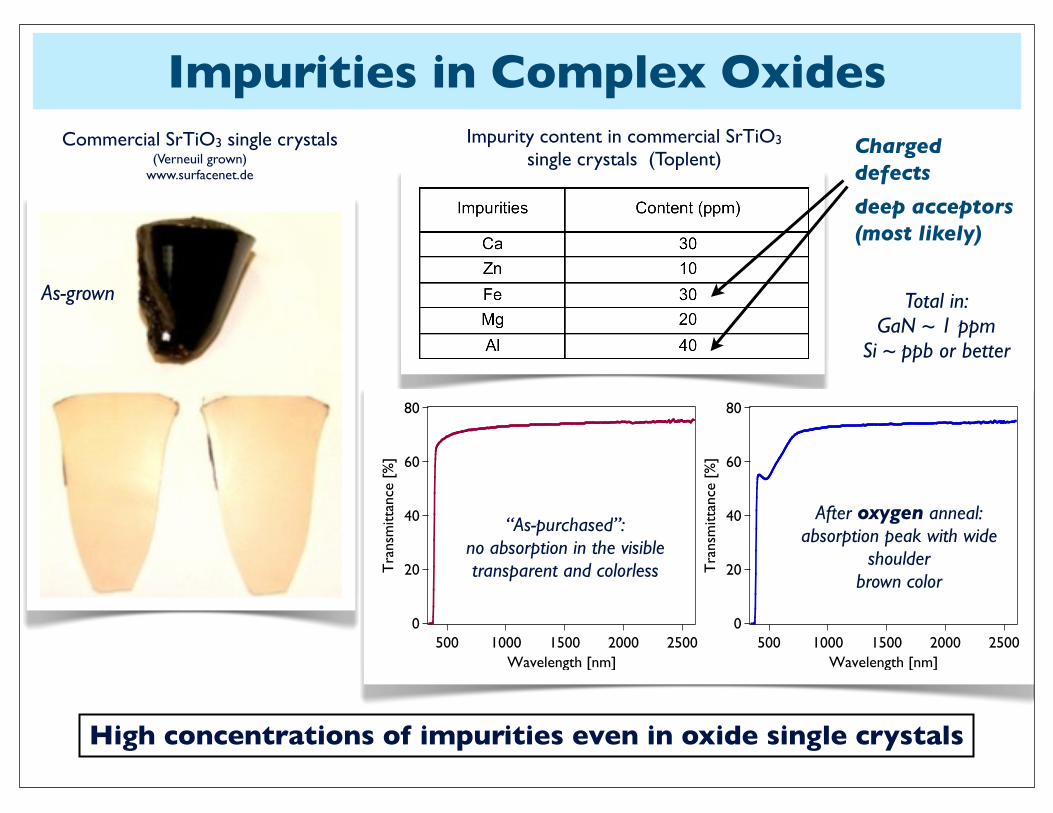
Impurities in Complex OxidesCommercial SrTiO3 single crystals
(Verneuil grown)www.surfacenet.de
Impurity content in commercial SrTiO3 single crystals (Toplent)
Total in:GaN ~ 1 ppm
Si ~ ppb or better
80
60
40
20
0
Tra
nsm
ittan
ce [
%]
2500200015001000500Wavelength [nm]
80
60
40
20
0
Tra
nsm
ittan
ce [
%]
2500200015001000500Wavelength [nm]
“As-purchased”:no absorption in the visibletransparent and colorless
After oxygen anneal:absorption peak with wide
shoulderbrown color
High concentrations of impurities even in oxide single crystals
As-grown
Charged defects
deep acceptors (most likely)

Outline
• Introduction
• Highly-perfect SrTiO3 thin films through stoichiometry control in MBE
• Electrical transport properties of thin film SrTiO3 grown by MBE
• Nature of the 2DEG in delta-doped SrTiO3
• Summary

Oxide Molecular Beam Epitaxy
✓ Low intrinsic defect concentrations:
✓ High purity: evaporation from elemental metals and high purity gases; UHV conditions
✓ Low-energetic deposition
✓ Near-monolayer control of thickness, superlattices, ...
✓ In-situ diagnostics
๏ Stoichiometry control?

Challenges in Oxide MBE
• Low growth pressures
• Oxygen vacancies
• Oxygen vacancies are believed to act as shallow donors in many transition metal oxides
• High oxygen pressures needed during growth
• Metal flux instabilities in the presence of oxygen (oxidation of sources)
Oxygen Stoichiometry
Flux instability of a Ti sublimation source in a background ozone
pressure of 5.0×10⁻⁵ Torr seen in the deposition rate of TiO2
C. D. Theis and D. G. Schlom, J. Vac. Sci. Technol. A 14 (1996), 2677

Challenges in Oxide MBE
Cation Stoichiometry
Temperature (°C)
Temperature (1000/K)
Gas
Pre
ssur
e (T
orr)
GaAs(s) ⇔ Ga(l) + As(g)
4 As(s) ⇔ As4(g)
MBE Growth Window
Temperature (°C)
Below this line, solid As will not precipitate → excess As desorbs in the chamber
4As(s) ⇔ As4(g)
GaAs(s) ⇔ Ga(l) + As(g)
Above this line, As will condense on a Ga-rich GaAs surface
MBE Growth Window
MBE growth window
for GaAs
A wide MBE growth window is largely
responsible for the ease and success of
III-V MBE
C.D. Theis et al., Thin Solid Films 325, 107 (1998).
J. Tsao, Materials Fundamentals of Molecular Beam Epitaxy.

10-27
10-24
10-21
10-18
10-15
10-12
10-9 10
-6
P SrO
(g) [
torr
]
1.00.90.80.70.6
1000/T [1/K]
Challenges in Oxide MBE
Cation Stoichiometry
Temperature (°C)1500 K
SrO(s)⇔ SrO(g)
SrO(g) + TiO2(s) ⇔ SrTiO3(s)
MBE Growth Window
Below this line, solid SrO will not precipitate: SrO will desorb in the chamber*
Above this line, SrO will condense on a TiO-rich SrTiO3 surface*
MBE growth window
for SrTiO3
No MBE growth window for most complex oxides
Assumed a sticking coefficient of one for Ti*
* C.D. Theis et al., Thin Solid Films 325, 107 (1998).

Challenges in Oxide MBE
Additional challenges for the titanates
• Growth rates are limited:
• Very low vapor pressure of Ti
• Typical growth rates:
• < 0.2 nm/min using effusion cell [1,2]
• ≤ 0.7 nm/min using Ti-ball [3]
• (No crucible materials for molten Ti)
• Oxygen causes flux instability for Ti
• High-temperature cells heat substrate
• Higher growth rate with e-beam source but inherent instability of these sources requires flux monitoring and feedback control [4]
Ta crucible
hole in crucible
!"#$%&'%())*%(&+,$%%-&
[1] Z. Yu et. al., Thin Solid Films 462-463,51 (2004)[2] P. Fisher et. al., J. Appl. Phys. 103, 013519 (2008)[3] M.D. Biegalski et.al., J. Appl. Phys. 104, 114109 (2008)[4] M. Naito et.al., Physica C 305, 233 (1998); S. A. Chambers, Surf. Sci. Reports 39, 105 (2000)

Novel Oxide MBE Approach
Bubbler
Gas supply (heated)
Leak valve
Baratron
Titanium tetra isopropoxide (TTIP)

Hybrid Oxide MBETitanium tetra iso propoxide (TTIP)
Ti
OTTIP source
• TTIP has orders of magnitude higher vapor pressures than solid Ti
• Scalable growth rate and stable flux
• No flux instabilities in presence of oxygen: higher oxygen pressure can be used
• Ti already comes bonded to four oxygens → improved oxygen stoichiometry
Ti(OC3H7)4 → TiO2 + 2 C3H7OH + 2 C3H6
@ T = 350˚C
Sr cellOxygen plasma
source
!!"#$!%&'()($
*+,-./&()($
012(3$
4-,3%,1)%&$56(2%)($
78$9:(*8$;%68+$<=4=$>?@<4A$B$CCC8D-%:(86%*EF,GH121$

Metal-Organic MBE of Rutile TiO2
Ts ≈ 615 °CTTIP beam flux: 2×10⁻⁶ torr
No oxygen
• Single crystalline rutile (101) TiO2 on r-plane sapphire even without any additional oxygen
• TTIP source supplies oxygen
• Scalable growth rates as high as 125 nm/hr
B. Jalan, R. Engel-Herbert, J. Cagnon, S. Stemmer, J. Vac. Sci.
Technol. A 27, 230 (2009).
TTIP source
Al2O3!
TiO2!

Hybrid MBE of SrTiO3
TTIP sourceoxygen plasma source
Sr source
Tsub= 800 °Cpox= 8 × 10⁻⁶ torr
55.4
53.3
42.1
41.0
39.5
TTIP / Srflux ratio
B. Jalan, R. Engel-Herbert, N. J. Wright, S. Stemmer, J. Vac. Sci. and Technol. A 27, 461 (2009). B. Jalan, P. Moetakef, S. Stemmer, Appl. Phys. Lett. 95, 032906 (2009).
• Co-deposition (not shuttered)
• Lattice parameter as a measure of stoichiometry
• Lattice parameter increases for non-stoichiometry films (Sr rich and Ti rich)
• Excellent control over film stoichiometry
SrTiO3!
SrTiO3!

Hybrid MBE of SrTiO3: Growth Modes
after growth
substrate
• Persistent (> 180) RHEED oscillations indicate layer-by-layer growth mode [only been reported for a few systems: Si, Pt, AlAs]
• Transition to step-flow growth
• Streaky RHEED indicates atomically smooth film surface
• Surface reconstructions
• 2× along [110] (always); 4× along [110] (only for stoichiometric films after growth)
• Further investigations are required to understand origin of persistent RHEED oscillations.
B. Jalan, R. Engel-Herbert, N. J. Wright, S. Stemmer, J. Vac. Sci. and Technol. A 27, 461 (2009). B. Jalan, P. Moetakef, S. Stemmer, Appl. Phys. Lett.
95, 032906 (2009).
SrTiO3!
SrTiO3!

Hybrid MBE of SrTiO3
LSAT = (La0.3Sr0.7)
(Al0.65Ta0.35)O3
XRD rocking curve
AFM
B. Jalan, R. Engel-Herbert, N. J. Wright, S. Stemmer, J. Vac. Sci. and Technol. A 27, 461 (2009). B. Jalan, P. Moetakef, S. Stemmer, Appl. Phys. Lett. 95, 032906 (2009).
• LSAT* substrates for rocking curve measurements
• On LSAT substrates, narrow rocking curve widths, similar to that of substrate (34 arcsec)
• Atomically smooth film surfaces on all substrates
LSAT!
SrTiO3!
DyScO3!
SrTiO3!

MBE Growth Window
TTIP desorption leads to a growth window at practical substrate temperatures and fluxes
Stoichiometry is self-regulating within the growth window
No need for precise flux control
Shift to higher TTIP/Sr flux ratios with increasing temperatures shows that desorption of TTIP is responsible for growth window
Growth windowsGrowth windows
B. Jalan, P. Moetakef, S. Stemmer, Appl. Phys. Lett. 95, 032906 (2009).
SrTiO3!
SrTiO3!

Significance of the MBE Growth Window
B. Jalan, P. Moetakef, S. Stemmer, Appl. Phys. Lett. 95, 032906 (2009).
• Without an MBE growth window, stoichiometry control requires precise flux control
• Only possible to 0.1 - 1 % *,*** M. E. Klausmeier-Brown, J. N. Eckstein, I. Bozovic, and G. F. Virshup, Appl. Phys. Lett. 60, 657 (1992). ** J. H. Haeni, C. D. Theis, and D. G. Schlom, J. Electroceram. 4, 385 (2000).
• Corresponds to defect concentrations of 1020-1021 cm-3
• Conventional MBE with all solid sources for Sr and Ti does not have a growth window.
• Hybrid MBE approach with TTIP: desorption leads to a growth window at practical substrate temperatures and fluxes.
• Stoichiometry is self-regulating within the growth window, no need for precise flux control.
• Volatility of TTIP is the reason for the growth window.

Outline
• Introduction
• Highly-perfect SrTiO3 thin films through stoichiometry control in MBE
• Electrical transport properties of thin film SrTiO3 grown by MBE
• Nature of the 2DEG in delta-doped SrTiO3
• Summary

Electrical Transport Properties
Hall Mobilities - SrTiO3 Single Crystals
O. N. Tufte, P. W. Chapman, Phys. Rev. 155, 796 (1967)
1967 2007
G. Herranz et al., Phys. Rev. Lett. 98, 21603 (2007)
Hal
l m
ob
ilit
y (
cm2/V
s)
Hal
l m
ob
ilit
y (
cm2/V
s)
Hal
l m
ob
ilit
y (
cm2/V
s)
Temperature (K)
Temperature (K)
Temperature (K)
A. Spinelli et al., Phys. Rev. B 81, 155110 (2010)
μ = 22,000 cm2/Vs at n = 1.4×1017cm-3
2010
μ = 25,000 cm2/Vs
μ = 22,100 cm2/Vs at n = 8×1017cm-3
10 100
n-type dopants: VO
.. or Nb

Electrical Transport Properties
1018
2
4
1019
2
4
1020
2
Car
rier
con
cent
ratio
n [c
m-3
]
1018
1019
1020
La concentration [cm-3
]
J. Son, P. Moetakef, B. Jalan, O. Bierwagen, N. J. Wright, R. Engel-Herbert, S. Stemmer, Nature Mater. 9, 482 (2010).
• 1:1 correspondence of La-concentration and free carrier concentration over several orders of magnitude
• Excellent control over doping → concentration of unintentional defects below doping level
• Metallic (degenerate) for all doping levels
SrTiO3!
SrTiO3!
La:SrTiO3!Doping of MBE SrTiO3 with La
1017
2
4
6
1018
2
4
6
1019
Car
rier
con
cent
ratio
n [c
m-3
]
300250200150100500
Temperature [K]
STO 1 STO 2 STO 3

La-Doping of SrTiO3
SrTiO3!
SrTiO3!
La:SrTiO3!HAADF/STEM
La atoms
Interface
La-doped SrTiO3
nHall = 1.8×1021 cm-3
undoped SrTiO3 buffer layer
Electrical Transport Properties
101
102
103
104
105
Ele
ctro
n m
obili
ty [
cm2 /V
s]
2 3 4 5 610
2 3 4 5 6100
2 3
Temperature [K]
4.0
3.0
2.0
1.054321
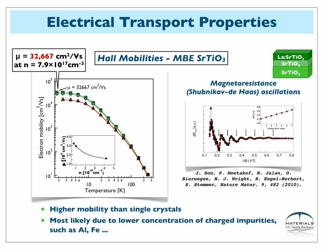
µ = 32667 cm2/Vs
n [1018
cm-3
]
µ [
10
4 cm
2 /Vs]
Hall Mobilities - MBE SrTiO3μ = 32,667 cm2/Vs at n = 7.9×1017cm-3
J. Son, P. Moetakef, B. Jalan, O. Bierwagen, N. J. Wright, R. Engel-Herbert, S. Stemmer, Nature Mater. 9, 482 (2010).
SrTiO3!
SrTiO3!
La:SrTiO3!
Magnetoresistance(Shubnikov-de Haas) oscillations
• Higher mobility than single crystals
• Most likely due to lower concentration of charged impurities, such as Al, Fe ...

Electrical Transport Properties
Seebeck Coefficients - MBE SrTiO3
S = 980 µVK-1
• Seebeck coefficient comparable to bulk SrTiO3
• Large thermoelectric power factor of 39 µW/cmK2
• Comparable to commercial thermoelectrics
€
ZT =S2σκ
TSrTiO3!
SrTiO3!
La:SrTiO3!
300 K
300 K
10-1
100
101
102
103
104
σ [
Scm
-1]
1017
1018
1019
1020
1021
1022
n [cm-3
]
1000
800
600
400
200
0
|S| [
µVK
-1]
|S|, film (this work)|S|, single crystal (Okuda et al.)|S|, single crystal (Frederikse et al.)σ, film (this work)σ, single crystal (Okuda et al.)
40
30
20
10
0
S2 σ [µ
W/c
mK
2 ]
1017
1018
1019
1020
1021
1022
n [cm-3
]
B. Jalan, S. Stemmer, Appl. Phys. Lett. 97, 042106 (2010).

Outline
• Introduction
• Highly-perfect SrTiO3 thin films through stoichiometry control in MBE
• Electrical transport properties of thin film SrTiO3 grown by MBE
• Nature of the 2DEG in delta-doped SrTiO3
• Summary

Two-dimensional electron gases with SrTiO3
*Y. Kozuka et al., Nature 462, 487 (2009).
• Delta-doping: thin highly doped layer sandwiched between undoped layers
• Shubnikov-de Haas oscillations and 2DEG behavior have been observed*
delta-doped layer
SrTiO3
SrTiO3
Ener
gy
Depth
EF
E0
E1
E2
• Know the origin of the carriers (unlike LAO/STO)
• Potential well and subband formation
• Electrons in highest subbands are spread-out and have higher mobility
• Significant scatter from the dopants; however, it allows for the study of 2DEGs

Two-dimensional electron gas in delta-doped SrTiO3
• Only perpendicular component of B-field determines SdH → 2D
• Fourier transform indicates two frequencies → two subbands or is this something else?
MBE film, La-delta doped layerShubnikov-de Haas oscillations
FT a
mpl
. (a.
u.)
100806040200
Frequency (T)
27 T54 T
! R
xx
[a.u
.]
0.240.200.160.120.08
1/B [ T-1]
0.410 K 0.8 K 1.2 K 1.8 K 2.5 K 3.0 K
B. Jalan, S. Stemmer, S. Mack, S. J. Allen, Phys. Rev. B 82, 081103(R)(2010).
SrTiO3
SrTiO3
La:SrTiO3

Two-dimensional electron gas in delta-doped SrTiO3
Fourier transform indicates two frequencies → two subbands?
FT a
mpl
. (a.
u.)
100806040200
Frequency (T)
27 T54 T SrTiO3
SrTiO3
La:SrTiO3
B. Jalan, S. Stemmer, S. Mack, S. J. Allen, Phys. Rev. B 82, 081103(R)(2010).
!Rxx
[a.u
.]0.240.200.160.120.08
1/B [ T-1
]
Experiment Two subband model
• Experiment fit to standard 2DEG equation with two subbands [1]:
• Use experimentally determined electron mass (1.56 m0)
• The frequencies (21 and 54 T) do not correspond to the experimental frequencies
• The SdH oscillations are not well-matched
[1] A. Isihara, and L. Smrcka, J. Phys. C 19, 6777 (1986).
!
"Rxx
= 4R0 exp #2s$ 2k
BT
D/!%
c( )s=1
&
'2s$ 2
kBT !%
c
sinh 2s$ 2k
BT /!%
c( )cos
2$s "1 B( )B
#$s
(
) * *
+
, - - !
!
"c
= eB m#!
?

Two-dimensional electron gas in SrTiO3
Analogy with hole 2DHGs in III-V
quantum well potential lifts k=0 degeneracy
Anti-crossing
Need to also consider strong non-parabolicity:
C. Weisbuch, B. Vinter: Quantum Semiconductor Structures
D. A. Broido, and L. J. Sham, Phys. Rev. B 31, 888 (1985).
U. Ekenberg, and M. Altarelli, Phys. Rev. B 32, 3712 (1985).
• Degeneracy of VB and surface electric field combine to couple strongly to parallel and perpendicular transport → highly non-parabolic subbands → field-dependent cyclotron mass
• Lifting of two-fold spin degeneracy due to lack of interface inversion symmetry and strong spin-orbit coupling → two distinct subbands

Two-dimensional electron gas in delta-doped SrTiO3
• Nevertheless, realize the following (in analogy with hole gases in III-V):
• The effective mass (~ 1-2 m0) and effective Landé factor, g, (~2) are comparable
• Landau and spin splittings in the magnetic field are likely comparable
• Cannot use equation with g = 0
• Use model with one subband + spin splitting.
• Lack of understanding of the bulk electronic structure of SrTiO3:
• Tetragonal splitting (how large?)
• Spin-orbit split off band (how much?)
➡ Experiments needed!
➡Theory quite complicated

Two-dimensional electron gas in delta-doped SrTiO3
B. Jalan, S. Stemmer, S. Mack, S. J. Allen, Phys. Rev. B 82, 081103(R)(2010).
• Use three-dimensional equation [1], because it includes spin-splitting (applicable here because of weakness of the oscillations):
[1] L. M. Roth, and P. N. Argyres, in Semiconductors and Semimetals Vol. 1, edited by R. K. Williardson, and A. C. Beer (Academic Press, New York, 1966).
!
"Rxx
R0
=5
2b
s
s=1
#
$ cos2%E
F
!&c
s '%
4
(
) *
+
, - !
!
2"nh
2eB!
two-dimensional case
!
bs ="1( )
s
s
!#c
2EF
$
% &
'
( )
1 2
2* 2skBT !#c
sinh 2* 2skBT !#c( )+ exp "
2* 2skBTD
!#c
$
% &
'
( ) cos
*sgm,
2me
$
% &
'
( ) !
relative strength of weak and strong
minima
SdH periodicity
s = 1,2
TD, R0, g, period (Δ1/B) as fit parameters to data at 0.4 K
!
"1 B = 2e nh( )
One subband + spin splitting model
temperature dependence is
determined by m*

Two-dimensional electron gas in delta-doped SrTiO3
B. Jalan, S. Stemmer, S. Mack, S. J. Allen, Phys. Rev. B 82, 081103(R)(2010).
0.250.200.150.101/B (T
-1)
0.41 K 0.8 K 1.2 K 1.8 K 2.5 K 3.0 K
! R
xx (
a.u.
)
Experiment
Calculation
• Fit to 0.4 K data yields experimentally determined frequency (27 T)
• Temperature dependence and SdH period is well described
• Only the highest lying subband, with the highest mobility, gives rise to SdH
• Spin-related effects important
• Series of possible g factors: 0.698, 1.86, ...
One subband + spin splitting model
• Carrier concentration is 1.3×1012cm-2, about 4% of the Hall concentration (3×1013cm-2).
• A small fraction of the electrons in one subband in a large number of electrons in the delta-doping potential
• The electron density in that subband is likely not constant (note different frequencies at low B-fields) in exp. and calc.

Summary• Novel oxide MBE approach allows for high purity, low-energetic
deposition of complex oxides (titanates) with excellent stoichiometry control
• MBE growth window allows for stoichiometric films without being limited by precision of flux control
• Low carrier concentrations (~1017 cm-3) and 1:1 correspondence of dopant and carrier concentrations indicate low intrinsic defect concentrations
• Very low defect concentrations allow for record electron mobilities
• 2DEG in SrTiO3 obtained through delta-doping exhibits 2D quantum oscillations
• 2DEGs in SrTiO3 contain all the complications of 2DHGs of conventional semiconductors
• Showed that quantitative description of DEGs in SrTiO3 can be obtained provided effects from spin-splitting are taken into account
• Spin-related effects are important in DEGs in SrTiO3