tutorial post-silicon validation in the soc era: a ... · tutorial post-silicon validation in the...
TRANSCRIPT

68 2168-2356/17 © 2017 IEEE Copublished by the IEEE CEDA, IEEE CASS, IEEE SSCS, and TTTC IEEE Design&Test
Tutorial
Post-Silicon Validation in the SoC Era: A Tutorial Introduction
Digital Object Identifier 10.1109/MDAT.2017.2691348
Date of publication: 5 April 2017; date of current version:
4 May 2017.
Prabhat MishraUniversity of Florida
Computing deviCes pervade our everyday life. In addition to traditional desktops and lap-tops, we have in the past decade already seen the emergence and ubiquity of handheld devices such as smartphones and tablets. Today, we are in the midst of a further explosive proliferation of com-puting fueled by the Internet of things (IOT) [1], where computing devices equipped with sensors, integrated electronics, and sophisticated software are attached to physical objects of “things” to make them smart and adaptable to their environment. For instance, highly complex computing systems are now attached to wearables (e.g., watches, fitness trackers, ear buds), household items (e.g., ceiling fans, light bulbs, refrigerators), and automobiles, all
connected to the Internet and coordi-nating and communicating to provide smart, immersive, and transformative user experiences. We anticipate an estimated 50 billion smart, connected computing devices by 2020 from a “mere” 500 million in 2003 [2], with estimates of trillions within the next decade, representing the fastest growth for any sector in our entire history.
Modern embedded computing devices are generally architected
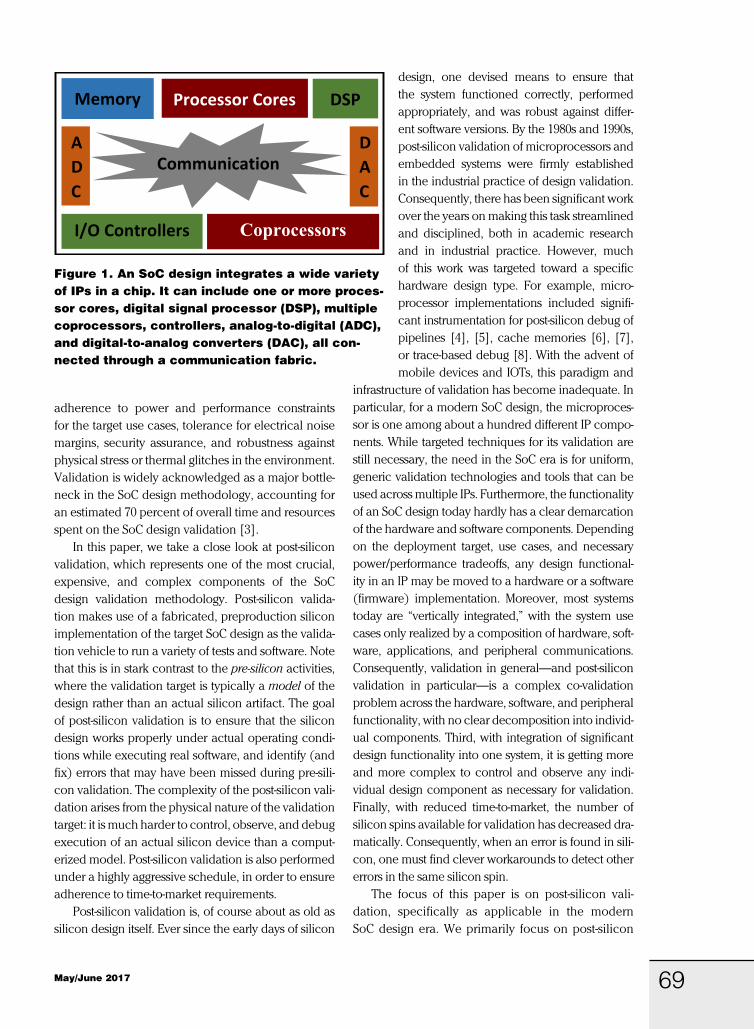
through a system-on-chip (SoC) design paradigm. An SoC architecture includes a number of prede-signed hardware blocks (potentially augmented with firmware and software as well) of well-defined functionality, often referred to as “intellectual prop-erties” or “IPs.” These IPs communicate and coor-dinate with each other through a communication fabric or network-on-chip (NoC). Figure 1 shows the major IPs in a typical SoC design. The idea of SoC design is to quickly configure these predesigned IPs for the target use cases of the device and connect them through standardized communication inter-faces, enabling rapid design turnaround time for new applications and market segments.
Given the diversity of critical applications of com-puting devices in the new era, as well as the complex-ity of the devices itself, their validation is clearly a crucial and challenging problem. Validation includes a host of tasks, including functional correctness,
Ronny Morad and Avi ZivIBM
Editor’s note:Post-silicon validation is a complex and critical component of a modern system-on-chip (SoC) design verification. It includes a large number of inter-related activities each with its own nuance and subtleties, requires extensive planning, and spans the entire system design lifecycle. This article provides a comprehensive high-level overview of the various facets of post-silicon validation, and includes industrial case studies illustrating their real-life application.
—Swarup Bhunia, University of Florida
Sandip RayNXP Semiconductors
69May/June 2017
adherence to power and performance constraints for the target use cases, tolerance for electrical noise margins, security assurance, and robustness against physical stress or thermal glitches in the environment. Validation is widely acknowledged as a major bottle-neck in the SoC design methodology, accounting for an estimated 70 percent of overall time and resources spent on the SoC design validation [3].
In this paper, we take a close look at post-silicon validation, which represents one of the most crucial, expensive, and complex components of the SoC design validation methodology. Post-silicon valida-tion makes use of a fabricated, preproduction silicon implementation of the target SoC design as the valida-tion vehicle to run a variety of tests and software. Note that this is in stark contrast to the pre-silicon activities, where the validation target is typically a model of the design rather than an actual silicon artifact. The goal of post-silicon validation is to ensure that the silicon design works properly under actual operating condi-tions while executing real software, and identify (and fix) errors that may have been missed during pre-sili-con validation. The complexity of the post-silicon vali-dation arises from the physical nature of the validation target: it is much harder to control, observe, and debug execution of an actual silicon device than a comput-erized model. Post-silicon validation is also performed under a highly aggressive schedule, in order to ensure adherence to time-to-market requirements.
Post-silicon validation is, of course about as old as silicon design itself. Ever since the early days of silicon
design, one devised means to ensure that the system functioned correctly, performed appropriately, and was robust against differ-ent software versions. By the 1980s and 1990s, post-silicon validation of microprocessors and embedded systems were firmly established in the industrial practice of design validation. Consequently, there has been significant work over the years on making this task streamlined and disciplined, both in academic research and in industrial practice. However, much of this work was targeted toward a specific hardware design type. For example, micro-processor implementations included signifi-cant instrumentation for post-silicon debug of pipelines [4], [5], cache memories [6], [7], or trace-based debug [8]. With the advent of mobile devices and IOTs, this paradigm and
infrastructure of validation has become inadequate. In particular, for a modern SoC design, the microproces-sor is one among about a hundred different IP compo-nents. While targeted techniques for its validation are still necessary, the need in the SoC era is for uniform, generic validation technologies and tools that can be used across multiple IPs. Furthermore, the functionality of an SoC design today hardly has a clear demarcation of the hardware and software components. Depending on the deployment target, use cases, and necessary power/performance tradeoffs, any design functional-ity in an IP may be moved to a hardware or a software (firmware) implementation. Moreover, most systems today are “vertically integrated,” with the system use cases only realized by a composition of hardware, soft-ware, applications, and peripheral communications. Consequently, validation in general—and post-silicon validation in particular—is a complex co-validation problem across the hardware, software, and peripheral functionality, with no clear decomposition into individ-ual components. Third, with integration of significant design functionality into one system, it is getting more and more complex to control and observe any indi-vidual design component as necessary for validation. Finally, with reduced time-to-market, the number of silicon spins available for validation has decreased dra-matically. Consequently, when an error is found in sili-con, one must find clever workarounds to detect other errors in the same silicon spin.
The focus of this paper is on post-silicon vali-dation, specifically as applicable in the modern SoC design era. We primarily focus on post-silicon
Figure 1. An SoC design integrates a wide variety of IPs in a chip. It can include one or more proces-sor cores, digital signal processor (DSP), multiple coprocessors, controllers, analog-to-digital (ADC), and digital-to-analog converters (DAC), all con-nected through a communication fabric.

70 IEEE Design&Test
Tutorial
functional validation techniques, although we pro-
vide rough overviews of some of the other categories,
viz., electrical and marginality. The SoC validation
challenges outlined above have resulted in a num-
ber of architectures, infrastructures, test and CAD
flows, and so on. However, they are not utilized in
a top-down, disciplined manner. In fact, tools, flows,
and design instrumentations have been incremen-
tally accumulated over time in response to specific
challenges or requirements. Today, over 20 percent
of the design real estate and a significant component
of the CAD flow effort are devoted toward silicon val-
idation. It is nontrivial to transform or mold the archi-
tecture for specific device use cases. In addition to
providing a survey of the various facets of silicon val-
idation, our goal is to deconstruct this complexity,
facilitate understanding of the rationale for many of
the available flows and architectures, and illustrate
experiences in post-silicon validation for real indus-trial examples.
Figure 2 shows three stages of SoC validation: pre-silicon validation, post-silicon validation, and on-field debug. The figure also shows some of the important activities associated with the different stages. The remainder of the paper describes the major tasks relevant for post-silicon and debug. The first section reviews the spectrum of validation activi-ties from pre-silicon through post-silicon and on-field survivability. The next section gives a flavor of the diverse range of activities involved in post-silicon validation, while the “Silicon validation challenges” section discusses some of the high-level challenges. The next section focuses on post-silicon planning, that is, the pre-silicon activities targeted toward facil-itating and streamlining post-silicon validation. In the “Trace signal selection” and “Test generation” sections, we delve into some details on two aspects of this planning, signal selection, and test genera-tion. The next section discusses an industrial post-sil-icon validation experience, with IBM Power8, and the conclusion is drawn in the final section.
The validation spectrumWe can roughly divide validation activities into
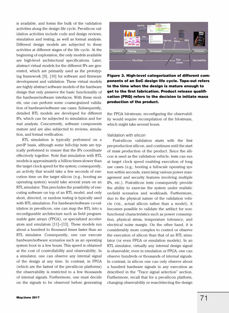
three components: pre-silicon, post-silicon, and on-field survivability. To understand the different post-silicon activities involved, it is crucial to com-prehend the position it holds among validation activities across different phases of SoC design and development. Indeed, validation is best viewed as a “continuum” of activities using artifacts with increas-ing levels of maturity. As we move from pre-silicon to post-silicon and finally on-field execution, more and more complex usage scenarios are exercised poten-tially stimulating errors that could not be seen in previous validation phases. At the same time, observ-ability and controllability of the design during these executions get progressively more complex making it harder to root-cause a failure. At the same time, the cost of a bug increases and the time available for debug decreases as we go further into the system life cycle. In this section, we provide a high-level over-view of this continuum of validation activities. The timeline for these activities is shown in Figure 3.
Pre-silicon activitiesPre-silicon validation refers to all of the vali-
dation activities performed before the first silicon
Figure 2. Three important stages of SoC validation: pre-silicon validation, post-silicon validation, and on-field survivability.
71May/June 2017
is available, and forms the bulk of the validation activities along the design life cycle. Pre-silicon val-idation activities include code and design reviews, simulation and testing, as well as formal analysis. Different design models are subjected to these activities at different stages of the life cycle. At the beginning of exploration, the only models available are high-level architectural specifications. Later, abstract virtual models for the different IPs are gen-erated, which are primarily used as the prototyp-ing framework [9], [10] for software and firmware development and validation. These virtual models are highly abstract software models of the hardware design that only preserve the basic functionality of the hardware/software interfaces. With these mod-els, one can perform some coarse-grained valida-tion of hardware/software use cases. Subsequently, detailed RTL models are developed for different IPs, which can be subjected to simulation and for-mal analysis. Concurrently, software components mature and are also subjected to reviews, simula-tion, and formal verification.
RTL simulation is typically performed on a per-IP basis, although some full-chip tests are typ-ically performed to ensure that the IPs coordinate effectively together. Note that simulation with RTL models is approximately a billion times slower than the target clock speed for the system; consequently, an activity that would take a few seconds of exe-cution time on the target silicon (e.g., booting an operating system) would take several years on an RTL simulator. This precludes the possibility of exe-cuting software on top of an RTL model, and only short, directed, or random testing is typically used with RTL simulation. For hardware/software co-val-idation in pre-silicon, one can map the RTL into a reconfigurable architecture such as field program-mable gate arrays (FPGA), or specialized acceler-ators and emulators [11]–[13]. These models run about a hundred to thousand times faster than an RTL simulator. Consequently, one can execute hardware/software scenarios such as an operating system boot in a few hours. This speed is obtained at the cost of controllability and observability. In a simulator, one can observe any internal signal of the design at any time. In contrast, in FPGA (which are the fastest of the pre-silicon platforms) the observability is restricted to a few thousands of internal signals. Furthermore, one must decide on the signals to be observed before generating
the FPGA bit-stream; reconfiguring the observabil-ity would require recompilation of the bit-stream, which might take several hours.
Validation with siliconPost-silicon validation starts with the first
pre-production silicon, and continues until the start of mass production of the product. Since the sili-con is used as the validation vehicle, tests can run at target clock speed enabling execution of long use cases (e.g., booting a full-scale operating sys-tem within seconds, exercising various power man-agement and security features involving multiple IPs, etc.). Post-silicon tests consequently provide the ability to exercise the system under realistic on-field scenarios and workloads. Furthermore, due to the physical nature of the validation vehi-cle (viz., actual silicon rather than a model), it becomes possible to validate the artifact for non-functional characteristics such as power consump-tion, physical stress, temperature tolerance, and electrical noise margin. On the other hand, it is considerably more complex to control or observe the execution of silicon than that of an RTL simu-lator (or even FPGA or emulation models). In an RTL simulator, virtually any internal design signal is observable; even in emulation or FPGA, one can observe hundreds or thousands of internal signals. In contrast, in silicon one can only observe about a hundred hardware signals in any execution as described in the “Trace signal selection” section. Furthermore, recall that for a pre-silicon platform, changing observability or rearchitecting the design
Figure 3. High-level categorization of different com-ponents of an SoC design life cycle. Tape-out refers to the time when the design is mature enough to get to the first fabrication. Product release qualifi-cation (PRQ) refers to the decision to initiate mass production of the product.

72 IEEE Design&Test
Tutorial
to facilitate more control would at most require a recompilation (although recompilation is non-trivial and may take several hours); however, for silicon, it requires silicon respin (i.e., redesign, val-idate again, and expensive refabrication). Indeed, most of the critical challenges in post-silicon vali-dation stem from observability and controllability constraints, and we discuss these challenges in the “Silicon validation challenges” section.
To underline the criticality of post-silicon, it is important to note the factors contributing to the aggressive debug timeline requirements and the high cost of bug (and bug escape) in post-silicon validation. Post-silicon validation is the final vali-dation activity before mass production is initiated. The timeline for beginning mass production is gov-erned by several factors many of which are dictated by market economics, e.g., the need for launching a product to align with winter holiday shopping or back-to-school timeframe. Missing such a window may mean millions to billions of dollars of loss in revenue, and in some cases missing the market for the product altogether. The decision to move for-ward with mass production or cancel the product altogether (referred to as the “PRQ” call) is made based on the trend and type of bugs found during post-silicon, results of power-performance valida-tion, tolerance of the product to target noise mar-gins, and electrical variations, all of which depend critically on post-silicon validation. Consequently, post-silicon validation must enable aggregation of substantial trending data on design bugs as well as nonfunctional characteristics to enable a decision on product launch (and hence mass production). Note that the launch timeframe is typically deter-mined a long time (even years) in advance based on target market forecast for the product and changes can result in substantial economic repercussions. Consequently, the post-silicon activity must per-form high-quality validation within the limited and fixed timeframe (between first silicon and PRQ) to ensure a marketable product: delay in post-sili-con can risk a product cancellation resulting in a loss of the entire investment on the product from architecture to validation, or in launching a prod-uct that malfunctions on-field in ways not covered by on-field survivability architectures (see below), resulting in loss of millions to billions of dollars in revenue due to product recall, impact on company reputation, etc.
Survivability and on-field debugSurvivability refers to the validation and debug
activities employed on a system or device to mit-igate errors or malfunctions observed during on-field execution. One may argue that survivabil-ity is not a validation activity at all, since it happens on-demand at deployment sites, rather than with following a preplanned schedule as for other vali-dation activities. Nevertheless, it is still considered in concert with validation activities, since many of the technologies used in survivability bear a strong resemblance to post-silicon validation. In particular, survivability activities depend on design-for-debug (DfD), that is, hardware features introduced specif-ically to facilitate debug and validation of silicon. Most mitigation techniques employed for surviva-bility involve “patching” or reconfiguring the func-tionality of the system through software or firmware updates. Note that in order to successfully patch design functionality, the design itself must include significant configurability options. Furthermore, once an error or vulnerability is discovered on-field, the time available for developing a mitigation or workaround strategy is extremely short. One reason for the short time availability is that many of the errors might be exploited as security vulnerabilities which, once detected and advertised on-field, can be exploited for malicious purposes; it is important to repair such vulnerabilities before a catastrophic exploitation is performed. Even if the error is not catastrophic, on-field problems can get significant (negative) limelight, causing damage to the com-pany reputation, which may result in significant revenue loss. On the other hand, it may be a highly creative process to identify a patching strategy to mitigate on-field problems. In particular, the ability to patch a design depends on how much configur-ability and controllability have been built into the system to enable the patch. Developing complex system designs with a flexible, configurable archi-tecture is one of the crucial challenges in the SoC era, and we will describe it in the context of plan-ning for post-silicon validation in the “Planning for post-silicon readiness” section.
Overview of post-silicon activitiesPost-silicon validation includes a number of dif-
ferent activities including validation of both func-tional and timing behavior as well as nonfunctional requirements. Each validation activity entails its own

73May/June 2017
challenge and includes techniques, tools, and meth-odologies to mitigate them. In this section, we dis-cuss a few of these activities, to give a flavor of their range and diversity.
Power-on-debug: One of the first activities per-formed when a preproduction silicon arrives at a post-silicon laboratory for the first time is to power it on. Powering on the device is actually a highly complex activity. If the device does not power on, the on-chip instrumentation architecture (see below) is typically not available, resulting in extremely limited (often zero) visibility into the design internals. This makes it difficult to diag-nose the problem. Consequently, power-on debug includes a significant brainstorming component. Of course, some visibility and controllability still exist even at this stage. In particular, power-on debug typically proceeds with a custom “debug board,” which provides a higher configurability and fine-grained control over a large number of different design features. The debug activity then entails coming up with a bare-bone system config-uration (typically removing most of the complex features, e.g., power management, security, and software/firmware boot mechanisms,), which can reliably power on. Typically, starting from the time the silicon first arrives at the laboratory, obtaining a stable power-on recipe can take a few days to a week. Once this is achieved, the design is recon-figured incrementally to include different complex features. At this point, some of the internal DfD features are available to facilitate this process. Nev-ertheless, it is still a highly challenging enterprise and can take several weeks to achieve. Note that as designs become more and more configurable, the process of defeaturing and refeaturing for pow-er-on debug can get increasingly harder. Once the power-on process has been stabilized, a number of more complex validation and debug activities can be initiated.
Basic hardware logic validation: The focus of the logic validation is to ensure that the hardware design works correctly, and exercise specific fea-tures of constituent IPs in the SoC design. This is typically done by subjecting the silicon to a wide variety of tests that include both focused tests for exercising specific features as well as random and constrained-random tests. Traditionally, the SoC is
placed on a custom platform (or board) designed specifically for debug with specialized instrumen-tation for achieving additional observability and controllability of internals of different IPs. Signifi-cant debug software is also developed to facilitate this testing (see below). Note that these tests are different from system-level directed tests. In par-ticular, tests executed for post-silicon validation are system-level, involving multiple IPs and their coordination.
Hardware/software compatibility validation: Compat-ibility validation refers to the activities to ensure that the silicon works with various versions of systems, application software, and peripherals. The valida-tion accounts for various target use cases of the sys-tem, the platforms in which the SoC is targeted to be included, etc. Compatibility validation includes, among others, the following:
• validation of system usage with add-on hardware of multiple external devices and peripherals;
• exercising various operating systems and appli-cations (including multimedia, games, etc.);
• use of various network protocols and communi-cation infrastructures.
In addition to the generic complexities of post-sil-icon validation (see below), a key challenge here is the large number of potential combinations (of configurations of hardware, software, peripheral, and use cases) that need to be tested. It is com-mon for compatibility validation to include over a dozen operating systems of different flavors, more than a hundred peripherals, and over 500 applications.
Electrical validation: Electrical validation exercises electrical characteristics of the system, compo-nents, and platform to ensure adequate electrical margin under worst-case operating conditions. Here “electrical characteristics” include input–out-put, power delivery, clock, and various analog/mixed-signal (AMS) components. The validation is done with respect to various specification and plat-form requirements, e.g., input–-output validation uses the platform quality and reliability targets. As with compatibility validation above, a key challenge here is the size of the parameter space: for system quality and reliability targets, the validation must cover the entire spectrum of operating conditions (e.g., voltage, current, and resistance) for millions of
74 IEEE Design&Test
Tutorial
parts. The current state of practice in electrical vali-dation is an integrated process of the following:
• sampling the system response for a few sample parts;
• identifying operating conditions under which the electrical behavior lies outside specification;
• optimization, redesign, and tuning as necessary to correct the problem.
Note that unlike the logic and compatibility valida-tion above, electrical validation must account for statistical variation of the system performance and noise tolerance across different process corners. PRQ requires the average defect to be low, typically less than 50 parts per million.
Speed-path validation: The goal of speed-path valida-tion is to identify frequency-limiting design paths in the hardware. Because of variations, the switching performance of different transistors in the design var-ies. This leads to data being propagated at different rates along different circuit paths. The speed at which the circuit can perform is ultimately constrained by the limitations of the slowest (in terms of data prop-agation speed) path in the design. Identifying such slow paths is therefore crucial in optimizing the design performance. Speed path analysis includes identifica-tion of both a potentially slow transistor, among mil-lions or billions of them in a design, responsible for the speed path; and the execution cycle (over a test, potentially millions of cycles long) that causes a slow transition. Speed path debug makes use of a number of technologies, including specialized testers, Shmoo (2-D plot) of chip failure pattern over the voltage and frequency axes, DfD instrumentation available for observability, as well as laser-assisted observation of design internals [14] and techniques for stretch-ing and shrinking clock periods [15]. More recently, analysis techniques based on formal methods have been successfully used for speed-path identification [16], [17]. In spite of these latest developments, a significant ingenuity is necessary to isolate frequency limiting paths for modern designs.
Obviously, the above list of activities is not exhaus-tive. In addition to the above, validation covers the behavior of the system under extreme temperatures, physical stress, etc. Even the categories themselves are not “cast in stone”: post-silicon validation in prac-tice typically involves close collaboration among val-idators of all the different areas. As an example, with
increasingly tightening hardware/software integration in modern SoC designs, the boundary between basic hardware logic validation and compatibility validation with software has become blurred. In many cases, it is impossible to validate the hardware standalone with-out also considering (at least) the firmware running on the different IP cores. Indeed, post-silicon functional validation today often refers to the union of logic and compatibility validation.
Silicon validation challengesPost-silicon validation and debug clearly involve
coordination of several complex activities per-formed under an aggressive schedule. In this sec-tion, we enumerate some of the challenges involved. In the “Planning for post-silicon readiness” section, we will discuss the advance planning performed to anticipate and address these challenges.
Observability and controllability limitationsLimitations in observability and controllability con-
stitute one of the key factors that distinguish validation based on a silicon artifact from the pre-silicon activities. The problem arises because it is not possible to observe or control all of the billions of internal signals of the design during silicon execution. In order to observe a signal, its value must be routed to an observation point, such as an external pin or internal memory (e.g., trace buffer). Consequently, the amount of observation that can be performed is limited by the number of pins or by the amount of memory dedicated for debug observ-ability. Similarly, the amount of controllability depends on the number of configuration options defined by the architecture. Note that both observability and control-lability must be accounted for during the design of the chip, since the hardware needs to be in place to route the appropriate design signals to an observation point or configure the system with specific controls. On the other hand, during design one obviously does not know what kind of design bugs may show up during post-sili-con validation and what signals would be profitable to observe to debug them. The current state of industrial practice primarily depends on designer experiences to identify observability. Note that any missing observa-bility is typically only discovered at post-silicon, viz., in the form of failure to root-cause a given failure. Fixing observability at that time would require a new sili-con spin, which is typically impractical. Streamlining observability and controllability is consequently one of the crucial requirements of post-silicon research.

75May/June 2017
Error sequentialityTraditional software or (pre-silicon) hardware
debugging tends to work by sequentially finding and fixing bugs. We find a bug, fix it, and then go on to find the next bug. Unfortunately, this natu-ral mental model of debugging breaks down for post-silicon. In particular, fixing a hardware bug found during post-silicon would require a new step-ping. We clearly cannot afford a stepping per bug. Consequently, when a bug is discovered—even before the root cause for the bug is identified—one must find a way to work around the bug in order to continue the post-silicon validation and debug pro-cess. Finding such workarounds is a challenging and creative process: on the one hand, the workaround must eliminate the effect of the bug, and on the other it must not mask other bugs from being discovered.
Debugging in the presence of noiseA consequence of the fact that we are using the
actual silicon as validation vehicle is that we must account for factors arising from physical reality in functional debug, e.g., effects of temperature and electrical noise. For example, a logical error may be masked by a glitch or fluctuating voltage levels, and may even require a certain thermal range to repro-duce. A key challenge in post-silicon validation is con-sequently to find a recipe (e.g., via tuning of different physical, functional, and nonfunctional parameters) to make a bug reproducible. On the other hand, a positive factor is that the notion of “reproducibility” in post-silicon is somewhat weaker than that in pre-sil-icon validation. Since post-silicon validation is fast, an error that reliably appears once in a few executions (even if not 100% of the time) is still considered repro-ducible for post-silicon. Nevertheless, given the large space of parameters, ensuring reproducibility to the point that one can use it to analyze and diagnose the error is a significant challenge.
Security and power management challengesModern SoC designs incorporate highly sophisti-
cated architectures to support aggressive energy and security requirements. These architectures are typi-cally defined independently by disparate teams with complex flows and methodologies of their own, and include their unique design, implementation, and vali-dation phases. A thorough treatment of these activities is outside the scope of this paper. However, it is impor-tant to understand the interaction of these features with
post-silicon (functional) validation. The challenge of security on observability is more direct, and has also been discussed before [18]. SoC designs include a large number of assets, e.g., cryptographic keys, DRM keys, firmware, and debug mode, which must be protected from unauthorized access. Unfortunately, post-silicon observability and the DfD infrastructure in silicon provide an obvious way to access such assets. Furthermore, much of the DfD infrastructure is avail-able on-field to facilitate survivability. This permits their exploitation by malicious hackers to gain unau-thorized access to the system assets after deployment. Indeed, many celebrated system hacks [19], [20] have made use of post-silicon observability features. Such exploits can be very subtle and difficult to determine in advance, while having a devastating impact on the product and company reputation once carried out. Consequently, a knee-jerk reaction is to restrict DfD features available in the design. On the other hand, lack of DfD may mean making post-silicon validation difficult, long, and even intractable. This may mean delay in product launch; with aggressive time-to-mar-ket requirement, a consequence of such delay can be loss of billions of dollars in revenue or even missing the market for the product altogether.
Power management features also affect observa-bility, but in a different manner. Power management features focus on turning off different hardware and soft-ware blocks at different points of the execution when they are not functionally necessary. The key problem is that observability requirements from debug and valida-tion are difficult to incorporate within the power man-agement framework. In particular, if a design block is in a low power state, it is difficult to observe (or infer) the interaction of the block with other IPs in the SoC design. Note that the lack of observability can affect debug of IPs different from the one subjected to power management. For example, consider debugging an IP A during a specific silicon execution. For this pur-pose, signals from A need to be routed to some obser-vation point such as a memory or output pin (see the “Trace signal selection” section). Suppose the rout-ing includes an IP B, which is in no way functionally dependent on A. It is possible then for B to be powered down during a part of the execution when A is active. However, this means that the route of observable sig-nals from A is not active during that time, resulting in no observability of internal behavior of A. One approach to address this challenge is to disable power manage-ment during silicon debug. However, this restricts our

76 IEEE Design&Test
Tutorial
ability to debug and validate the power management protocols themselves, e.g., the sequence of activities that must happen in order to transition an IP to different sleep (or wakeup) states.
Developing a post-silicon observability archi-tecture that accounts for the security and power management constraints is highly nontrivial. In par-ticular, to comprehend the security/power-manage-ment/validation tradeoffs, such an architecture must account for a number of other factors. A previous paper [18] discusses some of these considerations in the context of security. Relevant considerations include issues from high-volume manufacturing, reusability, flexibility against late changes, and late variability, among others.
Planning for post-silicon readinessThe primary goal of post-silicon validation is
to identify design errors by exploiting the speed of post-silicon execution. It should be clarified that it is not necessary for post-silicon validation to com-pletely diagnose or root-cause a bug. The goal is to narrow down from a post-silicon failure to an error scenario that can be effectively investigated in the pre-silicon environment. Note that since a physical object (also known as silicon) is involved in the validation process, the path from an observed fail-ure (e.g., a system crash) to a resolution of the root cause for the failure is not straightforward. Roughly, the path involves the following four steps.1
Test execution: This involves setting up the test envi-ronment and platform, running the test, and in case the test fails, performing some obvious sanity checks (e.g., checking if the SoC has been correctly set up on the platform, power sources are connected, all switches are set up as expected for the test, etc.). If the problem is not resolved during the sanity check, then it is typically referred to as a pre-sighting.
Pre-sighting analysis: The goal of pre-sighting analysis is to make the failure repeatable. This is highly non-trivial, since many failures occur under highly subtle coordinated execution of different IP blocks. For instance, suppose IP A sends a message to IP C within a cycle of another IP B sending a different message
to C. This may result in a buffer overflow (eventually resulting in a system crash) when occurring in a state in which the input queue of C had only one slot left and before C has the opportunity to remove some item from the queue. Making the failure repeatable requires running the test several times, under different software, hardware, system, and environmental conditions (pos-sibly with some knowledge and experience of poten-tial root cause) until a stable recipe for failure is discov-ered. At that point, the failure is referred to as sighting.
Sighting disposition: Once a failure is confirmed as a sighting, a debug team is assigned for its disposi-tion. Disposition includes developing a plan to track, address, and create workarounds for the failure. The plan typically involves collaboration among rep-resentatives from architecture, design, and imple-mentation, as well as personnel with expertise of the specific design features exercised in the failing tests (e.g., power management, secure boot, etc.).
Bug resolution: Once a plan of action has been devel-oped for a sighting, it is referred to as a bug, and the team assigned is responsible for ensuring that it is resolved in a timely manner based on the plan. Reso-lution includes both finding a workaround for the fail-ure to enable exploration of other bugs, and triaging and identifying root cause for the bug. We will discuss the challenges involved in workaround development in the “Silicon validation challenges” section. Triag-ing and root-causing bugs is one of the most complex challenges in post-silicon validation. In particular, the root cause for a failure observed on a specific design component can be in a completely different part of the design. One of the first challenges is to determine whether the bug is a silicon issue or a problem with the design logic. If it is determined to be a logic error, the goal is typically to recreate it on a pre-silicon plat-form (viz., RTL simulation, FPGA, etc.). Note that the exact post-silicon scenario cannot be exercised in a pre-silicon platform: one second of silicon execu-tion would take several days or weeks to exercise on RTL simulation. Consequently, the bulk of the crea-tive effort in post-silicon involves creating a scenario that exhibits the same behavior as the original post-sil-icon failure but involves execution small enough to be replayable in pre-silicon platforms. In addition to this key effort, other activities for bug resolution include grouping and validating the bug fix. Note that the same design error might result in different observable failures for different tests, e.g., a deadlock
1The terminology we use to define various bug diagnosis stages (e.g., “presighting”, “sighting”, etc.) has been standard across semiconductor industry, although it has not been formally introduced in the literature before. Since one goal of this paper is to discuss the practice of silicon validation, we consider this an opportunity to introduce this terminology. Note that some of the terms (e.g., sighting) has been used before in similar contexts [21].
77May/June 2017
in a protocol might result in a system crash in one test and a hang in another. Given aggressive validation schedules, it is imperative not to waste resources to debug the same error twice. Consequently, it is criti-cal to group together errors arising from the same root cause. Note that this is a highly nontrivial exercise: one must bucket errors with the same (or similar) root cause but with possibly different observable failures before they have been analyzed. Finally, once a fix has been developed, one must validate the fix itself to ensure that it does indeed correct the original error, and it does not introduce a new error.
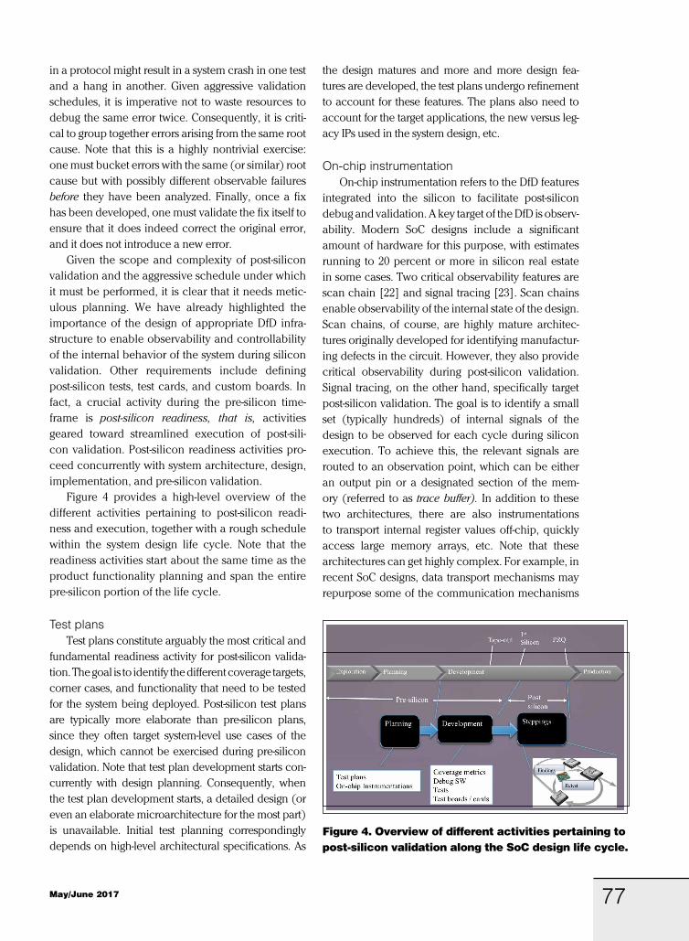
Given the scope and complexity of post-silicon validation and the aggressive schedule under which it must be performed, it is clear that it needs metic-ulous planning. We have already highlighted the importance of the design of appropriate DfD infra-structure to enable observability and controllability of the internal behavior of the system during silicon validation. Other requirements include defining post-silicon tests, test cards, and custom boards. In fact, a crucial activity during the pre-silicon time-frame is post-silicon readiness, that is, activities geared toward streamlined execution of post-sili-con validation. Post-silicon readiness activities pro-ceed concurrently with system architecture, design, implementation, and pre-silicon validation.
Figure 4 provides a high-level overview of the different activities pertaining to post-silicon readi-ness and execution, together with a rough schedule within the system design life cycle. Note that the readiness activities start about the same time as the product functionality planning and span the entire pre-silicon portion of the life cycle.
Test plansTest plans constitute arguably the most critical and
fundamental readiness activity for post-silicon valida-tion. The goal is to identify the different coverage targets, corner cases, and functionality that need to be tested for the system being deployed. Post-silicon test plans are typically more elaborate than pre-silicon plans, since they often target system-level use cases of the design, which cannot be exercised during pre-silicon validation. Note that test plan development starts con-currently with design planning. Consequently, when the test plan development starts, a detailed design (or even an elaborate microarchitecture for the most part) is unavailable. Initial test planning correspondingly depends on high-level architectural specifications. As
the design matures and more and more design fea-tures are developed, the test plans undergo refinement to account for these features. The plans also need to account for the target applications, the new versus leg-acy IPs used in the system design, etc.
On-chip instrumentationOn-chip instrumentation refers to the DfD features
integrated into the silicon to facilitate post-silicon debug and validation. A key target of the DfD is observ-ability. Modern SoC designs include a significant amount of hardware for this purpose, with estimates running to 20 percent or more in silicon real estate in some cases. Two critical observability features are scan chain [22] and signal tracing [23]. Scan chains enable observability of the internal state of the design. Scan chains, of course, are highly mature architec-tures originally developed for identifying manufactur-ing defects in the circuit. However, they also provide critical observability during post-silicon validation. Signal tracing, on the other hand, specifically target post-silicon validation. The goal is to identify a small set (typically hundreds) of internal signals of the design to be observed for each cycle during silicon execution. To achieve this, the relevant signals are routed to an observation point, which can be either an output pin or a designated section of the mem-ory (referred to as trace buffer). In addition to these two architectures, there are also instrumentations to transport internal register values off-chip, quickly access large memory arrays, etc. Note that these architectures can get highly complex. For example, in recent SoC designs, data transport mechanisms may repurpose some of the communication mechanisms
Figure 4. Overview of different activities pertaining to post-silicon validation along the SoC design life cycle.

78 IEEE Design&Test
Tutorial
already present in the system, e.g., universal serial bus (USB) port. This requires a thorough understanding of both the functionality and the validation use cases to ensure that they do not interfere when using the same interface. Finally, there is instrumentation to provide controllability of the execution, e.g., by overriding the system configuration, updating microcode on-the-fly during execution, etc.
There has recently been significant research on improving post-silicon observability through disci-plined DfD architecture. Some of the key work in this area has focused on trace signal selection, and we discuss this problem in the “Trace signal selection” section. Among on-chip instrumentation techniques, one of the earliest work is due to Gopalakrishnan and Chou [24]. They use constraint solving and abstract interpretation to compute state estimates for memory protocols. Park and Mitra [4] develop an architecture called IFRA for disciplined on-chip observability of pipelined microprocessors. Boule et al. [25] present architectures for post-silicon asser-tion checkers. Ray and Hunt [7] present an archi-tecture for on-chip monitor circuits for validation of specific concurrent protocols.
Debug software developmentDebug software is another crucial component of
post-silicon validation readiness. It includes any soft-ware tool and infrastructure that is necessary to ena-ble running post-silicon tests and facilitating debug, triage, or validation of different coverage goals. We can categorize debug software roughly into the fol-lowing classes.
Instrumented system software: Post-silicon valida-tion, particularly for hardware logic and compat-ibility validation, requires running long compli-cated tests, identifying complex corner cases, and root-causing errors excited by subtle hardware/software coordination. To achieve this, one typi-cally needs to run an application software stack on the target system. Doing this by executing an application on top of an off-the-shelf operating sys-tem is typically difficult. Modern operating systems (e.g., Linux, Windows, Android, MacOS, etc.) are highly optimized for performance and power con-sumption, and significantly complex. To enable debug of underlying hardware issues one typically needs a highly customized system software, with a reduced set of “bells and whistles” while including
a number of hooks or instrumentations to facilitate debug, observability, and control. For example, one may want to trace the sequence of branches taken by an application in order to excite a specific hard-ware problem. To achieve this, often specialized operating systems are implemented that are targeted for silicon debug. Such system software may be writ-ten by silicon debug teams from scratch, or by signif-icantly modifying the off-the-shelf implementations.
Tracing, triggers, and configurations: Some cus-tomized software tools are also developed for con-trolling, querying, and configuring the internal state of the silicon. In particular, there are tools to query or configure specific hardware registers, setting triggers for tracing, etc. For example, one may wish to trace a specific signal S only when some internal register R contains a specific value u. Assuming that both S and R are observable, one needs software tools to query R and configure signal tracing to include S when R contains u.
Transport Software: Access software refers to tools that enable transport of data off-chip from silicon. Data can be transferred off-chip either directly through the pins, or by using the available ports from the platform (e.g., USB and PCIe). For example, transporting through the USB port requires instru-mentation of the USB driver to interpret and route the debug data while ensuring the USB functionality is not affected during normal execution. Note that this can become highly complex and subtle, particu-larly in the presence of other features in the SoC such as power management. Power management may in fact power down the USB controller when the USB port is not being used by the functional activity of the system.
The instrumented driver ensures that debug data is still being transported while still facilitating the power-down functionality of the hardware to be exercised during silicon validation.
Analysis software: Finally, there are software tools to perform analysis on the transported data. These include tools to aggregate the raw signal or trace data into high-level data structures (e.g., interpret-ing signal streams from the communication fabric in the SoC as messages or transactions among IPs), comprehending and visualizing hardware/software coordinations, as well as tools to analyze such traced and observed data for further high-level debug

79May/June 2017
(e.g., to estimate congestion across the communica-tion fabric, traffic patterns during internal transactions, and power consumption during system execution).
One critical challenge in developing (and val-idating) debug software is its tight integration with the target hardware design to be validated. Note that typically software development and validation make use of a stable hardware platform, e.g., one devel-ops application software on top of a general-purpose hardware instruction set architecture such as X86 or ARM. However, debug software is developed for an under-development target platform, often with evolving and changing features (e.g., in response to design or architectural challenges discovered late). This makes debug software design a vexing and complex problem in hardware/software co-design and co-validation. Indeed, it is not uncommon in post-silicon validation to root-cause an observed fail-ure to an issue with the debug software rather than the target system. Developing a streamlined technol-ogy for debug software development and validation is a challenging area of research.
Test generation and testing setup designThe central component of silicon debug is the
set of tests to run. For the validation to be effective, the tests must expose potential vulnerabilities of the design, and exercise different corner cases and con-figurations. Post-silicon tests can be divided into the following two categories.
Focused (directed) tests: These are tests carefully crafted by expert test writers to target specific fea-tures of the system (e.g., multiprocessor and chipset protocols, CPU checks for specific register config-urations, address decoding, power management features). Developing such tests involves signifi-cant manual effort. Furthermore, the tests are often extremely long and targeted, running for several hours on silicon.
Random and constrained-random tests: In addition to focused tests, one exercises system features through random and constrained-random testing. Examples of such tests include executing a random sequence of system instructions, exercising concurrent inter-leavings, etc. The goal of these tests is to exercise the system in ways not conceived by humans, e.g., random instruction tests can include hundreds of millions of random seeds generating instruction sequences.
In addition to the tests themselves, their appli-cation requires development of specialized periph-erals, boards, and test cards. This is specifically pertinent for compatibility validation where the system needs to be exercised for a large number of peripheral devices, software versions, and platform features. The “Test generation” section test genera-tion steps in detail.
Toward standardization of validation Infrastructure
As is evident from the above discussions, post-sil-icon readiness is a complex and hard problem. To facilitate this, there have been efforts across the industry to standardize the debug and observabil-ity architectures. Two such standardizations are the ARM Coresight and Intel Platform Analysis Tool. Both these architectures include a set of hardware IPs (e.g., for collecting, synchronizing, and times-tamping signal traces and other observability col-lateral from different design blocks, routing them to output ports and system memory), and software APIs for configuration, triggering, transport, and analysis. The specifics of the architectures vary. Coresight architecture [26] is instantiated into Macrocells that can interact with the IP functionality through a standard interface. Platform Analysis Tool includes a specialized IP called Trace Hub [27] responsible for aggregation and transport of both hardware and software traces, together with APIs that enable direct interaction with this IP for transport and analysis.
While such standardization assists in stream-lining post-silicon readiness development, it must be emphasized that the current state of the art in standardization is rather rudimentary. For instance, the software tools to extract trace data for both the architectures above are typically APIs for accessing different internal design collateral; little assistance is provided to identify the specific collateral that would be useful or profitable for debug purposes. It is left to the expertise of the human designer and val-idator to “hook up” the APIs with the hardware and software content in the target design for achieving validation objectives.
Trace signal selectionIn this section, we delve slightly deeper into one
aspect of post-silicon planning, viz., trace signal selection. As discussed in the “Planning for post- silicon readiness” section, trace signals are used to

80 IEEE Design&Test
Tutorial
address the observability limitation during post-sili-con debug. The basic idea is to trace a set of signals during run time and store in a trace buffer such that the traced values can be used during post-silicon debug. It is important to note that since I/O speed (using JTAG, for example) is significantly slower than the speed of execution (e.g., MHz versus GHz), it is not possible to dump the traced values through I/O ports during execution. Therefore, internal trace buffer is required. Trace signal selection needs to maintain various design constraints. For example, the trace buffer size directly translates to area and power overhead. Moreover, routing the selected signals to the trace buffer may face congestion and other lay-out-related issues. As a result, in a design with millions of signals, a typical trace buffer traces a few hundred signals for a few thousand cycles. For example, a 128 x 2048 trace buffer can store 128 signals over 2048 clock cycles. Design overhead considerations directly impose two constraints— how to select a small num-ber of trace signals that can maximize the observabil-ity, and how to effectively utilize traced values for a small number of cycles to enable meaningful debug.
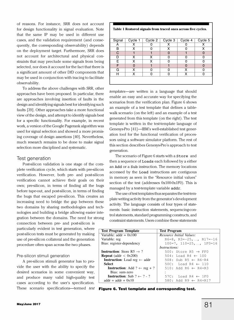
In post-silicon debug, unknown signal states can be reconstructed from the traced states in two ways—forward and backward restoration. For example, if one of the inputs of an and gate is selected as a trace signal and the traced value is ‘0’, we can definitely infer through forward res-toration that the output of that and gate should be ‘0’ in that clock cycle. Similarly, if we know the output of an and gate to be ‘1’ in a specific clock cycle, we can infer using backward restoration that the inputs of that and should be all ‘1’s. Of course, in many scenar-ios, we need to know the values of multiple signals to be able to restore the values of untraced signals.
One metric used frequently to measure quality of selected trace signals is the state restoration ratio (SRR), which is based directly on the idea of reconstructing values of untraced signals from traced ones. To understand SRR, consider the circuit shown in Figure 5. The example cir-cuit has eight flip-flops. Let us assume that the trace buffer width is 2, that is, states of two signals can be traced. The approaches of [29] and [30] will select C and F as trace signals. Table I shows the restoration of other sig-nals using the traced values of C and
F (shaded rows in the table). For example, if we know C is ‘0’ at clock cycle 3, we can infer that both A and B were ‘0’ in the previous cycle (clock cycle 2). Since we know now that A is ‘0’ at clock cycle 2, D should be ‘0’ in the next cycle (clock cycle 3). This process of forward and backward restoration is continued until no new values can be restored. The ‘X’s represent those states that cannot be determined. The SRR is then defined as
RR = # of states restored + # of traced states __________________________ number of traced states
(1)
In this example, we have traced 10 states (two sig-nals for five cycles) and we are able to restore an additional 16 states. Therefore, the restoration ratio is (16 + 10) ÷ 10 = 2.6.
SRR-based signal selection techniques can be broadly divided into three categories. The signal selection techniques in the first category performs structural analysis of the design and selects the ben-eficial signals based on their likelihood in restor-ing the unknown (untraced) signals [28]–[31]. These approaches are very fast but they sacrifice the restorability. On the other hand, the simula-tion-based signal selection techniques [32] utilize the deterministic nature of the signals in identify-ing the most profitable trace signals. This approach provides superior restoration quality but incurs pro-hibitive computation overhead. The third category of techniques tries to combine the advantages of both approaches utilizing hybrid [33], ILP [34], and machine learning [35], [36] techniques. There are also various approaches that try to take advantage of both trace and scan signals to improve post-sili-con observability [37], [38].
We should point out that while SRR is widely used today as a research vehicle in evaluating trace signal quality, we are not aware of any industrial report on application of SRR. This is due to a variety
Figure 5. An example circuit with 8 flip-flops [28].
81May/June 2017
of reasons. For instance, SRR does not account for design functionality in signal evaluation. Note that the same IP may be used in different use cases, and the validation requirement (and conse-quently, the corresponding observability) depends on the deployment target. Furthermore, SRR does not account for architectural and physical con-straints that may preclude some signals from being selected, nor does it account for the fact that there is a significant amount of other DfD components that may be used in conjunction with tracing to facilitate observability.
To address the above challenges with SRR, other approaches have been proposed. In particular, there are approaches involving insertion of faults in the design and identifying signals best for identifying such faults [39]. Other approaches take a more functional view of the design, and attempt to identify signals best for a specific functionality. For example, in recent work, a version of the Google Pagerank algorithm was used for signal selection and showed a more promis-ing coverage of design assertions [40]. Nevertheless, much research remains to be done to make signal selection more disciplined and systematic.
Test generationPost-silicon validation is one stage of the com-
plete verification cycle, which starts with pre-silicon verification. However, both pre- and post-silicon verification cannot achieve their goals on their own; pre-silicon, in terms of finding all the bugs before tape-out, and post-silicon, in terms of finding the bugs that escaped pre-silicon. This creates an increasing need to bridge the gap between these two domains by sharing methodologies and tech-nologies and building a bridge allowing easier inte-gration between the domains. The need for strong connection between pre- and post-silicon is particularly evident in test generation, where post-silicon tests must be generated by making use of pre-silicon collateral and the generation procedure often span across the two phases.
Pre-silicon stimuli generationA pre-silicon stimuli generator has to pro-
vide the user with the ability to specify the desired scenarios in some convenient way, and produce many valid high-quality test cases according to the user’s specification. These scenario specifications—termed test
templates—are written in a language that should enable an easy and accurate way for specifying the scenarios from the verification plan. Figure 6 shows an example of a test template that defines a table-walk scenario (on the left) and an example of a test generated from this template (on the right). The test template is written in the test-template language of Genesys-Pro [41]—IBM’s well-established test gener-ation tool for the functional verification of proces-sors using a software simulator platform. The rest of this section describes Genesys-Pro’s approach to test generation.
The scenario of Figure 6 starts with a Store and then a sequence of Loads each followed by a either an Add or a Sub instruction. The memory locations accessed by the Load instructions are contiguous in memory as seen in the “Resource initial values” section of the test (addresses 0x100-0x1F0). This is managed by a test-template variable addr.
The use of test templates thus separates the test-tem-plate writing activity from the generator’s development activity. The language consists of four types of state-ments: basic instruction statements, sequencing-con-trol statements, standard programming constructs, and constraint statements. Users combine these statements
Table 1 Restored signals from traced ones across five cycles.
Figure 6. Test template and corresponding test.

82 IEEE Design&Test
Tutorial
to compose complex test templates that capture the essence of the targeted scenar-ios, leaving out unnecessary details. This allows directing the generator to a specific area, be it a small or a large one.
The generated test cases must be valid according to the processor’s architecture, and satisfy the user’s request specified in the template. In addition, they should also be different from each other as much as possible. This is done by specifying the rules determining the validity of a test case, as well as the user requests as con-straints. The generator, then, produces a test case by random sampling of the solu-tion space to the resulting constraints sat-isfaction problem [42].
The distribution of the generated tests should not be uniform, as verification engineers would like to favor tests that include interesting verification events (e.g., register dependency, memory colli-sions), especially ones that are extremely unlikely to occur under uniform distribution. This is done by having knowledge embedded in the generator, allow-ing it to bias random decisions toward stimuli that causes interesting events [42]. This testing knowledge defines the interesting verification events, including the stimuli that trigger them. As the stimuli for some interesting events depend on the processor’s state, the generator also employs a reference model of the DUV, simulating on it for every generated instruction. This way the generator maintains an accurate view of all the architectural resources, taking it into account during generation of interesting events. This scheme is shown in the lower part of Figure 7.
Genesys-Pro has been in use by IBM for over 15 years. It has proven to be effective in meeting the users’ requirements, enabling them to write test tem-plates implementing the core verification plans of IBM’s complex processors [43].
A unified verification methodologyTo better integrate post-silicon validation to
the overall verification process and improve its synergy with pre-silicon verification, a unified ver-ification methodology is needed that is fed from the same verification plan source. A key ingredient for the success of such methodology is providing common languages for the pre- and post-silicon aspects of it in terms of test specification, progress
measure, etc. Figure 8 depicts such a methodology. This verification methodology leverages three differ-ent platforms: simulation, acceleration, and silicon. The methodology requires three major components: a verification plan, directable stimuli generators suited to each platform, and functional coverage models. Note that important aspects in any verification meth-odology, such as checking, are omitted from the figure to maintain focus on stimuli generation.
The verification plan includes a long list of line items, each targeting a feature in the DUV that needs to be verified. Each such feature is associ-ated with coverage events that the verification team expects to observe during the verification process and the methods to be used to verify the feature. The verification plan is implemented using random stimuli generators that produce a large number of test cases, and coverage tools that look for the occurrence of events in the verification plan. The random stimuli generators are directed toward the verification goals by using test templates. The test templates allow the generators to focus on areas in the DUV ranging from large generic areas, like
Figure 7. Threadmill versus Genesys-Pro tool flows.
Figure 8. A unified verification methodology.

83May/June 2017
the floating-point unit, to very specific areas, like a bypass between stages of the pipeline. Coverage analysis identifies gaps in the implementation of the plan. Its feedback is used to modify test templates that do not fulfill their goals, and create new ones.
This methodology is extended to post-silicon validation by leveraging the acceleration platform to measure coverage of post-silicon tools. To take advantage of the coverage information collected by the accelerators and use it in the post-silicon, shortly before first silicon samples come back from the fab, a regression suite of exerciser test templates is cre-ated based on the coverage achieved on the accel-erators. This regression suite is then used to continue the verification process on the silicon platform.
With the unified methodology, each of the line items in the verification plan is attached to one or more target platforms on which it will be verified. These line items are converted to test templates in the languages of the generation tools used by each platform. A key ingredient for the success of the unified methodology is similar operation of the stimuli generators. In this sense, designers would like the generators to use the same test-template language, and when provided with the same test template, one would like the tools to produce simi-lar (though not identical) test cases. Of course, the different platforms provide different opportunities and put different constraints and requirements on the generation tools, but whenever possible, there are advantages to having similar tools. First, the pre- and post-silicon teams can share the task of under-standing the line-items in the verification plan and planning ways to test them. In addition, the com-mon language allows for easier adaptation of test templates from one platform to another. For exam-ple, when a bug is detected on the silicon platform, narrowing down the test template and hitting it on the simulation platform eases the root-cause analy-sis effort.
It is important to note that the differences between platforms also dictate differences in the way test templates are written for pre- and post-sil-icon tools. A test template could be very specific and describe a small set of targeted tests or it could be more general leaving more room for randomiza-tion. The validation engineer writing test templates for a post-silicon exerciser must bear in mind the fact that the test template is used to generate a huge number of test cases and get many processor cycles.
To effectively use these test cycles, the test template must allow for enough interesting variation. A test template that is too specific will quickly “run out of steam” on silicon and start repeating similar tests. A pre-silicon test template on the other hand would typically be more directed to ensure that the tar-geted scenarios are reached within the fewer cycles available on simulation. There are also many efforts in automated generation of directed tests using for-mal methods [44]–[48].
ThreadmillThreadmill was developed in IBM for the purpose
of enabling the unified methodology described in the previous subsection; namely, to support a verifi-cation process guided by a verification plan by ena-bling the validation engineers to guide the exerciser through test templates. The high-level tool architec-ture of Threadmill is depicted in Figure 7, along with the flow of Genesys-Pro [49]—the pre-silicon test generator tool described in the “Pre-silicon stimuli generation” section.
Like Genesys-Pro, the main input to Threadmill is a test template that specifies the desired scenarios. As described earlier, the templates used for pre- and post-silicon tests have different characteristics. The test-template language of Threadmill is very similar to the language of Genesys-Pro, but to adhere to the simplicity and generation of speed requirements, several constructs that require long generation time, such as events, are not included in Threadmill’s lan-guage. Other inputs to Threadmill are the architec-tural model and testing knowledge and the system topology. Again, for simplicity reasons, many testing knowledge items that are included in Genesys-Pro models are not used by Threadmill.
The Threadmill execution process starts with a builder application that runs offline to create an executable exerciser image. The role of the builder is to convert the data incorporated in the test template and the architectural model into data structures that are then embedded into the exerciser image. This scheme eliminates the need to access files or data-bases while the exerciser is running.
The exerciser image is composed of three major components: a thin, OS-like, layer of basic services required for Threadmill’s bare-metal execution; a representation of the test template, architectural model, and system configuration description as simple data structures; and fixed (test-template

84 IEEE Design&Test
Tutorial
independent) code that is responsible for exercis-ing. The executable image created by the builder is then loaded onto the silicon platform where the exerciser indefinitely repeats the process of gener-ating a random test case based on the test template, the configuration and the architectural model, exe-cuting it, and checking its results.
In the case of Genesys-Pro, the test generation process is carried outside of the simulation envi-ronment (say on a dedicated server) and only the generated tests are loaded and run on the simulation platform. Simulation cycles would be too slow to allow generation on simulation. The “offline” gener-ation on the other hand can afford to spend time on sophisticated generation and checking—for exam-ple by using a reference-model as shown in Figure 7 for Genesys-Pro. Threadmill’s test generation compo-nent was designed to be simple and fast. Therefore, IBM designers opted for a static test generator that does not make use of a reference model. Reference models provide the generator information about the state of the processor before and after the genera-tion of each instruction. This information is used for checking but also to create more interesting events. Reloading resources, such as registers, can be a par-tial replacement to the reference model, but this solution potentially interferes with the generation of the requested scenarios. For data-oriented events, such as divide-by-zero, a simple yet effective solution is to reserve registers to hold interesting values. Of course, the generator has to ensure that the reserved registers are not modified during the test.
Execution of the same test case multiple times is used as a partial replacement for checking done by the reference model. This is done by comparison of certain resource values such as registers and part of the memory for consistency in different executions of the test case. Running the same test case multiple times may result in different results even when bugs are not present. For example, when several threads write to the same memory location, the final value at this location depends on the order of the write oper-ations. This requires that certain mechanisms be implemented in the generator to restrict the number of unpredictable resources. Although the multipass comparison checking technique is limited, it has proven to be effective when control-path oriented bugs, or bugs that reside in the intersection of the control and data paths, are concerned. To increase the probability of exposing such bugs, it is beneficial
to introduce some kind of variability into the differ-ent execution passes, while making sure that the var-iability maintains the predictability of the compared resources. This can be done, for example, by chang-ing the machine mode, or changing thread priorities.
Tests targeting errorsWe now turn to the question: how can we ensure
that a test excites a bug and propagates it to a failure within a reasonable time? In this subsection, we con-sider the question from the perspective of test gener-ation; in the next subsection the same question will be considered from the perspective of observability constraints.
Traditionally, post-silicon tests have sported a long latency between when a bug is excited and when its effect is observed as a failure. For instance, consider a memory write to some address that writes an incor-rect value. The effect of this bug may not be observed unless the value written is subsequently read (maybe several thousands of cycles later) and the error result-ing from this read propagated to cause some observ-able effects. Clearly, it is important to reduce the latency of error observability, from the point in which the bug is triggered to an observable effect.
There has been significant research in develop-ing effective post-silicon tests. In particular, a general technique called quick error detection (QED) spe-cifically focuses on reducing the latency mentioned above [50], [51]. The idea is to transform a test into another one with lower latency between bug excita-tion and failure. For instance, for the memory read example above, a QED test would transform the orig-inal test by introducing a memory read immediately after each memory write; thus, an error introduced by the write would be excited immediately by the corresponding read. Note that doing this in general requires a comprehensive characterization of errors in terms of a cause–effect relationship. QED manages it by defining this relationship for errors in a num-ber of categories. By capturing a diversity of error characterizations, it has managed to be successfully adapted for a diversity of post-silicon tests, including those for functional as well as electrical errors.
Observability-aware test generationObservability constraints make it difficult to diag-
nose bugs. In fact, it is also difficult to figure out if a test has executed as expected, if the result of that test execution activates a signal that is not observable.

85May/June 2017
Therefore, it is crucial that the post-silicon tests are observable directly (if it activates one of the trace sig-nals) or indirectly (values of the activated signal can be restored using the trace signals). Unfortunately, it would be hard to generate observability-aware tests for various reasons. First, the post-silicon test genera-tion and trace signal selection are typically performed concurrently by different teams during an industrial SoC development. Moreover, it is difficult to per-form automated generation of observability-aware directed tests after the observability architecture has been defined. This is due to the fact that such a test generation approach would require analysis of com-plex and potentially buggy RTL models. Industrial RTL models consist of millions of lines of code, and therefore, automated formal analysis of such mod-els exceeds the capacity limitations of directed test generation tools. Even if such an analysis was possi-ble, the generated test would not be useful if the RTL models contains functional or design errors—an erro-neous model can at best lead to generation of buggy tests, which is unlikely to activate the design flaws. Even if it activates a specific scenario, the accuracy of such a validation method becomes questionable.
Recent research efforts [52] provide an alternative mechanism to generate observability-aware post-sil-icon tests using golden pre-silicon models. The test generation is performed by analyzing golden transaction-level models (TLM) instead of buggy RTL models. Analysis of TLM model also takes care of the scalability issue since a TLM model is significantly simpler than the respective RTL model. Clearly, this approach requires a golden TLM model. This work also assumes that both TLM and RTL models have the same input/output interfaces at both SoC and individual component levels. This is rea-sonable for SoC design since it consists of hardware or software intellectual property (IP) blocks with well-defined interfaces.
Figure 9 provides an overview of observ-ability-aware test generation for a given RTL assertion. This approach involves four important steps:
1) defining test targets with observability constraints;
2) mapping test targets from RTL to TLM; 3) test generation using TLM model; 4) translating TLM tests to RTL tests.
This work essentially incorporates observability constraints into an RTL assertion to create a new RTL assertion. The modified assertion is then mapped to a TLM property. The TLM property is used to auto-matically construct a TLM test. The last step is to con-vert the generated TLM test to an RTL test [53]. The generated RTL test is observability-friendly, since it would not only activate the assertion but also propa-gate its effects to the observability architecture (e.g., trace signals).
Post-silicon validation of IBM POWER8In this section, we provide a high-level overview
of the post-silicon methodology and technologies put into use for functional validation of POWER8. We describe various factors that contributed to this successful bring-up. A detailed discussion on the functional verification of POWER8 and its bring-up can be found in [54] and [55].
The POWER8 ChipPOWER8 is the latest IBM chip in the POWER
series. Designed for high-end enterprise-class serv-ers, it is one of the most complex processors ever created. The POWER8 chip is fabricated with IBM’s 22 nm silicon-on-insulator technology using copper
Figure 9. Observability-aware test generation consists of four important steps: construct RTL assertion with observability constraints, map RTL assertion to TLM, generate TLM test, and translate TLM to RTL test.

86 IEEE Design&Test
Tutorial
interconnects and 15 layers of metal. The chip is 650 mm2 and contains over 5 billion transistors.
Figure 10 depicts a high-level block diagram of the POWER8 processor chip. Each processor chip has 12 cores. Each core is capable of 8-way simul-taneous-multithreading (SMT) operation, and can issue up to 10 instructions every cycle. The memory hierarchy includes a per-core L1 cache, a per-core SRAM-based 512KB L2 cache, and an eDRAM-based shared L3 cache. In addition, an off-chip eDRAM L4 cache per memory buffer chip is supported. There are two memory controllers on the chip supporting a sustained bandwidth of up to 230 GB/s. The chip also holds a set of hardware accelerators, including a cryptographic accelera-tor and a memory compress/decompress mech-anism. Finally, the chip includes a PCIe adapter and bridge to a bus supporting a coherent con-nection to an FPGA. The FPGA is directly acces-sible to user applications through a hashed table translation.
Preparing for the labThe bring-up work of POWER8 started way before
silicon samples were ready. The team responsible for preparing the tools and tests for the lab began its work as soon as the key features of POWER8 were determined at the high-level design (HLD) stage. The first step in that work was to ensure that the post-sil-icon tool teams better understand the new features they need to support and the design team under-stand the validation requirements and incorporate them into the design.
When sufficient functional stability was achieved, the pre-silicon verification team, together with the exerciser team, started running exerciser shifts on Awan simulation acceleration platform [56]. This phase, termed exercisers on accelerator (EoA), achieved several goals. First, it ensured the quality of the exercisers software. In addition, it helped the pre-silicon verification of POWER8. In fact, EoA was responsible for finding about 1 percent of the total bugs found in pre-silicon verification. Finally, EoA was used to develop and test the shifts that were later used during the actual bring-up.
To that extent, an important aspect of the EoA work was the synthesis of coverage monitors syn-thesized into the DUT model. These coverage mon-itors were added to the logic model running on the accelerator, but not to the silicon itself, because of
area, timing, and power issues. Leveraging acceler-ation-synthesized coverage monitors allowed the use of a pre-silicon-like coverage-driven method-ology for post-silicon test development [57]. With this approach, the exerciser shift developers could validate that a specific shift covers the targeted func-tionality. This is done by observing that the related coverage events are hit when the exerciser shift is run on the accelerator. The acceleration-synthesized coverage monitors played a major role in selecting which shifts to run during bring-up to best utilize the scarce silicon resources. There are also recent efforts in post-silicon coverage analysis without using syn-thesized coverage monitors [58]. A different use of accelerators during the bring-up preparation was to prepare the different procedures and tools for the lab team. This included the validation of the differ-ent steps required to boot the system (virtual pow-er-on, or VPO), track the execution of an exerciser as it runs, and dump and format debug data from the embedded trace arrays.
Triggering bus—Stimuli generationBare-metal exercisers (an example of which is
described in the “Threadmill” section) were the pri-mary vehicle for test-case generation in the POWER8 post-silicon validation. The characteristics of the post-silicon platforms create challenges and impose tradeoffs that affect the design of these exercisers. While post-silicon platforms offer a huge number of execution cycles, their low availability and high cost calls for maximizing the time spent executing test cases and minimizing overhead. Accordingly, the exerciser team developed a set of exercisers, each
Figure 10. The POWER8 processor chip.

87May/June 2017
capturing a different tradeoff between generation complexity and checking capabilities. Bare-metal exercisers possess a list of attributes that make them highly suitable for post-silicon validation. Bare-metal exercisers are inherently “self-contained,” meaning that once the exerciser shift is loaded onto the plat-form, be it an accelerator or a silicon one, it can run “forever” with no interaction with the environment. This significantly reduces the overhead related to initializing the platform, loading the exerciser, and so on.
Overall, during the POWER8 pre-and post-sili-con development process, the bare-metal exercisers approach proved highly successful, as in the case of other previous processors. This approach is key in IBM’s post-silicon validation strategy. In fact, bugs that were found with OS-based tests or actual software are considered escapes from our validation strategy.
In addition to bare-metal exercisers, IBM design-ers leveraged a set of hardware irritators embedded in the design. A hardware irritator is a piece of logic embedded in the design that can trigger microarchi-tectural events at random. The irritators are initial-ized during the processor’s power-on sequence, and randomly inject events as the processor executes instructions. For example, an irritator can be used to flush the pipeline at random, without having the executed instruction stream create the conditions required for this event.
Irritators are extremely useful in bringing the DUT to some “tough” corners, without creating the stimuli needed to actually reach these corners. Furthermore, irritators can mimic large system behavior. For example, in a single chip system, an irritator can inject a random translation lookaside buffer (TLB) invalidate-entry event as if it were com-ing from a different chip.
Different components in the POWER8 chip sup-port nonfunctional running modes, introduced for the sake of validation. These modes further assisted the bring-up team in stressing the design. For exam-ple, the POWER8 L2 cache supports a mode in which almost every access would trigger a cast-out. By set-ting the processor to this state, one could aggravate the stress on the L3 cache.
Since hardware irritators and nonfunctional modes are embedded in the design, and, accord-ingly, have an overhead in terms of area and power, they must be carefully thought of and designed as a part of the processor.
CheckingPOWER8 employed two main checking tech-
niques in its post-silicon validation: checkers embed-ded in the hardware and software checkers that are part of the bare-metal exercisers. Hardware-based checkers were designed and embedded into the POWER8 processor. These checkers cover some generic erroneous behavior such as access out of memory, and a timer- based hang checkers for instruction completion.
During the POWER8 post-silicon validation, it was easier to debug failures triggered by hardware-based checkers. This was because when a failure was triggered by such a checker, the DUT was stopped fairly close to the origin of the bug. Accordingly, the debug logic, once configured to trace the relevant component in the design, typically contained valu-able hints as to the origin of the bug. Furthermore, some checkers provide an initial indication when they fire. For example, when the access out of mem-ory checker fires, the transaction that triggered it is captured in the bus’ debug logic and points to the hardware thread and address that triggered the fail.
Despite their effectiveness, the use of hard-ware-based checkers is limited due to their high cost in terms of area and power, and their effect on tim-ing. Therefore, software-based checkers were also heavily used for failure detection in the POWER8 post-silicon validation.
Bare-metal exercisers employ a checking tech-nique called multipass consistency checking [59]. In this technique, every test case is executed sev-eral times (passes). The first pass is referred to as a reference pass, and the values of certain resources, such as architected registers and some memory, are saved at the end of the execution of this pass. After following passes, the exerciser compares the end-of-pass values with those of the reference pass. In case an inconsistency is detected, the error is reported and the execution is stopped. The multipass con-sistency checking technique imposes restrictions on test generation. For example, write–write collisions between different threads to the same memory loca-tion, where the order of thread accesses cannot be determined may yield inconsistent results and are therefore not supported.
Multipass consistency failures were very hard to debug. This occurred primarily because the check-ing flags the error millions, and sometimes billions, of cycles after the error first occurred.
88 IEEE Design&Test
Tutorial
Despite the restrictions and the difficulty in debugging such failures, multipass consistency checking has proven useful in finding some of the toughest functional bugs in POWER8.
In addition to multipass consistency checking, exerciser developers introduced self-checking state-ments into some of the scenarios. Such checks were only applicable in directed scenarios and required manual labor, but were useful in better localizing the fail, preventing errors from being masked, and extending the attributes checked for such scenarios.
DebugAs discussed in the “Silicon validation challenges”
section, post-silicon debug is a major challenge. Even with the best practices used in the IBM post-sili-con lab during the validation of the POWER8 proces-sor, debugging of failures found in the lab was a long and tedious process.
When a test case failed in the lab, the first step in its debug is to determine the cause of the failure. The origin of the failure could be one of numerous reasons, including a manufacturing issue, erroneous machine setup, an electrical bug, a functional bug, or a software bug in the exerciser. This is done by rerunning the failing tests in similar but not identical settings. For example, manufacturing problems can be detected by repeating the same test on a differ-ent core or chip and watch the test passing. Next, additional experiments were conducted with a goal to determine key aspects in the hardware configu-ration that were required to hit the failure. Such experiments can be done by changing the hardware setup, e.g., disabling some of the processor cores, or modifying the number of active hardware threads in the core.
Another approach to debugging failures was to reproduce them on the acceleration platform. This approach relied heavily on the use of tools, specifi-cally, bare-metal exercisers, that can effectively run on both the hardware and an accelerator. Because the hardware platform is over six orders of magni-tude faster than the acceleration platform, a failing shift could not be migrated from silicon to accelera-tion as-is. Typically, a set of experiments is required to fine-tune the exerciser shift in order to make it hit the failure on silicon fast enough to enable rec-reation on acceleration. With the enhanced observ-ability capabilities of the acceleration platform, recreating a bug was sufficient in order to provide
the logic designer all the data required to determine the root cause of the bug.
Finally, if neither of the approaches described above succeeded, the lab team had to drive the debug process based only on the data available from the on-chip trace arrays. The POWER8 debug logic, which is similar to that described by Riley et al. [60], has three key attributes that enable effective debug. First, the trace array can be configured, as a part of the hardware’s initialization, to track different parts of the design. Second, the debug logic can be config-ured to trace compound events. Finally, the events on which the trace arrays store their input can also be configured. Therefore, instead of saving inputs at every clock cycle, the trace arrays can be configured to latch data only when some event is detected. This enabled noncontinuous tracing of events, which has proven useful in some hard debug cases. As pre-sented in the “Trace signal selection” section, select-ing which signals can be traced is an important part of the work done as part of the preparation to the bring-up. Selecting which signals to actually trace and when to trigger tracing is a challenge the lab team needs to handle.
To that extent, a key feature facilitating effective post-silicon debug in POWER8 is the existence of the cycle reproducible environment. This environ-ment is a special hardware mode in which execut-ing the same exerciser shift would reproduce the exact same results. Leveraging this mode, the team could rerun the same exerciser shift repeatedly with different trace array configurations in different runs, e.g., by terminating the trace at different cycle count [60]. This option, combined with BackSpace [8], was used to aggregate data from multiple runs for longer traces that significantly improved the ability for efficient debug.
ResultsThe POWER8 bring-up is considered as a very
successful one. The team was able to keep a bug discovery and resolution rate equal to or better than previous POWER processor bring-up efforts, with sig-nificantly less resources.
The results of the POWER8 bring-up are partly depicted by Figure 11 and Table II. Every point in the figure accounts for one bug. The location of the point on the x-axis, termed detect time, relates to the number of days from the beginning of bring-up to the day the bug was first hit. A point’s location on

89May/June 2017
the y-axis, termed debug time, relates to the number of days from the time the bug was first hit to the time its root cause was determined. Table 2 summarizes the data presented in Figure 11. The table shows, per bug severity, the average and 90 percentile of debug time. For example, medium severity bugs required, on average, 10.07 days to root cause, and 90% of all medium severity bugs required 20, or less, days to root cause. Overall, about 1% of all POWER8 bugs were found in the post-silicon validation phase.
The bugs are divided into three classes, based on their severity. The severity of the bug was deter-mined based on a combination of the impact of the bug on the functional behavior of the system, the performance cost of working around the bug (if that was possible), and the complexity of the fix. The severity of a bug could only be determined after its root cause was found and a fix was suggested. Figure 11 shows that the debug time for high severity bugs is significantly lower, on average, than that of other classes of bugs. This indicates that the lab team effectively speculated the severity of each bug at a
very early stage. This is attributed to the expertise of the lab team members; based on the limited data available, they were able to infer the real nature of the bug and its expected severity when the bug was first detected.
Figure 11 also shows how the rigorous prepara-tions for the bring-up paid off. Half of all POWER8 post-silicon bugs were found in the first three months of the bring-up. This is considered a very good result, since during the first two months of the bring-up the team had to dedicate a lot of time to overcoming hardware stability issues and to “screen” the manu-factured chips for good functioning ones.
We have provided an overview of post-silicon validation and debug for heterogeneous SoCs. We have described various challenges in performing post-silicon validation. We also surveyed exist-ing approaches to address these challenges. The importance of post-silicon validation has increased steadily over the years—many studies suggest up to 50% overall cost (time) for post-silicon validation. Considering the dramatic increase in the num-ber of IoT devices in a wide variety of domains, post-silicon validation of SoC designs is expected to remain in the limelight for a long time. Although this paper covered a wide variety of topics related to post-silicon validation and debug, the materi-als discussed here form only the tip of the iceberg of this large and exciting domain. Nevertheless, we hope this paper provides a starting point for researchers in understanding the industrial prac-tice and research challenges in this area. There is a significant scope for pushing the research envelope above and beyond the current limits, and it is crucial that we do so to enable develop-ment of cost-effective, reliable, and secure com-puting systems.
AcknowledgmentsThis work was supported in part by the NSF
Grants (CCF-1218629 and CNS-1441667) and in part by the SRC Grant (2014-TS-2554). Any opinions, find-ings, conclusions, or recommendations presented in this article are only those of the authors, and do not necessarily reflect the views of the National Science Foundation or Semiconductor Research Corporation.
Table 2 Statistics of days to root cause.
Average 90%Low 9.92 22
Medium 10.07 20High 5.96 12
Figure 11. POWER8 bring-up results.

90 IEEE Design&Test
Tutorial
References [1] S. Ray, Y. Jin, and A. Raychowdhury, “The changing
computing paradigm with internet of things: A tutorial
introduction,” IEEE Design Test Comput., vol. 33, no.
2, pp. 76–96, 2016.
[2] D. Evans, “The internet of things—How the next evolution
of the internet is changing everything,” White Paper
Cisco Internet Business Solutions Group (IBSG), 2011.
[3] P. Mishra and N. Dutt, Functional Verification of
Programmable Embedded Architectures: A Top-Down
Approach, Springer-Verlag, 2005.
[4] S.-B. Park, T. Hong, and S. Mitra, “Post-silicon bug
localization in processors using instruction footprint
recording and analysis (ifra),” IEEE Trans. Comput.-
Aided Design Integr. Circuits Syst., vol. 28, no. 10,
pp. 1545–1558, 2009.
[5] V.V. Ethiraj and K. Safford, “PSMI using at-speed scan
capture,” 2011, U.S. Patent App. PCT/US2011/066-656.
[6] R. Rodrigues and S. Kundu, “Shadow checker: A low-
cost hardware scheme for online detection of faults in
small memory structures of a microprocessor,” in Proc.
Int. Test Conf., 2010.
[7] S. Ray and W.A. Hunt, Jr., “Connecting pre-silicon and
post-silicon verification,” in Proc. 9th Int. Conf. Formal
Methods Comput.-Aided Design (FMCAD 2009),
pp. 160–163.
[8] F. M. De Paula, A.J. Hu, and A. Nahir, “nuTAB-
BackSpace: Rewriting to normalize non-determinism
in post-silicon debug traces,” in Proc. Int. Conf.
Comput.-Aided Verifi., 2012, pp. 513–531.
[9] Virutech Simics. [Online]. Available: http://www.simics.
net, 2009.
[10] “Prototyping with virtualizer,” http://www.synop-sys.com/
Prototyping/VirtualPrototyping/Pages/virtualizer.aspx.
[11] Zebu http://www.synopsys.com/tools/verification/
hardware-verification/emulation/Pages/default.aspx.
[12] Palladium Z1 Enterprise Emulation System. [Online].
Available: www.cadence.com.
[13] Veloce2 Emulator. [Online]. Available: https://www.
mentor.com- /products/fv/emulation-systems/veloce.
[14] R. Rowlette and T. Elies, “Critical timing analysis
in microprocessors using near-IR laser-assisted
device alteration (LADA),” in Proc. Int. Test Conf.,
2003, pp. 264–273.
[15] S. Ram et al., “Clock generation and distribution for
the first IA-64 microprocessor,” IEEE J. Solid-State
Circuits, vol. 35, pp. 1545–1552, 2000.
[16] D. Kaiss and J. Kalechstain, “Post-silicon Timing
diagnosis made simple using formal technology,” in
Proc. FMCAD, 2014, pp. 131–138.
[17] O. Olivo et al., “A unified formal framework for
analyzing functional and speed-path properties,” in
Proc. 2011 12th Int. Workshop Microprocessor Test
Verification, 2011, pp. 44–45.
[18] X. Guo et al., “Pre-silicon security verification and
validation: A formal perspective,” in Proc. Design
Autom. Conf., 2015.
[19] Homebrew Development Wiki, JTAG-Hack. [Online].
Available: http://dev360.wikia.com/wiki/JTAG-Hack.
[20] L. Greenemeier, “iPhone hacks annoy AT&T but are
unlikely to bruise apple,” Scientific American, 2007.
[21] E. Seligman, T. Schubert, and M.V.A. Kiran Kumar,
Formal Verification: An Essential Toolkit for Modern
VLSI Design, Morgan Kaufman, 2015.
[22] M. Abramovici et al., “A reconfigurable design-for-
debug infrastructure for SoCs,” in Proc. 43rd Design
Autom. Conf. (DAC 2006), 2006, pp. 7–12.
[23] P. Patra, “On the cusp of a validation wall,” IEEE
Design Test Comp., vol. 24, no. 2, pp. 193–196, 2007.
[24] G. Gopalakrishnan and C. Chou, “The post-silicon
verification problem: Designing limited observability
checkers for shared memory processors,” in Proc. 5th
Int. Workshop Designing Correct Circuits (DCC 2004).
[25] M. Boule, J. Chenard, and Z. Zilic, “Adding debug
enhancements to assertion checkers for hardware
emulation and silicon debug,” in Proc. Int. Conf. Comput.
Design, 2006, pp. 294–299.
[26] CoreSight On-Chip Trace & Debug Architecture.
[Online]. Available: www.arm.com.
[27] Intel® Platform Analysis Library. [Online]. Available:
https://software.intel.com/en- us/intel-platform-
analysis-library.
[28] K. Basu and P. Mishra, “Restoration-aware trace signal
selection for post silicon validation,” IEEE Trans. Very
Large Scale Integr. (VLSI) Syst., vol. 21, no. 4,
pp. 605–613, 2013.
[29] H. F. Ko and N. Nicolici, “Algorithms for state restoration
and trace-signal selection for data acquisition in silicon
debug,” IEEE Trans. Comput.-Aided Design Integr.
Circuits Syst., vol. 28, no. 2, pp. 285–297, 2009.
[30] X. Liu and Q. Xu, “Trace signal selection for visibility
enhancement in post-silicon validation,” in Proc.
Design Auto. Test Eur., 2009.
[31] S. Prabhakar and M. Hsiao, “Using non-trivial logic
implications for trace buffer-based silicon debug,” in
Proc. Asian Test Symp. (ATS), 2009, pp. 131–136.
[32] D. Chatterjee, C. McCarter, and V. Bertacco,
“Simulation-based signal selection for state restoration
in silicon debug,” in Proc. Int. Conf. Comput.-Aided
Design (ICCAD), 2011, pp. 595–601.

91May/June 2017
[33] M. Li and A. Davoodi, “A hybrid approach for fast and
accurate trace signal selection for post-silicon debug,”
in Proc. Design Autom. Test Eur. (DATE), 2013,
pp. 485–490.
[34] K. Rahmani, P. Mishra, and S. Ray, “Efficient trace
signal selection using augmentation and ILP
techniques,” in Proc. Int. Symp. Quality Electron.
Design (ISQED), 2014, pp. 148–155.
[35] “Scalable trace signal selection using machine
learning,” in Proc. IEEE Int. Conf. Comput. Design
(ICCD), 2013, pp. 384–389.
[36] K. Rahmani, S. Ray, and P. Mishra, “Post-silicon trace
signal selection using machine learning techniques,”
IEEE Trans. Very Large Scale Integr. (VLSI) Syst., 2017.
[37] K. Basu, P. Mishra, and P. Patra, “Efficient combination
of trace and scan signals for post silicon validation and
debug,” in Proc. Int. Test Conf. (ITC), 2001.
[38] K. Rahmani, S. Proch, and P. Mishra, “Efficient
selection of trace and scan signals for post-silicon
debug,” IEEE Trans. Very Large Scale Integr. (VLSI)
Syst. vol. 24, no. 1, pp. 313–323, 2016.
[39] J. Yang and N. Touba, “Automated selection of signals
to observe for efficient silicon debug,” in Proc. VLSI
Test Symp., 2009, pp. 79–84.
[40] S. Ma et al., “Can’t see the forest for trees: State
restoration’s limitations in post-silicon trace signal
selcection,” in Proc. ICCAD, 2015, pp. 1–8.
[41] A. Adir et al., “Genesys-pro: Innovations in test
program generation for functional processor
verification,” IEEE Design Test Comput., vol. 21, no. 2,
pp. 84–93, 2004.
[42] Y. Naveh et al., “Constraint-based random stimuli
generation for hardware verification,” AAAI, 2006.
[43] D.W. Victor et al., “Functional verification of
the POWER5 microprocessor and POWER5
multiprocessor systems,” IBM J. Res. Develop.,
vol. 49, no. 4, pp. 541–554, 2005.
[44] M. Chen et al., System-Level Validation: High-Level
Modeling and Directed Test Generation Techniques,
Springer-Verlag, 2012.
[45] X. Qin and P. Mishra, “Directed test generation for
validation of multicore architectures,” ACM Trans.
Design Autom. Electron. Syst. (TODAES), 2012.
[46] M. Chen and P. Mishra, “Property learning techniques
for efficient generation of directed tests,” IEEE Trans.
Comput. vol. 60, no. 6, pp. 852–864, 2011.
[47] “Functional test generation using efficient property
clustering and learning techniques,” IEEE Trans.
Comput.-Aided Design Integr. Circuits Syst., vol. 29,
no. 3, pp. 396–404, 2010.
[48] F. Farahmandi and P. Mishra, “Automated test
generation for debugging arithmetic circuits,” in Proc.
Design Autom. Test Eur. (DATE), 2016.
[49] M.L. Behm et al., “Industrial experience with test
generation languages for processor verification,” in
Proc. DAC, 2004, pp. 36–40.
[50] T. Hong et al., “QED: Quick error detection tests for
effective post-silicon validation,” in Proc. Int. Test
Conf., 2010, pp. 154–163.
[51] D. Lin et al., “Effective post-silicon validation of
system-on-chips using quick error detection,” IEEE
Trans. Comput.-Aided Design Integr. Circuits Syst.,
vol. 33, no. 10, pp. 1573–1590, 2014.
[52] F. Farahmandi, P. Mishra, and S. Ray, “Exploiting
transaction level models for observability-aware post-
silicon test generation,” in Proc. Design Autom. Test
Eur. (DATE), 2016.
[53] M. Chen and P. Mishra, “Automatic RTL test generation
from systemC TLM specifications,” ACM Trans.
Embedded Comput. Syst. (TECS), vol. 11, no. 2, 2012.
[54] K.D. Schubert et al., “Solutions to IBM power8
verification challenges,” IBM J. Res. Develop., vol. 59,
no. 1, pp. 11:1–11:17, 2015.
[55] A. Nahir et al., “Post-silicon validation of the IBM
power8 processor,” in 2014 51st ACM/EDAC/IEEE
Design Autom. Conf. (DAC), June 2014, pp. 1–6.
[56] J. Darringer et al., “EDA in IBM: Past, present, and
future,” IEEE Trans. Comput.-Aided Design Integr.
Circuits Syst., vol. 19, no. 12, pp. 1476–1497, 2000.
[57] A. Adir et al., “Reaching coverage closure in post-
silicon validation,” in Proc. 6th Haifa Verification Conf.,
ser. LNCS 6504, Springer-Verlag, 2010, pp. 60–74.
[58] F. Farahmandi et al., “Cost-effective analysis of post-
silicon functional coverage events,” in Proc. Design
Autom. Test Eur. (DATE), 2017.
[59] A. Adir et al., “Threadmill: A post-silicon exerciser
for multi-threaded processors,” in Proc. 48th Design
Autom. Conf., 2011, pp. 860–865.
[60] M. Riley et al., “Debug of the CELL processor: Moving
the lab into silicon,” in Proc. IEEE Int. Test Conf.,
2006, pp. 1–9.
Prabhat Mishra is a Professor in the CISE Department, University of Florida. Mishra has a PhD from the University of California, Irvine. He has published five books and more than 125 research articles in the area of SoC validation and debug, embedded systems, and hardware security and trust. He is an ACM Distinguished Scientist and a Senior Member of the IEEE.

92 IEEE Design&Test
Tutorial
Ronny Morad is manager of the Post Silicon Validation Technologies and Analytics group in IBM Research—Haifa lab, Israel. His research interests focus on functional and performance verification across all platforms and advanced analytics. Morad has an MSc in computer science from the University of Tel-Aviv, Israel.
Avi Ziv is a Research Staff member in the Hardware Verification Technologies Department at IBM Research—Haifa, Israel. His work and research interest include functional verification and analytics and post-silicon validation. Ziv has a PhD in electrical engineering from Stanford University. He is a Senior Member of the IEEE and ACM.
Sandip Ray is a Senior Principal Engineer at NXP Semiconductors, where he leads R&D on security validation for automotive and Internet-of-Things (IoT) applications. He is the author of three books and over 60 publications in international journals and conferences. Ray has a PhD from the University of Texas at Austin. He is a Senior Member of the IEEE.
Direct questions and comments about this article to Prabhat Mishra, University of Florida, Gainesville, FL 32611-6120 USA; [email protected].