tusb6250 usb 2.0 to ata/atapi bridge controller (rev. e
TRANSCRIPT

April 2008
Data Manual
SLLS535E
Contents
iiiSLLS535E − April 2008 TUSB6250
ContentsSection Page
1 Controller Description 1−1. . . . . . . . . . . . . . . . . . . . . . . . . . . . . . . . . . . . . . . . . . . . . . . . . . . . . . . . . . . . . . . . . . . . . . 1.1 Acronyms and Terms 1−1. . . . . . . . . . . . . . . . . . . . . . . . . . . . . . . . . . . . . . . . . . . . . . . . . . . . . . . . . . . . . . . . . .
2 Main Features 2−1. . . . . . . . . . . . . . . . . . . . . . . . . . . . . . . . . . . . . . . . . . . . . . . . . . . . . . . . . . . . . . . . . . . . . . . . . . . . . . 2.1 Universal Serial Bus (USB) 2−1. . . . . . . . . . . . . . . . . . . . . . . . . . . . . . . . . . . . . . . . . . . . . . . . . . . . . . . . . . . . 2.2 Microcontroller Unit (MCU) 2−1. . . . . . . . . . . . . . . . . . . . . . . . . . . . . . . . . . . . . . . . . . . . . . . . . . . . . . . . . . . . . 2.3 ATA/ATAPI Interface Controller 2−1. . . . . . . . . . . . . . . . . . . . . . . . . . . . . . . . . . . . . . . . . . . . . . . . . . . . . . . . . 2.4 General Feature 2−2. . . . . . . . . . . . . . . . . . . . . . . . . . . . . . . . . . . . . . . . . . . . . . . . . . . . . . . . . . . . . . . . . . . . . .
3 Device Block Diagrams 3−1. . . . . . . . . . . . . . . . . . . . . . . . . . . . . . . . . . . . . . . . . . . . . . . . . . . . . . . . . . . . . . . . . . . . . 4 Device Parameter Information 4−1. . . . . . . . . . . . . . . . . . . . . . . . . . . . . . . . . . . . . . . . . . . . . . . . . . . . . . . . . . . . . . .
4.1 Pin Diagram 4−1. . . . . . . . . . . . . . . . . . . . . . . . . . . . . . . . . . . . . . . . . . . . . . . . . . . . . . . . . . . . . . . . . . . . . . . . . 4.2 Terminal Functions 4−2. . . . . . . . . . . . . . . . . . . . . . . . . . . . . . . . . . . . . . . . . . . . . . . . . . . . . . . . . . . . . . . . . . . . 4.3 Device Operation 4−5. . . . . . . . . . . . . . . . . . . . . . . . . . . . . . . . . . . . . . . . . . . . . . . . . . . . . . . . . . . . . . . . . . . . .
4.3.1 Device Master Reset 4−5. . . . . . . . . . . . . . . . . . . . . . . . . . . . . . . . . . . . . . . . . . . . . . . . . . . . . . . . 4.3.2 Clock Generation 4−5. . . . . . . . . . . . . . . . . . . . . . . . . . . . . . . . . . . . . . . . . . . . . . . . . . . . . . . . . . . . 4.3.3 Device Initialization 4−5. . . . . . . . . . . . . . . . . . . . . . . . . . . . . . . . . . . . . . . . . . . . . . . . . . . . . . . . . .
5 Architecture Overview 5−1. . . . . . . . . . . . . . . . . . . . . . . . . . . . . . . . . . . . . . . . . . . . . . . . . . . . . . . . . . . . . . . . . . . . . . 5.1 Controller Brief Data Flow 5−1. . . . . . . . . . . . . . . . . . . . . . . . . . . . . . . . . . . . . . . . . . . . . . . . . . . . . . . . . . . . . . 5.2 Overview of Major Function Blocks 5−2. . . . . . . . . . . . . . . . . . . . . . . . . . . . . . . . . . . . . . . . . . . . . . . . . . . . . .
5.2.1 USB 2.0 UTMI-Compliant PHY 5−2. . . . . . . . . . . . . . . . . . . . . . . . . . . . . . . . . . . . . . . . . . . . . . . . 5.2.2 USB 2.0 Parallel Interface Engine (PIE) 5−2. . . . . . . . . . . . . . . . . . . . . . . . . . . . . . . . . . . . . . . . 5.2.3 USB Buffer Manager (UBM) 5−3. . . . . . . . . . . . . . . . . . . . . . . . . . . . . . . . . . . . . . . . . . . . . . . . . . 5.2.4 Embedded Microcontroller Unit (MCU) 5−3. . . . . . . . . . . . . . . . . . . . . . . . . . . . . . . . . . . . . . . . . 5.2.5 ATA/ATAPI Interface Controller 5−3. . . . . . . . . . . . . . . . . . . . . . . . . . . . . . . . . . . . . . . . . . . . . . . . 5.2.6 I2C Interface Controller 5−4. . . . . . . . . . . . . . . . . . . . . . . . . . . . . . . . . . . . . . . . . . . . . . . . . . . . . .
5.3 Other Major Features 5−4. . . . . . . . . . . . . . . . . . . . . . . . . . . . . . . . . . . . . . . . . . . . . . . . . . . . . . . . . . . . . . . . . 5.3.1 Unique Power-On Sequencing to the Storage Device 5−4. . . . . . . . . . . . . . . . . . . . . . . . . . . . 5.3.2 Die-ID Based USB Device Serial Number 5−4. . . . . . . . . . . . . . . . . . . . . . . . . . . . . . . . . . . . . . .
6 Microcontroller Unit (MCU) 6−1. . . . . . . . . . . . . . . . . . . . . . . . . . . . . . . . . . . . . . . . . . . . . . . . . . . . . . . . . . . . . . . . . . 6.1 MCU Memory Map 6−1. . . . . . . . . . . . . . . . . . . . . . . . . . . . . . . . . . . . . . . . . . . . . . . . . . . . . . . . . . . . . . . . . . . . 6.2 Internal XDATA Space [E000 → F0F9] 6−3. . . . . . . . . . . . . . . . . . . . . . . . . . . . . . . . . . . . . . . . . . . . . . . . . . . 6.3 MCU Control and Status Registers (in SFR and ESFR Space) 6−8. . . . . . . . . . . . . . . . . . . . . . . . . . . . . .
6.3.1 PCON: Power Control Register (at SFR 87h) 6−9. . . . . . . . . . . . . . . . . . . . . . . . . . . . . . . . . . . 6.3.2 RTKTM: RTK Timer Register (at ESFR F6h) 6−9. . . . . . . . . . . . . . . . . . . . . . . . . . . . . . . . . . . . 6.3.3 WDCSR: Watchdog Timer Control and Status Register (at ESFR FBh) 6−10. . . . . . . . . . . . 6.3.4 MCUCNFG: MCU Configuration Register (at ESFR FCh) 6−10. . . . . . . . . . . . . . . . . . . . . . . . 6.3.5 PWONSUSP: Power-On Reset and Suspend Detection Register (at ESFR FDh) 6−11. . .
7 Interrupts 7−1. . . . . . . . . . . . . . . . . . . . . . . . . . . . . . . . . . . . . . . . . . . . . . . . . . . . . . . . . . . . . . . . . . . . . . . . . . . . . . . . . . 7.1 8051 Interrupt and Status Registers 7−1. . . . . . . . . . . . . . . . . . . . . . . . . . . . . . . . . . . . . . . . . . . . . . . . . . . . .
7.1.1 IE: Interrupt Enable Register (SFR at A8) 7−2. . . . . . . . . . . . . . . . . . . . . . . . . . . . . . . . . . . . . . . 7.1.2 IP: Interrupt Priority Register (SFR at B8) 7−2. . . . . . . . . . . . . . . . . . . . . . . . . . . . . . . . . . . . . . . 7.1.3 IE1: Interrupt Enable Register (SFR at E8) 7−3. . . . . . . . . . . . . . . . . . . . . . . . . . . . . . . . . . . . . 7.1.4 IP1: Interrupt Priority Register (SFR at F8) 7−3. . . . . . . . . . . . . . . . . . . . . . . . . . . . . . . . . . . . . . 7.1.5 TCON: Timer/Counter Control Register (SFR at 88) 7−3. . . . . . . . . . . . . . . . . . . . . . . . . . . . . .
7.2 Additional Interrupt Sources 7−4. . . . . . . . . . . . . . . . . . . . . . . . . . . . . . . . . . . . . . . . . . . . . . . . . . . . . . . . . . . . 7.2.1 VECINT: Vector Interrupt Register (ESFR at F7) 7−4. . . . . . . . . . . . . . . . . . . . . . . . . . . . . . . . .

Contents
iv SLLS535E − April 2008TUSB6250
Section Page
8 USB Function and Registers 8−1. . . . . . . . . . . . . . . . . . . . . . . . . . . . . . . . . . . . . . . . . . . . . . . . . . . . . . . . . . . . . . . . 8.1 USBCTL: USB Control Register (XDATA at F006) 8−1. . . . . . . . . . . . . . . . . . . . . . . . . . . . . . . . . . . . . . . . .
8.1.1 USB Enumeration 8−1. . . . . . . . . . . . . . . . . . . . . . . . . . . . . . . . . . . . . . . . . . . . . . . . . . . . . . . . . . . 8.1.2 USB Reset 8−2. . . . . . . . . . . . . . . . . . . . . . . . . . . . . . . . . . . . . . . . . . . . . . . . . . . . . . . . . . . . . . . . . 8.1.3 USB 2.0 Test Mode 8−2. . . . . . . . . . . . . . . . . . . . . . . . . . . . . . . . . . . . . . . . . . . . . . . . . . . . . . . . . .
8.2 USBMSK: USB Interrupt Mask Register (XDATA at F007) 8−3. . . . . . . . . . . . . . . . . . . . . . . . . . . . . . . . . . 8.3 USBSTA: USB Status Register (XDATA at F008) 8−4. . . . . . . . . . . . . . . . . . . . . . . . . . . . . . . . . . . . . . . . .
8.3.1 USB Suspend 8−4. . . . . . . . . . . . . . . . . . . . . . . . . . . . . . . . . . . . . . . . . . . . . . . . . . . . . . . . . . . . . . 8.3.2 WAKCLK Interrupt and Remote Wake-Up 8−5. . . . . . . . . . . . . . . . . . . . . . . . . . . . . . . . . . . . . .
8.4 FUNADR: Function Address Register (XDATA at F009) 8−9. . . . . . . . . . . . . . . . . . . . . . . . . . . . . . . . . . . . 8.5 UTMICFG: UTMI Configuration Status Register (XDATA at F00A) 8−9. . . . . . . . . . . . . . . . . . . . . . . . . . . 8.6 USBFCL: USB Frame Counter Low-Byte Register (XDATA at F00B) 8−10. . . . . . . . . . . . . . . . . . . . . . . . 8.7 USBFCH: USB Frame Counter High-Byte Register (XDATA at F00C) 8−10. . . . . . . . . . . . . . . . . . . . . . . 8.8 USBWKUP: USB Wake-Up Reason Register (XDATA at F00D) 8−10. . . . . . . . . . . . . . . . . . . . . . . . . . . . 8.9 Endpoint-0 Descriptor Registers 8−12. . . . . . . . . . . . . . . . . . . . . . . . . . . . . . . . . . . . . . . . . . . . . . . . . . . . . . .
8.9.1 IEPCNFG_0: Input Endpoint-0 Configuration Register (XDATA at F000) 8−13. . . . . . . . . . . 8.9.2 IEPBCN_0: Input Endpoint-0 Buffer Byte Count Register (XDATA at F001) 8−13. . . . . . . . . 8.9.3 OEPCNFG_0: Output Endpoint-0 Configuration Register (XDATA at F003) 8−14. . . . . . . . . 8.9.4 OEPBCN_0: Output Endpoint-0 Buffer Byte Count Register (XDATA at F004) 8−14. . . . . .
8.10 Endpoint Descriptor Block (EDB-1 to EDB-4) 8−15. . . . . . . . . . . . . . . . . . . . . . . . . . . . . . . . . . . . . . . . . . . . 8.10.1 IEPCNFG_n: Input Endpoint Configuration (n = 1 to 4)
(XDATA at F010, F020, F030, F040) 8−17. . . . . . . . . . . . . . . . . . . . . . . . . . . . . . . . . . . . . . . . . . 8.10.2 IEPBBADRX_n: Input Endpoint X-Buffer Base Address (n = 1 to 4)
(XDATA at F011, F021, F031, F041) 8−17. . . . . . . . . . . . . . . . . . . . . . . . . . . . . . . . . . . . . . . . . . 8.10.3 IEPBCNLX_n: Input Endpoint X-Buffer Byte Count Low Byte (n = 1 to 4)
(XDATA at F012, F022, F032, F042) 8−18. . . . . . . . . . . . . . . . . . . . . . . . . . . . . . . . . . . . . . . . . . 8.10.4 IEPBCNHX_n: Input Endpoint X-Buffer Byte Count High Byte (n = 1 to 4) (XDATA at
F013, F023, F033, F043) 8−18. . . . . . . . . . . . . . . . . . . . . . . . . . . . . . . . . . . . . . . . . . . . . . . . . . . . 8.10.5 IEPSIZXY_n: Input Endpoint X/Y-Buffer Size (n = 1 to 4) (XDATA at F014,
F024, F034, F044) 8−19. . . . . . . . . . . . . . . . . . . . . . . . . . . . . . . . . . . . . . . . . . . . . . . . . . . . . . . . . 8.10.6 IEPBBADRY_n: Input Endpoint Y-Buffer Base Address (n = 1 to 4)
(XDATA at F015, F025, F035, F045) 8−19. . . . . . . . . . . . . . . . . . . . . . . . . . . . . . . . . . . . . . . . . . 8.10.7 IEPBCNLY_n: Input Endpoint Y-Buffer Byte Count Low Byte (n = 1 to 4)
(XDATA at F016, F026, F036, F046) 8−19. . . . . . . . . . . . . . . . . . . . . . . . . . . . . . . . . . . . . . . . . . 8.10.8 IEPBCNHY_n: Input Endpoint Y-Buffer Byte Count High Byte (n = 1 to 4)
(XDATA at F017, F027, F037, F047) 8−20. . . . . . . . . . . . . . . . . . . . . . . . . . . . . . . . . . . . . . . . . . 8.10.9 OEPCNF_n: Output Endpoint Configuration (n = 1 to 4) (XDATA at F018,
F028, F038, F048) 8−20. . . . . . . . . . . . . . . . . . . . . . . . . . . . . . . . . . . . . . . . . . . . . . . . . . . . . . . . . 8.10.10 OEPBBAX_n: Output Endpoint X-Buffer Base Address (n = 1 to 4)
(XDATA at F019, F029, F039, F049) 8−21. . . . . . . . . . . . . . . . . . . . . . . . . . . . . . . . . . . . . . . . . . 8.10.11 OEPBCNLX_n: Output Endpoint X-Buffer Byte Count Low Byte (n = 1 to 4)
(XDATA at F01A, F02A, F03A, F04A) 8−21. . . . . . . . . . . . . . . . . . . . . . . . . . . . . . . . . . . . . . . . . 8.10.12 OEPBCNHX_n: Output Endpoint X-Buffer Byte Count High Byte (n = 1 to 4)
(XDATA at F01B, F02B, F03B, F04B) 8−21. . . . . . . . . . . . . . . . . . . . . . . . . . . . . . . . . . . . . . . . . 8.10.13 OEPSIZXY_n: Output Endpoint X/Y-Buffer Size (n = 1 to 4) (XDATA at F01C,
F02C, F03C, F04C) 8−22. . . . . . . . . . . . . . . . . . . . . . . . . . . . . . . . . . . . . . . . . . . . . . . . . . . . . . . . 8.10.14 OEPBBADRY_n: Output Endpoint Y-Buffer Base Address (n = 1 to 4)
(XDATA at F01D, F02D, F03D, F04D) 8−22. . . . . . . . . . . . . . . . . . . . . . . . . . . . . . . . . . . . . . . . 8.10.15 OEPBCNLY_n: Output Endpoint Y-Buffer Byte Count Low Byte (n = 1 to 4)
(XDATA at F01E, F02E, F03E, F04E) 8−22. . . . . . . . . . . . . . . . . . . . . . . . . . . . . . . . . . . . . . . . . 8.10.16 OEPBCNHY_n: Output Endpoint Y-Buffer Byte Count High Byte (n = 1 to 4)
(XDATA at F01F, F02F, F03F, F04F) 8−23. . . . . . . . . . . . . . . . . . . . . . . . . . . . . . . . . . . . . . . . . .
Contents
vSLLS535E − April 2008 TUSB6250
Section Page
8.11 Serial Number Registers 8−24. . . . . . . . . . . . . . . . . . . . . . . . . . . . . . . . . . . . . . . . . . . . . . . . . . . . . . . . . . . . . . 8.11.1 SERNUMn: Device Serial Number Register (Byte n, n = 0 to 5)
(XDATA at F080 to F085) 8−24. . . . . . . . . . . . . . . . . . . . . . . . . . . . . . . . . . . . . . . . . . . . . . . . . . . 9 Miscellaneous and GPIO Configuration Registers 9−1. . . . . . . . . . . . . . . . . . . . . . . . . . . . . . . . . . . . . . . . . . . . .
9.1 MODECNFG: Mode Configuration Register (XDATA at F088) 9−2. . . . . . . . . . . . . . . . . . . . . . . . . . . . . . . 9.2 PUPDSLCT_P2: GPIO Pullup and Pulldown Resistor Selection Register for Port 2
(XDATA at F08A) 9−3. . . . . . . . . . . . . . . . . . . . . . . . . . . . . . . . . . . . . . . . . . . . . . . . . . . . . . . . . . . . . . . . . . . . . 9.3 PUPDWDN_P2: GPIO Pullup and Pulldown Resistor Power Down for Port 2
(XDATA at F08B) 9−4. . . . . . . . . . . . . . . . . . . . . . . . . . . . . . . . . . . . . . . . . . . . . . . . . . . . . . . . . . . . . . . . . . . . . 9.4 PUPDSLCT_P3: GPIO Pullup and Pulldown Resistor Selection Register for Port 3
(XDATA at F08C) 9−4. . . . . . . . . . . . . . . . . . . . . . . . . . . . . . . . . . . . . . . . . . . . . . . . . . . . . . . . . . . . . . . . . . . . . 9.5 PUPDPWDN_P3: GPIO Pullup and Pulldown Resistor Power Down Register for Port 3
(XDATA at F08D) 9−5. . . . . . . . . . . . . . . . . . . . . . . . . . . . . . . . . . . . . . . . . . . . . . . . . . . . . . . . . . . . . . . . . . . . . 9.6 PUPDFUNC: Pullup/Pulldown Configuration Register for Functional Pins (XDATA at F08E) 9−6. . . . . 9.7 PUPDSLCT_ATPOUT: Pullup and Pulldown Resistor Selection Register for ATA/ATAPI
Outputs (XDATA at F08F) 9−7. . . . . . . . . . . . . . . . . . . . . . . . . . . . . . . . . . . . . . . . . . . . . . . . . . . . . . . . . . . . . . 9.8 PUPDPWDN_ATPOUT: Pullup and Pulldown Resistors Power Down Register for
ATA/ATAPI Outputs (XDATA at F090 9−8. . . . . . . . . . . . . . . . . . . . . . . . . . . . . . . . . . . . . . . . . . . . . . . . . . . . 10 I2C Interface Controller 10−1. . . . . . . . . . . . . . . . . . . . . . . . . . . . . . . . . . . . . . . . . . . . . . . . . . . . . . . . . . . . . . . . . . . .
10.1 I2C Registers 10−2. . . . . . . . . . . . . . . . . . . . . . . . . . . . . . . . . . . . . . . . . . . . . . . . . . . . . . . . . . . . . . . . . . . . . . . 10.1.1 IECSCR: I2C Status and Control Register (XDATA at F0B0) 10−2. . . . . . . . . . . . . . . . . . . . . 10.1.2 I2CADR: I2C Device Address Register (XDATA at F0B1) 10−2. . . . . . . . . . . . . . . . . . . . . . . . 10.1.3 I2CDIN: I2C Data_In Register (XDATA at F0B2) 10−3. . . . . . . . . . . . . . . . . . . . . . . . . . . . . . . . 10.1.4 I2CDOUT: I2C Data_Out Register (XDATA at F0B3) 10−3. . . . . . . . . . . . . . . . . . . . . . . . . . . .
10.2 Random-Read Operation 10−4. . . . . . . . . . . . . . . . . . . . . . . . . . . . . . . . . . . . . . . . . . . . . . . . . . . . . . . . . . . . . 10.3 Current-Address Read Operation 10−4. . . . . . . . . . . . . . . . . . . . . . . . . . . . . . . . . . . . . . . . . . . . . . . . . . . . . . 10.4 Sequential-Read Operation 10−5. . . . . . . . . . . . . . . . . . . . . . . . . . . . . . . . . . . . . . . . . . . . . . . . . . . . . . . . . . . 10.5 Byte-Write Operation 10−6. . . . . . . . . . . . . . . . . . . . . . . . . . . . . . . . . . . . . . . . . . . . . . . . . . . . . . . . . . . . . . . . . 10.6 Page-Write Operation 10−7. . . . . . . . . . . . . . . . . . . . . . . . . . . . . . . . . . . . . . . . . . . . . . . . . . . . . . . . . . . . . . . . 10.7 I2C EEPROM Head Block 10−8. . . . . . . . . . . . . . . . . . . . . . . . . . . . . . . . . . . . . . . . . . . . . . . . . . . . . . . . . . . .
11 ATA/ATAPI Interface Port 11−1. . . . . . . . . . . . . . . . . . . . . . . . . . . . . . . . . . . . . . . . . . . . . . . . . . . . . . . . . . . . . . . . . . . 11.1 TUSB6250 ATA Controller Architecture Overview 11−2. . . . . . . . . . . . . . . . . . . . . . . . . . . . . . . . . . . . . . . .
11.1.1 ATA Controller State Machine 11−2. . . . . . . . . . . . . . . . . . . . . . . . . . . . . . . . . . . . . . . . . . . . . . . . 11.1.2 Sector FIFO Controller 11−2. . . . . . . . . . . . . . . . . . . . . . . . . . . . . . . . . . . . . . . . . . . . . . . . . . . . . . 11.1.3 ATA/ATAPI CSR Registers 11−3. . . . . . . . . . . . . . . . . . . . . . . . . . . . . . . . . . . . . . . . . . . . . . . . . .
11.2 ATA/ATAPI Port Power-On Sequencing and 3-State Control 11−4. . . . . . . . . . . . . . . . . . . . . . . . . . . . . . . 11.3 TUSB6250 ATA/ATAPI Controller Transfer Modes 11−6. . . . . . . . . . . . . . . . . . . . . . . . . . . . . . . . . . . . . . . . 11.4 ATA/ATAPI Group 0 (Task_File) Registers 11−8. . . . . . . . . . . . . . . . . . . . . . . . . . . . . . . . . . . . . . . . . . . . . . . 11.5 ATA/ATAPI Group 1 Registers 11−9. . . . . . . . . . . . . . . . . . . . . . . . . . . . . . . . . . . . . . . . . . . . . . . . . . . . . . . . .
11.5.1 ATPIFCNFG0: ATA/ATAPI Interface Configuration Register 0 (XDATA at F0D0) 11−9. . . . 11.5.2 ATPIFCNFG1: ATA/ATAPI Interface Configuration Register 1 (XDATA at F0D1) 11−11. . . 11.5.3 ATPACSREG0: ATA/ATAPI Access Register 0 (XDATA at F0D2) 11−12. . . . . . . . . . . . . . . . 11.5.4 ATPACSREG1: ATA/ATAPI Access Register 1 (XDATA at F0D3) 11−12. . . . . . . . . . . . . . . . 11.5.5 ATPACSREG2: ATA/ATAPI Access Register 2 (XDATA at F0D4) 11−12. . . . . . . . . . . . . . . . 11.5.6 ATPACSREG3: ATA/ATAPI Access Register 3 (XDATA at F0D5) 11−13. . . . . . . . . . . . . . . . 11.5.7 TRANSBCNT0: USB or ATA/ATAPI Transfer Byte Count Register 0
(XDATA at F0D6) 11−13. . . . . . . . . . . . . . . . . . . . . . . . . . . . . . . . . . . . . . . . . . . . . . . . . . . . . . . . . 11.5.8 TRANSBCNT1: USB or ATA/ATAPI Transfer Byte Count Register 1
(XDATA at F0D7) 11−14. . . . . . . . . . . . . . . . . . . . . . . . . . . . . . . . . . . . . . . . . . . . . . . . . . . . . . . . . 11.5.9 TRANSBCNT2: USB or ATA/ATAPI Transfer Byte Count Register 2
(XDATA at F0D8) 11−14. . . . . . . . . . . . . . . . . . . . . . . . . . . . . . . . . . . . . . . . . . . . . . . . . . . . . . . . .

Contents
vi SLLS535E − April 2008TUSB6250
Section Page
11.5.10 TRANSBCNT3: USB or ATA/ATAPI Transfer Byte Count Register 3 (XDATA at F0D9) 11−14. . . . . . . . . . . . . . . . . . . . . . . . . . . . . . . . . . . . . . . . . . . . . . . . . . . . . . . . .
11.5.11 CMNDLNGTH: Command Length Register (XDATA at F0DA) 11−15. . . . . . . . . . . . . . . . . . . 11.5.12 PIOSPAS: PIO Transfer Speed (Assertion Time) Register (XDATA at F0DC) 11−15. . . . . . 11.5.13 PIOSPRC: PIO Transfer Speed (Recovery Time) Register (XDATA at F0DD) 11−16. . . . . . 11.5.14 DMASPAS: DMA Transfer Speed (Assertion Time) Register (XDATA at F0DE) 11−16. . . . 11.5.15 DMASPRC: DMA Transfer Speed (Recovery Time) Register (XDATA at F0DF) 11−16. . . . 11.5.16 Data Transfer Mode and Timing Reference Chart 11−17. . . . . . . . . . . . . . . . . . . . . . . . . . . . . .
11.6 ATA/ATAPI Group 2 Registers 11−19. . . . . . . . . . . . . . . . . . . . . . . . . . . . . . . . . . . . . . . . . . . . . . . . . . . . . . . . 11.6.1 MCUBYTE0: MCU Data Byte_0 Register (XDATA at F0E0) 11−20. . . . . . . . . . . . . . . . . . . . . 11.6.2 MCUBYTE1: MCU Data Byte_1 Register (XDATA at F0E1) 11−20. . . . . . . . . . . . . . . . . . . . . 11.6.3 MCUBYTE2: MCU Data Byte_2 Register (XDATA at F0E2) 11−20. . . . . . . . . . . . . . . . . . . . . 11.6.4 MCUBYTE3: MCU Data Byte_3 Register (XDATA at F0E3) 11−20. . . . . . . . . . . . . . . . . . . . . 11.6.5 MCUACSL: MCU Access Address Low-Byte Register (XDATA at F0E4 11−21. . . . . . . . . . . 11.6.6 MCUACSH: MCU Access Address High-Byte Register (XDATA at F0E5) 11−21. . . . . . . . . 11.6.7 ATPINTRPT0: ATA/ATAPI Interrupt Register 0 and ATPINTMSK0: ATA/ATAPI
Interrupt Mask Register 0 (XDATA at F0E6, F0E7) 11−21. . . . . . . . . . . . . . . . . . . . . . . . . . . . . 11.6.8 ATPINTRPT1: ATA/ATAPI Interrupt Register 1 and ATPINTMSK1: ATA/ATAPI
Interrupt Mask Register 1 (XDATA at F0E8, F0E9) 11−22. . . . . . . . . . . . . . . . . . . . . . . . . . . . . 11.6.9 ATPSTATUS: ATA/ATAPI Interface Status Register (XDATA at F0EA) 11−23. . . . . . . . . . . . 11.6.10 SECWRPTL: Sector FIFO Write Pointer Low-Byte Register (XDATA at F0EB) 11−24. . . . . 11.6.11 SECWRPTH: Sector FIFO Write Pointer High-Byte Register (XDATA at F0EC) 11−25. . . . 11.6.12 WRPTBKUPL: Sector FIFO Write Pointer Backup Low-Byte Register
(XDATA at F0ED) 11−25. . . . . . . . . . . . . . . . . . . . . . . . . . . . . . . . . . . . . . . . . . . . . . . . . . . . . . . . . 11.6.13 WRPTBKUPH: Sector FIFO Write Pointer Backup High-Byte Register
(XDATA at F0EE) 11−25. . . . . . . . . . . . . . . . . . . . . . . . . . . . . . . . . . . . . . . . . . . . . . . . . . . . . . . . . 11.6.14 SECRDPTL: Sector FIFO Read Pointer Low-Byte Register (XDATA at F0EF 11−25. . . . . . 11.6.15 SECRDPTH: Sector FIFO Read Pointer High-Byte Register (XDATA at F0F0 11−26. . . . . 11.6.16 RDPTBKUPL: Sector FIFO Read Pointer Backup Low-Byte Register
(XDATA at F0F1 11−26. . . . . . . . . . . . . . . . . . . . . . . . . . . . . . . . . . . . . . . . . . . . . . . . . . . . . . . . . . 11.6.17 RDPTBKUPH: Sector FIFO Read Pointer Backup High-Byte Register
(XDATA at F0F2 11−26. . . . . . . . . . . . . . . . . . . . . . . . . . . . . . . . . . . . . . . . . . . . . . . . . . . . . . . . . . 11.6.18 ULRCVEXCNT: Ultrareceive Extra Word Count Register (XDATA at F0F9) 11−27. . . . . . . .
12 Electrical Specifications 12−1. . . . . . . . . . . . . . . . . . . . . . . . . . . . . . . . . . . . . . . . . . . . . . . . . . . . . . . . . . . . . . . . . . . 12.1 Absolute Maximum Ratings 12−1. . . . . . . . . . . . . . . . . . . . . . . . . . . . . . . . . . . . . . . . . . . . . . . . . . . . . . . . . . . 12.2 Recommended Operating Conditions 12−1. . . . . . . . . . . . . . . . . . . . . . . . . . . . . . . . . . . . . . . . . . . . . . . . . . . 12.3 Electrical Characteristics for the Digital Core, TA = 25°C, VCC = 3.3 V ±5%, VSS = 0 V 12−2. . . . . . . 12.4 Controller Input Supply Current, TA = 25°C, VCC = 3.3 V ±5%, VSS = 0 V 12−2. . . . . . . . . . . . . . . . . . . 12.5 Timing for 5-V Failsafe TTL Compatible LVCMOS I/O Buffer Used in the TUSB6250
ATA/ATAPI Interface 12−2. . . . . . . . . . . . . . . . . . . . . . . . . . . . . . . . . . . . . . . . . . . . . . . . . . . . . . . . . . . . . . . . . 12.6 Electrical Characteristics for the Integrated USB 2.0 Transceiver, TA = 25°C,
VCC = 3.3 V ±5%, VSS = 0 V 12−3. . . . . . . . . . . . . . . . . . . . . . . . . . . . . . . . . . . . . . . . . . . . . . . . . . . . . . . . . . 13 Application Information 13−1. . . . . . . . . . . . . . . . . . . . . . . . . . . . . . . . . . . . . . . . . . . . . . . . . . . . . . . . . . . . . . . . . . . .
13.1 Crystal Selection and Reference Circuitry 13−1. . . . . . . . . . . . . . . . . . . . . . . . . . . . . . . . . . . . . . . . . . . . . . . 13.2 Reset Timing Reference 13−2. . . . . . . . . . . . . . . . . . . . . . . . . . . . . . . . . . . . . . . . . . . . . . . . . . . . . . . . . . . . . . 13.3 General ATA/ATAPI Device Application Information 13−3. . . . . . . . . . . . . . . . . . . . . . . . . . . . . . . . . . . . . . .
13.3.1 ATA/ATAPI Connector Pin Diagram 13−3. . . . . . . . . . . . . . . . . . . . . . . . . . . . . . . . . . . . . . . . . . . 13.3.2 Special Note About Shaded Signals 13−3. . . . . . . . . . . . . . . . . . . . . . . . . . . . . . . . . . . . . . . . . . 13.3.3 Special Note About Pullup and Pulldown Resistors for ATA/ATAPI Signals 13−5. . . . . . . . . 13.3.4 Series Termination Required for Ultra DMA Operation 13−5. . . . . . . . . . . . . . . . . . . . . . . . . . .
Contents
viiSLLS535E − April 2008 TUSB6250
Section Page
13.4 Compact Flash Storage Card Reader Application 13−6. . . . . . . . . . . . . . . . . . . . . . . . . . . . . . . . . . . . . . . . 13.4.1 Brief Introduction 13−6. . . . . . . . . . . . . . . . . . . . . . . . . . . . . . . . . . . . . . . . . . . . . . . . . . . . . . . . . . . 13.4.2 Pin Assignment and Mapping 13−7. . . . . . . . . . . . . . . . . . . . . . . . . . . . . . . . . . . . . . . . . . . . . . . . 13.4.3 Power-Up Sequence 13−9. . . . . . . . . . . . . . . . . . . . . . . . . . . . . . . . . . . . . . . . . . . . . . . . . . . . . . . .

List of Illustrations
viii SLLS535E − April 2008TUSB6250
List of IllustrationsFigure Title Page3−1 TUSB6250 Block Diagram 3−1. . . . . . . . . . . . . . . . . . . . . . . . . . . . . . . . . . . . . . . . . . . . . . . . . . . . . . . . . . . . . . . . .
3−2 USB 20 PEI (Parallel Interface Engine) Block Diagram 3−2. . . . . . . . . . . . . . . . . . . . . . . . . . . . . . . . . . . . . . . .
4−1 Controller 80-Pin TQFP Pin Diagram 4−1. . . . . . . . . . . . . . . . . . . . . . . . . . . . . . . . . . . . . . . . . . . . . . . . . . . . . . . .
5−1 TUSB6250 Typical Application Diagram 5−1. . . . . . . . . . . . . . . . . . . . . . . . . . . . . . . . . . . . . . . . . . . . . . . . . . . . .
6−1 MCU Memory Map 6−2. . . . . . . . . . . . . . . . . . . . . . . . . . . . . . . . . . . . . . . . . . . . . . . . . . . . . . . . . . . . . . . . . . . . . . .
6−2 IDATA Space Memory Configuration 6−12. . . . . . . . . . . . . . . . . . . . . . . . . . . . . . . . . . . . . . . . . . . . . . . . . . . . . . .
8−1 WAKCLK Interrupt and Wake-Up Status Change Illustration Logical Diagram 8−7. . . . . . . . . . . . . . . . . . . . .
8−2 IN-Endpoint Index Generation 8−16. . . . . . . . . . . . . . . . . . . . . . . . . . . . . . . . . . . . . . . . . . . . . . . . . . . . . . . . . . . . .
8−3 OUT-Endpoint Index Generation 8−16. . . . . . . . . . . . . . . . . . . . . . . . . . . . . . . . . . . . . . . . . . . . . . . . . . . . . . . . . .
8−4 16-Bit EDB Data Buffer Address Generation From the Value of Buffer Base Address 8−16. . . . . . . . . . . . .
11−1 ATA/ATAPI-Port Data Flow Diagram 11−1. . . . . . . . . . . . . . . . . . . . . . . . . . . . . . . . . . . . . . . . . . . . . . . . . . . . . . .
11−2 TUSB6250 ATA/ATAPI Controller Block Diagram 11−2. . . . . . . . . . . . . . . . . . . . . . . . . . . . . . . . . . . . . . . . . . . .
11−3 ATA/ATAPI Bus Powering and Reset Sequence 11−4. . . . . . . . . . . . . . . . . . . . . . . . . . . . . . . . . . . . . . . . . . . . .
13−1 Controller Reference Reset Timing Diagram 13−2. . . . . . . . . . . . . . . . . . . . . . . . . . . . . . . . . . . . . . . . . . . . . . . .
List of TablesTable Title Page
4−1 Controller Terminal Description (80-Pin TQFP) 4−2. . . . . . . . . . . . . . . . . . . . . . . . . . . . . . . . . . . . . . . . . . . . . . . 6−1 XDATA Space Map [E000 → F0F9] 6−4. . . . . . . . . . . . . . . . . . . . . . . . . . . . . . . . . . . . . . . . . . . . . . . . . . . . . . . . 6−2 Memory Mapped Registers Summary (XDATA Range: F000 → F0F9) 6−3. . . . . . . . . . . . . . . . . . . . . . . . . . 6−3 SFR Map [IDATA: 80 FF] (Shaded Area Indicates ESFRs) 6−8. . . . . . . . . . . . . . . . . . . . . . . . . . . . . . . . . . . . 7−1 8051 Standard/Extended Interrupt Location Map for Application Firmware 7−1. . . . . . . . . . . . . . . . . . . . . . . 7−2 Vector Interrupt Values 7−4. . . . . . . . . . . . . . . . . . . . . . . . . . . . . . . . . . . . . . . . . . . . . . . . . . . . . . . . . . . . . . . . . . . 8−1 Register Setting for the WAKCLK Interrupt and Remote Wake-Up 8−8. . . . . . . . . . . . . . . . . . . . . . . . . . . . . . 8−2 Input/Output EDB-0 Registers 8−13. . . . . . . . . . . . . . . . . . . . . . . . . . . . . . . . . . . . . . . . . . . . . . . . . . . . . . . . . . . . 8−3 Input/Output EDB-0 Buffer Location as Defined by BZ[1:0] 8−13. . . . . . . . . . . . . . . . . . . . . . . . . . . . . . . . . . . 8−4 EDB0 Buffer Locations (in SPRAM) 8−15. . . . . . . . . . . . . . . . . . . . . . . . . . . . . . . . . . . . . . . . . . . . . . . . . . . . . . . 8−5 EDB Entries in MMR (n = 1 to 4) 8−16. . . . . . . . . . . . . . . . . . . . . . . . . . . . . . . . . . . . . . . . . . . . . . . . . . . . . . . . . . 9−1 Controller MCU GPIO Port Mapping 9−1. . . . . . . . . . . . . . . . . . . . . . . . . . . . . . . . . . . . . . . . . . . . . . . . . . . . . . . . 10−1 I2C EEPROM Signature in Descriptor Block 10−8. . . . . . . . . . . . . . . . . . . . . . . . . . . . . . . . . . . . . . . . . . . . . . . . 11−1 Task_File Registers (Group 0) 11−8. . . . . . . . . . . . . . . . . . . . . . . . . . . . . . . . . . . . . . . . . . . . . . . . . . . . . . . . . . . . 11−2 Group 1 Registers 11−10. . . . . . . . . . . . . . . . . . . . . . . . . . . . . . . . . . . . . . . . . . . . . . . . . . . . . . . . . . . . . . . . . . . . . 11−3 ATA and ATAPI Command and Control Block Registers 11−14. . . . . . . . . . . . . . . . . . . . . . . . . . . . . . . . . . . . . 11−4 PIO Mode and Timing Correlation Chart 11−18. . . . . . . . . . . . . . . . . . . . . . . . . . . . . . . . . . . . . . . . . . . . . . . . . . 11−5 Multiword DMA Mode and Timing Correlation Chart 11−19. . . . . . . . . . . . . . . . . . . . . . . . . . . . . . . . . . . . . . . . 11−6 Ultra DMA Mode and Timing Correlation Chart (applies to UDMA Write only) 11−19. . . . . . . . . . . . . . . . . . 11−7 Group 2 Registers 11−20. . . . . . . . . . . . . . . . . . . . . . . . . . . . . . . . . . . . . . . . . . . . . . . . . . . . . . . . . . . . . . . . . . . . . 13−1 ATA/ATAPI Connector Pin Summary 13−3. . . . . . . . . . . . . . . . . . . . . . . . . . . . . . . . . . . . . . . . . . . . . . . . . . . . . . 13−2 Compact Flash Power Consumption (Reference Only) 13−6. . . . . . . . . . . . . . . . . . . . . . . . . . . . . . . . . . . . . . . 13−3 Compact Flash Card System Performance (Reference Only) 13−7. . . . . . . . . . . . . . . . . . . . . . . . . . . . . . . . . 13−4 TUSB6250 Based Compact Flash Storage Card Reader Pin Assignment and Mapping 13−8. . . . . . . . . . .

Controller Description
1−1SLLS535E − April 2008 TUSB6250
1 Controller Description
The TUSB6250 is a USB 2.0 HS-capable function controller with an integrated UTMI compliant PHY. TheTUSB6250 is intended as a USB 2.0 to ATA/ATAPI bridge for storage devices using a standard ATA or ATAPIinterface.
The TUSB6250 is designed to use both the fast performance of the state machine and the programmabilityand flexibility of the embedded microcontroller and firmware. With the elaborative balance between themicrocontroller unit (MCU) and the state machine, in addition to its embedded fast MCU (up to 30 MIPS), eightconfigurable endpoints, up to 40K bytes of configurable code, and data buffer SRAM, the TUSB6250 providesa bridge solution to meet both the performance and flexibility requirement of the next-generation externalstorage devices. With a low-power-consumption USB 2.0 integrated PHY, the TUSB6250 also enables thetrue USB 2.0 high-speed bus-powered application.
1.1 Acronyms and Terms
This section lists and defines some terms and abbreviations used throughout this data manual.
R/O Read-only. Implies a certain register bit is read-only.
W/O Write-only. Implies a certain register bit is write-only. The read operation to this bit normally returnsa zero value.
R/W Read/write. Implies a certain register bit can be accessed with both write and read operations.
R/C Read/set-clear. Implies a certain register bit can be read and cleared to its reset default value bythe MCU writing a certain value to it. The write-to-clear value may vary and depends on thecondition defined in a particular register.
W/C Write/clear. Implies a register bit can be written to perform certain clear functions defined in aparticular register. The bit value being written to remains active for one clock cycle. It is clearedthereafter automatically. The read operation to this bit always returns a zero value.
MCU Microcontroller unit. In this data manual, MCU refers to the microcontroller embedded in theTUSB6250.
EDB Endpoint descriptor block. This is a set of registers used to define the characteristics of an endpointof a USB device.
UBM USB buffer manager. This is a major functional block of the TUSB6250.
SPRAM Single-port RAM
Little-endian For data with multiple bytes, little-endian means that the byte order is organized such that byte 0is the least significant byte. The bit order within each individual byte is always the same regardlessof which endianness is used; that is, bit 7 is always the most-significant bit.
Big-endian For data with multiple bytes, big-endian means that the byte order is organized such that byte 0is the most significant byte. The bit order within each individual byte is always the same regardlessof which endianness is used; that is, bit 7 is always the most-significant bit.

Controller Description
1−2 SLLS535E − April 2008TUSB6250

Main Features
2−1SLLS535E − April 2008 TUSB6250
2 Main Features
2.1 Universal Serial Bus (USB)• Fully compliant with USB 2.0 specification: TID #40390418
• Integrated USB 2.0 UTMI compliant transceiver (PHY)
• Supports USB high speed (HS, 480 Mbits/sec) and full speed (FS, 12 Mbits/sec)
• Supports USB suspend/resume and remote wake-up operation
• Supports USB device-unique serial number by using on-chip unique die ID
• Supports eight configurable endpoints (four input and four output) with a user-programmable buffer size,in addition to the default control endpoint (endpoint 0):
− Each endpoint can be configured for interrupt and bulk (double-buffered) transfers.
− All endpoints share the 4K-byte data buffer implemented in the SPRAM (single-port SRAM).
2.2 Microcontroller Unit (MCU)• Integrated 60-MHz 8051 microcontroller with two clocks per cycle (up to 30 MIPS)
• Application code is loadable from either the USB host or the external EEPROM (via the I2C interface)
• 8K bytes of ROM for the boot loader
• 1152 bytes of RAM with multiple bank selectable capability for the internal data buffer (IDATA space)
• 40K bytes of RAM, configurable for either code or data space, which provides flexibility to the end productapplication:
− 32K-byte code RAM with 8K-byte sector buffer data space
− 16K-byte code RAM with 24K-byte sector buffer data space
− 8K-byte code RAM with 32K-byte sector buffer data space
• Master I2C interface controller for external device accesses capable of 100 Kbits/sec or 400 Kbits/sectransfer speed.
• Up to 13 GPIOs and three general-purpose open-drain outputs can be used for end-product-specificfunctions.
2.3 ATA/ATAPI Interface Controller• Supports USB mass storage device class specification bulk-only transfer protocol
• Glueless interface to ATA and ATAPI drives with full ATA and ATAPI protocol support
• High-performance DMA engine supports all PIO, multiword DMA, and UDMA transfer modes up to UDMAmode 4 (UDMA-66 or ATA-66).
• Correctly handles all 13 cases in bulk-only transfer protocol under all supported transfer modes.
• Fully programmable ATA/ATAPI interface access timing
• Provides multiple flexible transfer options to achieve both high-speed transfer by the state machine andhigh flexibility with MCU involvement:
− Fully manual transfer (both command and data) by the MCU
− Semi-automatic transfer with command transfer by the MCU and data transfer by the state machine
− High-performance fully automatic data transfer mainly by the state machine with few MCUinvolvements
• Supports mass-storage devices compatible with the ATA/ATAPI-5 specification:
− Hard-disk drive
− DVD/CD-ROM

Main Features
2−2 SLLS535E − April 2008TUSB6250
− CD-R/W, DVD-R/W
− Compact flash
− PCMCIA type II card or hard drive
− MO drive
• Dual-drive support
− Capable of supporting one master and one slave drive in any combination of ATA and ATAPI.
• Provides easy control to put the ATA/ATAPI bus into a high-impedance state through one register bitsetting.
• 5-V failsafe I/Os for the ATA/ATAPI interface
2.4 General Features• Operates on a 24-MHz external crystal with on-chip APLL
• Low-power mode (compliant with bus power requirement of <500 µA)
• 3.3-V operation with 1.8-V core operating voltage provided by an on-chip 1.8-V voltage regulator
• Available in an 80-pin TQFP package
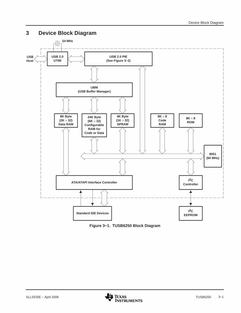
Device Block Diagram
3−1SLLS535E − April 2008 TUSB6250
3 Device Block Diagram24 MHz
USB 2.0UTMI
USBHost
USB 2.0 PIE(See Figure 3−2)
8K Byte(2K × 32)
Data RAM
4K Byte(1K × 32)SPRAM
24K Byte(6K × 32)
ConfigurableRAM for
Code or Data
UBM(USB Buffer Manager)
8K × 8CodeRAM
8051(60 MHz)
8K × 8ROM
I2CControllerATA/ATAPI Interface Controller
Standard IDE DevicesI2C
EEPROM
Figure 3−1. TUSB6250 Block Diagram

Device Block Diagram
3−2 SLLS535E − April 2008TUSB6250
Transaction Handler
Bus Monitor USB Reg. MCU
UBM(USB Buffer Manager)
Frame Timer
UTMI-CompliantPhy
Figure 3−2. USB 2.0 PIE (Parallel Interface Engine) Block Diagram

Device Parameter Information
4−1SLLS535E − April 2008 TUSB6250
4 Device Parameter Information
4.1 Pin Diagram
22 23
DD7DD8DD6DD9DGNDDD5DD10DVDDDD4DD11DD3DD12DGNDDD2DD13DVDDDD1DD14DD0DD15
60
59
58
57
56
55
54
53
52
51
50
49
48
47
46
45
44
43
42
4124
1
2
3
4
5
6
7
8
9
10
11
12
13
14
15
16
17
18
19
20
DVREGENRSTIP2.7
VBUSRPU
AVDDAGND
PLLVDD18UDVDD18
AGNDR1
VREGENAVDD
DPDM
AGNDXTAL2XTAL1
TSTMODE1TSTMODE2
25 26 27 28
TQFP PACKAGE(TOP VIEW)
79 78 77 76 7580 74 72 71 7073
29 30 31 32 33
69 68
21
67 66 65 64
34 35 36 37 38 39 40
63 62 61
SU
SP
EN
DP
3.0/
SIN
P3.
1/S
OU
TD
VD
DD
VD
D18
DG
ND
P2.
0P
3.2/
CD
1P
3.3/
CD
2P
3.4
P3.
5P
2.1/
PW
R10
0P
2.2/
PW
R50
0P
2.3
DG
ND
P2.
4P
2.5
DV
DD
P2.
6R
ST
_ATA
SC
LS
DA
DV
DD
P3.
7C
S1
CS
0D
GN
DD
A2
DA
0P
3.6
DA
1D
VD
D18
DV
DD
INT
RQ
DM
AC
KIO
RD
YD
GN
DD
IOR
DIO
WD
MA
RQ
Figure 4−1. Controller 80-Pin TQFP Pin Diagram

Device Parameter Information
4−2 SLLS535E − April 2008TUSB6250
4.2 Terminal Functions
Table 4−1. Controller Terminal Description (80-Pin TQFP)TERMINAL I/O
DESCRIPTIONNAME NO. TYPE NOTES
DESCRIPTION
INTEGRATED USB 2.0 UTMI-COMPLIANT PHY
AGND 7, 10,16
GND Analog ground. All ground terminals should be connected together externally through alow-impedance path. All bypass capacitors to PLLVDD18, UDVDD18, and AVDD should connect toground through a low-impedance path.
AVDD 6, 13 PWR 3.3-V supply voltage for the integrated USB 2.0 UTMI-compliant PHY’s internal analog circuitry. Thissupply is also regulated internally down to 1.8 V for use by the PHY’s internal digital circuitry whenVREGEN is asserted. Bypass capacitors to ground are required on these terminals.
DM 15 I/O USB differential data minus
DP 14 I/O USB differential data plus
PLLVDD18 8 PWR 1.8-V supply for the internal PLL circuitry of the integrated USB 2.0 UTMI-compliant PHY. An internalvoltage regulator generates this supply when terminal VREGEN is asserted. When VREGEN isde-asserted, 1.8 V must be supplied externally. Bypass capacitance is required on this terminalregardless of the state of VREGEN. It is recommended that the capacitance on this terminal not beless then 1 µF.
R1 11 I/O External reference resistor. An internally generated band-gap voltage is placed on this resistor. Thecurrent through the resistor is mirrored internally to generate the current and voltage used by theinternal analog circuitry. This pin has nominally 1.21 V dc. An external 5.9-kΩ ±1% resistor must beplaced between this terminal and ground. It is recommended that the resistor be placed as close aspossible to this terminal with a minimal trace length to ground.
RPU 5 I/O Pullup resistor connection. This terminal is used to attach and detach the full-speed indicator resistorelectrically to/from the DP signal line. An external 1.5-kΩ ±5% resistor must be placed between RPUand AVDD.
UDVDD18 9 PWR 1.92-V supply for the internal digital circuitry of the integrated USB 2.0 UTMI-compliant PHY. Aninternal voltage regulator generates this supply when terminal VREGEN is asserted. When VREGENis de-asserted, 1.92 V must be supplied externally. Bypass capacitance is required on this terminalregardless of the state of VREGEN. It is recommended that the capacitance on this terminal not beless then 1 µF. Do not connect the UDVDD18 terminal to the PLLVDD18 or DVDD18 terminal, becausetheir voltages differ.
VREGEN 12 I Voltage regulator enable (active-low). Two internal 3.3-V to 1.8-V voltage regulators supply the digitaland PLL circuitry when this terminal is asserted. When this terminal is de-asserted, the voltageregulators are disabled and 1.8 V must be supplied externally. TI recommends that this terminal betied to ground during normal operation.
CONTROLLER GENERAL
DVREGEN 1 I (4) This active-low terminal is used to enable the 3.3-V to 1.8-V voltage regulator in the TUSB6250’sdigital core. When this terminal is de-asserted, the voltage regulator is disabled and 1.8 V must besupplied externally. TI recommends that this terminal be tied to ground during normal operation.
P3.0/SIN 79 I/O (1)(6)(8)
This dual-function terminal can be used as either GPIO or the serial data input of the integrated 8051microcontroller serial port. The power-up default is to have its internal pullup activated.
P3.1/SOUT 78 I/O (1)(6)(8)
This dual-function terminal can be used as either GPIO or the serial data output of the integrated 8051microcontroller serial port. The power-up default is to have its internal pullup activated.
RSTI 2 I (4) The TUSB6250 master reset signal. This active-low terminal is the master reset signal for theTUSB6250. See Section 13.2, Reset Timing Reference, for detailed reset timing information.
SCL 21 O (7)(8) Master I2C controller: clock signal for external I2C serial EEPROM. The internal 100-µA pullup resistoron this terminal is always enabled.
SDA 22 I/O (4)(7)(8)
Master I2C controller: data signal for external I2C serial EEPROM. The internal 100-µA pullup resistoron this terminal is always enabled.
TSTMODE1TSTMODE2
1920
I (4)(8) These terminals are used for factory test of the TUSB6250. During normal operation, these terminalsmust be left open.
VBUS 4 I (5)(10) This terminal monitors the status of the USB upstream VBUS. It has the internal pulldown resistorenabled as the power-on reset default.
Device Parameter Information
4−3SLLS535E − April 2008 TUSB6250
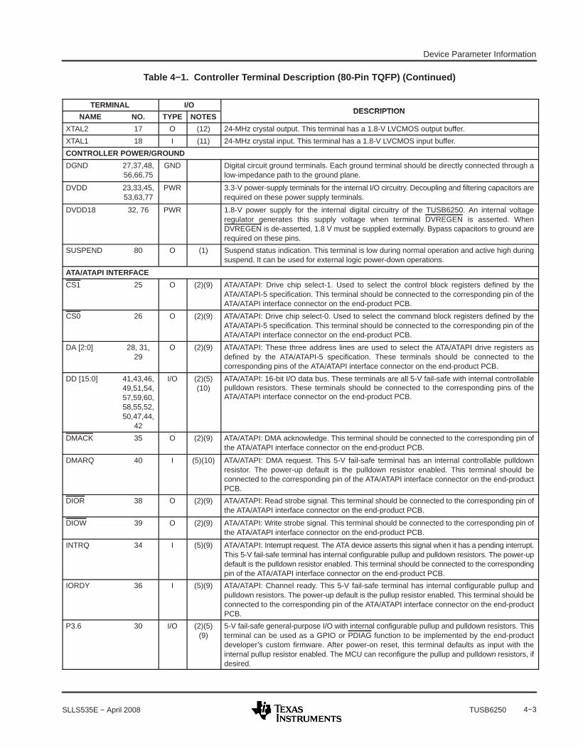
Table 4−1. Controller Terminal Description (80-Pin TQFP) (Continued)
TERMINAL I/ODESCRIPTION
NAME NO. TYPE NOTESDESCRIPTION
XTAL2 17 O (12) 24-MHz crystal output. This terminal has a 1.8-V LVCMOS output buffer.
XTAL1 18 I (11) 24-MHz crystal input. This terminal has a 1.8-V LVCMOS input buffer.
CONTROLLER POWER/GROUND
DGND 27,37,48,56,66,75
GND Digital circuit ground terminals. Each ground terminal should be directly connected through alow-impedance path to the ground plane.
DVDD 23,33,45,53,63,77
PWR 3.3-V power-supply terminals for the internal I/O circuitry. Decoupling and filtering capacitors arerequired on these power supply terminals.
DVDD18 32, 76 PWR 1.8-V power supply for the internal digital circuitry of the TUSB6250. An internal voltageregulator generates this supply voltage when terminal DVREGEN is asserted. WhenDVREGEN is de-asserted, 1.8 V must be supplied externally. Bypass capacitors to ground arerequired on these pins.
SUSPEND 80 O (1) Suspend status indication. This terminal is low during normal operation and active high duringsuspend. It can be used for external logic power-down operations.
ATA/ATAPI INTERFACE
CS1 25 O (2)(9) ATA/ATAPI: Drive chip select-1. Used to select the control block registers defined by theATA/ATAPI-5 specification. This terminal should be connected to the corresponding pin of theATA/ATAPI interface connector on the end-product PCB.
CS0 26 O (2)(9) ATA/ATAPI: Drive chip select-0. Used to select the command block registers defined by theATA/ATAPI-5 specification. This terminal should be connected to the corresponding pin of theATA/ATAPI interface connector on the end-product PCB.
DA [2:0] 28, 31,29
O (2)(9) ATA/ATAPI: These three address lines are used to select the ATA/ATAPI drive registers asdefined by the ATA/ATAPI-5 specification. These terminals should be connected to thecorresponding pins of the ATA/ATAPI interface connector on the end-product PCB.
DD [15:0] 41,43,46,49,51,54,57,59,60,58,55,52,50,47,44,
42
I/O (2)(5)(10)
ATA/ATAPI: 16-bit I/O data bus. These terminals are all 5-V fail-safe with internal controllablepulldown resistors. These terminals should be connected to the corresponding pins of theATA/ATAPI interface connector on the end-product PCB.
DMACK 35 O (2)(9) ATA/ATAPI: DMA acknowledge. This terminal should be connected to the corresponding pin ofthe ATA/ATAPI interface connector on the end-product PCB.
DMARQ 40 I (5)(10) ATA/ATAPI: DMA request. This 5-V fail-safe terminal has an internal controllable pulldownresistor. The power-up default is the pulldown resistor enabled. This terminal should beconnected to the corresponding pin of the ATA/ATAPI interface connector on the end-productPCB.
DIOR 38 O (2)(9) ATA/ATAPI: Read strobe signal. This terminal should be connected to the corresponding pin ofthe ATA/ATAPI interface connector on the end-product PCB.
DIOW 39 O (2)(9) ATA/ATAPI: Write strobe signal. This terminal should be connected to the corresponding pin ofthe ATA/ATAPI interface connector on the end-product PCB.
INTRQ 34 I (5)(9) ATA/ATAPI: Interrupt request. The ATA device asserts this signal when it has a pending interrupt.This 5-V fail-safe terminal has internal configurable pullup and pulldown resistors. The power-updefault is the pulldown resistor enabled. This terminal should be connected to the correspondingpin of the ATA/ATAPI interface connector on the end-product PCB.
IORDY 36 I (5)(9) ATA/ATAPI: Channel ready. This 5-V fail-safe terminal has internal configurable pullup andpulldown resistors. The power-up default is the pullup resistor enabled. This terminal should beconnected to the corresponding pin of the ATA/ATAPI interface connector on the end-productPCB.
P3.6 30 I/O (2)(5)(9)
5-V fail-safe general-purpose I/O with internal configurable pullup and pulldown resistors. Thisterminal can be used as a GPIO or PDIAG function to be implemented by the end-productdeveloper’s custom firmware. After power-on reset, this terminal defaults as input with theinternal pullup resistor enabled. The MCU can reconfigure the pullup and pulldown resistors, ifdesired.

Device Parameter Information
4−4 SLLS535E − April 2008TUSB6250
Table 4−1. Controller Terminal Description (80-Pin TQFP) (Continued)TERMINAL I/O
DESCRIPTIONNAME NO. TYPE NOTES
DESCRIPTION
P3.7 24 I/O (2)(5)(9)
5-V fail-safe general-purpose I/O with internal configurable pullup and pulldown resistors. This terminalcan be used as a GPIO or DASP function, which is implemented by the end-product developer’s customfirmware. After a power-on reset, this terminal defaults as input with the internal pullup resistor enabled.The MCU can reconfigure the pullup and pulldown resistors, if desired.
RST_ATA 61 O (2)(9) ATA/ATAPI: Asynchronous drive-reset signal. This terminal should be connected to the correspondingpin of the ATA/ATAPI interface connector on the end-product PCB.
OTHER GPIOs (GENERAL-PURPOSE I/Os)
P2.7 3 I/O (1)(6)(8)
General-purpose I/O with an internal controllable pullup resistor. After a power-on reset, this terminaldefaults as an input with an internal pullup resistor activated. The MCU can disable the pullup resistorif desired.
P2.6P2.5P2.4
626465
I/O (2)(5)(9)
5-V fail-safe general-purpose I/O with internal configurable pullup and pulldown resistors. Afterpower-on reset, these terminals default as inputs with the internal pullup resistor activated. The MCUcan reconfigure the pullup and pulldown resistors if desired.
P2.3 67 O (3) General-purpose open-drain output without internal pullup and pulldown resistors.
P2.2/PWR500
68 O (3) General-purpose open-drain output. This terminal can be controlled by the firmware to inform theATA/ATAPI device connected to the TUSB6250 that the end-product device (including the TUSB6250itself) is allowed to draw 500 mA from the USB after the device is fully enumerated and configured asa USB-powered device.
P2.1/PWR100
69 O (3) General-purpose open-drain output. During the USB enumeration phase, This terminal is asserted bythe boot code to inform the ATA/ATAPI device connected to the TUSB6250 that the end-product device(including the TUSB6250 itself) is allowed to draw 100 mA from the USB. After the boot coderelinquishes control to the firmware when USB enumeration, configuration, and firmware download arefinished, the firmware can reconfigure the function of this terminal for other usage, as long as suchusage is not conflicting with the previous usage, which, for example, can be implemented in the endproduct for power sequencing control purposes. It should be noted that, for self-powered applications,if VBUS from the USB is not present (for example, the USB cable is not connected) during boot time,the boot code does not assert this terminal. In this condition, it is the responsibility of firmware to assertthis terminal, once the firmware is downloaded and gains control.
P2.0 74 I/O (2)(5)(9)
5-V fail-safe general-purpose I/O with internal configurable pullup and pulldown resistors. Afterpower-on reset, this terminal defaults as an input with the internal pulldown resistor activated. The MCUcan reconfigure the pullup and pulldown resistors if desired.
P3.5P3.4
7071
I/O (2)(5)(9)
5-V fail-safe general-purpose I/O with internal configurable pullup and pulldown resistors. Afterpower-on reset, these terminals default as inputs with an internal pullup resistor activated. The MCUcan reconfigure the pullup and pulldown resistors, if desired. These two terminals can be used asremote wake-up event inputs. The end-product developer’s custom firmware can use these twoterminals to implement some end-product-specific functions, such as cartridge insertion detection,eject button pressed, or external control input to request the end-product custom firmware to put theTUSB6250’s ATA/ATAPI bus into the high-impedance state.
P3.3/CD2P3.2/CD1
7273
I/O (2)(5)(9)
5-V fail-safe general-purpose I/O with internal configurable pullup and pulldown resistors. Afterpower-on reset, these terminals default as inputs with an internal pullup resistor activated. The MCUcan reconfigure the pullup and pulldown resistors, if desired. These terminals can be used as GPIOsor compact flash card insertion/removal detection inputs implemented by the end-product developer’scustom firmware. These terminals are remote wake-up capable inputs, if enabled.
NOTES: 1. 3-state 3.3-V LVCMOS output (±8-mA drive/sink).2. 3-state 3.3-V LVCMOS output, 5-V fail-safe (±8-mA drive/sink). The 5-V fail-safe means this output buffer can be exposed to a 5-V
application environment. Although it can not output 5 V when interfacing with the 5-V ATA/ATAPI device, an external pullup resistorto a 5-V power source can be used to pull the output voltage up to 5 V. The fail-safe buffer is designed to be protected from damageunder a condition where the buffer is exposed to 5 V, while the device is powered down (its supply voltage is zero).
3. Open-drain output (8-mA sink), 5-V fail-safe, without internal pullup and pulldown resistors.4. 3.3-V LVCMOS hysteresis input.5. TTL-compatible, 5-V fail-safe, hysteresis input.6. 3.3-V LVCMOS input without hysteresis.7. Open-drain output (4-mA sink) with an internal pullup resistor.8. Internal 100-µA active pullup resistor.9. Configurable internal 200-µA active pullup and pulldown resistors.
10. Controllable internal 200-µA active pulldown resistor11. 1.8-V LVCMOS input buffer12. 1.8-V LVCMOS output buffer

Device Parameter Information
4−5SLLS535E − April 2008 TUSB6250
4.3 Device Operation
4.3.1 Device Master Reset
An external master reset signal, asynchronous to the TUSB6250 internal clock, is needed to reset theTUSB6250. This reset is referred to as the power-on reset throughout this document, which is connected tothe RSTI terminal of the TUSB6250. Because the TUSB6250 has built-in noise debouncing circuitry, it alsorequires a valid clock signal present during the required active-low master reset window. For the details of themaster reset timing requirement, see Section 13.2, Reset Timing Reference.
4.3.2 Clock Generation
The TUSB6250 requires an external 24-MHz crystal to be used. The integrated USB 2.0 UTMI-compliant PHYgenerates all of the clock signals needed for the PHY analog, PLL, and digital logic. The PHY also generatesa 60-MHz clock used in the internal digital core of the TUSB6250.
4.3.3 Device Initialization
Because the TUSB6250 contains an integrated MCU, the device initialization process contains the followingtwo parts:
• Hardware registers and state machines are cleared to their defined default reset state after power-on resetinitialization. The TUSB6250 powers up with a default USB function address of zero and is disconnectedfrom the USB bus.
• The MCU executes a bootloader program in ROM (starting from address 0000h) to fetch the validapplication code from the external source and prepare for USB enumeration. The application code, oncein charge, may perform some initialization functions to configure the TUSB6250 to meet the requirementof a particular end-product application.
Because the application code (firmware) space is in the internal RAM, the TUSB6250 firmware needs to bedownloaded from an external source into the RAM space designated for code usage (see Section 6.1, MCUMemory Map, for detailed information).
After power-on reset is applied to the TUSB6250, the integrated MCU executes the bootloader program (alsoreferred as boot code) residing in the on-chip 8K-byte ROM mapped to the MCU program memory space; thisprocess is also referred to as booting.
The major tasks of the boot code are:
• To fetch the descriptors required for itself or the firmware to perform USB enumeration
• To download the application firmware from one of the two external sources available during booting: eitherfrom an external I2C EEPROM connected to the I2C interface of the TUSB6250 or from the host PC viathe USB bus connection
The MCU executes a read from an external I2C EEPROM and checks whether it contains valid applicationcode by comparing the read value with the expected boot signature. If it contains valid code, the MCU executesfollow-up reads from the EEPROM and writes the code into the TUSB6250 internal 32K bytes of default codeRAM. If the external EEPROM does not contain any valid code, the MCU proceeds to boot from the USB.
The I2C EEPROM normally is preprogrammed with a valid application code image. It also contains all theconfigurable USB descriptors and other configurable descriptors or parameters for the mass storage deviceconnected to the TUSB6250 ATA/ATAPI interface. For the option of booting from the USB host, the applicationcode may reside in the host PC. However, the external I2C EEPROM is still needed to store the USB 2.0specification-required vendor ID and product ID specific to each individual end-product manufacturer.

Device Parameter Information
4−6 SLLS535E − April 2008TUSB6250
Depending on the type of firmware used as specified in the header block of the external I2C EEPROM, theboot code can determine:
• Whether to perform connection to the USB host for enumeration before downloading the firmware into theinternal code RAM
• Whether to remain disconnected during the firmware code downloading process. In this case, thefirmware, once in charge, assumes the responsibility of performing the connect and enumeration tasks.
For details on how to specify the header block of the external I2C EEPROM, booting, and enumeration options,see the TUSB6250 Bootcode Application Note application report (SLLA126).

Architecture Overview
5−1SLLS535E − April 2008 TUSB6250
5 Architecture Overview
The overall functionality of the TUSB6250 is achieved by the combined interaction of major blocks orsubcontrollers as shown earlier in Figure 3−1. These major blocks include the USB 2.0 UTMI-compliant PHY,USB 2.0 parallel interface engine (PIE), embedded microcontroller unit (MCU), USB buffer manager (UBM),ATA/ATAPI interface controller, and the I2C interface controller.
5.1 Controller Brief Data Flow
As shown in Figure 5−1, the USB host controller, residing inside a PC, issues commands and/or data to theTUSB6250-based external USB 2.0 mass storage device. The TUSB6250’s internal data flow is describedas follows (out-transaction example):
1. The USB 2.0 UTMI-compliant PHY receives serial data, either high-speed or full-speed, from the externalupstream USB host controller. The PHY processes this serial data stream and converts it into the8-bit-wide parallel data packet based on the protocol defined in the USB 2.0 specification and the UTMIspecification.
2. The 8-bit wide parallel data packet, switching at 60-MHz, is passed to the USB 2.0 PIE block. The USB2.0 PIE processes the data based on the defined USB packet protocol and passes the data to the UBMblock.
3. The UBM performs the endpoint address decoding and then passes the data packet to the addressed databuffer location, which is either the endpoint buffer space or the sector FIFO space configured by the MCUand its firmware. The section FIFO is the dedicated data buffer space directly accessible by the TUSB6250controller’s internal high-performance ATA/ATAPI interface controller. The UBM also generates theappropriate interrupt to inform the MCU of the arrival of the new packet.
4. The embedded MCU, either moves the data manually between the endpoint buffer and the ATA/ATAPIinterface, or enables automatic data movement between the sector FIFO and the ATA/ATAPI interface.
5. If the automatic data movement path is enabled, the data packet targeted to the storage device is loadedautomatically from the UBM into sector FIFO.
6. The ATA/ATAPI interface controller, which is a high-performance DMA engine, automatically moves thedata from sector FIFO to the storage device connected to its ATA/ATAPI interface with the data transferprotocol and timing configured by the MCU and the firmware.
USBHost
TUSB6250ATA or ATAPI
Drive
Figure 5−1. TUSB6250 Typical Application Diagram

Architecture Overview
5−2 SLLS535E − April 2008TUSB6250
5.2 Overview of Major Function Blocks
5.2.1 USB 2.0 UTMI-Compliant PHY
The main functions of the integrated USB 2.0 UTMI-compliant PHY are to convert the received serial datastream from the USB host controller into parallel data packets that can be processed by the controller engineof the TUSB6250 and to perform parallel-to-serial conversion for the data packets to be transmitted to the USBhost.
The integrated PHY communicates to the TUSB6250 controller parallel interface engine (PIE) through twoseparate 8-bit-wide transmit and receive data buses and other handshake signals defined in the USB 2.0UTMI specification version 1.4. The PHY also provides a 60-MHz clock signal to the PIE for synchronization.It supports both high-speed (480 Mbps) USB signaling and full-speed (12 Mbps) signaling. This backwardcompatibility allows the TUSB6250 controller to connect to any legacy USB full-speed hosts and hubs.
The PHY includes circuitry to monitor the line conditions for determining connection status, initialization, andpacket reception and transmission. The integrated PHY requires only an external 24-MHz crystal as areference. An external clock, with 1.8-V magnitude, can be provided to the XTAL1 pin instead of a crystal. Aninternal oscillator drives an internal phase-locked loop (PLL), which generates the required 480-MHzreference clock. The reference clock is internally divided to provide the clock signals used to control theinternal receive and transmit circuitry. The suspend function stops the operation of the PLL.
Data bits to be transmitted upstream are received on the 8-bit transmit bus from the PIE of the TUSB6250controller and latched in synchronization with the 60-MHz clock. These bits are combined serially, encodedand bit-stuffed as required, and transmitted to the USB host. During packet reception, the transmitters aredisabled. A clock signal and serial data bits are recovered from the received NRZI-encoded and bit-stuffedinformation. The serial data bits are bit unstuffed, NRZI decoded, and deserialized. These bits are thenresynchronized to the local 60-MHz clock and sent to the PIE on the 8-bit wide receive bus.
The integrated PHY also provides the 60-MHz clock source to be used on all other blocks of the TUSB6250controller. It contains two 3.3-V to 1.8-V voltage regulators to supply power for the PHY internal digital andPLL circuitry.
An external 1.5-kΩ ±5% resistor must be placed between the RPU and AVDD pins. The resistor is requiredfor full-speed indication and connect signaling. Another external 5.9-kΩ ±1% resistor must be placed betweenR1 and ground, which is used to mirror the current for internal analog circuitry reference.
5.2.2 USB 2.0 Parallel Interface Engine (PIE)
As shown in Figure 3−2, the PIE consists of four major blocks: a frame timer, a bus a monitor, a transactionhandler, and USB registers.
The bus monitor, as its name implies, monitors the USB differential signal line status through the USB 2.0UTMI-compliant PHY. It informs the MCU via updating the UTMICFG:UTMI configuration status register(XDATA at F00A) with the current line status information, such as high-speed or full-speed mode indication,VBUS status, idle, and SE0 detection information. While interfacing with the PHY, the bus monitor is able toperform connect or disconnect according to the configuration set up by the MCU and firmware. It detects andgenerates the USB full-speed or high-speed handshake based on the protocol defined in the USB 2.0specification and provides other capabilities such as suspend, resume, and remote wakeup. The bus monitoralso supports the required USB 2.0 high-speed compliance test modes.
The frame timer is responsible for tracking starts of frames (SOFs) from the bus monitor and generating theUSB frame number and microframe number, which is described in Section 8.6, USBFCL: USB Frame CounterLow-Byte Register (XDATA at F00B) and Section 8.7, USBFCH: USB Frame Counter High-Byte Register(XDATA at F00C).

Architecture Overview
5−3SLLS535E − April 2008 TUSB6250
The transaction handler manages the USB packet protocol requirement for the packets being received andtransmitted on the USB by the TUSB6250. For the received packet, the transaction handler checks the packetidentifier (PID) field to reveal the correct packet type from those defined by the USB 2.0 specification, suchas token, data, handshake, and special packets. It then checks the address, endpoint number, and the CRCto ensure the received packet is a valid one being addressed to one of the enabled endpoints in the TUSB6250controller. If the received packet is a data packet, it first notifies the UBM with the endpoint address anddirection information of the incoming data packet and then passes the following data payload. For the packetbeing transmitted, the transaction handler gets the data from the UBM and generates the correct PID and CRCas part of the transmit packet to be transmitted along with the data payload to the USB host. Thesynchronization field (SYNC) is generated by the PHY. For the handshake packet, the UBM tells thetransaction handler what kind of handshake packet to send, as long as the CRC is valid. The transactionhandler then performs the task of sending the required handshake packet.
5.2.3 USB Buffer Manager (UBM)
The UBM is a high-performance DMA engine that manages the data movement between the transactionhandler and the TUSB6250 endpoint data buffer or sector FIFO (used by the ATA/ATAPI interface controllerfor high-speed data transfer between the TUSB6250 controller and the storage device connected to itsATA/ATAPI interface). For received packets, the UBM checks the endpoint address, direction information, andloads (writes) the data payload into the appropriate endpoint data buffer or sector FIFO in the TUSB6250controller. For the packet being transmitted, the UBM decodes the valid endpoint address, directioninformation from the token packet provided by the transaction handler, and performs a read from the correctendpoint data buffer or sector FIFO location in the TUSB6250 controller. The read-data is then passed to thetransaction handler to be processed and transferred to the USB host.
5.2.4 Embedded Microcontroller Unit (MCU)
The integrated MCU in the TUSB6250 controller is a high-speed 8-bit microcontroller core based on theindustry standard 8051 with certain improvements. The MCU operates at 60-MHz clock frequency with up to30 MIPS performance.
The main functionality of the embedded MCU core of the TUSB6250 controller is to serve as a centralprocessing platform to allow the boot code (the microcode running at boot time) and firmware to perform thedevice configuration and the activity control function by configuring and updating all the registers in the MCU,USB, ATA/ATAPI, I2C, and the GPIO blocks.
5.2.5 ATA/ATAPI Interface Controller
The ATA/ATAPI interface controller is a high-performance DMA engine that continuously monitors the statusand manages the data movement between sector FIFO and the ATA/ATAPI storage device connected to theTUSB6250 ATA/ATAPI interface, based on the ATA/ATAPI timing and protocol defined by the ATA/ATAPI-5specification.
The ATA/ATAPI interface controller of the TUSB6250 controller offers both the flexibility of general MCU-basedbridge controllers and the performance of state-machine-based bridge controllers. It allows the MCU to movethe data manually between the endpoint data buffer and the ATA/ATAPI interface, while providing ahigh-performance automatic data movement mode, in which the ATA/ATAPI interface controller and the UBMwork together to move the data quickly among the UBM, sector FIFO, and the ATA/ATAPI interface withoutMCU involvement during the data stage of the bulk-only data transfer.
Some of the flexibilities offered by the TUSB6250 ATA/ATAPI interface controller include:
• Firmware-configurable IDE data transfer modes and timing that can be configured in the resolution of the60-MHz clock cycle period
• Many hardware registers that provide information to assist the MCU to handle all 13 case conditionscorrectly defined by the USB mass storage bulk-only transfer protocol specification.

Architecture Overview
5−4 SLLS535E − April 2008TUSB6250
5.2.6 I2C Interface Controller
The master-only I2C interface controller is responsible for acquiring the user-configurable descriptors andother configurable feature parameters from the external I2C EEPROM during initial power up. It is also usedto download the application firmware from the external I2C EEPROM. The behavior of the I2C interfacecontroller is controlled by the boot code (the microcode embedded in boot ROM) or application firmware.
5.3 Other Major Features
5.3.1 Unique Power-On Sequencing to the Storage Device
The TUSB6250 provides unique power-on sequencing features to the storage device. When the TUSB6250is powered up during the reset period, it turns off all the output buffers and activates all of the internal pulldownresistors on the ATA/ATAPI bus. After reset, when the TUSB6250 controller is enumerated and configured,the application firmware in operation decides when to power up the connected ATA/ATAPI drive andreconfigure all the input, output, and bidirectional buffers, and the pullup and pulldown resistors on theATA/ATAPI bus based on their functionality defined in the ATA/ATAPI-5 specification.
This function is critical for implementing a truly bus-powered USB 2.0 mass storage device, because the diskstart-up spinning normally results in a high-current surge that is harmful to the USB device during enumeration.According to the USB 2.0 specification, a USB device is only allowed to consume up to 100 mA before it isconfigured.
This feature is also useful when the TUSB6250 controller interfaces to ATA/ATAPI mass storage devices thatdo not implement fail-safe buffers on their ATA/ATAPI interface. In such conditions, this well controlledpower-on sequencing feature protects the connected storage device without fail-safe I/O buffers from damagethat might be caused by the bridge controller driving the signal lines when the power supply of the storagedevices is not present.
5.3.2 Die-ID Based USB Device Serial Number
The TUSB6250 supports unique USB device serial numbers by using the 48-bit die-ID number unique to eachsilicon die. It also allows end-product developers to specify their own custom serial number in the external I2CEEPROM to override this default die-ID serial number.

Microcontroller Unit (MCU)
6−1SLLS535E − April 2008 TUSB6250
6 Microcontroller Unit (MCU)
The embedded MCU is a high-performance version (8051 Warp core) of the standard 8-bit 8051microcontroller, requiring just two clocks per machine cycle, while keeping functional compatibility with thestandard part. This allows the embedded MCU to run up to six times faster than the standard part for the samepower consumption. The ratio of two clock cycles to one machine cycle is constant across the instruction setand all addressing modes, so as to maintain instruction execution-time compatibility with other devices.
The MCU is the central processing unit controlling the overall activity of the TUSB6250 controller with theapplication firmware, which is loaded into the TUSB6250 controller’s internal embedded code RAM spacefrom either the external I2C EEPROM or the USB host in a PC.
The MCU, with its firmware, through accessing all the related USB and ATA/ATAPI registers, can configurethe USB functions of the TUSB6250 controller, such as the characteristics of endpoints, remote wakeupcapability, low-power-enable feature, interrupts to MCU, GPIO configuration, etc. It also configures theATA/ATAPI interface controller behavior, such as the mode of the TUSB6250 controller’s internal datamovement, ATA/ATAPI interface data transfer modes, and timing.
6.1 MCU Memory Map
The industry standard 8051 microcontroller normally organizes its complete memory space into three majorcategories: program memory, internal data memory, and external data memory. Following this convention, theembedded MCU memory space of the TUSB6250 controller is referred to throughout this data manual as:
• Program memory is also referred to as the code space.
• Internal data memory refers to the 1152 bytes of IDATA memory.
• External data memory refers to the internal XDATA space, including the MMRs and 4K-byte data buffersof the EDB, because the data memory, although integrated in this device, is external to the embeddedMCU core.
Figure 6−1 illustrates the MCU memory map. Note that the internal IDATA space is not shown, because it isallocated in the same location as the standard 8051 microcontroller (starting from 0x00 hex). The enhancedIDATA memory embedded in the TUSB6250 controller, with a size of 1152 bytes, can be used for multitaskingfirmware to speed up execution.
The shaded areas represent the internal ROM/RAM.
• The 8K bytes of ROM containing the boot code are mapped to address range 0x0000−0x1FFF.
• The 8K bytes of RAM (fixed as code space for application firmware) are mapped to address range0x2000−0x3FFF.
• The other 8K bytes of RAM (fixed as sector FIFO), as shown in the unshaded area enclosed with the dottedline, are directly accessible by the internal ATA/ATAPI interface controller.
• The 4K-byte data buffers of the end point descriptor block (EDB) are mapped to address range(E000−EFFF), which are implemented by the single-port RAM (SPRAM).
• Memory-mapped registers (MMRs) and other buffers are mapped to address range (F000−F0F9) and areall implemented by registers. The MMRs include registers used for USB, I2C, ATA/ATAPI interfaceconfiguration, GPIO, pullup/pulldown control, etc.
• The actual configuration of the middle 24K bytes of RAM (4000−9FFF), which are part of the 40K bytesof configurable RAM for code and data space, depends on the RAMPARTN bits in the MODECNFGregister.
− After power up, RAMPARTN = 00 is the default. This configures the 24K bytes RAM as code spacewith the address mapped to 4000−9FFF and yields total 32K bytes of code RAM from 2000−9FFF

Microcontroller Unit (MCU)
6−2 SLLS535E − April 2008TUSB6250
addressable by the MCU and 8K bytes of RAM for the sector FIFO data space that is not directlyaccessible by the MCU.
− The MCU can change this power-up RAM configuration by overwriting the value of the RAMPARTNbits. Thus, reconfiguring this 24K bytes of RAM as part of the code space or sector FIFO data spacecan be accomplished per the firmware instruction setting:
• RAMPARTN = 01, this yields a total of 16K bytes of code RAM from 2000−5FFF accessible bythe MCU and 24K bytes of RAM for sector FIFO not directly accessible by the MCU, but directlyaccessible by the internal ATA/ATAPI interface controller.
• RAMPARTN = 10, this yields a total of 8K bytes of code RAM from 2000−3FFF accessible by theMCU and 32K bytes of RAM for sector FIFO not directly accessible by the MCU, but directlyaccessible by the internal ATA/ATAPI interface controller.
8K BytesROM
0000
1FFF
8K BytesRAM
(Fixed for Code)
2000
3FFF
24K BytesRAM
(Configurablefor Code orSector FIFOData Space)
4000
5FFF
6000
7FFF
8000
9FFF
4K BytesSPRAM
E000
EFFF
MMRF000
F0F9
00 01 10
Code/Data Space Partition Result Basedon the Setting of the RAMPARTN Bits
32K BytesRAM
For Code
16K BytesRAM
For Code
8K BytesRAM
For Code
8K BytesRAM
For Data
24K BytesRAM
For Data
32K BytesRAM
For Data
A000
BFFF
Figure 6−1. MCU Memory Map

Microcontroller Unit (MCU)
6−3SLLS535E − April 2008 TUSB6250
6.2 Internal XDATA Space [E000 → F0F9]
The address range from E000 to F0F9 in XDATA space is reserved for data buffers and MMRs.
• Data buffers of the EDB are all allocated in the address range E000 to EFFF, which are implemented bySPRAM.
• MMRs can be allocated in the address range F000 to FFFF, which are implemented by registers. MMRscontain all endpoint descriptor blocks (EDB) registers, which as the name implies, are used by the MCUto configure and access each endpoint in the TUSB6250 controller.
Table 6−1 represents the XDATA space allocation and access restriction for the UBM and the MCU.
Table 6−2 describes the complete MMR memory map.
Table 6−1. XDATA Space Map [E000 → F0F9]DESCRIPTION ADDRESS RANGE UBM ACCESS MCU ACCESS
E000
Data buffersData buffersof the EDB
(4K SPRAM)Yes Yesof the EDB
(4K SPRAM)Yes Yes
EFFF
F000
Internal MMRsInternal MMRs(memory mapped registers) See Notes 1 and 2 Yes(memory mapped registers) See Notes 1 and 2 Yes
F0F9
NOTES: 1. The UBM can access all EDB registers in MMRs needed for current endpoint access.2. The UBM cannot access anything else other than EDBs in MMRs.

Microcontroller Unit (MCU)
6−4 SLLS535E − April 2008TUSB6250
Table 6−2. Memory Mapped Registers Summary (XDATA Range: F000 → F0F9)ADDRESS REGISTER NAME DESCRIPTION
F000 IEPCNFG_0 Input endpoint_0 configuration register
F001 IEPBCN_0 Input endpoint_0 buffer byte count register
F002 Reserved
F003 OEPCNFG_0 Output endpoint_0 configuration register
F004 OEPBCN_0 Output endpoint_0 buffer byte count register
F005 Reserved
F006 USBCTL USB control register
F007 USBMSK USB interrupt mask register
F008 USBSTA USB status register
F009 FUNADR Function address register
F00A UTMICFG UTMI configuration status register
F00B USBFCL USB frame counter low-byte register
F00C USBFCH USB frame counter high-byte register
F00D USBWKUP USB wakeup reason register
F00E Reserved
F00F Reserved
F010 IEPCNFG_1 Input endpoint_1 configuration register
F011 IEPBBADRX_1 Input endpoint_1 X buffer base address register
F012 IEPBCNLX_1 Input endpoint_1 X buffer byte count low-byte register
F013 IEPBCNHX_1 Input endpoint_1 X buffer byte count high-byte register
F014 IEPSIZXY_1 Input endpoint_1 X/Y buffer size register
F015 IEPBBADRY_1 Input endpoint_1 Y buffer base address register
F016 IEPBCNLY_1 Input endpoint_1 Y buffer byte count low-byte register
F017 IEPBCNHY_1 Input endpoint_1 Y buffer byte count high-byte register
F018 OEPCNFG_1 Output endpoint_1 configuration register
F019 OEPBBADRX_1 Output endpoint_1 X buffer base address register
F01A OEPBCNLX_1 Output endpoint_1 X buffer byte count low-byte register
F01B OEPBCNHX_1 Output endpoint_1 X buffer byte count high-byte register
F01C OEPSIZXY_1 Output endpoint_1 X/Y buffer size register
F01D OEPBBADRY_1 Output endpoint_1 Y buffer base address register
F01E OEPBCNLY_1 Output endpoint_1 Y buffer byte count low-byte register
F01F OEPBCNHY_1 Output endpoint_1 Y buffer byte count high-byte register
F020 IEPCNFG_2 Input endpoint_2 configuration register
F021 IEPBBADRX_2 Input endpoint_2 X buffer base address register
F022 IEPBCNLX_2 Input endpoint_2 X buffer byte count low-byte register
F023 IEPBCNHX_2 Input endpoint_2 X buffer byte count high-byte register
F024 IEPSIZXY_2 Input endpoint_2 X/Y buffer size register
F025 IEPBBADRY_2 Input endpoint_2 Y buffer base address register
F026 IEPBCNLY_2 Input endpoint_2 Y buffer byte count low-byte register
F027 IEPBCNHY_2 Input endpoint_2 Y buffer byte count high-byte register

Microcontroller Unit (MCU)
6−5SLLS535E − April 2008 TUSB6250
Table 6−2. Memory Mapped Registers Summary (XDATA Range: F000 → F0F9) (Continued)
ADDRESS REGISTER NAME DESCRIPTION
F028 OEPCNFG_2 Output endpoint_2 configuration register
F029 OEPBBADRX_2 Output endpoint_2 X buffer base address register
F02A OEPBCNLX_2 Output endpoint_2 X buffer byte count low-byte register
F02B OEPBCNHX_2 Output endpoint_2 X buffer byte count high-byte register
F02C OEPSIZXY_2 Output endpoint_2 X/Y buffer size register
F02D OEPBBADRY_2 Output endpoint_2 Y buffer base address register
F02E OEPBCNLY_2 Output endpoint_2 Y buffer byte count low-byte register
F02F OEPBCNHY_2 Output endpoint_2 Y buffer byte count high-byte register
F030 IEPCNFG_3 Input endpoint_3 configuration register
F031 IEPBBADRX_3 Input endpoint_3 X buffer base address register
F032 IEPBCNLX_3 Input endpoint_3 X buffer byte count low-byte register
F033 IEPBCNHX_3 Input endpoint_3 X buffer byte count high-byte register
F034 IEPSIZXY_3 Input endpoint_3 X/Y buffer size register
F035 IEPBBADRY_3 Input endpoint_3 Y buffer base address register
F036 IEPBCNLY_3 Input endpoint_3 Y buffer byte count low-byte register
F037 IEPBCNHY_3 Input endpoint_3 Y buffer byte count high-byte register
F038 OEPCNFG_3 Output endpoint_3 configuration register
F039 OEPBBADRX_3 Output endpoint_3 X buffer base address register
F03A OEPBCNLX_3 Output endpoint_3 X buffer byte count low-byte register
F03B OEPBCNHX_3 Output endpoint_3 X buffer byte count high-byte register
F03C OEPSIZXY_3 Output endpoint_3 X/Y buffer size register
F03D OEPBBADRY_3 Output endpoint_3 Y buffer base address register
F03E OEPBCNLY_3 Output endpoint_3 Y buffer byte count low-byte register
F03F OEPBCNHY_3 Output endpoint_3 Y buffer byte count high-byte register
F040 IEPCNFG_4 Input endpoint_4 configuration register
F041 IEPBBADRX_4 Input endpoint_4 X buffer base address register
F042 IEPBCNLX_4 Input endpoint_4 X buffer byte count low-byte register
F043 IEPBCNHX_4 Input endpoint_4 X buffer byte count high-byte register
F044 IEPSIZXY_4 Input endpoint_4 X/Y buffer size register
F045 IEPBBADRY_4 Input endpoint_4 Y buffer base address register
F046 IEPBCNLY_4 Input endpoint_4 Y buffer byte count low-byte register
F047 IEPBCNHY_4 Input endpoint_4 Y buffer byte count high-byte register
F048 OEPCNFG_4 Output endpoint_4 configuration register
F049 OEPBBADRX_4 Output endpoint_4 X buffer base address register
F04A OEPBCNLX_4 Output endpoint_4 X buffer byte count low-byte register
F04B OEPBCNHX_4 Output endpoint_4 X buffer byte count high-byte register
F04C OEPSIZXY_4 Output endpoint_4 X/Y buffer size register
F04D OEPBBADRY_4 Output endpoint_4 Y buffer base address register
F04E OEPBCNLY_4 Output endpoint_4 Y buffer byte count low-byte register
F04F OEPBCNHY_4 Output endpoint_4 Y buffer byte count high-byte register
F050 Reserved
↓ Reserved
F07F Reserved
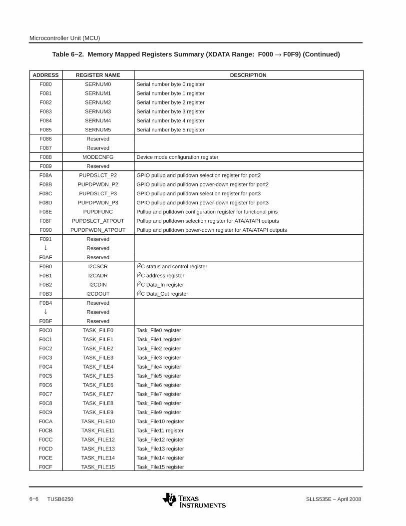
Microcontroller Unit (MCU)
6−6 SLLS535E − April 2008TUSB6250
Table 6−2. Memory Mapped Registers Summary (XDATA Range: F000 → F0F9) (Continued)
ADDRESS REGISTER NAME DESCRIPTION
F080 SERNUM0 Serial number byte 0 register
F081 SERNUM1 Serial number byte 1 register
F082 SERNUM2 Serial number byte 2 register
F083 SERNUM3 Serial number byte 3 register
F084 SERNUM4 Serial number byte 4 register
F085 SERNUM5 Serial number byte 5 register
F086 Reserved
F087 Reserved
F088 MODECNFG Device mode configuration register
F089 Reserved
F08A PUPDSLCT_P2 GPIO pullup and pulldown selection register for port2
F08B PUPDPWDN_P2 GPIO pullup and pulldown power-down register for port2
F08C PUPDSLCT_P3 GPIO pullup and pulldown selection register for port3
F08D PUPDPWDN_P3 GPIO pullup and pulldown power-down register for port3
F08E PUPDFUNC Pullup and pulldown configuration register for functional pins
F08F PUPDSLCT_ATPOUT Pullup and pulldown selection register for ATA/ATAPI outputs
F090 PUPDPWDN_ATPOUT Pullup and pulldown power-down register for ATA/ATAPI outputs
F091 Reserved
↓ Reserved
F0AF Reserved
F0B0 I2CSCR I2C status and control register
F0B1 I2CADR I2C address register
F0B2 I2CDIN I2C Data_In register
F0B3 I2CDOUT I2C Data_Out register
F0B4 Reserved
↓ Reserved
F0BF Reserved
F0C0 TASK_FILE0 Task_File0 register
F0C1 TASK_FILE1 Task_File1 register
F0C2 TASK_FILE2 Task_File2 register
F0C3 TASK_FILE3 Task_File3 register
F0C4 TASK_FILE4 Task_File4 register
F0C5 TASK_FILE5 Task_File5 register
F0C6 TASK_FILE6 Task_File6 register
F0C7 TASK_FILE7 Task_File7 register
F0C8 TASK_FILE8 Task_File8 register
F0C9 TASK_FILE9 Task_File9 register
F0CA TASK_FILE10 Task_File10 register
F0CB TASK_FILE11 Task_File11 register
F0CC TASK_FILE12 Task_File12 register
F0CD TASK_FILE13 Task_File13 register
F0CE TASK_FILE14 Task_File14 register
F0CF TASK_FILE15 Task_File15 register

Microcontroller Unit (MCU)
6−7SLLS535E − April 2008 TUSB6250
Table 6−2. Memory Mapped Registers Summary (XDATA Range: F000 → F0F9) (Continued)
ADDRESS REGISTER NAME DESCRIPTION
F0D0 ATPIFCNFG0 ATA/ATAPI interface configuration register 0
F0D1 ATPIFCNFG1 ATA/ATAPI interface configuration register 1
F0D2 ATPACSREG0 ATA/ATAPI access register 0
F0D3 ATPACSREG1 ATA/ATAPI access register 1
F0D4 ATPACSREG2 ATA/ATAPI access register 2
F0D5 ATPACSREG3 ATA/ATAPI access register 3
F0D6 TRANSBCNT0 USB or ATA/ATAPI transfer byte count register 0 (7:0)
F0D7 TRANSBCNT1 USB or ATA/ATAPI transfer byte count register 1 (15:8)
F0D8 TRANSBCNT2 USB or ATA/ATAPI transfer byte count register 2 (23:16)
F0D9 TRANSBCNT3 USB or ATA/ATAPI transfer byte count register 3 (31:24)
F0DA CMNDLNGTH Command length register
F0DB BLKSECCNT Block sector count register
F0DC PIOSPAS PIO transfer speed (assertion timing) register
F0DD PIOSPRC PIO transfer speed (recovery timing) register
F0DE DMASPAS DMA transfer speed (assertion timing) register
F0DF DMASPRC DMA transfer speed (recovery timing) register
F0E0 MCUBYTE0 MCU data byte_0 register
F0E1 MCUBYTE1 MCU data byte_1 register
F0E2 MCUBYTE2 MCU data byte_2 register
F0E3 MCUBYTE3 MCU data byte_3 register
F0E4 MCUACSL MCU access address low-byte register
F0E5 MCUACSH MCU access address high-byte register
F0E6 ATPINTRPT0 ATA/ATAPI interrupt register 0
F0E7 ATPINTMSK0 ATA/ATAPI interrupt mask register 0
F0E8 ATPINTRPT1 ATA/ATAPI interrupt register 1
F0E9 ATPINTMSK1 ATA/ATAPI interrupt mask register 1
F0EA ATPSTATUS ATA/ATAPI interface status register
F0EB SECWRPTL Sector FIFO write pointer low-byte register
F0EC SECWRPTH Sector FIFO write pointer high-byte register
F0ED WRPTBKUPL Sector FIFO write pointer backup low-byte register
F0EE WRPTBKUPH Sector FIFO write pointer backup high-byte register
F0EF SECRDPTL Sector FIFO read pointer low-byte register
F0F0 SECRDPTH Sector FIFO read pointer high-byte register
F0F1 RDPTBKUPL Sector FIFO read pointer backup low-byte register
F0F2 RDPTBKUPH Sector FIFO read pointer backup high-byte register
F0F3 Reserved
↓ Reserved
F0F8 Reserved
F0F9 ULRCVEXCNT Ultra receive extra word count register

Microcontroller Unit (MCU)
6−8 SLLS535E − April 2008TUSB6250
6.3 MCU Control and Status Registers (in SFR and ESFR Space)
This section describes the PCON register (in standard 8051 SFR space) and all the registers added to thestandard 8051 special function registers (SFRs) space in the TUSB6250 controller. These added registersare referred to as extended special function registers (ESFRs).
For information regarding the standard SFRs, see the industry-standard 8051 specification. Table 6−3outlines the standard and extended 8051 registers in the IDATA space.
Table 6−3. SFR Map [IDATA: 0x80 → 0xFF]DESCRIPTION LABEL ADDRESS
Port 0 P0 80
Stack pointer SP 81
Data pointer LB DPL 82
Data pointer HB DPH 83
Power control register PCON 87
Timer/counter control TCON 88
Timer/counter mode TMOD 89
Timer/counter 0 LB TL0 8A
Timer/counter 1 LB TL1 8B
Timer/counter 0 HB TH0 8C
Timer/counter 1 HB TH1 8D
Port 1 P1 90
Serial control register SCOM 98
Serial data buffer SBUF 99
Port 2 P2 A0
Interrupt enable register IE A8
Port 3 P3 B0
Interrupt priority register IP B8
Break point status register BPSTA BD
Break point register 1 (LB) (see Note 1) BPL1 BE
Break point register 1 (HB) PBH1 BF
Reserved (see Note 2) C0
Break point register 2 (LB) BPL2 C1
Break point register 2 (HB) PBH2 C2
Reserved C3
Break point register 3 (LB) BPL3 C4
Break point register 3 (HB) PBH3 C5
Reserved C6
Break point register 4 (LB) BPL4 C7
Break point register 4 (HB) PBH4 C8
Reserved C9
Jump-to-monitor address register (LB) JTML CA
Jump-to-monitor address register (HB) JTMH CB
Reserved CC
Reserved CD
Stack break point register SBK CE
Break point control register BPCRL CF
Program status word PSW D0

Microcontroller Unit (MCU)
6−9SLLS535E − April 2008 TUSB6250
Table 6−3. SFR Map [IDATA: 80 FF] (Shaded Area Indicates ESFRs) (Continued)
DESCRIPTION LABEL ADDRESS
D1 → DF is used for scratch pad (see Note 3) D1 → DF
Accumulator A E0
Interrupt enable register 1 IE1 E8
B register B F0
RTK timer register RTKTM F6
Vector interrupt register VECINT F7
Interrupt priority register 1 IP1 F8
PC copy register (LB) PCL F9
PC copy register (HB) PCH FA
Watchdog timer CSR WDCSR FB
MCU configuration register MCUCNFG FC
Power-on reset and suspend detection register PWONSUSP FD
Reserved FE
Reserved FF
NOTES: 1. ESFRs (BE−CF) are write-protected when LJMP to the application is executed. When LJMP to the monitor is executed or when MCUwrites 55h to the BPSTA register, these registers become unprotected.
2. Application firmware should not write to any space marked as Reserved.3. These locations are reserved as the monitor working area and applications should not use them.
6.3.1 PCON: Power Control Register (at SFR 87h)
The PCON is the standard 8051 power control register. The PCON register is cleared by a power-up resetor a watchdog timer (WDT) reset. The PCON register can also be cleared by a USB reset when the functionreset connection bit in the USBCTL register is set (FRSTE = 1).
7 6 5 4 3 2 1 0
SMOD RSV RSV RSV GF1 FG0 RSV IDL
R/W R/O R/O R/O R/W R/W R/O R/W
BIT NAME RESET FUNCTION
0 IDL 0 MCU idle mode bit. This bit can be set by the MCU and is cleared by the assertion of any enabledinterrupt. It is not recommended to use the MCU idle mode during normal operation of the TUSB6250controller.
1 RSV 0 Reserved = 0
3−2 GF [1:0] 00 General-purpose bits. The MCU can write and read these bits.
6−4 RSV 0000 Reserved = 0
7 SMOD 0 Double-baud-rate control bit. For more information see the UART serial interface in the M8051 corespecification.
6.3.2 RTKTM: RTK Timer Register (at ESFR F6h)
The RTK timer counter is a down counter with its initial value loaded from the RTK timer value specified in theRTKTM register. A 10-µs clock is used for the RTK timer counter. When the value in the down counter reacheszero, an interrupt pulse is generated (connected to INT6) and the RTKTM value is reloaded into the counter.This register provides an interrupt period of 10 µs to 2550 µs. Any write to this counter clears the originalcontent of the counter and causes the counter to restart the down count from the new timer value.
The RTKTM register is cleared by a power-up reset or a WDT reset. The RTKTM register can also be clearedby a USB reset when the function reset connection bit in the USBCTL register is set (FRSTE = 1).

Microcontroller Unit (MCU)
6−10 SLLS535E − April 2008TUSB6250
7 6 5 4 3 2 1 0
T7 T6 T5 T4 T3 T2 T1 T0
R/W R/W R/W R/W R/W R/W R/W R/W
BIT NAME RESET FUNCTION
7−0 T [7:0] 00h RTK timer value. The RTKTM register defines the RTK (INT6) interrupt intervals in 10 µsincrements. Note that a INT6 interrupt is generated only when T[7:0]>00 and EI6 is set (E16=1) inthe IE1: interrupt enable register (SFR at E8).00h = RTK timer is disabled.01h = Interrupt is generated every 10 µs02h = Interrupt is generated every 20 µs:FFh = Interrupt is generated every 2,550 µs
6.3.3 WDCSR: Watchdog Timer Control and Status Register (at ESFR FBh)A watchdog timer (WDT) with a 1-ms clock is provided. If the WDCSR register is not accessed for a periodof 128 ms, the WDT counter resets the MCU. When debugger logic is enabled and a break is detected, theWDT is suspended until a jump-to-application is executed. at such point, the WDT resumes operation.
The WDT is enabled by default and can only be disabled by the MCU/firmware writing a pattern of 101010into the WDD [5:0] bits. To avoid accidental reset by the WDT, the firmware has to ensure that it clears the WDTbefore going into suspend.
The WDCSR register is cleared by a power-up reset only. The USB reset cannot clear the WDCSR register.
7 6 5 4 3 2 1 0
WDRI WDD5 WDD4 WDD3 WDD2 WDD1 WDD0 WDCES
R/C R/W R/W R/W R/W R/W R/W R/W
BIT NAME RESET FUNCTION
0 WDCES 1 Watchdog timer counter clear and enabling status.• For write access, this bit acts as the watchdog timer counter clear bit. The MCU must write a 1 to
this bit to prevent the WDT from resetting the device. If the MCU does not write a 1 in a period of128 ms, the WDT resets the device. Writing a 0 has no effect on the WDT. The WDT is an 8-bitcounter using a 1-ms CLK.
• For read access, this bit acts as a status bit to indicate whether the watchdog timer is currentlyenabled. A return value of 1 indicates the watchdog timer is enabled and a return value of 0indicates the watchdog timer is disabled. A reset value of 1 indicates the watchdog timer is enabledby default.
6−1 WDD[5:0] 000000 These bits are used to disable the watchdog timer. For the timer to be disabled, these bits must be setto a special pattern of 101010. If any other pattern is present, the watchdog timer remains in operation.These bits are read back as all 0.
7 WDRI 0 Watchdog reset indication bit. This bit indicates if the reset occurred due to a power-up reset or awatchdog timer reset.WDR = 0 A power-up reset occurred.WDR = 1 A watchdog timeout reset occurred. To clear this bit, the MCU must write a 1. Writing a 0 has no effect.
6.3.4 MCUCNFG: MCU Configuration Register (at ESFR FCh)The APP_MODE bit (bit 0) provides an indication for the MCU to distinguish whether it is currently runningin the boot-sequence mode or under firmware control. Once the boot code finishes the firmware downloadand is ready to switch to firmware control, it sets this bit before relinquishing the control to the firmware. Thefirmware should take extra care and never clear this bit.
When the WAKCLK bit in the USBMSK register and any one of the bits (bit 5 to 2) of the MCUCNFG registerare both enabled, any status change (for example, a media insertion/ejection or other remote wakeup event)on the GPIO pins related to these four bits triggers a WAKCLK interrupt to the MCU, while the source of thestatus change is logged in the USB wakeup reason register. Bits [5:2] act as the individual status change(event) enable bits.

Microcontroller Unit (MCU)
6−11SLLS535E − April 2008 TUSB6250
For some removable media reader applications, if the media connector has connector detection pins at twoopposite sides of the connector (for example, card reader application for compact flash card or PCMCIA typeII card/drive), both CD1STEN and CD2STEN must be enabled to ensure correct detection of media insertion.
The MCUCNFG register is cleared by a power-up reset or a WDT reset. A USB reset cannot reset theMCUCNFG register.
7 6 5 4 3 2 1 0
RSV RSV CD2STEN CD1STEN P35STEN P34STEN RSV APP_MODE
R/O R/O R/W R/W R/W R/W R/O R/W
BIT NAME RESET FUNCTION
0 APP_MODE 0 Application mode. This bit indicates whether the device is running under boot code or firmwarecontrol. The firmware should take extra care and never clear this bit.APP_MODE = 0 The TUSB6250 is running in the boot sequence mode.APP_MODE = 1 The TUSB6250 is running under firmware control.
1 RSV 0 Reserved
2 P34STEN 0 P3.4 status change detection enable.P34STEN = 0 Disable pin P3.4 status change detectionP34STEN = 1 Enable pin P3.4 status change detection
3 P35STEN 0 P3.5 status change detection enable.P35STEN = 0 Disable pin P3.5 status change detectionP35STEN = 1 Enable pin P3.5 status change detection
4 CD1STEN 0 Card/media detection−1 enable.CD1STEN = 0 Disable card/media CD1 status detectionCD1STEN = 1 Enable card/media CD1 status detection
5 CD2STEN 0 Card/media detection−2 enable.CD2STEN = 0 Disable card/media CD2 status detectionCD2STEN = 1 Enable card/media CD2 status detection
7−6 RSV 00 Reserved
6.3.5 PWONSUSP: Power-On Reset and Suspend Detection Register (at ESFR FDh)
The POSP bit of the PWONSUSP register provides a way to let the target ATA/ATAPI device distinguishbetween a power-up reset and a remote wakeup (or resume). The MCU can set the POSP bit when it decidesto go into suspend.
The BANKSEL bits are used by the MCU to select one of the eight IDATA memory banks when running in amultitasking environment to speed up code execution. Figure 6−2 shows the IDATA space multibank memoryconfiguration map.
The PWONSUSP register is cleared by a power-up reset or a WDT reset. A USB reset cannot reset thePWONSUSP register.

Microcontroller Unit (MCU)
6−12 SLLS535E − April 2008TUSB6250
7 6 5 4 3 2 1 0
RSV RSV RSV RSV BANKSEL2 BANKSEL1 BANKSEL0 SCRATCH
R/O R/O R/O R/O R/W R/W R/W R/W
BIT NAME RESET FUNCTION
0 SCRATCH 0 This is a scratch bit that can be read and written by the MCU for any end-product-specificfunction, if supported by the end-product custom firmware.
One of the recommended usages can be defined as a bit to indicate to the applicationfirmware whether the power-up sequence that occurred on the ATA/ATAPI device wascaused by a remote wakeup, resume from suspend, or a power-up reset. This can beachieved by the MCU writing a 1 to this bit before going into suspend.
3−1 BANKSEL[2:0]
000 IDATA bank select.The MCU can write to BANKSEL to select a particular bank in one of the eight IDATA bankspaces. Each bank has a capacity of 256 bytes with the middle 128 bytes shared with theother banks.
7−4 RSV 0h Reserved = 0h
Internal Data MemoryBank 0
(256 × 8 Bit)
00
3F
Nonshared Space64 Bytes
C0
FF
Nonshared Space64 Bytes
40
BF
Internal Data MemoryBank N (N = 1 − 7)
(256 × 8 Bit)
Nonshared Space64 Bytes
Nonshared Space64 Bytes
Shared Space128 Bytes
Figure 6−2. IDATA Space Memory Configuration
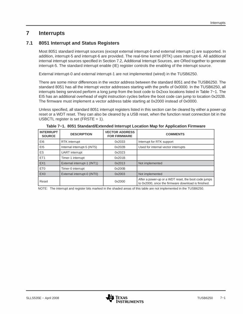
Interrupts
7−1SLLS535E − April 2008 TUSB6250
7 Interrupts
7.1 8051 Interrupt and Status Registers
Most 8051 standard interrupt sources (except external interrupt-0 and external interrupt-1) are supported. Inaddition, interrupt-5 and interrupt-6 are provided. The real-time kernel (RTK) uses interrupt-6. All additionalinternal interrupt sources specified in Section 7.2, Additional Interrupt Sources, are ORed together to generateinterrupt-5. The standard interrupt enable (IE) register controls the enabling of the interrupt source.
External interrupt-0 and external interrupt-1 are not implemented (wired) in the TUSB6250.
There are some minor differences in the vector address between the standard 8051 and the TUSB6250. Thestandard 8051 has all the interrupt vector addresses starting with the prefix of 0x0000. In the TUSB6250, allinterrupts being serviced perform a long jump from the boot code to 0x2xxx locations listed in Table 7−1. TheEI5 has an additional overhead of eight instruction cycles before the boot code can jump to location 0x202B.The firmware must implement a vector address table starting at 0x2000 instead of 0x0000.
Unless specified, all standard 8051 interrupt registers listed in this section can be cleared by either a power-upreset or a WDT reset. They can also be cleared by a USB reset, when the function reset connection bit in theUSBCTL register is set (FRSTE = 1).
Table 7−1. 8051 Standard/Extended Interrupt Location Map for Application FirmwareINTERRUPT
SOURCE DESCRIPTIONVECTOR ADDRESS
FOR FIRMWARE COMMENTS
EI6 RTK interrupt 0x2033 Interrupt for RTK support
EI5 Internal interrupt-5 (INT5) 0x202B Used for internal vector interrupts
ES UART interrupt 0x2023
ET1 Timer-1 interrupt 0x201B
EX1 External interrupt-1 (INT1) 0x2013 Not implemented
ET0 Timer-0 interrupt 0x200B
EX0 External interrupt-0 (INT0) 0x2003 Not implemented
Reset 0x2000After a power-up or a WDT reset, the boot code jumpsto 0x2000, once the firmware download is finished.
NOTE: The interrupt and register bits marked in the shaded areas of this table are not implemented in the TUSB6250.

Interrupts
7−2 SLLS535E − April 2008TUSB6250
7.1.1 IE: Interrupt Enable Register (SFR at A8)
7 6 5 4 3 2 1 0
EA RSV EI5 ES ET1 RSV ETO RSV
R/W R/O R/W R/W R/W R/O R/W R/O
BIT NAME RESET FUNCTION
0 RSV 0 Reserved
1 ET0 0 Enable or disable timer-0 interrupt.ET0 = 0 Timer-0 interrupt is disabledET0 = 1 Timer-0 interrupt is enabled
2 RSV 0 Reserved
3 ET1 0 Enable or disable timer-1 interrupt.ET1 = 0 Timer-1 interrupt is disabledET1 = 1 Timer-1 interrupt is enabled
4 ES 0 Enable or disable serial port interrupts.ES = 0 Serial port interrupt is disabledES = 1 Serial port interrupt is enabled
5 EI5 0 Used for all internal interrupts.EI5 = 0 INT5 is disabledEI5 = 1 INT5 is enabled
6 RSV 0 Reserved
7 EA 0 Enable or disable all interrupts (global disable).EA = 0 Disable all interruptsEA = 1 Each interrupt source is individually controlled
7.1.2 IP: Interrupt Priority Register (SFR at B8)
7 6 5 4 3 2 1 0
RSV RSV PI5 PS PT1 RSV PT0 RSV
R/O R/O R/W R/W R/W R/O R/W R/O
BIT NAME RESET FUNCTION
0 RSV 0 Reserved
1 PT0 0 Selects ET0 priority.PT0 = 0 Low priorityPT0 = 1 High priority
2 RSV 0 Reserved
3 PT1 0 Selects ET1 priority.PT1 = 0 Low priorityPT1 = 1 High priority
4 PS 0 Selects ES priority.PS = 0 Low priorityPS = 1 High priority
5 PI5 0 Selects EI5 priority.PI5 = 0 Low priorityPI5 = 1 High priority
7−6 RSV 00 Reserved

Interrupts
7−3SLLS535E − April 2008 TUSB6250
7.1.3 IE1: Interrupt Enable Register (SFR at E8)
7 6 5 4 3 2 1 0
RSV RSV RSV RSV RSV RSV RSV EI6
R/O R/O R/O R/O R/O R/O R/O R/W
BIT NAME RESET FUNCTION
0 EI6 0 Enable or disable RTK interrupt.EI6 = 0 RTK interrupt is disabledEI6 = 1 RTK interrupt is enabled
7−1 RSV 0 Reserved
7.1.4 IP1: Interrupt Priority Register (SFR at F8)
7 6 5 4 3 2 1 0
RSV RSV RSV RSV RSV RSV RSV PI6
R/O R/O R/O R/O R/O R/O R/O R/W
BIT NAME RESET FUNCTION
0 PI6 0 Selects EI6 priority.EI6 = 0 Low priorityEI6 = 1 High priority
7−1 RSV 0000 000 Reserved
7.1.5 TCON: Timer/Counter Control Register (SFR at 88)
The TCON register is the standard 8051 TCON register.
7 6 5 4 3 2 1 0
TF1 TR1 TF0 TR0 RSV RSV RSV RSV
R/W R/W R/W R/W R/O R/O R/O R/O
BIT NAME RESET FUNCTION
3−0 RSV 0h Reserved
4 TR0 0 Timer-0 control bitTR0 = 0 Timer is halted.TR0 = 1 Timer is running.
5 TF0 0 Timer-0 overflow flagTF0 = 0 Cleared by hardware when the MCU calls the interrupt routineTF0 = 1 Set by hardware when the timer overflows
6 TR1 0 Timer-1 control bitTR1 = 0 Timer is halted.TR1 = 1 Timer is running.
7 TF1 0 Timer-1 overflow flagTF1 = 0 Cleared by hardware when the MCU calls the interrupt routineTF1 = 1 Set by hardware when the timer overflows
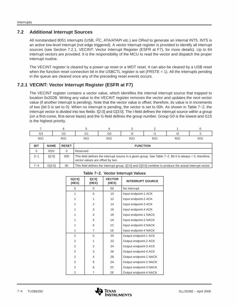
Interrupts
7−4 SLLS535E − April 2008TUSB6250
7.2 Additional Interrupt Sources
All nonstandard 8051 interrupts (USB, I2C, ATA/ATAPI etc.) are ORed to generate an internal INT5. INT5 isan active low-level interrupt (not edge triggered). A vector interrupt register is provided to identify all interruptsources (see Section 7.2.1, VECINT: Vector Interrupt Register (ESFR at F7), for more details). Up to 64interrupt vectors are provided. It is the responsibility of the MCU to read the vector and dispatch the properinterrupt routine.
The VECINT register is cleared by a power-up reset or a WDT reset. It can also be cleared by a USB resetwhen the function reset connection bit in the USBCTL register is set (FRSTE = 1). All the interrupts pendingin the queue are cleared once any of the preceding reset events occurs.
7.2.1 VECINT: Vector Interrupt Register (ESFR at F7)
The VECINT register contains a vector value, which identifies the internal interrupt source that trapped tolocation 0x202B. Writing any value to the VECINT register removes the vector and updates the next vectorvalue (if another interrupt is pending). Note that the vector value is offset; therefore, its value is in incrementsof two (bit 0 is set to 0). When no interrupt is pending, the vector is set to 00h. As shown in Table 7−2, theinterrupt vector is divided into two fields: I[2:0] and G[3:0]. The I-field defines the interrupt source within a group(on a first-come, first-serve basis) and the G-field defines the group number. Group G0 is the lowest and G15is the highest priority.
7 6 5 4 3 2 1 0
G3 G2 G1 G0 I2 I1 I0 0
R/O R/O R/O R/O R/O R/O R/O R/O
BIT NAME RESET FUNCTION
0 RSV 0 Reserved
3−1 I[2:0] 000 This field defines the interrupt source in a given group. See Table 7−2. Bit 0 is always = 0, therefore,vector values are offset by two.
7−4 G[3:0] 0h This field defines the interrupt group. I[2:0] and G[3:0] combine to produce the actual interrupt vector.
Table 7−2. Vector Interrupt ValuesG[3:0](HEX)
I[2:0](HEX)
VECTOR(HEX) INTERRUPT SOURCE
0 0 00 No interrupt
1 0 10 Input endpoint-1 ACK
1 1 12 Input endpoint-2 ACK
1 2 14 Input endpoint-3 ACK
1 3 16 Input endpoint-4 ACK
1 4 18 Input endpoint-1 NACK
1 5 1A Input endpoint-2 NACK
1 6 1C Input endpoint-3 NACK
1 7 1E Input endpoint-4 NACK
2 0 20 Output endpoint-1 ACK
2 1 22 Output endpoint-2 ACK
2 2 24 Output endpoint-3 ACK
2 3 26 Output endpoint-4 ACK
2 4 28 Output endpoint-1 NACK
2 5 2A Output endpoint-2 NACK
2 6 2C Output endpoint-3 NACK
2 7 2E Output endpoint-4 NACK

Interrupts
7−5SLLS535E − April 2008 TUSB6250
Table 7−2. Vector Interrupt Values (Continued)
G [3:0](HEX)
I [2:0](HEX)
VECTOR(HEX) INTERRUPT SOURCE
3 0 30 STPOW packet received
3 1 32 SETUP packet received
3 2 34 RESR interrupt
3 3 36 SUSPR interrupt
3 4 38 RSTR interrupt
3 5−7 3A−3E Not used
4 0 40 Input endpoint-0 ACK
4 1 42 Output endpoint-0 ACK
4 2 44 Input endpoint-0 NACK
4 3 46 Output endpoint-0 NACK
4 4 48 ATA interrupt
4 5 4A WAKCLK interrupt
4 6−7 4C → 4E Not used
5−15 X 90 → FE Not used

Interrupts
7−6 SLLS535E − April 2008TUSB6250
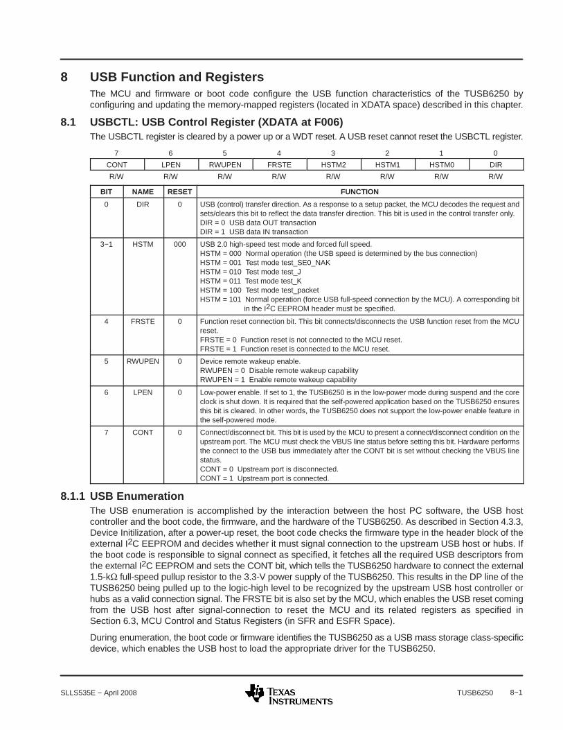
8−1SLLS535E − April 2008 TUSB6250
8 USB Function and RegistersThe MCU and firmware or boot code configure the USB function characteristics of the TUSB6250 byconfiguring and updating the memory-mapped registers (located in XDATA space) described in this chapter.
8.1 USBCTL: USB Control Register (XDATA at F006)The USBCTL register is cleared by a power up or a WDT reset. A USB reset cannot reset the USBCTL register.
7 6 5 4 3 2 1 0
CONT LPEN RWUPEN FRSTE HSTM2 HSTM1 HSTM0 DIR
R/W R/W R/W R/W R/W R/W R/W R/W
BIT NAME RESET FUNCTION
0 DIR 0 USB (control) transfer direction. As a response to a setup packet, the MCU decodes the request andsets/clears this bit to reflect the data transfer direction. This bit is used in the control transfer only.DIR = 0 USB data OUT transactionDIR = 1 USB data IN transaction
3−1 HSTM 000 USB 2.0 high-speed test mode and forced full speed.HSTM = 000 Normal operation (the USB speed is determined by the bus connection)HSTM = 001 Test mode test_SE0_NAKHSTM = 010 Test mode test_JHSTM = 011 Test mode test_KHSTM = 100 Test mode test_packetHSTM = 101 Normal operation (force USB full-speed connection by the MCU). A corresponding bit
in the I2C EEPROM header must be specified.
4 FRSTE 0 Function reset connection bit. This bit connects/disconnects the USB function reset from the MCUreset.FRSTE = 0 Function reset is not connected to the MCU reset.FRSTE = 1 Function reset is connected to the MCU reset.
5 RWUPEN 0 Device remote wakeup enable.RWUPEN = 0 Disable remote wakeup capabilityRWUPEN = 1 Enable remote wakeup capability
6 LPEN 0 Low-power enable. If set to 1, the TUSB6250 is in the low-power mode during suspend and the coreclock is shut down. It is required that the self-powered application based on the TUSB6250 ensuresthis bit is cleared. In other words, the TUSB6250 does not support the low-power enable feature inthe self-powered mode.
7 CONT 0 Connect/disconnect bit. This bit is used by the MCU to present a connect/disconnect condition on theupstream port. The MCU must check the VBUS line status before setting this bit. Hardware performsthe connect to the USB bus immediately after the CONT bit is set without checking the VBUS linestatus.CONT = 0 Upstream port is disconnected.CONT = 1 Upstream port is connected.
8.1.1 USB EnumerationThe USB enumeration is accomplished by the interaction between the host PC software, the USB hostcontroller and the boot code, the firmware, and the hardware of the TUSB6250. As described in Section 4.3.3,Device Initilization, after a power-up reset, the boot code checks the firmware type in the header block of theexternal I2C EEPROM and decides whether it must signal connection to the upstream USB host or hubs. Ifthe boot code is responsible to signal connect as specified, it fetches all the required USB descriptors fromthe external I2C EEPROM and sets the CONT bit, which tells the TUSB6250 hardware to connect the external1.5-kΩ full-speed pullup resistor to the 3.3-V power supply of the TUSB6250. This results in the DP line of theTUSB6250 being pulled up to the logic-high level to be recognized by the upstream USB host controller orhubs as a valid connection signal. The FRSTE bit is also set by the MCU, which enables the USB reset comingfrom the USB host after signal-connection to reset the MCU and its related registers as specified inSection 6.3, MCU Control and Status Registers (in SFR and ESFR Space).
During enumeration, the boot code or firmware identifies the TUSB6250 as a USB mass storage class-specificdevice, which enables the USB host to load the appropriate driver for the TUSB6250.

8−2 SLLS535E − April 2008TUSB6250
The following are some important notes regarding the USBCTL register.
• The contents of this register are not affected by the USB reset.
• The signaling connect/disconnect is totally controlled by the boot code or firmware by setting/clearing theCONT bit of this register. The TUSB6250 hardware does not perform any automatic action for this function.
8.1.2 USB Reset
The TUSB6250 can detect a USB reset condition. When a USB reset occurs, the TUSB6250 responds bysetting the function reset request (RSTR) bit in the USB status register (see USBSTA: USB status register(XDATA at F008), Section 8.2). If the corresponding function reset interrupt enable (RSTR) bit in theUSBMSDK: USB interrupt mask register (XDATA at F007), is set, an MCU interrupt is generated and the USBfunction reset (0x38) vector appears in the vector interrupt register (see VECINT: Vector Interrupt Register(ESFR at F7), Section 7.2.1).
8.1.3 USB 2.0 Test Mode
The USB 2.0 specification defines some additional high-speed test modes. The USB 2.0 test mode functionimplemented in the TUSB6250 is accomplished by both hardware and firmware. The MCU and firmware areresponsible for decoding the test mode commands from the USB host and then selecting one of the four testmodes based on the command received by setting the HSTM bits in the USBCTL register. Additional detailsregarding the hardware and firmware behaviors in the test mode are described below:
• HSTM = 001 (Test_SE0_NAK): The TUSB6250 hardware only treats this mode as a normal operationmode and does not perform any special test-mode function. The firmware must set NAK bits to 1 so thatthe hardware can behave as Test_SE0_NAK defined and respond to any IN token packet with a NAKhandshake, as long as the packet CRC is correct.
• HSTM = 010 (Test Mode Test_J): The TUSB6250 hardware automatically performs the required task inthis test mode. The firmware only must set HSTM bits to initiate the test.
• HSTM = 011 (Test Mode Test_K): The TUSB6250 hardware automatically performs the required task inthis test mode. The firmware only must set this bit to initiate the test.
• HSTM = 100 (Test Mode Test_Packet): The TUSB6250 hardware supports this mode; however, it requiresthe firmware to load the data payload into the X-buffer of IN-endpoint-0 and specify the byte-countinformation. The hardware sends the packet repetitively.

8−3SLLS535E − April 2008 TUSB6250
8.2 USBMSK: USB Interrupt Mask Register (XDATA at F007)
Bits[5:0] of the USBMSK register provide a mechanism to allow the MCU and firmware to enable or disablethe generation of certain types of interrupts based on the corresponding status or events that occurred.
The USBMSK register is cleared by a power up or a WDT reset. A USB reset cannot reset the USBMSKregister.
7 6 5 4 3 2 1 0
RSV RSV RSTR SUSPR RESUR WAKCLK SETUP STPOW
R/O R/O R/W R/W R/W R/W R/W R/W
BIT NAME RESET FUNCTION
0 STPOW 0 SETUP overwrite interrupt enable bitSTPOW = 0 STPOW interrupt disabledSTPOW = 1 STPOW interrupt enabled
1 SETUP 0 SETUP interrupt enable bitSETUP = 0 SETUP interrupt disabledSETUP = 1 SETUP interrupt enabled
2 WAKCLK 0 Wakeup clock interrupt enable.WAKCLK = 0 Wakeup clock interrupt disabledWAKCLK = 1 Wakeup clock interrupt enabled
3 RESUR 0 Function resume interrupt enableRESUR = 0 Function resume interrupt disabledRESUR = 1 Function resume interrupt enabled
4 SUSPR 0 Function suspend interrupt enableSUSPR = 0 Function suspend interrupt disabledSUSPR = 1 Function suspend interrupt enabled
5 RSTR 0 Function reset interrupt enableRSTR = 0 Function reset interrupt disabledRSTR = 1 Function reset interrupt enabled
7−6 RSV 00 Reserved. Application firmware must ensure these 2 bits are set to 00 during normal operation.

8−4 SLLS535E − April 2008TUSB6250
8.3 USBSTA: USB Status Register (XDATA at F008)
Each bit in the USBSTA register can generate an interrupt if its corresponding mask bit is set in the USBMSKregister. The related interrupt is cleared when the corresponding status bit is cleared by the MCU except theWAKCLK interrupt. All bits in this register are set by the hardware and can only be cleared by the MCU bywriting a 1 to the proper bit location (writing a 0 has no effect).
The USBSTA register (excluding the RSTR bit) is cleared by a power-up reset or a WDT reset. It can also becleared by a USB reset, when the function reset connection bit in the USBCTL register is set (FRSTE = 1).
The RSTR bit of the USBSTA register can only be cleared by a power-up reset or a WDT reset. A USB resetsets this bit to 1.
7 6 5 4 3 2 1 0
RSV RSV RSTR SUSPR RESUR WAKCLK SETUP STPOW
R/O R/O R/C R/C R/C R/C R/C R/C
BIT NAME RESET FUNCTION
0 STPOW 0 SETUP overwrite bit. Set by the hardware when the setup packet is received, while there is alreadya packet in the setup buffer. The MCU clears this bit by writing a 1 (writing 0 has no effect).
1 SETUP 0 SETUP transaction received bit. As long as SETUP is 1, IN and OUT on endpoint-0 are NAKed,regardless of their real NAK bits value. The MCU clears this bit by writing a 1 (writing 0 has no effect).
2 WAKCLK 0 Wakeup clock request bit. When WAKCLK interrupt is enabled, this bit is set in response to the statuschange on any of these pins: VBUS, P3.4, P3.5, CD1, or CD2. The interrupt generated due to this bitin turn wakes up the core clock if it has been shut down during suspend, when the remote wakeup isenabled.WAKCLK = 0 No wakeup clock event (status change on the five GPIO pins) is detected since the last
time the MCU clears the related status-change bit in USBWKUP.WAKCLK = 1 Wakeup clock event (any status change on the five GPIO pins) is detected since the
last time the MCU clears the related status-change bit in USBWKUP.
3 RESUR 0 Function resume request bit. The MCU clears this bit by writing a 1 (writing 0 has no effect).RESUR = 0 No function resume is detected.RESUR = 1 Function resume is detected.
4 SUSPR 0 Function suspended request bit. This bit is set in response to a global or selective suspend condition.The MCU clears this bit by writing a 1 (writing 0 has no effect).SUSPR = 0 No function suspend is detected.SUSPR = 1 Function suspend is detected.
5 RSTR 0 Function reset request bit. This bit is set in response to the host initiating a port reset to the TUSB6250.The USB function reset is the condition to set this bit, not clear this bit. The MCU clears this bit by writinga 1 (writing 0 has no effect).RSTR = 0 No function reset is detected.RSTR = 1 Function reset is detected.
6−7 RSV 00 Reserved = 0
8.3.1 USB Suspend
The USB 2.0 specification requires that all USB devices must support the suspend state. The USB devicesbegin the transition to the suspend state after they see a constant idle state on their upstream facing bus linesfor more than 3 ms. The device must actually be suspended, drawing only suspend current from the bus afterno more than 10 ms of bus inactivity on its port. The specification also requires that a device with remotewakeup capability may not generate resume signaling, unless the bus has been continuously in the idle statefor 5 ms.
In other words, the specification allows all USB devices to enter suspend at any time between 3 ms to 10 msafter bus idle. For USB high-speed capable devices, because there is an additional 0.125-ms revert-wait timefrom high-speed to full-speed after 3-ms high-speed bus idle, the actual time to enter suspend is between3.125 ms and 10 ms.

8−5SLLS535E − April 2008 TUSB6250
For the TUSB6250, the timing to enter the USB suspend is controlled by the application firmware running onthe embedded MCU. This flexibility allows the firmware to delay the time to go into suspend when the MCUis currently busy on some tasks that must be finished before the suspend.
Because the firmware controls the time to enter the suspend, in order to be compliant with USB 2.0specification, it is firmware responsibility to ensure that it clears the SUSPR interrupt status bit before 10 msexpires.
The normal procedure during the bus idle and suspend condition is described as follows:
1. The TUSB6250 hardware detects 3-ms bus idle.
2. If the current USB bus connection is full speed, the TUSB6250 hardware sets the SUSPR bit in theUSBSTA register and generates an SUSPR (function suspend request) interrupt to the MCU.
If the current USB bus connection is high-speed, the TUSB6250 hardware reverts back to a full-speedconnection within 0.125 ms, then sets the SUSPR bit and generates the SUSPR interrupt.
3. The firmware can check whether there is any task that must be finished before the suspend and performsit if desired. The firmware must ensure it grants the suspend request before 10 ms expires.
4. Once the firmware is ready to enter suspend, it clears the SUSPR bit in the USBSTA register. TheTUSB6250 hardware shuts the clock down (if LPEN = 1) and enters the suspend state.
8.3.2 WAKCLK Interrupt and Remote Wakeup
8.3.2.1 WAKCLK Interrupt Behavior
Figure 8−1 illustrates how the WAKCLK interrupt and WAKCLK status-change events are generated andcleared. The top portion of the diagram shows how each of the WAKCLK status-change events causes theWAKCLK bit in the USBSTA register to be set, if the WAKCLK interrupt is enabled in the USBMSK register(for illustration purpose, WAKCLK_en = 1 in Figure 8−1 implies WAKCLK = 1 in USBMSK). TheVBUSCHG_det and the other three status-change event detection signals are generated internally by theTUSB6250 hardware, whenever a WAKCLK status-change event occurs on the VBUS pin or the other fourremote wakeup capable port 3 GPIO pins (P3.2, P3.3, P3.4, and P3.5). These four status-change-eventdetection signals, lasting one clock cycle, are ORed together to form a single cycle pulse to set the WAKCLKbit in the USBSTA register, as long as the WAKCLK interrupt is enabled and the WAKCLK bit is not set.
Described below are important behaviors regarding the WAKCLK interrupt.
• The WAKCLK interrupt is triggered if any one of the four status-change events occurs, when the WAKCLKbit is not yet set in USBSTA, the core clock is available, and the WAKCLK interrupt is enabled.
• The WAKCLK interrupt is shared among four different status-change events (interrupt sources). Beforethe MCU clears the WAKCLK interrupt triggered by the first event, any new status-change event occurringdoes not trigger a new WAKCLK interrupt. In other words, multiple status-change events only trigger oneWAKCLK interrupt before the MCU clears the existing WAKCLK residing in the interrupt queue.
• For the same reason, because the WAKCLK interrupt is shared, writing a 1 to the WAKCLK bit in theUSBSTA register clears the interrupt triggered by all the WAKCLK interrupt sources (status-changeevents), although the individual status-change event bits are still kept in the USBWKUP register. In otherwords, clearing one WAKCLK interrupt is like clearing all WAKCLK interrupts triggered by multiplestatus-change events; although physically there is only one WAKCLK interrupt residing in the interruptqueue.
• To avoid potential interrupt loss caused by mistaken writes, firmware developers must follow therecommended procedure when servicing the WAKCLK interrupt. In summary, the WAKCLK bit must becleared before any status-change bit is cleared in the USBWKUP register.
− Once triggered by the WAKCLK interrupt, the firmware first must write a 1 to the WAKCLK bit in theUSBSTA register to clear the physical interrupt;

8−6 SLLS535E − April 2008TUSB6250
− The firmware then performs a read to the USBWKUP register to reveal which status-change event bitis set. If multiple events occurred, the firmware must service all of them individually.
− After servicing the WAKCLK interrupt for each individual status-change event, the firmware must writea 1 to the corresponding bit in the USBWKUP register to clear such status-change event.
8.3.2.2 WAKCLK Interrupt Function During Normal Operation (When the TUSB6250 is not inthe USB Suspend State)
The WAKCLK interrupt provided by the TUSB6250 can be used for a variety of functions under differentoperating conditions, other than just the remote wakeup interrupt in the suspend state. These functions caninclude compact flash card detection, removable media insertion/eject, or an external event from anotheron-board DSP as an end-product-specific-function, etc.
In other words, other than the VBUS status-change detection that has its fixed functionality, the other threestatus-change events can be implemented as interrupt-specific to an end-product function as describedpreviously.
8.3.2.3 WAKCLK Interrupt Functions as a Remote Wakeup Interrupt (When the TUSB6250 isin the USB Suspend State)
One common function of the WAKCLK interrupt is that it can be used as the remote wakeup interrupt. If theTUSB6250 is in the USB suspend state, as long as the remote wakeup and the individual WAKCLKstatus-change event detection (no need for VBUS detection, which is always enabled) are enabled, any VBUSor status-change event causes the TUSB6250 to wake the core clock up, generate a WAKCLK interrupt tothe MCU, and send USB resume signaling to the upstream USB host. The resume signaling is sent by theTUSB6250 hardware when either the WAKCLK interrupt is cleared by the firmware or 10 ms is reached afterthe hardware triggers the WAKCLK interrupt to the MCU, whichever occurs first.
It is important to understand that all USB devices only report to the upstream USB host whether they areremote wakeup capable. It is up to the USB host to decide whether to enable a USB device’s remote wakeupcapability through the Set_Feature command.
The TUSB6250 offers a unique feature that allows its remote wakeup capability to be disabled, while theTUSB6250 is still able to capture and remember the status-change event that occurred during the USBsuspend state.
When the TUSB6250 is in the suspend state, with the remote wakeup disabled (RWUPEN bit of the USBCTLregister is cleared), the following two scenarios describe whether and how the core clock of the TUSB6250is awakened due to the WAKCLK status-change event.
• If the low-power enable bit (LPEN) is not set in the USBCTL register, the TUSB6250 has no need to wakethe clock up, because the clock is not disabled and is still running during suspend. Any valid WAKCLKstatus-change event can cause a WAKCLK interrupt to be generated. This normally happens for aself-powered application.
• If the low-power enable bit (LPEN) is set in the USBCTL register, the core clock is shut down duringsuspend. The WAKCLK interrupt event that occurred during suspend is captured and remembered usingasynchronous logic, however no interrupt is triggered. The TUSB6250 keeps the core clock shut downand remains in the suspended state until the core clock is available, which is when the USB host signalsresume to the TUSB6250. When the core clock is available, the remembered WAKCLK event triggers theactual interrupt.

8−7SLLS535E − April 2008 TUSB6250
VBUSCHG_det
CDCHG_det
P34CHG_det
P35CHG_det
WAKCLK_en
Write 1 to Clearthe WAKCLK Bit)
D Q
ENZ
Q
WAKCLK Bitin USBSTA
Write 1 to Clearthe P35CHG Bit)
D Q
ENZ
Q
P35CHG Bitin USBWKUP
Write 1 to Clearthe P34CHG Bit)
D Q
ENZ
Q
P34CHG Bitin USBWKUP
Write 1 to Clearthe CDCHG Bit)
D Q
ENZ
Q
CDCHG Bitin USBWKUP
60-MHzCore CLK
Write_1 to Clearthe VBUSCHG Bit)
D Q
ENZ
Q
VBUSCHG Bitin USBWKUP
Figure 8−1. WAKCLK Interrupt and Wakeup Status-Change Illustration Logical Diagram

8−8 SLLS535E − April 2008TUSB6250
8.3.2.4 Register Settings Affect the WAKCLK Interrupt
The seven enable bits listed in Table 8−1 greatly affect the behavior and function of the WAKCLK interruptfunction.
Table 8−1. Register Setting for the WAKCLK Interrupt and Remote Wakeup
BIT NAMEBIT LOCATIONIN REGISTER FUNCTION CONTROLLED
LPEN USBCTL[6]Low-power enable.LPEN controls whether the core clock of the TUSB6250 is shut down when the TUSB6250 enters the USBsuspend state.
WAKCLK USBMSK[2]
WAKCLK interrupt enable. WAKCLK controls: Whether the WAKCLK interrupt is generated when VBUS or any other status-change events occur. Whether the core clock of the TUSB6250 is awakened in the suspend state along with the RWUPEN bit
setting.
RWUPEN USBCTL[5]
Remote wakeup enable. RWUPEN controls: Whether the core clock of the TUSB6250 is awakened in the suspend state along with the WAKCLK bit
setting. Whether the USB resume signaling is sent to the upstream USB host when any remote wakeup event occurs
at either the VBUS pin or any of the four remote wakeup-capable GPIOs.
P34STEN MCUCNFG[2]GPIO port3.4 status-change detection enable.P34STEN allows the firmware to enable/disable the status-change detection on the port3.4 pin.
P35STEN MCUCNFG[3]GPIO port3.5 status-change detection enable.P35STEN allows the firmware to enable/disable the status-change detection on the port3.5 pin.
CD1STEN MCUCNFG[4]Card detection-1 status-change enable.CD1STEN allows the firmware to enable/disable the status-change detection on the port3.2 pin.
CD2STEN MCUCNFG[5]Card detection-2 status-change enable.CD2STEN allows the firmware to enable/disable the status-change detection on the port3.3 pin.
In summary, to configure the WAKCLK interrupt and remote wakeup, it is important to ensure that:
• When the remote wakeup is desired (this means sending resume signaling to the host is desired), bothWAKCLK and RWUPEN must be set.
• If the remote wakeup is not desired (this means no resume signaling to the host is desired), while theend-product application cannot afford losing any status-change event that might occur when theTUSB6250 is in the USB suspend state, the WAKCLK bit can be set, and the RWUPEN bit can be disabled.
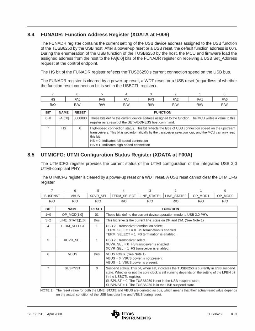
8−9SLLS535E − April 2008 TUSB6250
8.4 FUNADR: Function Address Register (XDATA at F009)
The FUNADR register contains the current setting of the USB device address assigned to the USB functionof the TUSB6250 by the USB host. After a power-up reset or a USB reset, the default function address is 00h.During the enumeration of the USB function of the TUSB6250 by the host, the MCU and firmware load theassigned address from the host to the FA[6:0] bits of the FUNADR register on receiving a USB Set_Addressrequest at the control endpoint.
The HS bit of the FUNADR register reflects the TUSB6250’s current connection speed on the USB bus.
The FUNADR register is cleared by a power-up reset, a WDT reset, or a USB reset (regardless of whetherthe function reset connection bit is set in the USBCTL register).
7 6 5 4 3 2 1 0
HS FA6 FA5 FA4 FA3 FA2 FA1 FA0
R/O R/W R/W R/W R/W R/W R/W R/W
BIT NAME RESET FUNCTION
6−0 FA[6:0] 0000000 These bits define the current device address assigned to the function. The MCU writes a value to thisregister as a result of the SET-ADDRESS host command.
7 HS 0 High-speed connection status. This bit reflects the type of USB connection speed on the upstreamtransceivers. This bit is set automatically by the transceiver selection logic and the MCU can only readthis bit.HS = 0 Indicates full-speed connectionHS = 1 Indicates high-speed connection
8.5 UTMICFG: UTMI Configuration Status Register (XDATA at F00A)
The UTMICFG register provides the current status of the UTMI configuration of the integrated USB 2.0UTMI-compliant PHY.
The UTMICFG register is cleared by a power-up reset or a WDT reset. A USB reset cannot clear the UTMICFGregister.
7 6 5 4 3 2 1 0
SUSPNST VBUS XCVR_SEL TERM_SELECT LINE_STATE1 LINE_STATE0 OP_MOD1 OP_MOD0
R/O R/O R/O R/O R/O R/O R/O R/O
BIT NAME RESET FUNCTION
1−0 OP_MOD[1:0] 01 These bits define the current device operation mode to USB 2.0 PHY.
3−2 LINE_STATE[1:0] Bus This bit reflects the current line_state on DP and DM. (See Note 1)
4 TERM_SELECT 1 USB 2.0 transceiver termination select.TERM_SELECT = 0 HS termination is enabled.TERM_SELECT = 1 FS termination is enabled.
5 XCVR_SEL 1 USB 2.0 transceiver select.XCVR_SEL = 0 HS transceiver is enabled.XCVR_SEL = 1 FS transceiver is enabled.
6 VBUS Bus VBUS status. (See Note 1)VBUS = 0 VBUS power is not present.VBUS = 1 VBUS power is present.
7 SUSPNST 0 Suspend status. This bit, when set, indicates the TUSB6250 is currently in USB suspendstate. Whether or not the core clock is still running depends on the setting of the LPEN bitin the USBCTL register.SUSPNST = 0 The TUSB6250 is not in the USB suspend state.SUSPNST = 1 The TUSB6250 is in the USB suspend state.
NOTE 1: The reset value for both the LINE_STATE and VBUS are denoted as bus, which means that their actual reset value dependson the actual condition of the USB bus data line and VBUS during reset.

8−10 SLLS535E − April 2008TUSB6250
8.6 USBFCL: USB Frame Counter Low-Byte Register (XDATA at F00B)
The USBFCL register contains the read-only USB frame counter low-byte value of the 11-bit frame numbervalue received from the USB host in the start-of-frame packet. The frame number bit values are updated bythe hardware for each USB frame with the frame number field value received in the USB start-of-frame packet.The frame number can be used as a time stamp by the USB function. If the frame number of the TUSB6250is not locked to the USB host frame timer, then the frame number is incremented from the previous value whena pseudo start-of-frame occurs.
The USBFCL register is cleared by a power-up reset or a WDT reset. A USB reset cannot clear the USBFCLregister.
7 6 5 4 3 2 1 0
FRAMNUM7 FRAMNUM6 FRAMNUM5 FRAMNUM4 FRAMNUM3 FRAMNUM2 FRAMNUM1 FRAMNUM0
R/O R/O R/O R/O R/O R/O R/O R/O
BIT NAME RESET FUNCTION
7−0 FRAMNUM[7:0] 00h These bits indicate the frame number lower-order 8-bit value.
8.7 USBFCH: USB Frame Counter High-Byte Register (XDATA at F00C)
The FRAMNUM[10:8] bits of the USBFCH register contain the read-only USB frame counter high-byte valueof the 11-bit frame number value received from the USB host in the start-of-frame packet. The UFRMNUM[2:0]bits contain the read-only micro frame number.
The USBFCH register is cleared by a power-up reset or a WDT reset. A USB reset cannot clear the USBFCHregister.
7 6 5 4 3 2 1 0
RSV RSV UFRAMNUM2 UFRAMNUM1 UFRAMNUM0 FRAMNUM10 FRAMNUM9 FRAMNUM8
R/O R/O R/O R/O R/O R/O R/O R/O
BIT NAME RESET FUNCTION
2−0 FRAMNUM[10:8] 000 These bits indicate the frame number higher-order 3-bit value.
5−3 UFRAMNUM[2:0] 000 These three bits indicate the microframe number.
7−6 RSV 00 Reserved. The application firmware must ensure these two bits are set to 00 during normaloperation.
8.8 USBWKUP: USB Wake-Up Reason Register (XDATA at F00D)
The USBWKUP register indicates the USB wakeup event reason (source) from the embedded MCU’s port-3GPIO pins and VBUS pin.
All four status-change bits (P34CHG, P35CHG, VBUSCHG, and CDCHG) in the USBWKUP register are setindividually by the hardware when their corresponding enable bit is set in the MCUCNFG register (at ESFRFCh), with the exception that VBUSCHG is always enabled. They can be cleared by the MCU writing a 1 tothe proper bit location (writing a 0 has no effect). In addition, the OR-result of these four status-change bits,when set, generates the WAKCLK interrupt if the interrupt is enabled in the USBMSK register (R/C notationindicates read and set-to-clear only by the MCU).
Any status-change bit, when set, indicates there is a status-change event that occurred since the last time theMCU cleared the same status-change bit. Below are important notes regarding the consecutive status-changeevents that occur before the MCU services and clears the current WAKCLK interrupt, assuming the relatedstatus-change event is enabled in the MCUCNFG register.
• As described in Section 8.3.2, WAKCLK Interrupt and Remote Wakeup, regardless if the newstatus-change event occurring is the same as the one that already occurred, consecutive status-change

8−11SLLS535E − April 2008 TUSB6250
events do not trigger a new WAKCLK interrupt if there is already a WAKCLK interrupt in the queue. Thisavoids the MCU being interrupted by too many WAKCLK interrupts.
• Following the same guideline, when consecutive status-change events happen:
− If the source of the new status-change event that occurred is different from the ones that alreadyoccurred, the new status-change event is logged in the corresponding status-change bit of theUSBWKUP register. For example, if the CDCHG bit is already set, but VBUSCHG bit is not set, a newVBUS status change causes the VBUSCHG bit to be set, although it might not trigger a new WAKCLKinterrupt if the current WAKCLK interrupt is still in the queue.
− If the source of the new status-change event occurred is the same as the ones that already occurred,the new status-change event is ignored. For example, if CDCHG bit is still set, but a new CDCHGevent is detected, the new CDCHG status-change event is ignored. This avoids unnecessarychanges in the status-change bits of the USBWKUP register caused by redundant status-changeevents.
• For detailed information regarding the WAKCLK interrupt, see Section 8.3.2, WAKCLK Interrupt andRemote Wakeup.
• Even if the WAKCLK interrupt is not enabled, the status-change events can still be observed by pollingthe MCUCNFG register, as long as the event detection is enabled in the MCUCNFG register.
The CD1STEN and CD2STEN bits in the MCUCNFG register can be individually enabled for separate wakeupevent detection. However, because these two bits share the same status-change indication bit (CDCHG) inthe USB wakeup reason register, clearing one interrupt source results in the interrupt source indication of theother being cleared at the same time.
To avoid missing status changes on the port-3 GPIO, especially in the suspend condition in which the clockmay be shut down, the following two sets of circuitries are used for generating the four status-change bits (bit7 to 4).
• Debounced status-change circuitry is used whenever the clock is available and stable. The debouncingtime interval is 1.28 ms, which means that only switching lasting longer than 1.28 ms is considered a validlogic transition on the related port-3 GPIO pin.
• Asynchronously triggered status-change circuitry is used to latch the change event when the remotewakeup is disabled and the low-power enable is true (LPEN bit in USBCTL is set), while the TUSB6250is in the suspend state.
Bits[3:0] provide the debounced read-only value of the current logic level on the corresponding GPIO pins ofport 3. The debouncing time interval is 1.28 ms.
The USBWKUP register is cleared by a power-up reset or a WDT reset. A USB reset cannot clear theUSBWKUP register.
7 6 5 4 3 2 1 0
P35CHG P34CHG VBUSCHG CDCHG P35ST P34ST CD2ST CD1ST
R/C R/C R/C R/C R/O R/O R/O R/O
BIT NAME RESET FUNCTION
0 CD1ST 1 Compact flash card/media detection CD1 status bit. This bit represents the debounced status valueon the CD1 pin.CD1ST = 1 CF card/media is not inserted.CD1ST = 0 CF card/media may be inserted (a firm insertion depends on the status on both media
detection pins).
1 CD2ST 1 Compact flash card/media detection CD2 status bit. This bit represents the debounced status valueon the CD2 pin.CD2ST = 1 CF card/media is not inserted.CD2ST = 0 CF card/media may be inserted (a firm insertion depends on the status on both media
detection pins).

8−12 SLLS535E − April 2008TUSB6250
BIT FUNCTIONRESETNAME
2 P34ST 0 P3.4 status bit. This bit represents the debounced status value on the P3.4 pin.
3 P35ST 0 P3.5 status bit. This bit represents the debounced status value on the P3.5 pin.
4 CDCHG 0 Compact flash card/media detection pin status-change bit. This bit, when set, indicates a statuschange occurred at either the CD1 or CD2 pin. The firmware must read the status of these two pinsto ensure a correct media insertion.CDCHG = 0 No CF card/media detection status change occurred.CDCHG = 1 CF card/media detection status change occurred on at least one CD pin.
5 VBUSCHG 0 VBUS status-change bit.VBUSCHG = 0 No VBUS status change occurred.VBUSCHG = 1 A VBUS status change occurred.
6 P34CHG 0 P34CHG status-change bit.P34CHG = 0 No P3.4 pin status change occurred.P34CHG = 1 A P3.4 pin status change occurred.
7 P35CHG 0 P35CHG status-change bit.P35CHG = 0 No P3.5 pin status change occurred.P35CHG = 1 A P3.5 pin status change occurred.
8.9 Endpoint-0 Descriptor Registers
All EDBs (endpoint descriptor block, including EDB-0 and EDB-1 to EDB-4) are implemented in registers.Their respective endpoint data buffers are implemented in SPRAM. Table 8−2 defines the registers and theirrespective address used for EDB-0.
EDB-0 has no base-address register, because these addresses are hardwired and depend on theconfiguration set by the BZ[1:0] bits in the IEPCNFG_0 register (see Table 8−3).
Table 8−2. Input/Output EDB-0 RegistersADDRESS REGISTER NAME DESCRIPTION
F004 OEPBCNX_0 Output endpoint_0: X-buffer byte-count register
F003 OEPCNFG_0 Output endpoint_0: configuration register
F001 IEPBCNX_0 Input endpoint_0: X-buffer byte-count register
F000 IEPCNFG_0 Input endpoint_0: configuration register
Table 8−3. Input/Output EDB-0 Buffer Location as Defined by BZ[1:0]
IN/OUT DBUF=0 BZ[1:0]=0 BZ[1:0]=1 BZ[1:0]=2 BZ[1:0]=3IN/OUTENDPOINT-0 SIZE (BYTES) = 8 16 32 64
InputEnd address E00F E01F E03F E07F
InputIEP0BA = E008 E010 E020 E040
OutputEnd address E007 E00F E01F E03F
OutputOEP0BA = E000 E000 E000 E000

8−13SLLS535E − April 2008 TUSB6250
8.9.1 IEPCNFG_0: Input Endpoint-0 Configuration Register (XDATA at F000)
The IEPCNFG_0 register contains various bits used to configure and control this endpoint.
7 6 5 4 3 2 1 0
UBME NAK_INTE TOGLE RSV STALL USBIE BZ1 BZ0R/W R/W R/O R/O R/W R/W R/W R/W
BIT NAME RESET FUNCTION
1−0 BZ[1:0] 00b Endpoint-0 buffer size for IN and OUT transaction. The value of this field also defines the starting addressof the input buffer. See Table 8−3.00 = 8 bytes01 = 16 bytes10 = 32 bytes11 = 64 bytes
2 USBIE 0 USB interrupt enable on transaction completion. Set/cleared by the MCU.USBIE = 0 No interruptUSBIE = 1 Interrupt on transaction completion
3 STALL 0 USB stall condition indication. Set/cleared by the MCU.STALL = 0 No stallSTALL = 1 USB stall condition. If set by the MCU, a STALL handshake is initiated and the bit is cleared
automatically by the next setup transaction.
4 RSV 0 Reserved
5 TOGLE 0 USB toggle bit. The hardware resets this bit when the setup packet is received.
6 NAK_INTE 0 NAK interrupt enableNAK_INTE = 0 NAK does not trigger interrupt.NAK_INTE = 1 NAK triggers an interrupt.
7 UBME 0 UBM enable/disable bit. Set/cleared by the MCU.UBME = 0 UBM cannot use this endpoint.UBME = 1 UBM can use this endpoint.
8.9.2 IEPBCN_0: Input Endpoint-0 Buffer Byte-Count Register (XDATA at F001)
The IEPBCN_0 register contains the NAK bit and the 7-bit value used to specify the amount of data to betransmitted in a data packet to the USB host.
7 6 5 4 3 2 1 0
NAK C6 C5 C4 C3 C2 C1 C0
R/W R/W R/W R/W R/W R/W R/W R/W
BIT NAME RESET FUNCTION
6−0 C[6:0] 0000000 Byte count. Only count of 0 to 64 (00h to 40h) is supported.00h Byte count = 0:40h Byte count = 6441h to 7Fh should not be used. If the MCU writes any value greater than 0x40 to C[6:0], the TUSB6250hardware corrects it and only writes 0x40 to C[6:0].
7 NAK 1 NAK=0 Buffer contains a valid packet for Host-IN request.NAK=1 Buffer is empty (TUSB6250 NAKs the host-IN request).
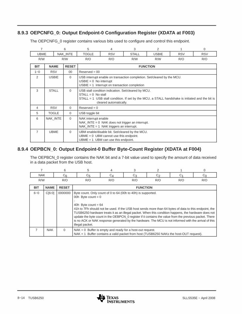
8−14 SLLS535E − April 2008TUSB6250
8.9.3 OEPCNFG_0: Output Endpoint-0 Configuration Register (XDATA at F003)
The OEPCNFG_0 register contains various bits used to configure and control this endpoint.
7 6 5 4 3 2 1 0
UBME NAK_INTE TOGLE RSV STALL USBIE RSV RSV
R/W R/W R/O R/O R/W R/W R/O R/O
BIT NAME RESET FUNCTION
1−0 RSV 00 Reserved = 00
2 USBIE 0 USB interrupt enable on transaction completion. Set/cleared by the MCU.USBIE = 0 No interruptUSBIE = 1 Interrupt on transaction completion
3 STALL 0 USB stall condition indication. Set/cleared by MCU.STALL = 0 No stallSTALL = 1 USB stall condition. If set by the MCU, a STALL handshake is initiated and the bit is
cleared automatically.
4 RSV 0 Reserved = 0
5 TOGLE 0 USB toggle bit
6 NAK_INTE 0 NAK interrupt enableNAK_INTE = 0 NAK does not trigger an interrupt.NAK_INTE = 1 NAK triggers an interrupt.
7 UBME 0 UBM enable/disable bit. Set/cleared by the MCU.UBME = 0 UBM cannot use this endpoint.UBME = 1 UBM can use this endpoint.
8.9.4 OEPBCN_0: Output Endpoint-0 Buffer Byte-Count Register (XDATA at F004)
The OEPBCN_0 register contains the NAK bit and a 7-bit value used to specify the amount of data receivedin a data packet from the USB host.
7 6 5 4 3 2 1 0
NAK C6 C5 C4 C3 C2 C1 C0R/W R/O R/O R/O R/O R/O R/O R/O
BIT NAME RESET FUNCTION
6−0 C[6:0] 0000000 Byte count. Only count of 0 to 64 (00h to 40h) is supported.00h Byte count = 0:40h Byte count = 6441h to 7Fh should not be used. If the USB host sends more than 64 bytes of data to this endpoint, theTUSB6250 hardware treats it as an illegal packet. When this condition happens, the hardware does notupdate the byte count in the OEBPCN_0 register if it contains the value from the previous packet. Thereis no ACK or NAK response generated by the hardware. The MCU is not informed with the arrival of thisillegal packet.
7 NAK 0 NAK = 0 Buffer is empty and ready for a host-out request.NAK = 1 Buffer contains a valid packet from host (TUSB6250 NAKs the host-OUT request).

8−15SLLS535E − April 2008 TUSB6250
Table 8−4 shows the buffer location address map for a single buffer with a buffer size of 64 bytes.
Table 8−4. EDB0 Buffer Locations (in SPRAM)ADDRESS NAME DESCRIPTION
EFFF TOPBUFF Top of buffer space
↑|||||↓
TOPBUFF
Buffer space4K – 128 bytes free
E080
E07F ↑
↑|↓
64 bytesI
Input endpoint_0, bufferI
E040 ↓
E03F ↑↑|↓
64 bytes
↑I
Output endpoint_0, buffer|
E000
|↓
NOTE: This table is based on a single buffer with a buffer size of 64 bytesfor both input and output endpoint-0.
8.10 Endpoint Descriptor Block (EDB-1 to EDB-4)
The endpoint descriptor block (EDB) defines the endpoint characteristics for data transfer between the USBand the UBM. Four input and four output endpoints are provided. All EDBs are implemented inmemory-mapped registers as defined in Table 6−2.
Double data buffers are provided for EDB-1 to EDB-4 (both input and output endpoints). The firmware in theMCU decides whether to use the double data buffers by writing to the DBUF bit in the IEPCNFG_n andOEPCNFG_n registers. The double data buffer is disabled by default (DBUF = 0). In this case, only the primarydata buffer (X-buffer) is enabled.
Each EDB contains information describing the X and Y-buffers. In addition, it provides general statusinformation. Figure 8−2 and Figure 8−3 illustrate how the IN_Endpoint_number (E[2:0]) andOUT_Endpoint_number (E[2:0]) are used to generate the index (address) to the input EDB and the outputEDB, respectively, in the MMR memory map. Note that A[3] is used to distinguish between input and output.
Table 8−5 illustrates each EDB entry (register) for EDB-1 to EDB-4.
Figure 8−4 illustrates how the complete 16-bit EDB-buffer base address within the MMR memory map isgenerated in the TUSB6250 hardware for each EDB data buffer.
As defined in the USB 2.0 specification, the maximum packet size is 512 bytes for a high-speed bulk endpointand 64 bytes for a full-speed bulk endpoint.
Endpoint # IN
Bit Value 1 1 1 1 0 0 0 0 0 E2 E1 E0 0 0 0 0
Bit Number A15 A14 A13 A12 A11 A10 A9 A8 A7 A6 A5 A4 A3 A2 A1 A0
Figure 8−2. IN-Endpoint Index Generation

8−16 SLLS535E − April 2008TUSB6250
Endpoint # OUT
Bit Value 1 1 1 1 0 0 0 0 0 E2 E1 E0 1 0 0 0
Bit Number A15 A14 A13 A12 A11 A10 A9 A8 A7 A6 A5 A4 A3 A2 A1 A0
Figure 8−3. OUT-Endpoint Index Generation
Table 8−5. EDB Entries in MMR (n = 1 to 4)OFFSET
(see Note 2) ENTRY NAME DESCRIPTION
07 EPBCNHY_n I/O endpoint_n: Y byte-count (HB) register
06 EPBCNLY_n I/O endpoint_n: Y byte-count (LB) register
05 EPBBADRY_n I/O endpoint_n: Y-buffer base address register (see Note 1)
04 EPSIZXY_n I/O endpoint_n: X/Y-buffer size register
03 EPBCNHX_n I/O endpoint_n: X byte-count (HB) register
02 EPBCNLX_n I/O endpoint_n: X byte-count (LB) register
01 EPBBADRX_n I/O endpoint_n: X-buffer base address register (see Note 1)
00 EPCNFG_n I/O endpoint_n: configuration register
NOTES: 1. The entry contains the A[11:4] portion of a 16-bit address. See Figure 8−4.2. Offset number is based on the A[2:0] value.
Inserted by Hardware Base Address in EDB Inserted by Hardware
Bit Value 1 1 1 0 A11 A10 A9 A8 A7 A6 A5 A4 0 0 0 0
Bit Number 15 14 13 12 11 10 9 8 7 6 5 4 3 2 1 0
Figure 8−4. 16-Bit EDB Data Buffer Address Generation From the Value of the Buffer Base Address
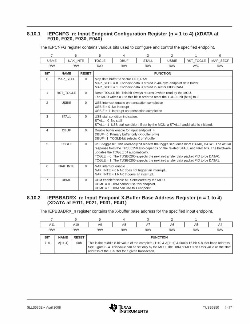
8−17SLLS535E − April 2008 TUSB6250
8.10.1 IEPCNFG_n: Input Endpoint Configuration Register (n = 1 to 4) (XDATA atF010, F020, F030, F040)
The IEPCNFG register contains various bits used to configure and control the specified endpoint.
7 6 5 4 3 2 1 0
UBME NAK_INTE TOGLE DBUF STALL USBIE RST_TOGLE MAP_SECF
R/W R/W R/O R/W R/W R/W W/O R/W
BIT NAME RESET FUNCTION
0 MAP_SECF 0 Map data buffer to sector FIFO RAM.MAP_SECF = 0 Endpoint data is stored in 4K-byte endpoint data buffer.MAP_SECF = 1 Endpoint data is stored in sector FIFO RAM.
1 RST_TOGLE 0 Reset TOGLE bit. This bit always returns 0 when read by the MCU.The MCU writes a 1 to this bit in order to reset the TOGLE bit (bit 5) to 0.
2 USBIE 0 USB interrupt enable on transaction completionUSBIE = 0 No interruptUSBIE = 1 Interrupt on transaction completion
3 STALL 0 USB stall condition indication.STALL= 0 No stallSTALL= 1 USB stall condition. If set by the MCU, a STALL handshake is initiated.
4 DBUF 0 Double buffer enable for input endpoint_n.DBUF= 0 Primary buffer only (X-buffer only)DBUF= 1 TOGLE-bit selects X or Y-buffer
5 TOGLE 0 USB toggle bit. This read-only bit reflects the toggle sequence bit of DATA0, DATA1. The actualresponse from the TUSB6250 also depends on the related STALL and NAK bits. The hardwareupdates the TOGLE bit automatically.TOGLE = 0 The TUSB6205 expects the next in-transfer data packet PID to be DATA0.TOGLE = 1 The TUSB6205 expects the next in-transfer data packet PID to be DATA1.
6 NAK_INTE 0 NAK interrupt enableNAK_INTE = 0 NAK does not trigger an interrupt.NAK_INTE = 1 NAK triggers an interrupt.
7 UBME 0 UBM enable/disable bit. Set/cleared by the MCU.UBME = 0 UBM cannot use this endpoint.UBME = 1 UBM can use this endpoint
8.10.2 IEPBBADRX_n: Input Endpoint X-Buffer Base Address Register (n = 1 to 4)(XDATA at F011, F021, F031, F041)
The IEPBBADRX_n register contains the X-buffer base address for the specified input endpoint.
7 6 5 4 3 2 1 0
A11 A10 A9 A8 A7 A6 A5 A4
R/W R/W R/W R/W R/W R/W R/W R/W
BIT NAME RESET FUNCTION
7−0 A[11:4] 00h This is the middle 8-bit value of the complete (1110 & A[11:4] & 0000) 16-bit X-buffer base address.See Figure 8−4. This value can be set only by the MCU. The UBM or MCU uses this value as the startaddress of the X-buffer for a given transaction.

8−18 SLLS535E − April 2008TUSB6250
8.10.3 IEPBCNLX_n: Input Endpoint X-Buffer Byte-Count Low-Byte Register (n = 1to 4) (XDATA at F012, F022, F032, F042)
The IEPBCNLX_n register contains the lower 8-bit value in the X-buffer that is used to specify the amount ofdata to be transmitted in a data packet to the USB host.
7 6 5 4 3 2 1 0
C7 C6 C5 C4 C3 C2 C1 C0
R/W R/W R/W R/W R/W R/W R/W R/W
BIT NAME RESET FUNCTION
7−0 C[7:0] 00h X-buffer byte-count: low byte
8.10.4 IEPBCNHX_n: Input Endpoint X-Buffer Byte-Count High-Byte Register (n = 1 to4) (XDATA at F013, F023, F033, F043)
The IEPBCNHX_n register contains the NAK bit and the higher 3-bit value in the X-buffer that is used to specifythe amount of data to be transmitted in a data packet to the USB host.
7 6 5 4 3 2 1 0
NAK RSV RSV RSV RSV C10 C9 C8
R/W R/O R/O R/O R/O R/W R/W R/W
BIT NAME RESET FUNCTION
2−0 C[10:8] 0 X-buffer byte count higher 3 bits. These bits in combination with C[7:0] provide the byte count of a giventransaction (count = 0 to 2047).
6−3 RSV 0 Reserved = 0
7 NAK 0 NAK bit is used as flow control handshake for X-buffer.NAK = 0 This bit is cleared to 0 by the firmware to indicate that the endpoint data buffer contains a
valid packet for Host-IN request.NAK = 1 This bit is set to 1 by the TUSB6250 hardware to indicate that the endpoint data buffer is empty
(TUSB6250 NAKs the Host-IN request).
Following is the procedure to be used by the firmware when using the NAK bit for flow-control handshake. Forthe purpose of illustration, it is assumed that the double buffer (DBUF) is enabled. If DBUF is not enabled, theX-buffer is always used regardless of the value of the data packet PID of the coming in-transfer.
1. The first in-transfer comes when the in-endpoint buffer is empty (data payload not ready for the in-transferreceived) and NAK =1. The TUSB6250 responds to the in-transfer with a NAK handshake and startspreparing the data payload required for this in-transfer.
2. The MCU is alerted with a NAK interrupt to the current in-endpoint. The firmware loads the data into eitherthe X-buffer or Y-buffer depending on the following conditions:
− If DBUF = 1, TOGLE = 0, and the data PID = DATA0:
The firmware loads the data into the X-buffer of the endpoint data buffer (4K bytes EDB) and updatesthe X-buffer byte-count information in IEPBCNLX_n and IEPBCNHX_n registers.
− If DBUF = 1, TOGLE = 1 and the data PID = DATA1:
The firmware loads the data into the Y-buffer of the endpoint data buffer (4K byte EDB) and updatesthe Y-buffer byte-count information in the IEPBCNLY_n and IEPBCNHY_n registers.
3. The firmware then clears the NAK bit to 0 to indicate to the TUSB6250 hardware that a valid data packetwith the specified byte count is ready to be transmitted to the USB host.
4. The TUSB6250 hardware sends the data packet in the specified length on the USB host sending the nextIN-request with a valid IN-token.

8−19SLLS535E − April 2008 TUSB6250
5. Once the USB host acknowledges the host-IN transfer with an ACK, the TUSB6250 hardware sets theNAK bit to 1, so that any new host-IN request is NAKed until the MCU and firmware get the new requireddata payload ready.
8.10.5 IEPSIZXY_n: Input Endpoint X/Y-Buffer Size Register (n = 1 to 4) (XDATA atF014, F024, F034, F044)
The IEPSIZXY register contains the X- and Y-buffer size for the specified input endpoint.
7 6 5 4 3 2 1 0
S10 S9 S8 S7 S6 S5 S4 S3
R/W R/W R/W R/W R/W R/W R/W R/W
BIT NAME RESET FUNCTION
7−0 S[10:3] 00h X- and Y-buffer size in byte: S[2:0] is padded with zeros (S[10:3] & 000) to produce an 11-bit value.Size is 0 to 1024 in increments of eight.
8.10.6 IEPBBADRY_n: Input Endpoint Y-Buffer Base Address Register (n = 1 to 4)(XDATA at F015, F025, F035, F045)
The IEPBBADRY_n register contains the Y-buffer base address for the specified input endpoint.
7 6 5 4 3 2 1 0
A11 A10 A9 A8 A7 A6 A5 A4
R/W R/W R/W R/W R/W R/W R/W R/W
BIT NAME RESET FUNCTION
7−0 A[11:4] 00h This is the middle 8-bit value of the complete (1110 & A[11:4] & 0000) 16-bit Y-buffer base address.See Figure 8−4. This value is set by the MCU. The UBM or the MCU uses this value as the startaddress of the Y-buffer for a given transaction.
8.10.7 IEPBCNLY_n: Input Endpoint Y-Buffer Byte-Count Low-Byte Register (n = 1 to4) (XDATA at F016, F026, F036, F046)
The IEPBCNLY_n register contains the lower 8-bit value in the Y-buffer that is used to specify the amount ofdata to be transmitted in a data packet to the USB host.
7 6 5 4 3 2 1 0
C7 C6 C5 C4 C3 C2 C1 C0
R/W R/W R/W R/W R/W R/W R/W R/W
BIT NAME RESET FUNCTION
7−0 C[7:0] 00h Y-buffer byte-count: low byte

8−20 SLLS535E − April 2008TUSB6250
8.10.8 IEPBCNHY_n: Input Endpoint Y-Buffer Byte-Count High-Byte Register (n = 1to 4) (XDATA at F017, F027, F037, F047)
The IEPBCNHY_n register contains the NAK bit and the higher 3-bit value in the Y-buffer that is used to specifythe amount of data to be transmitted in a data packet to the USB host. See the procedure described in theIEPBCNHX_n register when using the NAK bit for flow control handshake.
7 6 5 4 3 2 1 0
NAK RSV RSV RSV RSV C10 C9 C8
R/W R/O R/O R/O R/O R/W R/W R/W
BIT NAME RESET FUNCTION
2−0 C[10:8] 000 Y-buffer byte count higher 3 bits. These bits, in combination with C[7:0], provide the byte count of agiven transaction (count = 0 to 2047).
6−3 RSV 0000 Reserved = 0
7 NAK 0 NAK bit is used as flow control handshake for Y-buffer.NAK = 0 Buffer contains a valid packet for the Host-IN request.NAK = 1 Buffer is empty (TUSB6250 NAKs the host-IN request).
8.10.9 OEPCNF_n: Output Endpoint Configuration Register (n = 1 to 4) (XDATA atF018, F028, F038, F048)
The OEPCNF_n register contains various bits used to configure and control the specified endpoint.
7 6 5 4 3 2 1 0
UBME NAK_INTE TOGLE DBUF STALL USBIE RS_TOGLE MAP_SECF
R/W R/W R/O R/W R/W R/W W/O R/W
BIT NAME RESET FUNCTION
0 MAP_SECF 0 Map data buffer to sector FIFO RAM. The MCU writes to this bit to inform the state machinewhether it wants the data to be transferred/stored in either the 4K-byte EDB buffer or the sectorFIFO. If the sector FIFO is selected, when the data transfer phase is over, the state machineautomatically switches the data storage area back to the 4K-byte EDB buffer.MAP_SECF = 0 Endpoint data is stored in the 4K-byte endpoint data buffer.MAP_SECF = 1 Endpoint data is stored in the sector FIFO RAM.
1 RST_TOGLE 0 Reset TOGLE. This bit always returns 0 when read by the MCU.The MCU can write a 1 to this bit in order to reset the TOGLE bit (bit 5) to ‘0’.
2 USBIE 0 USB interrupt enable on transaction completion. Set/cleared by the MCU.USBIE = 0 No interruptUSBIE = 1 Interrupt on transaction completion
3 STALL 0 USB stall condition indication.STALL = 0 No stallSTALL = 1 USB stall condition. If set by the MCU, a STALL handshake is initiated.
4 DBUF 0 Double buffer enable for output endpoint_n.DBUF = 0 Primary buffer only (X-buffer only)DBUF = 1 TOGLE-bit selects X- or Y-buffer.
5 TOGLE 0 USB toggle bit. This read-only bit reflects the toggle sequence bit of DATA0, DATA1. The actualresponse from the TUSB6250 depends on the related STALL and NAK bits. The hardwareupdates the TOGLE bit automatically.TOGLE = 0 The TUSB6250 expects the next out-transfer data packet PID to be DATA0.TOGLE = 1 The TUSB6250 expects the next out-transfer data packet PID to be DATA1.
6 NAK_INTE 0 NAK interrupt enableNAK_INTE = 0 NAK does not trigger an interrupt.NAK_INTE = 1 NAK triggers an interrupt.
7 UBME 0 UBM enable/disable bit. Set/cleared by the MCU.UBME = 0 UBM cannot use this endpoint.UBME = 1 UBM can use this endpoint.

8−21SLLS535E − April 2008 TUSB6250
8.10.10 OEPBBAX_n: Output Endpoint X-Buffer Base Address Register (n = 1 to 4) (XDATA at F019,F029, F039, F049)
The OEPBBAX_n register contains the X-buffer base address for the specified output endpoint.
7 6 5 4 3 2 1 0
A11 A10 A9 A8 A7 A6 A5 A4
R/W R/W R/W R/W R/W R/W R/W R/W
BIT NAME RESET FUNCTION
7−0 A[11:4] 00h This is the middle 8-bit value of the complete (1110 and A[11:4] and 0000) 16-bit X-buffer base address.See Figure 8−4. This value is set by the MCU. The UBM or the DMA uses this value as the startaddress of X-buffer for a given transaction.
8.10.11 OEPBCNLX_n: Output Endpoint X-Buffer Byte-Count Low-Byte Register (n = 1 to 4) (XDATA atF01A, F02A, F03A, F04A)
The OEPBCNLX_n register contains the lower 8-bit value in the X-buffer that is used to specify the amountof data received in a data packet from the USB host.
7 6 5 4 3 2 1 0
C7 C6 C5 C4 C3 C2 C1 C0
R/O R/O R/O R/O R/O R/O R/O R/O
BIT NAME RESET FUNCTION
7−0 C[7:0] 00h X-buffer byte-count: low byte
8.10.12 OEPBCNHX_n: Output Endpoint X-Buffer Byte-Count High-Byte Register (n = 1 to 4) (XDATA atF01B, F02B, F03B, F04B)
The OEPBCNHX_n register contains the NAK bit and the higher 3-bit value in the X-buffer that is used tospecify the amount of data received in a data packet from the USB host.
7 6 5 4 3 2 1 0
NAK RSV RSV RSV RSV C10 C9 C8R/W R/O R/O R/O R/O R/O R/O R/O
BIT NAME RESET FUNCTION
2−0 C[10:8] 000 X-buffer byte count higher 3 bits. These bits, in combination with C[7:0], provide the byte count of agiven transaction (count = 0 to 2047).
6−3 RSV 0000 Reserved = 0
7 NAK 0 NAK bit is used as flow control handshake for X-buffer.NAK = 0 This bit is cleared to 0 by the firmware to indicate that the endpoint data buffer is empty and
ready for a Host-OUT request.NAK = 1 This bit is set to 1 by the TUSB6250 hardware to indicate that the endpoint data buffer
contains a valid packet from the host (TUSB6250 NAKs the host-OUT request).
Below is the procedure to be followed by the firmware when using the NAK bit for flow control handshake. Forthe purpose of illustration, it is assumed that the double buffer (DBUF) is enabled. If DBUF is not enabled, theX-buffer is always used regardless of the value of the data packet PID of the coming out-transfer.
• Assume that NAK = 0 and both out-endpoint data buffers are empty, when the first out-transfer comes.The TUSB6250 responds to the out-transfer with an ACK handshake and starts processing the datapayload received for this out-transfer immediately.
• Meanwhile, the TUSB6250 hardware sets the NAK bit to 1 to indicate that the current endpoint data buffercontains a valid packet from the host such that the TUSB6250 can either NYET-then-NAK (for USBhigh-speed connection) or simply ACK-then-NAK (for USB full-speed connection) any further host-outrequest to this endpoint. It should be noted that both the X-buffer and Y-buffer have their own NAK bit.

8−22 SLLS535E − April 2008TUSB6250
• The UBM (USB buffer manager, a DMA engine on the USB side) of the TUSB6250 loads the data intoeither the X-buffer or Y-buffer, depending on the following conditions:
− If DBUF = 1, TOGLE = 0, and the data PID = DATA0:
The UBM loads the data into the X-buffer of the out-endpoint data buffer (4K-byte EDB) and updatesthe X-buffer byte-count information in the OEPBCNLX_n and OEPBCNHX_n registers.
− If DBUF = 1, TOGLE = 1, and the data PID = DATA1:
The UBM loads the data into the Y-buffer of the out-endpoint data buffer (4K-byte EDB) and updatesthe Y-buffer byte-count information in the OEPBCNLY_n and OEPBCNHY_n registers.
• The MCU is alerted with an ACK interrupt to the current out-endpoint. The firmware processes thereceived data packet stored in either the X-buffer or Y-buffer of the out-endpoint data buffers.
• Once the firmware finishes the processing, the out-endpoint data buffer is empty. The firmware then clearsthe NAK bit to 0 to indicate to the TUSB6250 hardware that it is ready for the next host-out request.
8.10.13 OEPSIZXY_n: Output Endpoint X/Y-Buffer Size Register (n = 1 to 4) (XDATA at F01C, F02C,F03C, F04C)
The OEPSIZXY_n register contains the X- and Y-buffer size for the specified output endpoint.
7 6 5 4 3 2 1 0
S10 S9 S8 S7 S6 S5 S4 S3
R/W R/W R/W R/W R/W R/W R/W R/W
BIT NAME RESET FUNCTION
7−0 S[10:3] 00h X- and Y-buffer size in bytes: S[10:3] is padded with zeros (S[10:3] & 000) to produce an 11-bit value.Size is 0 to 1024 in increments of eight.
8.10.14 OEPBBADRY_n: Output Endpoint Y-Buffer Base Address Register (n = 1 to 4) (XDATA at F01D,F02D, F03D, F04D)
The OEPBBADRY_n register contains the Y-buffer base address for the specified output endpoint.
7 6 5 4 3 2 1 0
A11 A10 A9 A8 A7 A6 A5 A4
R/W R/W R/W R/W R/W R/W R/W R/W
BIT NAME RESET FUNCTION
7−0 A[11:4] 00h This is the middle 8-bit value of the complete (1110 & A[11:4] & 0000) 16-bit Y-buffer base address.See Figure 8−4. This value can be set only by the MCU. The UBM or the MCU uses this value as thestart address of Y-buffer for a given transaction.
8.10.15 OEPBCNLY_n: Output Endpoint Y-Buffer Byte-Count Low-Byte Register (n = 1 to 4) (XDATA atF01E, F02E, F03E, F04E)
The OEPBCNLY_n register contains the lower 8-bit value in the Y-buffer that is used to specify the amountof data received in a data packet from the USB host.
7 6 5 4 3 2 1 0
C7 C6 C5 C4 C3 C2 C1 C0
R/O R/O R/O R/O R/O R/O R/O R/O
BIT NAME RESET FUNCTION
7−0 C[7:0] 00h Y-buffer byte-count: low byte

8−23SLLS535E − April 2008 TUSB6250
8.10.16 OEPBCNHY_n: Output Endpoint Y-Buffer Byte-Count High-Byte Register (n = 1 to 4) (XDATA atF01F, F02F, F03F, F04F)
The OEPBCNHY_n register contains the NAK bit and the higher 3-bit value in the Y-buffer that is used tospecify the amount of data received in a data packet from the USB host. See the procedure described in theOEPBCNHX_n register when using the NAK bit for flow control handshake.
7 6 5 4 3 2 1 0
NAK RSV RSV RSV RSV C10 C9 C8
R/W R/O R/O R/O R/O R/O R/O R/O
BIT NAME RESET FUNCTION
2−0 C[10:8] 000 Y-buffer byte count higher 3 bits. These bits, in combination with C[7:0], provide the byte count of agiven transaction (count = 0 to 2047).
6−3 RSV 0000 Reserved = 0
7 NAK 0 NAK bit is used as flow control handshake for the Y-buffer.NAK = 0 Buffer is empty and ready for a Host-OUT request.NAK = 1 Buffer contains a valid packet from the host (TUSB6250 NAKs the Host-OUT request)
8.11 Serial Number RegistersThe USB 2.0 specification encourages end-product vendors to support the unique USB device serial number.The USB Mass Storage Cass—Bulk Only Transport specification also requires that the serial number shallcontain at least 12 valid digits, represented as a UNICODE string and the last 12 digits of the serial numbershall be unique to each USB idVendor and idProduct pair.
The TUSB6250 supports the unique USB device serial numbers. The serial numbers can be either specifiedby the end-product developer in the header block of the external I2C EEPROM with the custom format orgenerated automatically by the TUSB6250 from its 48-bit on-chip unique die ID number.
Each TUSB6250 chip has a unique 48-bit serial die ID number, which is generated during the semiconductormanufacturing process. The die IDs may not increment sequentially; however, it is assured that any particular48-bit die ID will not be repeated during production for at least 9 years.
The following procedure is performed by the TUSB6250 to identify and report the required serial number backto the USB host:
• After a power-up reset, the boot code performs a read to the SERNUM0 to SERNUM5 registers andinitializes its device serial number variable field stored in the XDATA memory space with the read valuefrom these registers.
• The boot code then checks if the external I2C EEPROM is present on the I2C interface of the TUSB6250.If the EEPROM is present and contains a valid device serial number as part of the USB device descriptorinformation stored in the EEPROM, the boot code overwrites the serial number value stored in the XDATAmemory space with the one found in the EEPROM. Otherwise, the TUSB6250 serial number value storedin the XDATA memory space stays unchanged from the previous step.
• In summary:
− The serial number value specified in the external EEPROM has the highest priority to be loaded intothe XDATA memory space, which is used as part of the valid device descriptor information to bereported back to the USB host during USB device enumeration.
− When responding to the Get_DeviceDescriptor command from the USB host, if the external I2CEEPROM does not contain the valid serial number, the TUSB6250 converts the 48-bit unique serialnumber stored in the serial number registers into a string of 12 UNICODE characters and returns thestring to the host.
For detailed information regarding how to specify the custom serial number in the header block of the externalI2C EEPROM, see the TUSB6250 Boot Code application note (SLLA126).
Little-endian is used when describing the serial number registers with SERNUM0 as the least significant byte.

8−24 SLLS535E − April 2008TUSB6250
8.11.1 SERNUMn: Device Serial Number Register (Byte n, n = 0 to 5) (XDATA at F080 to F085)
After a power-up reset, the SERNUMn read-only register (SERNUMn) contains byte n of the complete 48-bitdevice serial number from the on-chip serial die ID number. A USB reset cannot reset the SERNUMn register.
7 6 5 4 3 2 1 0
D7 D6 D5 D4 D3 D2 D1 D0
R/O R/O R/O R/O R/O R/O R/O R/O
BIT NAME RESET FUNCTION
7−0 D[7:0] Device serial number byte n value Device serial number byte n value

Miscellaneous and GPIO Configuration Registers
9−1SLLS535E − April 2008 TUSB6250
9 Miscellaneous and GPIO Configuration RegistersThe TUSB6250 offers up to 13 GPIOs and three additional general-purpose open-drain outputs that can beused for an end-product-specific function. All the GPIOs and general-purpose open-drain outputs are mappedto port 2 and port 3 of the embedded MCU. Table 9−1 illustrates the TUSB6250 GPIO port mapping for theembedded MCU and some recommended usage.
Table 9−1. TUSB6250 Controller MCU GPIO Port MappingEMBEDDED MCU
PORT 3 AND PORT 2GPIO
TUSB6250PIN MAPPING RECOMMENDED PIN USAGE/FUNCTION
Port 3[0] P3.0/SIN SIN (serial in of the 8051 built-in serial port) or GPIO
Port 3[1] P3.1/SOUT SOUT (serial out of the 8051 built-in serial port) or GPIO
Port 3[2] P3.2/CD1 Remote-wakeup-capable GPIO can be used as a compact flash card insertion detect signal.
Port 3[3] P3.3/CD2 Remote-wakeup-capable GPIO can be used as a compact flash card insertion detect signal.
Port 3[4] P3.4 Remote-wakeup-capable GPIO
Port 3[5] P3.5 Remote-wakeup-capable GPIO
Port 3[6] P3.6 GPIO or ATA/ATAPI passed diagnostic/cable identifier (not implemented in hardware)
Port 3[7] P3.7 GPIO or ATA/ATAPI device active/device-1 present (not implemented in hardware)
Port 2[0] P2.0 GPIO
Port 2[1] P2.1/PWR100 General-purpose open-drain output for power-control purposes
Port 2[2] P2.2/PWR500 General-purpose open-drain output for power-control purposes (not implemented inhardware)
Port 2[3] P2.3 General-purpose open-drain output
Port 2[4] P2.4 GPIO
Port 2[5] P2.5 GPIO
Port 2[6] P2.6 GPIO
Port 2[7] P2.7 GPIO
The GPIO pins of this controller have integrated pullup and/or pulldown resistors. As described in the followingsections, these pullup and/or pulldown resistors can be easily configured by the MCU using the related pullupand pulldown configuration registers to meet the need for a broad range of applications.
The pullup resistor, if enabled, is connected between the GPIO pin and the DVDD power supply. The pulldownresistor, if enabled, is connected between the GPIO pin and ground.
There are some important notes regarding the port-2 and port-3 GPIOs of this controller:• All the port-2 GPIO pins, except P2.7, are 5-V fail-safe. P2.7 is a standard 3.3-V LVCMOS GPIO with only
a pullup resistor integrated internally.• All the port-3 GPIO pins, except P3.0 and P3.1, are 5-V fail-safe. P3.0 and P3.1 are standard 3.3-V
LVCMOS GPIOs with only a pullup resistor integrated internally.• Developers must pay special attention to a standard 8051 microcontroller feature, that is, the output buffer
of a GPIO pin only actively drives one MCU clock cycle for a 0-to-1 transition on the data bit of any GPIOport (internally connected to the input of the GPIO output buffer). The GPIO pin then floats to allow theweak pullup to maintain the logic-1 state.
• Based on the above standard 8051 behavior, the firmware and board level developers must ensure thatno pulldown resistor is enabled, either internal or external on the GPIO pin, if its output buffer is used tooutput a logic 1 state, otherwise, the pulldown discharges the logic-1 value on the GPIO pin. In otherwords, the pullup must be enabled by the firmware whenever the output buffer is used to output a logic-1state for any GPIO.
• If a GPIO is configured as input-only, the firmware can select either a pullup or pulldown resistor to beenabled for that GPIO pin.

Miscellaneous and GPIO Configuration Registers
9−2 SLLS535E − April 2008TUSB6250
• Following the standard 8051 convention, both port 2 and port 3 are bit addressable, which implies thatwithin the same GPIO port, some pins can be configured as inputs and others as outputs.
9.1 MODECNFG: Mode Configuration Register (XDATA at F088)
The MODECNFG register contains several parameters the MCU can use to configure the code and data RAMpartition, polarity of the INTRQ pin, and code RAM write access enable.
The MODECNFG register is cleared by a power-up reset or a WDT reset only. A USB reset cannot clear theMODECNFG register.
7 6 5 4 3 2 1 0
RSV RSV RSV RSV INTRQPOLR RAMPARTN1 RAMPARTN0 RAMWR_DIS
R/O R/O R/O R/O R/W R/W R/W R/W
BIT NAME RESET FUNCTION
0 RAMWR_DIS 0
Disables/enables the MCU write to the complete space of the code RAM with the space definedby RAMPARTN[1:0] bits.
RAMWR_DIS = 0 Allows the MCU write to the code RAM.
RAMWR_DIS = 1 Disables the MCU write to the code RAM.
2−1 RAMPARTN[1:0]
00 Code/data RAM partition setting bits. These bits are used by the MCU to change the defaultpartition of the 40K bytes of RAM to the other two supported code/sector FIFO memoryconfigurations. The TUSB6250 allows the maximum code size to be 32K bytes.
RAMPARTN[1:0] = 00 40K bytes of RAM is partitioned to be 32K bytes code and 8K bytes sectorFIFO (default).
RAMPARTN[1:0] = 01 40K bytes of RAM is partitioned to be 16K bytes code and 24K bytessector FIFO.
RAMPARTN[1:0] = 10 40K bytes of RAM is partitioned to be 8K bytes code and 32K bytes sectorFIFO.
RAMPARTN[1:0] = 11 Reserved
3 INTRQPOLR 0 TUSB6250 INTRQ pin polarity configuration by the MCU.
INTRQPOLR = 0 INTRQ is active-high (default setting as defined in the ATA/ATAPIspecification).
INTRQPOLR = 1 INTRQ is active-low.
7−4 RSV 0h Reserved
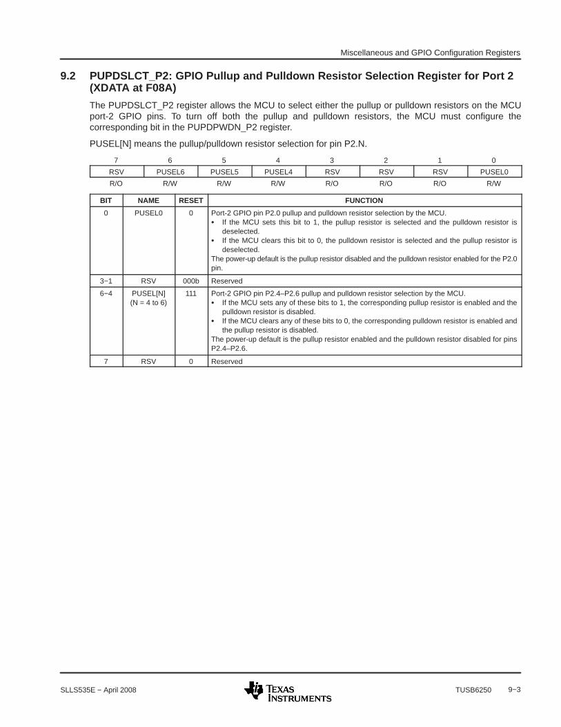
Miscellaneous and GPIO Configuration Registers
9−3SLLS535E − April 2008 TUSB6250
9.2 PUPDSLCT_P2: GPIO Pullup and Pulldown Resistor Selection Register for Port 2(XDATA at F08A)
The PUPDSLCT_P2 register allows the MCU to select either the pullup or pulldown resistors on the MCUport-2 GPIO pins. To turn off both the pullup and pulldown resistors, the MCU must configure thecorresponding bit in the PUPDPWDN_P2 register.
PUSEL[N] means the pullup/pulldown resistor selection for pin P2.N.
7 6 5 4 3 2 1 0
RSV PUSEL6 PUSEL5 PUSEL4 RSV RSV RSV PUSEL0
R/O R/W R/W R/W R/O R/O R/O R/W
BIT NAME RESET FUNCTION
0 PUSEL0 0 Port-2 GPIO pin P2.0 pullup and pulldown resistor selection by the MCU. If the MCU sets this bit to 1, the pullup resistor is selected and the pulldown resistor is
deselected. If the MCU clears this bit to 0, the pulldown resistor is selected and the pullup resistor is
deselected.The power-up default is the pullup resistor disabled and the pulldown resistor enabled for the P2.0pin.
3−1 RSV 000b Reserved
6−4 PUSEL[N](N = 4 to 6)
111 Port-2 GPIO pin P2.4–P2.6 pullup and pulldown resistor selection by the MCU. If the MCU sets any of these bits to 1, the corresponding pullup resistor is enabled and the
pulldown resistor is disabled. If the MCU clears any of these bits to 0, the corresponding pulldown resistor is enabled and
the pullup resistor is disabled.The power-up default is the pullup resistor enabled and the pulldown resistor disabled for pinsP2.4–P2.6.
7 RSV 0 Reserved

Miscellaneous and GPIO Configuration Registers
9−4 SLLS535E − April 2008TUSB6250
9.3 PUPDWDN_P2: GPIO Pullup and Pulldown Resistor Power-Down Register forPort 2 (XDATA at F08B)
The PUPDWDN_P2 register allows the MCU to enable/disable both the internal pullup/pulldown resistorsconnected to port 2 GPIO pins. To choose the desired pullup or pulldown resistor for a particular pin, the MCUmust ensure the correct setup is done in the PUPDSLCT_P2 register before enabling the corresponding bitin the PUPDWDN_2 register.
PUPDOFF[N] means the pullup/pulldown resistors disable or power down for the P2.N pin.
7 6 5 4 3 2 1 0
PUOFF7 PUPDOFF6 PUPDOFF5 PUPDOFF4 RSV RSV RSV PUPDOFF0
R/W R/W R/W R/W R/O R/O R/O R/W
BIT NAME RESET FUNCTION
0 PUPDOFF0 0 Port-2 GPIO pin P2.0 pullup and pulldown resistor power-down configuration by the MCU. If the MCU sets this bit to 1, both the pullup and pulldown resistors are disabled on P2.0. If the MCU clears this bit to 0, either the pullup or pulldown resistor is enabled for P2.0; with
the selection is controlled by bit 0 of the PUPDSLCT_P2 register.The power-up default is to enable the pullup/pulldown resistor for the P2.0 pin.
3−1 RSV 000b Reserved
6−4 PUPDOFF[N](N = 4 to 6)
000 Port-2 GPIO pins P2.4–P2.6 pullup and pulldown resistor power down configuration by the MCU. If the MCU sets any of these bits to 1, both the pullup and pulldown resistor are disabled on
pins P2.4–P2.6. If the MCU clears this bit to 0, either the pullup or the pulldown resistor is enabled for
P2.4–P2.6, with the selection controlled by the corresponding bit of the PUPDSLCT_P2register.
The power-up default is to enable the pullup/pulldown cell for P2.4–P2.6 pins.
7 PUOFF7 0 Port-2 GPIO pin P2.7 pullup resistor configuration by the MCU. If the MCU sets this bit to 1, the pullup resistor is disabled on pin P2.7. If the MCU clears this bit to 0, the pullup resistor is enabled on pin P2.7.The power-up default is to enable the pullup resistor on the P2.7 pin.
9.4 PUPDSLCT_P3: GPIO Pullup and Pulldown Resistor Selection Register for Port 3(XDATA at F08C)
The PUPDSLCT_P3 register allows the MCU to select either the pullup or pulldown internal resistor to beconnected to the port 3 GPIO pins. To turn off both the pullup and pulldown resistors, the MCU must configurethe corresponding bit in the PUPDPWDN_P3 register.
PUSEL[N] means the pullup/pulldown resistors selection for P3.N pin.
7 6 5 4 3 2 1 0
PUSEL7 PUSEL6 PUSEL5 PUSEL4 PUSEL3 PUSEL2 RSV RSV
R/W R/W R/W R/W R/W R/W R/O R/O
BIT NAME RESET FUNCTION
1−0 RSV 00 Reserved = 00
7−2 PUSEL[N](N = 2 to 7)
111111 Port 3 GPIO pin P3.2–P3.7 pullup and pulldown resistor selection by the MCU. If the MCU sets any of these bits to 1, the corresponding pullup resistor is enabled and the
pulldown resistor is disabled. If the MCU clears any of these bits to 0, the corresponding pulldown resistor is enabled and the
pullup resistor is disabled.The power-up default is the pullup resistor enabled and the pulldown resistor disabled forpins P3.2–P3.7.

Miscellaneous and GPIO Configuration Registers
9−5SLLS535E − April 2008 TUSB6250
9.5 PUPDPWDN_P3: GPIO Pullup and Pulldown Resistor Power-Down Register forPort 3 (XDATA at F08D)
The PUPDWDN_P3 register allows the MCU to enable/disable the internal pullup and pulldown resistors thatare connected to the port-3 GPIO pins. To choose the desired pullup or pulldown resistor for a particular pin,the MCU must ensure that the correct setup is done in the PUPDSLCT_P3 register before enabling thecorresponding bit in this register.
PUPDOFF[N] means the pullup/pulldown resistors disable or power down for the P3.N pin.
7 6 5 4 3 2 1 0
PUPDOFF7 PUPDOFF6 PUPDOFF5 PUPDOFF4 PUPDOFF3 PUPDOFF2 PUOFF1 PUOFF0
R/W R/W R/W R/W R/W R/W R/W R/W
BIT NAME RESET FUNCTION
0 PUOFF0 0 Port-3 GPIO pin P3.0 pullup resistor configuration by the MCU. If the MCU sets this bit to 1, the pullup resistor is disconnected from the P3.0 pin. If the MCU clears this bit to 0, the pullup resistor is connected to the P3.0 pin.The power-up default is to enable the pullup resistor on the P3.0 pin.
1 PUOFF1 0 Port-3 GPIO pin P3.1 pullup resistor configuration by the MCU. If the MCU sets this bit to 1, the pullup resistor is disconnected from the P3.1 pin. If the MCU clears this bit to 0, the pullup resistor is connected to the P3.1 pin.The power-up default is to enable the pullup resistor on the P3.1 pin.
7−2 PUPDOFF[N](N = 2 to 7)
000000 Port-3 GPIO pin P3.2 – P3.7 pullup and pulldown resistor power down configuration by the MCU. If the MCU sets any of these bits to 1, both the pullup and pulldown resistors are disabled on
the corresponding pin P3.2–P3.7. If the MCU clears any of these bits to 0, either the pullup or the pulldown resistor is enabled
for the corresponding pin P3.2–P3.7, with the selection controlled by the corresponding bitof the PUPDSLCT_P3 register.
The power-up default is to enable the pullup/pulldown resistors for pins P3.2–P3.7.

Miscellaneous and GPIO Configuration Registers
9−6 SLLS535E − April 2008TUSB6250
9.6 PUPDFUNC: Pullup/Pulldown Configuration Register for Functional Pins (XDATAat F08E)
The PUPDFUNC register allows the MCU to select/deselect and enable/disable the internal pullup or pulldownresistor connection on certain functional pins.
7 6 5 4 3 2 1 0
PDATPDD7 PDVBUS PDATPDAT PDDMARQ POFFIORDY PUSLIORDY POFFINTRQ PUSLINTRQ
R/W R/W R/W R/W R/W R/W R/W R/W
BIT NAME RESET FUNCTION
0 PUSLINTRQ 0 INTRQ pin pullup/pulldown resistor selection configuration by the MCU. If the MCU sets this bit to 1, the pullup resistor is selected and the pulldown resistor is
deselected. If the MCU clears this bit to 0, the pulldown resistor is selected and the pullup resistor is
deselected.The power-up default is the pulldown resistor enabled and the pullup resistor disabled for theINTRQ pin.
1 POFFINTRQ 0 INTRQ pin pullup/pulldown resistor power-down configuration by the MCU. If the MCU sets this bit to 1, both the pullup and pulldown resistors are disabled. If the MCU clears this bit to 0, either the pullup or the pulldown resistor is enabled for the
INTRQ pin, with the selection controlled by the PUSLINTRQ bit.
2 PUSLIORDY 0 IORDY pin pullup/pulldown resistor selection configuration by the MCU. If the MCU sets this bit to 1, the pullup resistor is selected and the pulldown resistor is
deselected. If the MCU clears this bit to 0, the pulldown resistor is selected and the pullup resistor is
deselected.The power-up default is the pulldown enabled and the pullup disabled for the IORDY pin. TheMCU must enable the pullup on the IORDY pin during normal operation.
3 POFFIORDY 0 IORDY pin pullup/pulldown resistor power-down configuration by the MCU. If the MCU sets this bit to 1, both the pullup and pulldown resistors are disabled. If the MCU clears this bit to 0, either the pullup or the pulldown resistor is enabled for the
IORDY pin, with the selection controlled by the PUSLIORDY bit.
4 PDDMARQ 0 DMARQ pin pulldown resistor enable/disable configuration by the MCU. If the MCU sets this bit to 1, the pulldown resistor is disconnected from the pin. If the MCU clears this bit to 0, the pulldown resistor is connected to the pin.
5 PDATPDAT 0 ATAPI data bus (DD15−DD8, DD6−DD0) pin pulldown resistor enable/disable configuration bythe MCU. The DD7 pin has its own pulldown resistor control (PDATPDD7), as described in bit 7of this register. If the MCU sets this bit to 1, the pulldown resistors are disconnected from the 16-bit data bus
(except DD7). If the MCU clears this bit to 0, the pulldown resistors are connected to the 16-bit data bus
(except DD7).
6 PDVBUS 0 VBUS pin pulldown resistor enable/disable configuration by the MCU. Before getting intosuspend, the firmware checsk the VBUS status and turns off the pulldown resistor if VBUS isactive. If the MCU sets this bit to 1, the pulldown resistor is disconnected from the pin. If the MCU clears this bit to 0, the pulldown resistor is connected to the pin.
7 PDATPDD7 0 ATAPI data bus DD7 pin pulldown resistor enable/disable configuration by the MCU. Thepulldown resistor control for the other ATA/ATAPI data bus pins is defined in bit 5 (PDATPDAT)of this register. If the MCU sets this bit to 1, the pulldown resistor is disconnected from the DD7 pin. If the MCU clears this bit to 0, the pulldown resistor is connected to the DD7 pin.The power-up default is the pulldown resistor enabled for the DD7 pin.

Miscellaneous and GPIO Configuration Registers
9−7SLLS535E − April 2008 TUSB6250
9.7 PUPDSLCT_ATPOUT: Pullup and Pulldown Resistor Selection Register forATA/ATAPI Outputs (XDATA at F08F)
The PUPDSLCT_ATPOUT register allows the MCU to select the desired integrated pullup or pulldownresistors for the TUSB6250 ATA/ATAPI output terminals. Normally, these resistors are not used in functionaloperation. However, they can be used to help achieve the low-power suspend budget for bus-poweredapplications. All pulldown resistors on the ATA/ATAPI bus are enabled as a power-up default, because theTUSB6250 ATA/ATAPI output buffers are turned off during power up. The MCU must write to thePUPDPWDN_ATPOUT register to disable all the undesired pulldown resistors when it is ready to enable anddrive the ATA/ATAPI bus.
Each bit in the PUPDSLCT_ATPOUT register can be configured individually by the MCU by:
• If the MCU sets any bit to 1, the pullup resistor is enabled and the pulldown resistor is disabled.
• If the MCU clears any bit to 0, the pulldown resistor is enabled and the pullup resistor is disablted.
The power-up default is the pulldown resistor enabled and the pullup resistor disabled for all the ATA/ATAPIoutput pins.
7 6 5 4 3 2 1 0
RSV PUSLRSTATA PUSLDIOW PUSLDIOR PUSLDMACK PUSLDA PUSLCS1 PUSLCS0
R/O R/W R/W R/W R/W R/W R/W R/W
BIT NAME RESET FUNCTION
0 PUSLCS0 0 CS0 pin pullup/pulldown resistor selection by the MCU.
1 PUSLCS1 0 CS1 pin pullup/pulldown resistor selection by the MCU.
2 PUSLDA 0 DA2, DA1, and DA0 pins pullup/pulldown resistor selection by the MCU.
3 PUSLDMACK 0 DMACK pin pullup/pulldown resistor selection by the MCU.
4 PUSLDIOR 0 DIOR pin pullup/pulldown resistor selection by the MCU.
5 PUSLDIOW 0 DIOW pin pullup/pulldown resistor selection by the MCU.
6 PUSLRSTATA 0 RST_ATA pin pullup/pulldown resistor selection by the MCU.Whenever the MCU sets the HARD_RST bit in the ATPIFCNFG1 register, this bit is cleared,which means the pulldown resistor is selected.
7 RSV 0 Reserved = 0
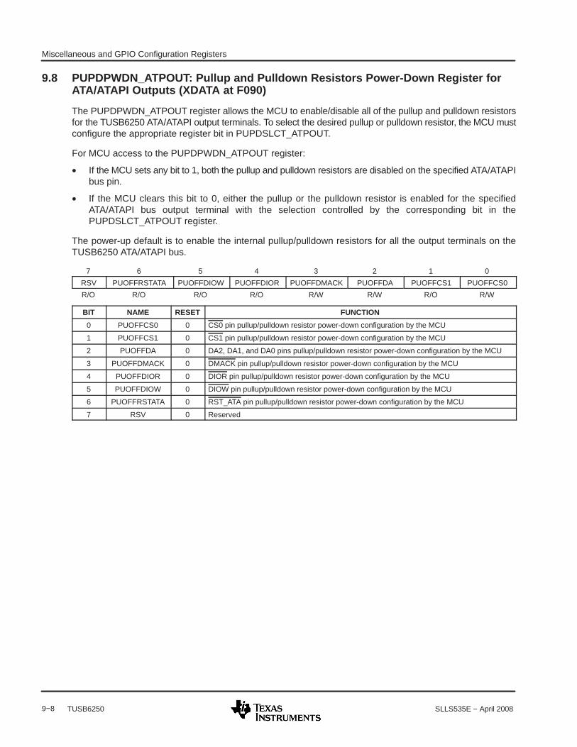
Miscellaneous and GPIO Configuration Registers
9−8 SLLS535E − April 2008TUSB6250
9.8 PUPDPWDN_ATPOUT: Pullup and Pulldown Resistors Power-Down Register forATA/ATAPI Outputs (XDATA at F090)
The PUPDPWDN_ATPOUT register allows the MCU to enable/disable all of the pullup and pulldown resistorsfor the TUSB6250 ATA/ATAPI output terminals. To select the desired pullup or pulldown resistor, the MCU mustconfigure the appropriate register bit in PUPDSLCT_ATPOUT.
For MCU access to the PUPDPWDN_ATPOUT register:
• If the MCU sets any bit to 1, both the pullup and pulldown resistors are disabled on the specified ATA/ATAPIbus pin.
• If the MCU clears this bit to 0, either the pullup or the pulldown resistor is enabled for the specifiedATA/ATAPI bus output terminal with the selection controlled by the corresponding bit in thePUPDSLCT_ATPOUT register.
The power-up default is to enable the internal pullup/pulldown resistors for all the output terminals on theTUSB6250 ATA/ATAPI bus.
7 6 5 4 3 2 1 0
RSV PUOFFRSTATA PUOFFDIOW PUOFFDIOR PUOFFDMACK PUOFFDA PUOFFCS1 PUOFFCS0
R/O R/O R/O R/O R/W R/W R/O R/W
BIT NAME RESET FUNCTION
0 PUOFFCS0 0 CS0 pin pullup/pulldown resistor power-down configuration by the MCU
1 PUOFFCS1 0 CS1 pin pullup/pulldown resistor power-down configuration by the MCU
2 PUOFFDA 0 DA2, DA1, and DA0 pins pullup/pulldown resistor power-down configuration by the MCU
3 PUOFFDMACK 0 DMACK pin pullup/pulldown resistor power-down configuration by the MCU
4 PUOFFDIOR 0 DIOR pin pullup/pulldown resistor power-down configuration by the MCU
5 PUOFFDIOW 0 DIOW pin pullup/pulldown resistor power-down configuration by the MCU
6 PUOFFRSTATA 0 RST_ATA pin pullup/pulldown resistor power-down configuration by the MCU
7 RSV 0 Reserved

I2C Interface Controller
10−1SLLS535E − April 2008 TUSB6250
10 I2C Interface ControllerThe master-only I2C interface controller in the TUSB6250 provides a simple two-wire serial interface for theMCU to communicate with the external EEPROM. It supports single-byte or multiple-byte read and writeoperations. The I2C interface controller can be programmed to operate at either 100 Kbit/sec or 400 Kbit/sec.In addition, the protocol supports 8-bit or 16-bit addressing for accessing the I2C slave device memorylocations. The embedded I2C interface controller however, does not support a multimaster bus environment(no bus arbitration).
The main function of the I2C interface controller is to provide the data path for the descriptor and applicationfirmware to be downloaded from the external I2C EEPROM to the internal on-chip code RAM. The TUSB6250only supports widely available 3.3-V I2C serial EEPROMs. The two interface signals provided by the I2Cinterface controller are the serial clock signal (SCL) and the serial data signal (SDA). The SCL signal is outputonly open-drain. The SDA signal is a bidirectional signal that uses an open-drain output to allow the TUSB6250to be wire-ORed with other I2C slave devices that use open-drain or open-collector outputs. Internal weak100-µA pullup resistors are built into both the SCL and SDA pins. The pullup resistors are always activatedafter a power-up reset.
All read and write data transfers on the I2C serial bus are initiated by the master device. The master deviceis also responsible for generating the clock signal used for all data transfers. The data is transferred on thebus serially, one bit at a time. However, the protocol requires that the address and data be transferred in byte(8 bit) format with the most-significant bit (MSB) transferred first. In addition, each byte transferred on the busis acknowledged by the receiving device with an acknowledge bit.
Each transfer operation begins with the master device driving a start condition on the bus and ends with themaster device driving a stop condition on the bus. During I2C serial data transmission, the SDA line must bestable while the SCL signal is high, which also means that the SDA signal can only change state while the SCLsignal is low.
• The start condition of the I2C serial transmission is defined as a high-to-low transition of the SDA signalwhile the SCL signal is high.
• The stop condition is defined as a low-to-high transition of the SDA signal, while the SCL signal is high.
• The acknowledge is defined as a stable low of the SDA line driven by the receiver after each byte has beenreceived, except when the receiver is unable to receive or transmit or after the master-receiver receivesthe last byte. The transmitter must release the SDA line during the acknowledge clock phase.
For the detailed behavior and protocol of the I2C data transmission, see the industry standard I2C busspecification.
Based on the I2C convention, there are normally two types of I2C devices:
• Category II device: For those I2C EEPROMs with a size less than 4K bytes (up to 11 EEPROM addressbits could be used).
• Category III device: For those I2C EEPROMs with a size equal to or larger than 4K bytes (up to 16EEPROM address bits could be used).
For application firmware with sizes equal to or larger than 4K bytes, the TUSB6250 boot code requires thatthe application firmware be stored in an external I2C EEPROM, with its device address A0 pin (the leastsignificant device address input pin or chip select-0 as referred to in some I2C EEPROM’s data manual) tiedto 1. This indicates to the boot code that the I2C EEPROM connected to the I2C interface of the TUSB6250is a category III I2C EEPROM.
Developers should not confuse the I2C device address with the I2C EEPROM address. The I2C device addressis the address for a particular I2C EEPROM device, which should be set up in the I2CADR register and sentto the I2C EEPROM. The I2C EEPROM address is the I2C internal EEPROM memory cell address, whichshould be set up in the I2CDOUT register and sent to the I2C EEPROM during data phase communication.
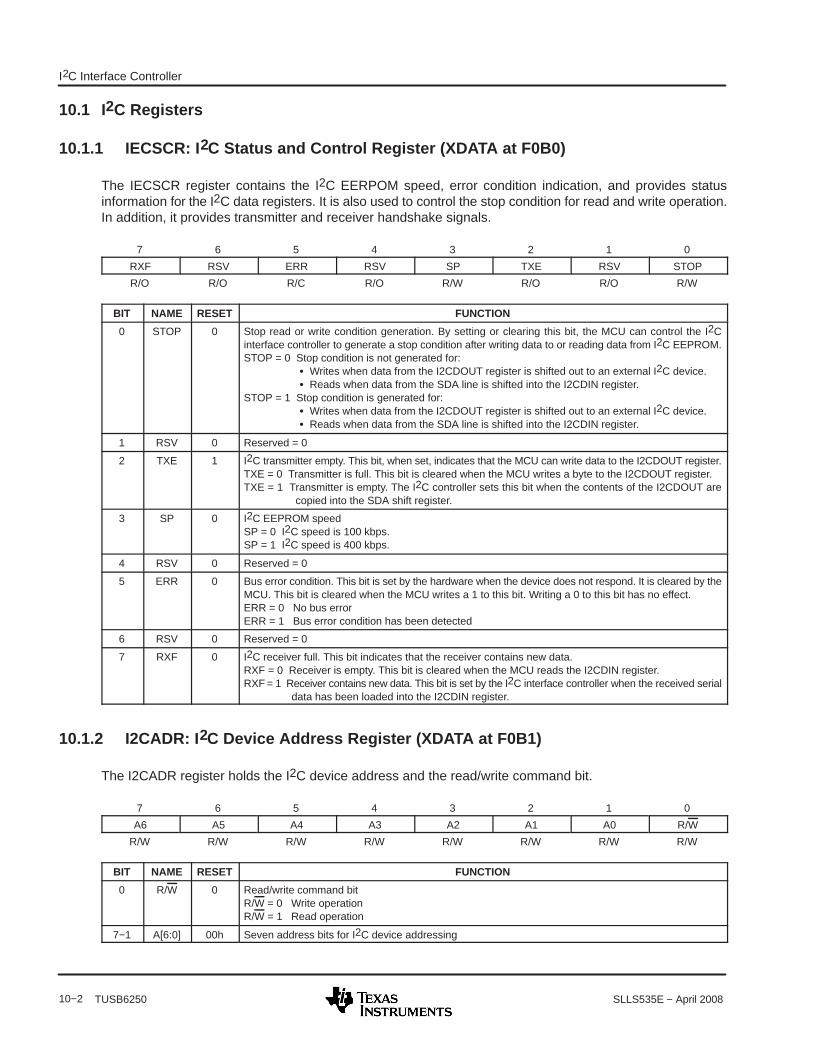
I2C Interface Controller
10−2 SLLS535E − April 2008TUSB6250
10.1 I2C Registers
10.1.1 IECSCR: I2C Status and Control Register (XDATA at F0B0)
The IECSCR register contains the I2C EERPOM speed, error condition indication, and provides statusinformation for the I2C data registers. It is also used to control the stop condition for read and write operation.In addition, it provides transmitter and receiver handshake signals.
7 6 5 4 3 2 1 0
RXF RSV ERR RSV SP TXE RSV STOP
R/O R/O R/C R/O R/W R/O R/O R/W
BIT NAME RESET FUNCTION
0 STOP 0 Stop read or write condition generation. By setting or clearing this bit, the MCU can control the I2Cinterface controller to generate a stop condition after writing data to or reading data from I2C EEPROM.STOP = 0 Stop condition is not generated for:
Writes when data from the I2CDOUT register is shifted out to an external I2C device. Reads when data from the SDA line is shifted into the I2CDIN register.
STOP = 1 Stop condition is generated for: Writes when data from the I2CDOUT register is shifted out to an external I2C device. Reads when data from the SDA line is shifted into the I2CDIN register.
1 RSV 0 Reserved = 0
2 TXE 1 I2C transmitter empty. This bit, when set, indicates that the MCU can write data to the I2CDOUT register.TXE = 0 Transmitter is full. This bit is cleared when the MCU writes a byte to the I2CDOUT register.TXE = 1 Transmitter is empty. The I2C controller sets this bit when the contents of the I2CDOUT are
copied into the SDA shift register.
3 SP 0 I2C EEPROM speedSP = 0 I2C speed is 100 kbps.SP = 1 I2C speed is 400 kbps.
4 RSV 0 Reserved = 0
5 ERR 0 Bus error condition. This bit is set by the hardware when the device does not respond. It is cleared by theMCU. This bit is cleared when the MCU writes a 1 to this bit. Writing a 0 to this bit has no effect.ERR = 0 No bus errorERR = 1 Bus error condition has been detected
6 RSV 0 Reserved = 0
7 RXF 0 I2C receiver full. This bit indicates that the receiver contains new data.RXF = 0 Receiver is empty. This bit is cleared when the MCU reads the I2CDIN register.RXF = 1 Receiver contains new data. This bit is set by the I2C interface controller when the received serial
data has been loaded into the I2CDIN register.
10.1.2 I2CADR: I2C Device Address Register (XDATA at F0B1)
The I2CADR register holds the I2C device address and the read/write command bit.
7 6 5 4 3 2 1 0
A6 A5 A4 A3 A2 A1 A0 R/W
R/W R/W R/W R/W R/W R/W R/W R/W
BIT NAME RESET FUNCTION
0 R/W 0 Read/write command bitR/W = 0 Write operationR/W = 1 Read operation
7−1 A[6:0] 00h Seven address bits for I2C device addressing

I2C Interface Controller
10−3SLLS535E − April 2008 TUSB6250
10.1.3 I2CDIN: I2C Data_In Register (XDATA at F0B2)
The I2CDIN register holds the received data returned by read operation to the external I2C EEPROM.
7 6 5 4 3 2 1 0
D7 D6 D5 D4 D3 D2 D1 D0
R/O R/O R/O R/O R/O R/O R/O R/O
BIT NAME RESET FUNCTION
7−0 D[7:0] 00h Read data returned from I2C EEPROM
10.1.4 I2CDOUT: I2C Data_Out Register (XDATA at F0B3)
The I2CDOUT register holds the data to be transmitted to the external I2C EEPROM for write operation.Writing to the I2CDOUT register starts the transfer on the SDA line.
7 6 5 4 3 2 1 0
D7 D6 D5 D4 D3 D2 D1 D0
W/O W/O W/O W/O W/O W/O W/O W/O
BIT NAME RESET FUNCTION
7−0 D[7:0] 00h Write data to be transmitted to the I2C EEPROM

I2C Interface Controller
10−4 SLLS535E − April 2008TUSB6250
10.2 Random-Read Operation
A random read requires a dummy byte-write sequence to load in the data word address. Once thedevice-address word and the data-word address are clocked out and acknowledged by the device, the MCUstarts a current-address sequence. The following describes the sequence of events to accomplish thistransaction.
Device Address + EEPROM [High Byte]
• The TUSB6250 hardware detects 3-ms bus idle.
• The MCU sets I2CSCR [STOP] = 0. This forces the I2C interface controller not to generate a stopcondition after either the contents of the I2CDIN register are received or contents of the I2CDOUTregister are transmitted.
• The MCU writes the device address (R/W bit = 0) to the I2CADR register (write operation).
• The MCU writes the high byte of the I2C EEPROM address into the I2CDOUT register (this starts thetransfer on the SDA line).
• The TXE bit in the I2CSCR register is cleared (indicates busy).
• The contents of the I2CADR register are transmitted to the I2C EEPROM (preceded by a startcondition on SDA).
• The contents of the I2CDOUT register are transmitted to the I2C EEPROM (EEPROM address).
• The TXE bit in the I2CSCR register is set and interrupts the MCU, indicating that the I2CDOUT registerhas been transmitted.
• Stop condition is not generated.
EEPROM [Low Byte]
• The MCU writes the low byte of the I2C EEPROM address into the I2CDOUT register.
• The TXE bit in the I2CSCR register is cleared (indicates busy).
• The contents of the I2CDOUT register are transmitted to the I2C EEPROM (EEPROM address).
• The TXE bit in the I2CSCR register is set and interrupts the MCU, indicating that the I2CDOUT registerhas been transmitted.
• This completes the dummy write operation. At this point, the I2C EEPROM address is set and the MCUcan perform either a single- or a sequential-read operation.
10.3 Current-Address Read Operation
Once the I2C EEPROM address is set, the MCU can read a single byte by executing the following steps:
1. The MCU sets I2CSCR [STOP] = 1. This forces the I2C controller to generate a stop condition afterthe I2CDIN register contents are received.
2. The MCU writes the device address (R/W bit = 1) to the I2CADR register (read operation).
3. The MCU writes a dummy byte to the I2CDOUT register (this starts the transfer on SDA line).
4. The RXF bit in the I2CSTA register is cleared.
5. Contents of the I2CADR register are transmitted to the device (preceded by a start condition on SDA).
6. Data from the I2C EEPROM are latched into the I2CDIN register (a stop condition is transmitted).
7. The RXF bit in the I2CSCR register is set and interrupts the MCU, indicating that the data is available.
8. The MCU reads the I2CDIN register. This clears the RXF bit (I2CSCR [RXF] = 0).
9. End

I2C Interface Controller
10−5SLLS535E − April 2008 TUSB6250
10.4 Sequential-Read Operation
Once the I2C EEPROM address is set, the MCU can execute a sequential-read operation by executing thefollowing steps (this example illustrates a 32-byte sequential read):
Device Address
• The MCU sets I2CSCR [STOP] = 0. This forces the I2C controller to not generate a stop condition afterthe I2CDIN register contents are received.
• The MCU writes the device address (R/W bit = 1) to the I2CADR register (read operation).
• The MCU writes a dummy byte to the I2CDOUT register (this starts the transfer on the SDA line).
• The RXF bit in the I2CSCR register is cleared.
• The contents of the I2CADR register are transmitted to the device (preceded by a start condition onSDA).
N-Byte Read (31 Bytes)
• Data from the device is latched into the I2CDIN register (stop condition is not transmitted).
• The RXF bit in the I2CSCR register is set and interrupts the MCU, indicating that data is available.
• The MCU reads the I2CDIN register. This clears the RXF bit (I2CSCR [RXF] = 0).
• This operation repeats 31 times.
Last-Byte Read (Byte 32)
• The MCU sets I2CSCR [STOP] = 1. This forces the I2C controller to generate a stop condition afterthe I2CDAI register contents are received.
• Data from the device is latched into the I2CDIN register (a stop condition is transmitted).
• The RXF bit in the I2CSCR register is set and interrupts the MCU, indicating that data is available.
• The MCU reads the I2CDIN register. This clears the RXF bit (I2CSCR [RXF] = 0).
• End

I2C Interface Controller
10−6 SLLS535E − April 2008TUSB6250
10.5 Byte-Write Operation
The byte-write operation involves three phases: device address + EEPROM [high byte] phase, EEPROM [lowbyte] phase, and EEPROM [DATA] phase. The following describes the sequence of events to accomplish thebyte-write transaction.
Device Address + EEPROM [High Byte]
• The MCU sets I2CSCR [STOP] = 0. This forces the I2C interface controller not to generate a stopcondition after the contents of the I2CDOUT register are transmitted.
• The MCU writes the device address (R/W bit = 0) to the I2CADR register (write operation).
• The MCU writes the high byte of the I2C EEPROM address into the I2CDOUT register (this starts thetransfer on the SDA line).
• The TXE bit in the I2CSCR register is cleared (indicates busy).
• The contents of the I2CADR register are transmitted to the I2C EEPROM (preceded by a startcondition on SDA).
• The contents of the I2CDOUT register are transmitted to the I2C EEPROM (EEPROM high address).
• The TXE bit in the I2CSCR register is set and interrupts the MCU, indicating that the I2CDOUT registercontents have been transmitted.
EEPROM [Low Byte]
• The MCU writes the low byte of the I2C EEPROM address into the I2CDOUT register.
• The TXE bit in the I2CSCR register is cleared (indicating busy).
• The contents of the I2CDOUT register are transmitted to the I2C EEPROM (EEPROM low address).
• The TXE bit in the I2CSCR register is set and interrupts the MCU, indicating that the I2CDOUT registercontents have been transmitted.
EEPROM [DATA]
• The MCU sets I2CSCR [STOP] = 1. This forces the I2C interface controller to generate a stop conditionafter the contents of I2CDOUT register are transmitted.
• The data to be written to I2C EEPROM is written by the MCU into the I2CDOUT register.
• The TXE bit in the I2CSCR register is cleared (indicates busy).
• The contents of the I2CDOUT register are transmitted to the I2C EEPROM (EEPROM data).
• The TXE bit in the I2CSCR register is set and interrupts the MCU, indicating that the I2CDOUT registercontents have been transmitted.
• The I2C interface controller generates a stop condition after the contents of the I2CDOUT register aretransmitted.
• End

I2C Interface Controller
10−7SLLS535E − April 2008 TUSB6250
10.6 Page-Write Operation
The page-write operation is initiated in the same way as the byte-write operation, with the exception that a stopcondition is not generated after the first I2C EEPROM [DATA] is transmitted. The following describes thesequence of writing 32 bytes in page mode.
Device Address + EEPROM [High Byte]
• The MCU sets I2CSCR [STOP] = 0. This forces the I2C interface controller not to generate a stopcondition after the contents of the I2CDOUT register are transmitted.
• The MCU writes the device address (R/W bit = 0) to the I2CADR register (write operation).
• The MCU writes the high byte of the I2C EEPROM address into the I2CDOUT register.
• The TXE bit in the I2CSCR register is cleared (indicating busy).
• The contents of the I2CADR register are transmitted to the I2C EEPROM (preceded by a startcondition on SDA).
• The contents of the I2CDOUT register are transmitted to the I2C EEPROM (EEPROM address).
• The TXE bit in the I2CSCR register is set and interrupts the MCU, indicating that the I2CDOUT registercontents have been transmitted.
EEPROM [Low Byte]
• The MCU writes the low byte of the I2C EEPROM address into the I2CDOUT register.
• The TXE bit in the I2CSCR register is cleared (indicates busy).
• The contents of the I2CDOUT register are transmitted to the I2C EEPROM (EEPROM address).
• The TXE bit in the I2CSCR register is set and interrupts the MCU, indicating that the I2CDOUT registercontents have been transmitted.
EEPROM [DATA] − 31 Bytes
• The data to be written to the I2C EEPROM is written by the MCU into the I2CDOUT register.
• The TXE bit in the I2CSCR register is cleared (indicates busy).
• The contents of the I2CDOUT register are transmitted to the I2C EEPROM (EEPROM data).
• The TXE bit in the I2CSCR register is set and interrupts the MCU, indicating that the I2CDOUT registercontents have been transmitted.
• This operation repeats 31 times.
EEPROM [DATA] − Last Byte
• The MCU sets I2CSCR [STOP] = 1. This forces the I2C interface controller to generate a stop conditionafter the contents of the I2CDOUT register are transmitted.
• The MCU writes the last date byte to be written to the I2C EEPROM into the I2CDOUT register.
• The TXE bit in the I2CSCR register is cleared (indicates busy).
• The contents of the I2CDOUT register are transmitted to I2C EEPROM (EEPROM data)
• The TXE bit in the I2CSCR register is set and interrupts the MCU, indicating that the I2CDOUT registercontents have been transmitted.
• The I2C interface controller generates a stop condition after the contents of I2CDOUT register aretransmitted.
• End of 32-byte page-write operation

I2C Interface Controller
10−8 SLLS535E − April 2008TUSB6250
10.7 I2C EEPROM Head Block
To fully use the maximum speed of the variety of I2C EEPROMs on the market, the I2C interface controllerin the TUSB6250, along with boot code and firmware, features a special mechanism to detect the speedsupported by the I2C EEPROM connected to its I2C port. In order that the auto-detect mechanism workscorrectly, it is required that any I2C EEPROM connected to the I2C port with valid data stored, must have afixed 2-byte signature at address 0 of the I2C EEPROM.
Table 10−1. I2C EEPROM Signature in Descriptor BlockI2C EEPROM ADDRESS REQUIRED SIGNATURE IN I2C EEPROM
Byte 0 (hex) 0x50
Byte 1 (hex) 0x62
Byte 2 (hex) Starting I2C EEPROM header/descriptor block
… …NOTE: For detailed information regarding the I2C EEPROM header/descriptor block, see
the TUSB6250 Boot Code application note (SLLA126).
During the power-up boot-up sequence, the boot code uses the following sequences to determine whetherthe I2C EEPROM connected has any valid data.
1. Reads byte 0 and byte 1 in the I2C EEPROM with 100 Kbits/sec speed (based on the default reset valueof SP bit in the I2CSCR register) to see whether the connected I2C EEPROM returns a valid signature0x6250.
a. If a valid signature is returned, the boot code concludes that the I2C EEPROM contains valid data.
b. The boot code then operates according to the boot sequence defined in the TUSB6250 boot codedocument.
2. If the foregoing read does not return the valid signature, the boot code considers that either the I2CEEPROM is blank or there is no I2C EEPROM connected at the TUSB6250 I2C port.

ATA/ATAPI Interface Port
11−1SLLS535E − March 2008 TUSB6250
11 ATA/ATAPI Interface Port
The ATA/ATAPI controller embedded in the TUSB6250 acts as a bridge between the device USB interface andATA/ATAPI interface. A high-performance DMA engine is implemented in the ATA/ATAPI controller to movedata automatically between the TUSB6250 sector FIFO and the ATA/ATAPI interface port where the externalATA/ATAPI mass storage device is connected.
Unlike other state-machine-based USB 2.0 ATA/ATAPI mass storage bridge controllers on the market, theTUSB6250 offers both the performance achieved by using a DMA state machine, and the flexibility providedthrough the MCU and firmware control.
Figure 11−1 illustrates the data flow between the TUSB6250 USB interface and a mass storage device (forexample, a hard disk drive) connected to the controller ATA/ATAPI port. Figure 11−2 illustrates all major blocksin the ATA/ATAPI controller. The TUSB6250 supports the USB mass storage class bulk-only transportprotocol, which consists of three stages for each data transfer: command, data, and status.
• In the command stage, the host commands to the drive are processed by the MCU. The commands issuedby the USB host are transferred through the USB bulk pipe to the addressed USB bulk endpoint. The MCUdispatches the commands to the proper ATA/ATAPI registers.
• In the data stage, the TUSB6250 allows data to be transferred:
− Manually by firmware. As such, the data movement between the upstream USB interface and the 4Kbyte EDB is processed by the UBM. However, the data between the 4K-byte EDB and the ATA/ATAPIinterface is processed by the MCU.
− Automatically by the DMA engine in the ATA/ATAPI controller. As such, the UBM moves the databetween the upstream USB interface and the sector FIFO. Then, the data is automatically movedbetween the sector FIFO and the ATA/ATAPI interface by the DMA engine without MCU intervention.
• In the status stage, when a command is terminated, the ATA/ATAPI controller interrupts the MCU withcommand completion or error information. The MCU then performs reads from the ATA/ATAPI drive statusregisters and reports back to the USB host via the addressed USB bulk-in endpoint.
Note that the sector data transfer is a half-duplex operation. The dotted line between the MCU and the sectorFIFO in the diagram indicates that the MCU can only access the sector FIFO indirectly by using the MCUaccess address and data registers defined in the ATA/ATAPI group-2 register section.
USB8K/24K/32K-ByteSize-ConfigurableSector FIFO RAM
UBM
ATA/ATAPIController
State Machineand DMA Engine
IDE
MCU
4K-ByteEDB
Figure 11−1. ATA/ATAPI-Port Data Flow Diagram

ATA/ATAPI Interface Port
11−2 SLLS535E − March 2008TUSB6250
11.1 TUSB6250 ATA Controller Architecture Overview
The TUSB6250 ATA/ATAPI controller contains three state machines, the ATA/ATAPI CSR registers, and thesector FIFO controller, as illustrated in Figure 11−2. The sector FIFO controller is the high-performance DMAengine discussed in the previous section.
Ultra DMAState Machine
PIO-DMAState Machine
TransactionState Machine
Sector FIFORAM
TUSB6250 ATA/ATAPI Controller
Sector FIFOController
ATA/ATAPICSR Registers
ATA/ATAPIPort
MCU
Figure 11−2. TUSB6250 ATA/ATAPI Controller Block Diagram
11.1.1 ATA/ATAPI Controller State Machine
The following state machines are responsible for command and data transfer between the ATA/ATAPIinterface port and the TUSB6250 internal logic.
• Transaction state machine— The transaction state machine handles command level transactions. Italso controls the PIO-DMA state machine and the ultra DMA state machine to perform actual data transferbetween the TUSB6250 internal logic and the ATA/ATAPI interface port.
• PIO-DMA state machine— The PIO-DMA state machine handles PIO transfers and multiword DMAtransfers.
• Ultra DMA state machine— The ultra DMA state machine handles ultra DMA transfers.
11.1.2 Sector FIFO Controller
As described in Section 6.1, MCU Memory Map, the sector FIFO RAM is used as the data buffer for the databeing transferred between the TUSB6250 ATA/ATAPI interface and the USB interface in the automaticdata-transfer mode. The name sector FIFO implies it is derived from the data buffer for the sector data of anATA hard-disk drive, although the sector FIFO of the TUSB6250 can actually be used for either ATA or ATAPIdata buffering in the automatic data transfer mode. The TUSB6250 features a unique size-configurable sectorFIFO to allow efficient code and data space usage. The sector FIFO size can be partitioned as 8K bytes,24K bytes, or 32K bytes.
ATA/ATAPI Interface Port
11−3SLLS535E − March 2008 TUSB6250
The sector FIFO can be accessed by the UBM, ATA/ATAPI controller, and the MCU, where the MCU can onlybe indirectly accessed by going through the ATA/ATAPI CSR and the sector FIFO controller. The UBM accesshas the highest priority, the ATA/ATAPI controller has the middle level access priority, and the MCU accesshas the lowest priority.
11.1.3 ATA/ATAPI CSR Registers
The ATA/ATAPI CSR register block contains all the ATA/ATAPI control and status registers, which arecategorized into three register groups based on their function.
• ATA/ATAPI group 0 registers— This group consists of 16 Task_File registers, which are normally usedto pass commands along with the related parameters to the ATA/ATAPI drives in auto-command modesthat are described in Section 11.3, TUSB6250 ATA/ATAPI Controller Transfer Modes.
• ATA/ATAPI group 1 registers —The 16 registers of this group normally are used to configure theATA/ATAPI interface (for example, transfer mode, speed and timing, etc.) and set up the parametersneeded for the data transfer to be performed (for example, transfer byte-count, command length, blocksector count, etc.).
• ATA/ATAPI group 2 registers— The 26 registers of this group normally are used to check the status ofthe drive and data transfer through the ATA/ATAPI interrupt registers. The group also includes theregisters to enable the MCU access to the sector FIFO. There are some registers that allow the firmwareto handle all 13 cases of the bulk-only transfer protocol specification when there is any error condition onthe ATA/ATAPI drive side.
As described previously, the MCU can access the sector FIFO only indirectly by using its address and dataregisters in the ATA/ATAPI group 2 registers (MCU data byte_n registers and the MCU access addresslow-/high-byte registers).

ATA/ATAPI Interface Port
11−4 SLLS535E − March 2008TUSB6250
11.2 ATA/ATAPI Port Power-On Sequencing and 3-State Control
As described in Section 5.3.1, Unique Power-On Sequencing to the Storage Device, the TUSB6250 offersunique power-on sequencing features, which provides design flexibility to the drive developers, especially ifmultiple devices share the ATA/ATAPI bus. Unlike other USB-to-ATA/ATAPI bridge controllers, the TUSB6250powers up with its ATA/ATAPI interface totally disabled and with its output buffers in the high-impedance state.The internal pulldown resistors are also enabled by default after the power-up reset. Once the firmware isloaded into the code RAM, it then has the control to enable the ATA/ATAPI bus and reconfigure all the GPIOsalong with the pullup and pulldown resistors at any time required by the application.
Another key feature of the TUSB6250 is that it allows the firmware to disable the entire ATA/ATAPI bus andput it into the high-impedance state during normal operation, simply by setting the ATP_DIS bit in theCMNDLNGTH (command length) register. To reenable the interface, the firmware must clear the ATP_DISbit. The TUSB6250 also provides pullup and/or pulldown resistors on most of its ATA/ATAPI interface pins,which sets it apart from other mass-storage controller chips.
The advantages of the above features are as follows:
• The ATA/ATAPI interface powering up in the high-impedance state enables the end-product applicationto meet the critical 100-mA bus-power current consumption limit required by the USB 2.0 specification.Otherwise, if a hard-disk drive is powered up and performs a start-up disk spin-up at the same time, whilethe TUSB6250 is powering up, the surge current is likely to exceed 100 mA.
• This also protects the mass-storage device connected to the TUSB6250 ATA/ATAPI interface fromdamage, if the mass-storage device is not equipped with fail-safe I/O buffers.
• The firmware controllable 3-state feature allows the TUSB6250 to share the ATA/ATAPI bus with anotherTI DSP or microcontroller implemented on the same end-product PCB.
The ATA/ATAPI bus 3-state control feature can also be implemented based on an external event. For example,if an onboard DSP shares the same ATA/ATAPI bus with the TUSB6250 in a portable digital audio playerapplication, the end product could use the remote-wakeup-capable P3.5 pin as an ATA/ATAPI bus-requestsignal to alert the TUSB6250 when the DSP needs the ATA/ATAPI bus. The TUSB6250, under flexiblefirmware control, finishes the current data-transferring task it is performing and then grants the ATA/ATAPI busto the DSP. Vise versa, the TUSB6250 can also use another GPIO as the bus-request signal to alert the DSPwhen it needs the ATA/ATAPI bus. With the many GPIOs the TUSB6250 offers, flexible handshake functionsbetween the two on-board controllers are easily accomplished.
Figure 11−3 illustrates the power up and reset sequences for the TUSB6250 ATA/ATAPI interface.

ATA/ATAPI Interface Port
11−5SLLS535E − March 2008 TUSB6250
PWR100
Pulled High byExternal Pullup
Resistor
PWR500
Signal-Connectto the USB Host
TUSB6250 Configuredby the USB Host
RST_ATA
t0
Pulled Low byInternal Pulldown
Resistor
Driven Low byTUSB6250 UnderFirmware Control
Figure 11−3. ATA/ATAPI Bus Power-Up and Reset Sequence
Note that the PWR500 function showed in the Figure 11−3 is not implemented in the TUSB6250 hardware.The option of whether to implement this functionality in the firmware as described is up to the end-productdeveloper. The detailed ATA/ATAPI bus behavior is described as follows for reference. Figure 11−3 assumesthe power-up reset to the TUSB6250 is finished and the controller is in the boot sequence under the controlof boot code at the beginning, which is marked as the time t0 as shown:
• After power-up reset, the whole ATA/ATAPI interface of the TUSB6250 is disabled with all output buffersturned off. Internal 200-µA pulldown resistors are enabled on all signals of the ATA/ATAPI bus to avoidbus floating. As shown in Figure 11−3, the output buffer on the RST_ATA signal is also turned off with theinternal pulldown resistor enabled.
• Both the PWR100 and PWR500 pins are open-drain outputs without internal pullup or pulldown resistors.Their open-drain buffers are turned off during power-up reset. It is the developer’s responsibility to haveexternal pullup resistors to pull these two signals up during power up.
• Whenever VBUS is detected from the upstream USB bus, the boot code drives PWR100 low to indicatethat the controller is in the enumeration stage and allowed to consume 100 mA from the VBUS. This canalso serve as an alert signal to let the ATA/ATAPI device connected to the TUSB6250 ATA/ATAPI interfaceprepare for the upcoming ATA/ATAPI power-up reset sequencing.
• When the TUSB6250 is fully configured by the upstream USB host, the end-product-specific applicationfirmware could choose to drive the PWR500 signal to low, which could be used to indicate that thecomplete end product is allowed to draw 500 mA for a bus-powered application. This signal, ifimplemented in firmware, can also act as a power-control signal to turn on the ATA/ATAPI drive.
• Once the TUSB6250 is fully configured and the application firmware is fully loaded, the boot code handsover the control to the application firmware, which reconfigures all GPIOs and pullup and pulldownresistors to meet the application requirement. When the firmware is ready, it drives the RST_ATA pin lowby setting the HARD_RST bit in the ATPIFCNFG1 register. The firmware then enables the ATA/ATAPI busby clearing the ATP_DIS bit in the CMNDLNGTH register to start the ATA/ATAPI power-up resetsequencing. The firmware then clears the HARD_RST bit tode-assert RST_ATA when the ATA/ATAPIreset duration time is met.
• In case the boot code fails to detect the VBUS during boot time, it leaves the PWR100 alone (withoutdriving it). The firmware, once it has taken over, must perform the power sequencing to the ATAPI driveby asserting these two power-control signals. This applies to both the bus-powered application and theself-powered application.

ATA/ATAPI Interface Port
11−6 SLLS535E − March 2008TUSB6250
11.3 TUSB6250 ATA/ATAPI Controller Transfer Modes
The supported Universal Serial Bus Mass Storage Class Bulk-Only Transport protocol uses only the bulkendpoint for the transport of command, data, and status. The transport command set used in the bulk-onlyprotocol is actually based on the SCSI transparent command set, which is wrapped with some informationrelated to the bulk-only protocol, to form the command block wrapper (CBW) for a specific transport.
At the command stage, the mass storage application at the host side sends a CBW to a USB mass storagedevice. The TUSB6250, as a USB mass-storage bridge controller, performs analysis of the CBWCB receivedfrom the host and translates the CBWCB into a sequence of command block register writes to the ATA/ATAPIstorage device connected to the TUSB6250 ATA/ATAPI interface. The storage device interprets the commandblock register contents as a set of commands and prepares the following data transfer from the host, if thereis any.
A CBW consists of the following major elements:
• dCBWSignature—This is used to help identify the data packet received from the host as a valid CBW.
• dCBWTag—This is a tag associating a specific CBW and command status wrapper (CSW).
• dCBWDataTransferLength—This specifies the number of bytes the host expects to transfer on the bulk-inor bulk-out endpoint.
• bmCBWFlags—This field contains the data transfer direction for the current CBW, which can be eitherfrom the host to the mass storage device or vice versa.
• bCBWLUN—This field specifies the logic unit number to which the command block is being sent.
• bCBWCBLength—This field specifies the valid length of the CBWCB in bytes, which is the valid lengthof the command block. The only legal values are 1 through 16.
• CBWCB—This is the command block to be executed by the device. The device interprets the firstbCBWCBLength bytes in this field as a command block, as defined by the command set identified bybInterfaceSubClass, which is the SCSI transparent command set.
At the status stage, a CSW is sent back to the host with the drive-status-related information. A valid CSWconsists of a valid dCSWSignature, dCSWTag, which is the same as the dCBWTag for a given CBW,dCSWDataResidue, which is the difference of data amount between what the host expects and what the massstorage device actually processed, and the bCSWStatus, which indicates the success or failure of the CBW.For more detailed information, see the Universal Serial Bus Mass Storage Class Bulk-Only Transportspecification.
It should be noted that for the TUSB6250 ATA/ATAPI controller, the status stage is always processed by theMCU, which adds valuable flexibility for the firmware when handling any ATA/ATAPI drive-related errorcondition.
Because the TUSB6250 is equipped with an MCU, state machine, and DMA engine, it supports three kindsof data transfer modes or schemes, based on the amount of involvement from the MCU and state machine:fully-manual mode, semiautomatic mode, and fully automatic mode. These modes, different in the amount ofautomation involved during the command stage and data stage, are the schemes used by the TUSB6250 fora given CBW data transfer, which should not be confused with the PIO or UDMA transfer modes defined inthe ATA/ATAPI-5 specification.
• Fully manual mode— In this mode, the MCU is responsible to handle all the data movement between the4K byte EDB and the ATA/ATAPI interface for the command, data, and status stages. The sector FIFOis not used. The firmware must use ATA/ATAPI access registers 0 to 3 (ATPACSREG0–ATPACSREG3)to perform ATA/ATAPI drive register access. The data transfer throughput is low compared to thesemiautomatic and fully-automatic mode. In order to transfer one byte, the firmware must manually writeeach data byte into the ATA/ATAPI access registers.

ATA/ATAPI Interface Port
11−7SLLS535E − March 2008 TUSB6250
• Semiautomatic mode— In this mode, similar to the fully manual mode, the MCU is also responsible forhandling all data movement between the 4K-byte EDB and the ATA/ATAPI interface for the command andstatus stages. However, during the data stage, the sector FIFO and ATA/ATAPI controller along with theDMA engine are used to process the transfer when the firmware sets the MAP_SECF bit in either theIEPCNFG_n or OEPCNFG_n register and sets the START_ATAPI bit in the ATPIFCNFG1 register. Thefirmware is not required to be involved in the lengthy data stage transfer.
• Fully automatic mode— In this mode, the MCU must handle only the status stage and the partialcommand stage. During the command stage, the firmware is not required to send the CBWCB to the drivemanually. Instead, it must only fill up the correct contents required for the current CBW into the Task_Fileregisters of the group 0 registers. Once the firmware finishes this task, the only thing it is required to dois set the AUTO_CMD and START_ATAPI bits in the ATPIFCNFG1 register. The ATA/ATAPI controller ofthe TUSB6250 then performs the command writes to the ATA/ATAPI drive in the sequence required bythe ATA/ATAPI-5 specification, followed by the data transfer, if any. The MAP_SECF bit must be set ineither the IEPCNFG_n or OEPCNFG_n register in order to use the sector FIFO for the automatic datatransfer in the data stage. When the ATA/ATAPI controller finishes the transfer of the data stage, it triggersthe MCU with an ATA/ATAPI interrupt (vector value of 0x48) with the command completion informationprovided in some of the group-2 registers. The hardware also clears the MAP_SECF bit so that thefollowing status stage and command stage of the next CBW can use the 4K-byte EDB. The firmware thenstarts the status stage task to prepare the information required in the CSW to be sent back to the host.This mode has the highest data transfer throughput among all three modes due to the minimum MCUinvolvement.
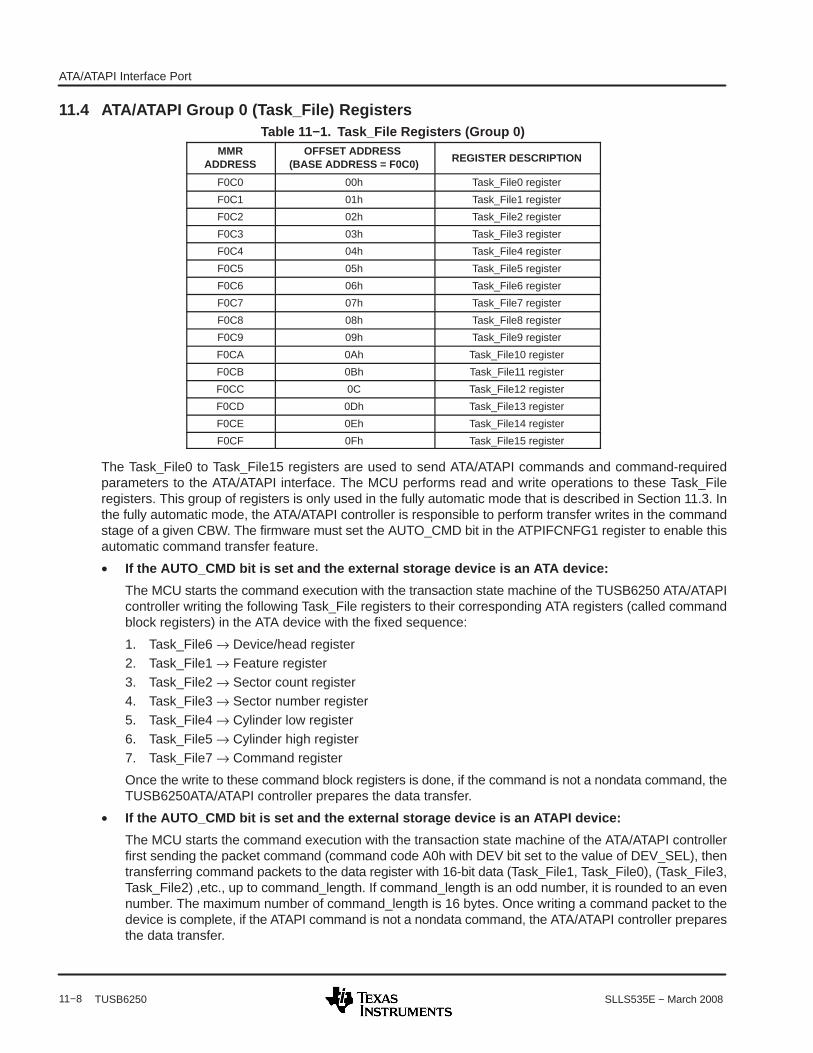
ATA/ATAPI Interface Port
11−8 SLLS535E − March 2008TUSB6250
11.4 ATA/ATAPI Group 0 (Task_File) RegistersTable 11−1. Task_File Registers (Group 0)
MMRADDRESS
OFFSET ADDRESS (BASE ADDRESS = F0C0) REGISTER DESCRIPTION
F0C0 00h Task_File0 register
F0C1 01h Task_File1 register
F0C2 02h Task_File2 register
F0C3 03h Task_File3 register
F0C4 04h Task_File4 register
F0C5 05h Task_File5 register
F0C6 06h Task_File6 register
F0C7 07h Task_File7 register
F0C8 08h Task_File8 register
F0C9 09h Task_File9 register
F0CA 0Ah Task_File10 register
F0CB 0Bh Task_File11 register
F0CC 0C Task_File12 register
F0CD 0Dh Task_File13 register
F0CE 0Eh Task_File14 register
F0CF 0Fh Task_File15 register
The Task_File0 to Task_File15 registers are used to send ATA/ATAPI commands and command-requiredparameters to the ATA/ATAPI interface. The MCU performs read and write operations to these Task_Fileregisters. This group of registers is only used in the fully automatic mode that is described in Section 11.3. Inthe fully automatic mode, the ATA/ATAPI controller is responsible to perform transfer writes in the commandstage of a given CBW. The firmware must set the AUTO_CMD bit in the ATPIFCNFG1 register to enable thisautomatic command transfer feature.
• If the AUTO_CMD bit is set and the external storage device is an ATA device:
The MCU starts the command execution with the transaction state machine of the TUSB6250 ATA/ATAPIcontroller writing the following Task_File registers to their corresponding ATA registers (called commandblock registers) in the ATA device with the fixed sequence:
1. Task_File6 → Device/head register2. Task_File1 → Feature register3. Task_File2 → Sector count register4. Task_File3 → Sector number register5. Task_File4 → Cylinder low register6. Task_File5 → Cylinder high register7. Task_File7 → Command register
Once the write to these command block registers is done, if the command is not a nondata command, theTUSB6250ATA/ATAPI controller prepares the data transfer.
• If the AUTO_CMD bit is set and the external storage device is an ATAPI device:
The MCU starts the command execution with the transaction state machine of the ATA/ATAPI controllerfirst sending the packet command (command code A0h with DEV bit set to the value of DEV_SEL), thentransferring command packets to the data register with 16-bit data (Task_File1, Task_File0), (Task_File3,Task_File2) ,etc., up to command_length. If command_length is an odd number, it is rounded to an evennumber. The maximum number of command_length is 16 bytes. Once writing a command packet to thedevice is complete, if the ATAPI command is not a nondata command, the ATA/ATAPI controller preparesthe data transfer.
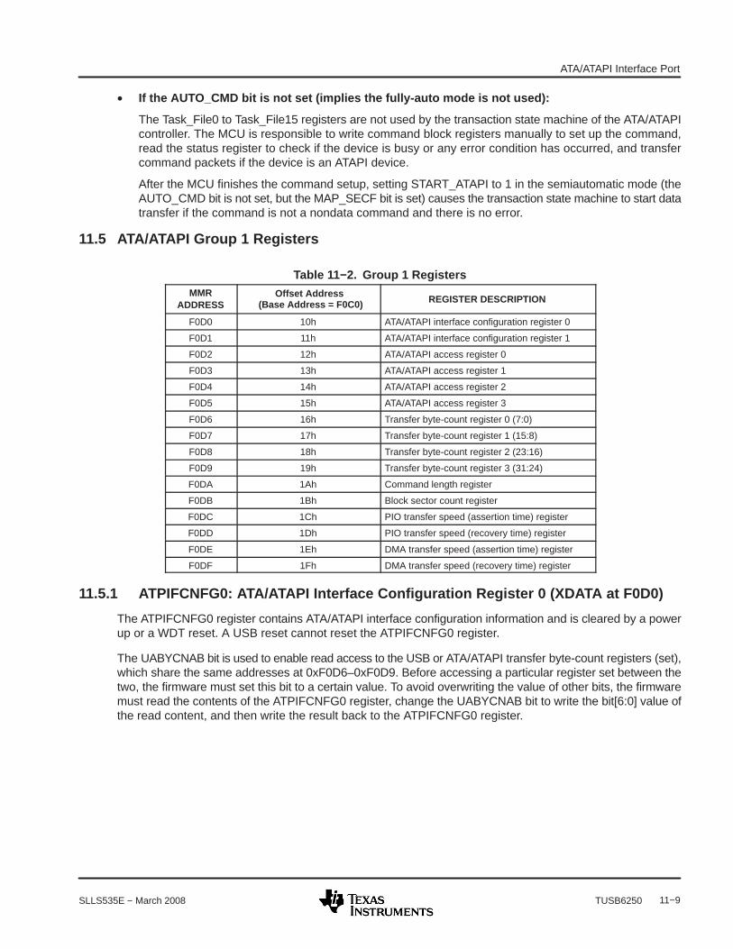
ATA/ATAPI Interface Port
11−9SLLS535E − March 2008 TUSB6250
• If the AUTO_CMD bit is not set (implies the fully-auto mode is not used):
The Task_File0 to Task_File15 registers are not used by the transaction state machine of the ATA/ATAPIcontroller. The MCU is responsible to write command block registers manually to set up the command,read the status register to check if the device is busy or any error condition has occurred, and transfercommand packets if the device is an ATAPI device.
After the MCU finishes the command setup, setting START_ATAPI to 1 in the semiautomatic mode (theAUTO_CMD bit is not set, but the MAP_SECF bit is set) causes the transaction state machine to start datatransfer if the command is not a nondata command and there is no error.
11.5 ATA/ATAPI Group 1 Registers
Table 11−2. Group 1 RegistersMMR
ADDRESSOffset Address
(Base Address = F0C0) REGISTER DESCRIPTION
F0D0 10h ATA/ATAPI interface configuration register 0
F0D1 11h ATA/ATAPI interface configuration register 1
F0D2 12h ATA/ATAPI access register 0
F0D3 13h ATA/ATAPI access register 1
F0D4 14h ATA/ATAPI access register 2
F0D5 15h ATA/ATAPI access register 3
F0D6 16h Transfer byte-count register 0 (7:0)
F0D7 17h Transfer byte-count register 1 (15:8)
F0D8 18h Transfer byte-count register 2 (23:16)
F0D9 19h Transfer byte-count register 3 (31:24)
F0DA 1Ah Command length register
F0DB 1Bh Block sector count register
F0DC 1Ch PIO transfer speed (assertion time) register
F0DD 1Dh PIO transfer speed (recovery time) register
F0DE 1Eh DMA transfer speed (assertion time) register
F0DF 1Fh DMA transfer speed (recovery time) register
11.5.1 ATPIFCNFG0: ATA/ATAPI Interface Configuration Register 0 (XDATA at F0D0)
The ATPIFCNFG0 register contains ATA/ATAPI interface configuration information and is cleared by a powerup or a WDT reset. A USB reset cannot reset the ATPIFCNFG0 register.
The UABYCNAB bit is used to enable read access to the USB or ATA/ATAPI transfer byte-count registers (set),which share the same addresses at 0xF0D6–0xF0D9. Before accessing a particular register set between thetwo, the firmware must set this bit to a certain value. To avoid overwriting the value of other bits, the firmwaremust read the contents of the ATPIFCNFG0 register, change the UABYCNAB bit to write the bit[6:0] value ofthe read content, and then write the result back to the ATPIFCNFG0 register.

ATA/ATAPI Interface Port
11−10 SLLS535E − March 2008TUSB6250
7 6 5 4 3 2 1 0
UABYCNAB RSV RSV RSV USBWPNABRTEN DMADIRCKEN TRANS_MOD1 TRANS_MOD0
R/W R/O R/O R/O R/W R/W R/W R/W
BIT NAME RESET FUNCTION
1−0 TRANS_MOD[1:0] 00 ATA/ATAPI transfer mode.TRANS_MOD = 00 PIO modeTRANS_MOD = 01 Multiword DMA modeTRANS_MOD = 10 ReservedTRANS_MOD = 11 Ultra DMA mode
2 DMADIRCKEN 0 DMA direction check enable.
This bit, when set, enables the TUSB6250 state machine to check the DMA transferdirection matching between the TUSB6250 and the ATAPI device automatically beforeperforming the ATAPI DMA data transfer. If there is a mismatch in DMA data transferdirection, the data transfer is aborted and the ATP_DSEQ_ER in the ATPINTRPT1 registeris set to indicate the error. This bit is not used in ATA data transfer.
3 USBWPNABRTEN 0 USB write pending abort enable.During a write data transfer to an ATA/ATAPI device, if any byte-count mismatch occurs atthe USB interface side of the TUSB6250 the process of moving the last received data packetfrom the sector FIFO to an ATA/ATAPI device is paused to wait for the MCU decision.
This bit, when set, allows the MCU to abort and flush the last received packet into the sectorFIFO.
This bit, when cleared, allows the MCU to move all the data stored in sector FIFO to anATA/ATAPI device up to the dCBWDataTransferLength.
The MCU must ensure it sets this bit properly before clearing the USB_XFR_PND interrupt.
6−4 RSV 000 These three bits must be set to 000 during normal operation.
7 UABYCNAB 0 USB or ATA/ATAPI byte-count register access control bit.UABYCNAB = 0 Enables read access to the USB byte-count register (0xF0D6–0xF0D9).UABYCNAB = 1 Enables read access to the ATAPI byte-count register (0xF0D6–0xF0D9).

ATA/ATAPI Interface Port
11−11SLLS535E − March 2008 TUSB6250
11.5.2 ATPIFCNFG1: ATA/ATAPI Interface Configuration Register 1 (XDATA at F0D1)
7 6 5 4 3 2 1 0
ATP_MOD SOFT_RST HARD_RST XFER_DIR AUTO_CMD START_ATAPI NON_DA_CMD DEV_SEL
R/W W/C R/W R/W R/W W/C R/W R/W
BIT NAME RESET FUNCTION
0 DEV_SEL 0 ATAPI device select.When ATP_MOD = 1 and AUTO_CMD =1 and START_ATAPI =1 and:DEV_SEL = 0 The internal state machine sets the DEV bit of the device/head register to 0 when
it sends the packet command.DEV_SEL = 1 The internal state machine sets the DEV bit of the device/head register to 1 when
it sends the packet command.
1 NON_DA_CMD 0 Non-data command.When START_ATAPI = 1 and:NON_DA_CMD = 0 The internal state machine expects to transfer data between the TUSB6250
and the storage device.NON_DA_CMD = 1 The internal state machine does not transfer data.
2 START_ATAPI 0 Start ATA/ATAPI transfer. Set by the MCU/self-cleared.When this bit is set (START_ATAPI = 1), the internal state machine starts: Sending a command if AUTO_CMD = 1 Transferring data if AUTO_CMD = 0START_ATAPI remains active for one clock cycle. It is cleared thereafter automatically.The data transfer size is determined by the transfer byte count TRNS_BCN[31:0].
3 AUTO_CMD 0 Auto command.When this bit is set (AUTO_CMD = 1), the internal state machine automatically fetches the CBWcommand and command parameters from Task_File0 to Task_File15, which is loaded to thestorage device to start the command execution once the MCU sets START_ATAPI to 1.
4 XFER_DIR 0 ATA/ATAPI data transfer direction.XFER_DIR = 0 Data transfer is from the host (TUSB6250) to the storage device.XFER_DIR = 1 Data transfer is from the storage device to the host (TUSB6250).
5 HARD_RST 0 ATA/ATAPI hardware reset. Set and cleared by the MCU.When this bit is set (HARD_RST = 1), the TUSB6250 drives the RST_ATA pin low, which createsa hard reset to the storage device. To dismiss a hard reset to the storage device, the MCU mustwrite a 0 to the HARD_RST bit.
6 SOFT_RST 0 ATA/ATAPI state machine soft reset. Set by the MCU/self cleared.When this bit is set (SOFT_RST = 1), the internal logic generates a soft reset to: Reset the internal state machines, Reset sector FIFO pointers (to 0), Clear the internal data buffer.The internal soft reset signal lasts one clock cycle. The SOFT_RST bit is automatically clearedto 0 thereafter. The SOFT_RST bit has nothing to do with any reset function to the ATA/ATAPIdevice.
7 ATP_MOD 0 ATAPI mode.ATP_MOD = 0 The storage device uses ATA transfer protocol.ATP_MOD = 1 The storage device uses ATAPI transfer protocol.
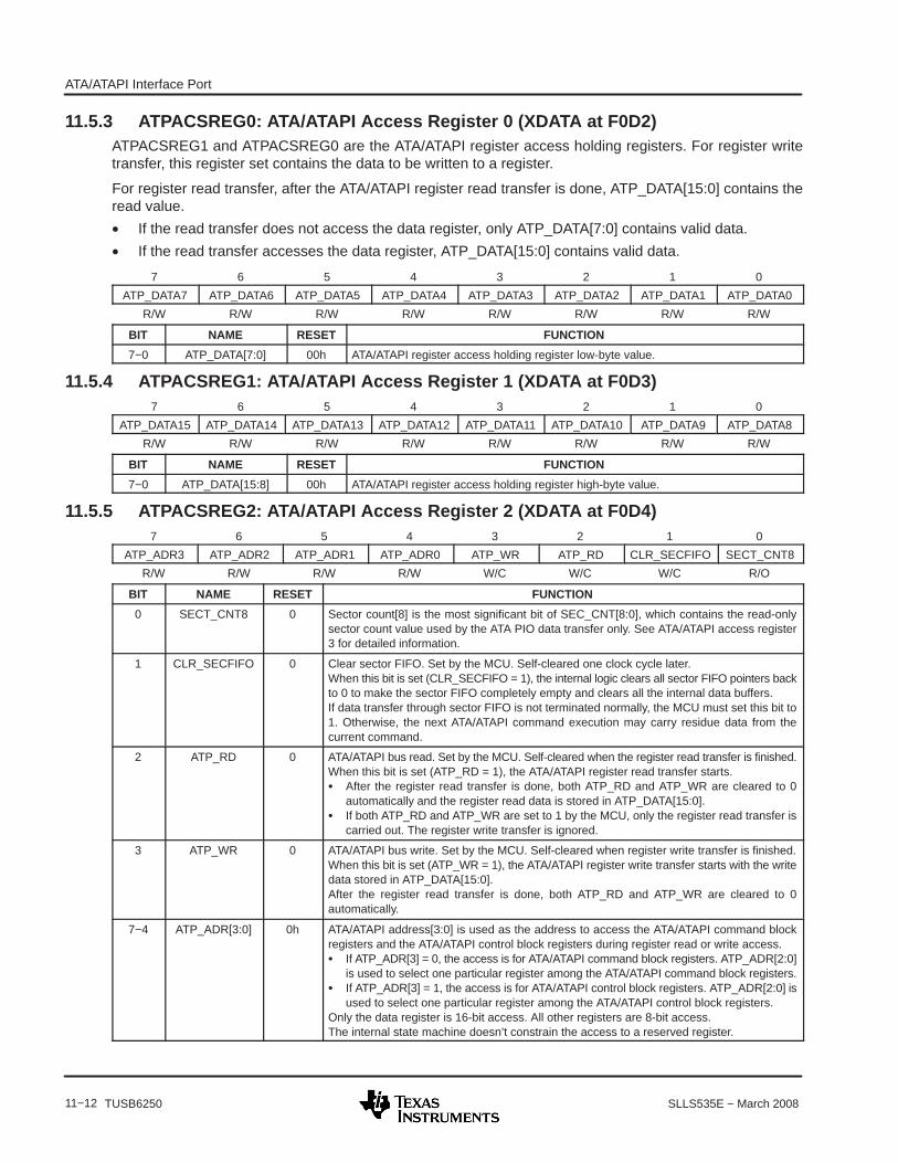
ATA/ATAPI Interface Port
11−12 SLLS535E − March 2008TUSB6250
11.5.3 ATPACSREG0: ATA/ATAPI Access Register 0 (XDATA at F0D2)ATPACSREG1 and ATPACSREG0 are the ATA/ATAPI register access holding registers. For register writetransfer, this register set contains the data to be written to a register.
For register read transfer, after the ATA/ATAPI register read transfer is done, ATP_DATA[15:0] contains theread value.
• If the read transfer does not access the data register, only ATP_DATA[7:0] contains valid data.
• If the read transfer accesses the data register, ATP_DATA[15:0] contains valid data.
7 6 5 4 3 2 1 0
ATP_DATA7 ATP_DATA6 ATP_DATA5 ATP_DATA4 ATP_DATA3 ATP_DATA2 ATP_DATA1 ATP_DATA0
R/W R/W R/W R/W R/W R/W R/W R/W
BIT NAME RESET FUNCTION
7−0 ATP_DATA[7:0] 00h ATA/ATAPI register access holding register low-byte value.
11.5.4 ATPACSREG1: ATA/ATAPI Access Register 1 (XDATA at F0D3)7 6 5 4 3 2 1 0
ATP_DATA15 ATP_DATA14 ATP_DATA13 ATP_DATA12 ATP_DATA11 ATP_DATA10 ATP_DATA9 ATP_DATA8
R/W R/W R/W R/W R/W R/W R/W R/W
BIT NAME RESET FUNCTION
7−0 ATP_DATA[15:8] 00h ATA/ATAPI register access holding register high-byte value.
11.5.5 ATPACSREG2: ATA/ATAPI Access Register 2 (XDATA at F0D4)7 6 5 4 3 2 1 0
ATP_ADR3 ATP_ADR2 ATP_ADR1 ATP_ADR0 ATP_WR ATP_RD CLR_SECFIFO SECT_CNT8
R/W R/W R/W R/W W/C W/C W/C R/O
BIT NAME RESET FUNCTION
0 SECT_CNT8 0 Sector count[8] is the most significant bit of SEC_CNT[8:0], which contains the read-onlysector count value used by the ATA PIO data transfer only. See ATA/ATAPI access register3 for detailed information.
1 CLR_SECFIFO 0 Clear sector FIFO. Set by the MCU. Self-cleared one clock cycle later.When this bit is set (CLR_SECFIFO = 1), the internal logic clears all sector FIFO pointers backto 0 to make the sector FIFO completely empty and clears all the internal data buffers.If data transfer through sector FIFO is not terminated normally, the MCU must set this bit to1. Otherwise, the next ATA/ATAPI command execution may carry residue data from thecurrent command.
2 ATP_RD 0 ATA/ATAPI bus read. Set by the MCU. Self-cleared when the register read transfer is finished.When this bit is set (ATP_RD = 1), the ATA/ATAPI register read transfer starts. After the register read transfer is done, both ATP_RD and ATP_WR are cleared to 0
automatically and the register read data is stored in ATP_DATA[15:0]. If both ATP_RD and ATP_WR are set to 1 by the MCU, only the register read transfer is
carried out. The register write transfer is ignored.
3 ATP_WR 0 ATA/ATAPI bus write. Set by the MCU. Self-cleared when register write transfer is finished.When this bit is set (ATP_WR = 1), the ATA/ATAPI register write transfer starts with the writedata stored in ATP_DATA[15:0].After the register read transfer is done, both ATP_RD and ATP_WR are cleared to 0automatically.
7−4 ATP_ADR[3:0] 0h ATA/ATAPI address[3:0] is used as the address to access the ATA/ATAPI command blockregisters and the ATA/ATAPI control block registers during register read or write access. If ATP_ADR[3] = 0, the access is for ATA/ATAPI command block registers. ATP_ADR[2:0]
is used to select one particular register among the ATA/ATAPI command block registers. If ATP_ADR[3] = 1, the access is for ATA/ATAPI control block registers. ATP_ADR[2:0] is
used to select one particular register among the ATA/ATAPI control block registers.Only the data register is 16-bit access. All other registers are 8-bit access.The internal state machine doesn’t constrain the access to a reserved register.

ATA/ATAPI Interface Port
11−13SLLS535E − March 2008 TUSB6250
Table 11−3 shows the register address map for the command and control block registers used in the ATA andATAPI devices.
Table 11−3. ATA and ATAPI Command and Control Block Registers
ATP_ADR ATP_ADR ATA PROTOCOL ATAPI PROTOCOLATP_ADR[3]
ATP_ADR[2:0] READ WRITE READ WRITE
CONTROL BLOCK REGISTER
0(CS1 pin asserted)
110 Alternate status Device control Alternate status Device control
COMMAND BLOCK REGISTER
000 Data register Data register
001 Error register Feature register Error register Feature register
010 Sector count Interrupt reason
1 011 Sector number1(CS0 pin asserted) 100 Cylinder low Byte count low(CS0 pin asserted)
101 Cylinder high Byte count high
110 Device/head Device select
111 Status Command Status Command
NOTE: The other addressable spaces not listed in the table are either reserved, not used, or obsolete addresses according to the ATA/ATAPI-5specification. It is the application firmware’s responsibility to ensure not to access those spaces. However, if developers must implementsome vendor-specific function in those spaces, the TUSB6250 hardware does not restrict such access and still allows the transfer to gothrough.
11.5.6 ATPACSREG3: ATA/ATAPI Access Register 3 (XDATA at F0D5)
7 6 5 4 3 2 1 0
SECT_CNT7 SECT_CNT6 SECT_CNT5 SECT_CNT4 SECT_CNT3 SECT_CNT2 SECT_CNT1 SECT_CNT0
R/O R/O R/O R/O R/O R/O R/O R/O
BIT NAME RESET FUNCTION
0 SECT_CNT[7:0] 00h Sector count[7:0] is the lower 8 bits of SEC_CNT[8:0], which contains the read-only sectorcount value used by the ATA PIO data transfer only.The SEC_CNT[8:0] initial value: Comes from TRNS_BCN[17:9] when the MCU first loads the initial transfer byte-count
value. Should be consistent with the meaning of the ATA sector count register in the ATA PIO
mode.After transferring each sector data (512 bytes), SEC_CNT[8:0] is decremented by 1. If thecommand execution is terminated normally, the final value of sector count[8:0] shouldbecome 0.
11.5.7 TRANSBCNT0: USB or ATA/ATAPI Transfer Byte-Count Register 0 (XDATA atF0D6)
There are two physical sets of transfer byte-count registers in the TUSB6250, which share the same addressrange from 0xF0D6 to 0xF0D9.
• The USB transfer byte-count register 0−3, which is used to count the data transferred across the USBinterface.
• The ATA/ATAPI transfer byte-count register 0−3, which is used to count the data transferred across theATA/ATAPI interface.
When the MCU performs write access to these registers (0xF0D6–0xF0D9), both the USB transfer byte-countregister 0−3 and the ATA/ATAPI transfer byte-count register 0−3 are loaded with the same initial value. Forread access to either set of these registers, the MCU must set the UABYCNAB bit in the ATPIFCNFG0 registerto select read access to a particular register set.

ATA/ATAPI Interface Port
11−14 SLLS535E − March 2008TUSB6250
The complete 32-bit transfer byte count (TRNS_BCN[31:0]) is stored in the USB or the ATA/ATAPI transferbyte-count registers 0−3.
The initial TRNS_BCN[31:0] is used to indicate the expected total transfer byte count for a command, whichis equal to the dCBWDataTransferLength defined by the Universal Serial Bus Mass Storage Class Bulk-Onlyspecification. After data is transferred through the USB or ATA/ATAPI interface, TRNS_BCN[31:0] isdecremented accordingly. If the command is finished normally, the final TRNS_BCN[31:0] should become 0.
For ATA PIO mode, the MCU should load TRNS_BCN[17:9] with the expected sector number.TRNS_BCN[17:9] is then copied to SEC_CNT[8:0] as the sector count initial value.
7 6 5 4 3 2 1 0
TRNS_BCN7 TRNS_BCN6 TRNS_BCN5 TRNS_BCN4 TRNS_BCN3 TRNS_BCN2 TRNS_BCN1 TRNS_BCN0
R/W R/W R/W R/W R/W R/W R/W R/W
BIT NAME RESET FUNCTION
0 TRNS_BCN[7:0] 00h Transfer byte-count[7:0] value
11.5.8 TRANSBCNT1: USB or ATA/ATAPI Transfer Byte-Count Register 1 (XDATA atF0D7)
7 6 5 4 3 2 1 0
TRNS_BCN15 TRNS_BCN14 TRNS_BCN13 TRNS_BCN12 TRNS_BCN11 TRNS_BCN10 TRNS_BCN9 TRNS_BCN8
R/W R/W R/W R/W R/W R/W R/W R/W
BIT NAME RESET FUNCTION
0 TRNS_BCN[15:8] 00h Transfer byte-count[15:8] value
11.5.9 TRANSBCNT2: USB or ATA/ATAPI Transfer Byte-Count Register 2 (XDATA atF0D8)
7 6 5 4 3 2 1 0
TRNS_BCN23 TRNS_BCN22 TRNS_BCN21 TRNS_BCN20 TRNS_BCN19 TRNS_BCN18 TRNS_BCN17 TRNS_BCN16
R/W R/W R/W R/W R/W R/W R/W R/W
BIT NAME RESET FUNCTION
0 TRNS_BCN[23:16] 00h Transfer byte-count[23:16] value
11.5.10 TRANSBCNT3: USB or ATA/ATAPI Transfer Byte-Count Register 3 (XDATA atF0D9)
7 6 5 4 3 2 1 0
TRNS_BCN31 TRNS_BCN30 TRNS_BCN29 TRNS_BCN28 TRNS_BCN27 TRNS_BCN26 TRNS_BCN25 TRNS_BCN24
R/W R/W R/W R/W R/W R/W R/W R/W
BIT NAME RESET FUNCTION
0 TRNS_BCN[31:24] 00h Transfer byte-count[31:24] value
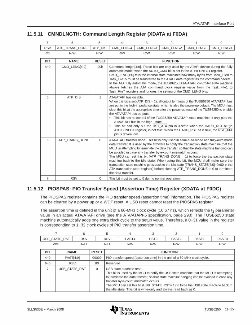
ATA/ATAPI Interface Port
11−15SLLS535E − March 2008 TUSB6250
11.5.11 CMNDLNGTH: Command Length Register (XDATA at F0DA)
7 6 5 4 3 2 1 0
RSV ATP_TRANS_DONE ATP_DIS CMD_LENG4 CMD_LENG3 CMD_LENG2 CMD_LENG1 CMD_LENG0
R/O R/W R/W R/W R/W R/W R/W R/W
BIT NAME RESET FUNCTION
4−0 CMD_LENG[4:0] 00h Command length[4:0]. These bits are only used by the ATAPI device during the fullyautomatic mode, when the AUTO_CMD bit is set in the ATPIFCNFG1 register.CMD_LENG[4:0] tells the internal state machines how many bytes from Task_File0 toTask_File15 must be transferred to the ATAPI data register as the command packet.In the ATA fully automatic mode, the TUSB6250 ATA/ATAPI controller state machinealways fetches the ATA command block register value from the Task_File1 toTask_File7 registers and ignores the setting of the CMD_LENG bits.
5 ATP_DIS 1 ATA/ATAPI bus disable.When this bit is set (ATP_DIS = 1), all output terminals of the TUSB6250 ATA/ATAPI busare put in the high-impedance state, which is also the power-up default. The MCU mustclear this bit at the appropriate time after the power-up reset of the TUSB6250 to enablethe ATA/ATAPI bus outputs. This bit has no control of the TUSB6250 ATA/ATAPI state machine. It only puts the
ATA/ATAPI bus in the high--state. This bit can only put the RST_ATA pin in 3-state when the HARD_RST bit (in
ATPIFCNFG1 register) is not true. When the HARD_RST bit is true, the RST_ATApin is driven low.
6 ATP_TRANS_DONE 0 ATA/ATAPI transfer done. This bit is only used in semi-auto mode and fully-auto modedata transfer. It is used by the firmware to notify the transaction state machine that theMCU isi attempting to terminate the data transfer, so that the state machine hanging canbe avoided in case any transfer byte-count mismatch occurs.The MCU can set this bit (ATP_TRANS_DONE = 1) to force the transaction statemachine back to the idle state. When using this bit, the MCU shall make sure thetransaction state machine goes back to the idle state (TRANS_STATE[4:0]=0x00 in theATA transaction state register) before clearing ATP_TRANS_DONE to 0 to terminatethe data transfer.
7 RSV 0 This bit must be set to 0 during normal operation.
11.5.12 PIOSPAS: PIO Transfer Speed (Assertion Time) Register (XDATA at F0DC)
The PIOSPAS register contains the PIO transfer speed (assertion time) information. The PIOSPAS registercan be cleared by a power up or a WDT reset. A USB reset cannot reset the PIOSPAS register.
The assertion time is defined in the unit of a 60-MHz clock cycle (16.67 ns), which reflects the t2 parametervalue in an actual ATA/ATAPI drive (see the ATA/ATAPI-5 specification, page 293). The TUSB6250 statemachine automatically adds one extra clock cycle to the setup value. Therefore, a 0−31 value in the registeris corresponding to 1−32 clock cycles of PIO transfer assertion time.
7 6 5 4 3 2 1 0
USB_STATE_RST RSV RSV PAST4 PST3 PAST2 PAST1 PAST0
W/O R/O R/O R/W R/W R/W R/W R/W
BIT NAME RESET FUNCTION
4−0 PAST[4:0] 00000 PIO transfer speed (assertion time) in the unit of a 60-MHz clock cycle.
6−5 RSV 00 Reserved
7 USB_STATE_RST 0 USB state machine reset.This bit is used by the MCU to notify the USB state machine that the MCU is attemptingto terminate the data transfer, so that state machine hanging can be avoided in case anytransfer byte-count mismatch occurs.The MCU can set this bit (USB_STATE_RST= 1) to force the USB state machine back tothe idle state. This bit is write-only and always read back as 0.
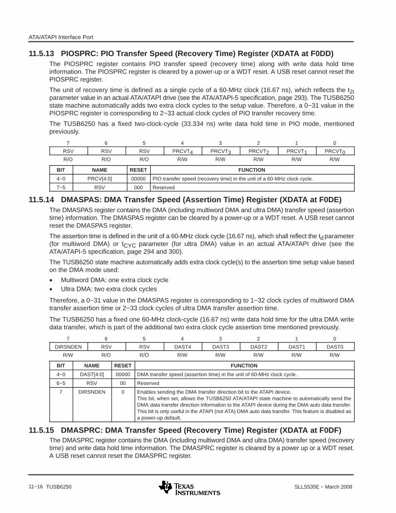
ATA/ATAPI Interface Port
11−16 SLLS535E − March 2008TUSB6250
11.5.13 PIOSPRC: PIO Transfer Speed (Recovery Time) Register (XDATA at F0DD)The PIOSPRC register contains PIO transfer speed (recovery time) along with write data hold timeinformation. The PIOSPRC register is cleared by a power-up or a WDT reset. A USB reset cannot reset thePIOSPRC register.
The unit of recovery time is defined as a single cycle of a 60-MHz clock (16.67 ns), which reflects the t2iparameter value in an actual ATA/ATAPI drive (see the ATA/ATAPI-5 specification, page 293). The TUSB6250state machine automatically adds two extra clock cycles to the setup value. Therefore, a 0−31 value in thePIOSPRC register is corresponding to 2−33 actual clock cycles of PIO transfer recovery time.
The TUSB6250 has a fixed two-clock-cycle (33.334 ns) write data hold time in PIO mode, mentionedpreviously.
7 6 5 4 3 2 1 0
RSV RSV RSV PRCVT4 PRCVT3 PRCVT2 PRCVT1 PRCVT0R/O R/O R/O R/W R/W R/W R/W R/W
BIT NAME RESET FUNCTION
4−0 PRCV[4:0] 00000 PIO transfer speed (recovery time) in the unit of a 60-MHz clock cycle.
7−5 RSV 000 Reserved
11.5.14 DMASPAS: DMA Transfer Speed (Assertion Time) Register (XDATA at F0DE)The DMASPAS register contains the DMA (including multiword DMA and ultra DMA) transfer speed (assertiontime) information. The DMASPAS register can be cleared by a power-up or a WDT reset. A USB reset cannotreset the DMASPAS register.
The assertion time is defined in the unit of a 60-MHz clock cycle (16.67 ns), which shall reflect the td parameter(for multiword DMA) or tCYC parameter (for ultra DMA) value in an actual ATA/ATAPI drive (see theATA/ATAPI-5 specification, page 294 and 300).
The TUSB6250 state machine automatically adds extra clock cycle(s) to the assertion time setup value basedon the DMA mode used:
• Multiword DMA: one extra clock cycle• Ultra DMA: two extra clock cycles
Therefore, a 0−31 value in the DMASPAS register is corresponding to 1−32 clock cycles of multiword DMAtransfer assertion time or 2−33 clock cycles of ultra DMA transfer assertion time.
The TUSB6250 has a fixed one 60-MHz clock-cycle (16.67 ns) write data hold time for the ultra DMA writedata transfer, which is part of the additional two extra clock cycle assertion time mentioned previously.
7 6 5 4 3 2 1 0
DIRSNDEN RSV RSV DAST4 DAST3 DAST2 DAST1 DAST0
R/W R/O R/O R/W R/W R/W R/W R/W
BIT NAME RESET FUNCTION
4−0 DAST[4:0] 00000 DMA transfer speed (assertion time) in the unit of 60-MHz clock cycle.
6−5 RSV 00 Reserved
7 DIRSNDEN 0 Enables sending the DMA transfer direction bit to the ATAPI device.This bit, when set, allows the TUSB6250 ATA/ATAPI state machine to automatically send theDMA data transfer direction information to the ATAPI device during the DMA auto data transfer.This bit is only useful in the ATAPI (not ATA) DMA auto data transfer. This feature is disabled asa power-up default.
11.5.15 DMASPRC: DMA Transfer Speed (Recovery Time) Register (XDATA at F0DF)The DMASPRC register contains the DMA (including multiword DMA and ultra DMA) transfer speed (recoverytime) and write data hold time information. The DMASPRC register is cleared by a power up or a WDT reset.A USB reset cannot reset the DMASPRC register.

ATA/ATAPI Interface Port
11−17SLLS535E − March 2008 TUSB6250
The unit of recovery time is defined as a single cycle of a 60-MHz clock (16.67 ns), which reflects the tKparameter (for multiword DMA) or tRP parameter (for ultra DMA) value in an actual ATA/ATAPI drive (see theATA/ATAPI-5 specification, pages 294 and 300).
The TUSB6250 state machine automatically adds extra clock cycle(s) to the recovery time setup value basedon the DMA mode used:
• Multiword DMA: two extra clock cycles• Ultra DMA: one extra clock cycle
Therefore, a 0−31 value in the DMASPRC register corresponds to 2−33 clock cycles of multiword DMAtransfer recovery time or 1−32 clock cycles of ultra DMA transfer recovery time.
The TUSB6250 has a fixed two 60-MHz clock cycle (33.34 ns) write data hold time for multiword DMA writedata transfer, which is part of the additional two extra clock cycle recovery time mentioned above.
7 6 5 4 3 2 1 0
RSV RSV RSV DRCVT4 DRCVT3 DRCVT2 DRCVT1 DRCVT0
R/O R/O R/O R/W R/W R/W R/W R/W
BIT NAME RESET FUNCTION
4−0 DRCVT[4:0] 00000 DMA transfer speed (recovery time) in the unit of 60-MHz clock cycle.
7−5 RSV 000 Reserved
11.5.16 Data Transfer Mode and Timing Reference ChartThe TUSB6250 firmware builds a default lookup table based on the correlation data between the data transfermodes and their corresponding timing given in Table 11−4 through Table 11−6. It should be noted that theassertion and recovery times given here do not reflect the actual performance of the TUSB6250 ATA/ATAPIdata transfer engine. The intention of listing these times is to provide a set of timing values that complies withthe ATA/ATAPI-5 specification requirement. End-product vendors can develop their custom firmware withdifferent timing settings to be adapted to the actual performance of their drive. The timing below is based onthe 60-MHz clock (using 16 ns as a typical clock-cycle period) that the ATA/ATAPI controller state machineis running.
Table 11−4. PIO Mode and Timing Correlation ChartCYCLE TIME (t0) ASSERTION TIME (t2) RECOVERY TIME (t2I)
PIOTRANSFER
MODE
TIME(ns)
TIME(ns)
# OF CLKS (SEENOTE 1)
TIME(ns)
# OF CLKS (SEENOTE 1)TRANSFER
MODE SPEC(MIN) ACTUAL
SPEC(MIN) ACTUAL
REGISTERSETTING ACTUAL
SPEC(MIN) ACTUAL
REGISTERSETTING ACTUAL
0 600 600.12 290 300.06 17 18 N/A 300.06 16 18
1 383 383.41 290 300.06 17 18 N/A 83.35 3 5
2 330 333.4 290 300.06 17 18 N/A 33.34 0 2
3 180 183.37 80 83.35 4 5 70 100.02 4 6
4 120 133.36 70 83.35 4 5 25 50.01 1 3
Other N/A 600.12 N/A 300.06 17 18 N/A 300.06 16 18
NOTES: 1. All the actual timing listed is based on the 60-MHz clock cycle (16.67 ns) used in the TUSB6250.• The spec value listed is based on the ATA/ATAPI-5 specification.• The actual assertion time is obtained based on the consideration that both the register and data transfer timings must be met.• The actual recovery time is obtained with the consideration to meet both the cycle time and the recovery time value specified in the
ATA/ATAPI-5 specification, after meeting the assertion time.• Because the TUSB6250 hardware always adds one extra clock cycle to the assertion time value and two extra clock cycles to the
recovery time value, the TUSB6250 firmware must use one less than the desired number of clock cycles for any assertion time andtwo less for any recovery time programming value. For example, to achieve 300.06-ns assertion and recovery time for PIO mode0, instead of using 18 clock cycles as the assertion and recovery time value, the TUSB6250 firmware must use only 17 clock cyclesas assertion time and 16 clock cycles as the recovery time programming value.
• According to the ATA/ATAPI-5 specification, the TUSB6250 firmware can issue an IDENTIFY DEVICE command to determine thesupported modes of the mass storage device and then use the corresponding timing in this table during the data transfer.

ATA/ATAPI Interface Port
11−18 SLLS535E − March 2008TUSB6250
Table 11−5. Multiword DMA Mode and Timing Correlation ChartCYCLE TIME (t0) ASSERTION TIME (tD) RECOVERY TIME (tK)
MWDMATRANSFER
MODE
TIME(ns)
TIME(ns)
# OF CLKS (SEENOTE 1)
TIME(ns)
# OF CLKS (SEENOTE 1)TRANSFER
MODE SPEC(MIN) ACTUAL
SPEC(MIN) ACTUAL
REGISTERSETTING ACTUAL
SPEC(MIN) ACTUAL
REGISTERSETTING ACTUAL
0 480 483.43 215 216.71 12 13 250 266.72 14 16
1 150 150.03 80 83.35 4 5 50 66.68 2 4
2 120 133.36 70 83.35 4 5 25 50.01 1 3
Other N/A 483.43 N/A 216.71 12 13 N/A 266.72 14 16
NOTES: 1. All the actual timing listed is based on the 60-MHz clock cycle (16.67 ns) used in the TUSB6050.• The spec value listed is based on the ATA/ATAPI-5 specification.• The actual recovery time is obtained with the consideration to meet both the cycle time and recovery time value specified in the
ATA/ATAPI-5 specification, after meeting the assertion time.• Because the TUSB6250 hardware always adds one extra clock cycle to the assertion time value and two extra clock cycles to the
recovery time value, the TUSB6250 firmware must use one less than the desired number of clock cycles for any assertion time andtwo less for any recovery time programming value. For example, to achieve 216.71-ns assertion and a 266.72-ns recovery time forMWDMA mode 0, instead of using 13 clock cycles as the assertion and 16 clock cylces as the recovery time value, the firmwaremust use only 12 clock cycles as assertion time and 14 clock cycles as the recovery time programming value.
• According to the ATA/ATAPI-5 specification, the TUSB6250 firmware can issue an IDENTIFY DEVICE command to determine thesupported modes of the mass storage device and then use the corresponding timing in this table during the data transfer.
Table 11−6. Ultra DMA Mode and Timing Correlation Chart (Applies to UDMA Write Only)CYCLE TIME ASSERTION TIME (tCYC) RECOVERY TIME (tRP)
UDMATRANSFER
TIME(ns)
TIME(ns)
# OF CLKS (SEENOTE 1)
TIME(ns)
# OF CLKS (SEENOTE 1)
TRANSFERMODE SPEC
(MIN) ACTUALSPEC(MIN) ACTUAL
REGISTERSETTING ACTUAL
SPEC(MIN) ACTUAL
REGISTERSETTING
ACTUAL(SEE
NOTE 4)
0 224 233.38 112 116.69 5 7 160 166.7 9 10
1 146 166.7 73 83.35 3 5 125 133.36 7 8
2 108 133.36 54 66.68 2 4 100 100.02 5 6
3 78 100.02 39 50.01 1 3 100 100.02 5 6
4 50 66.68 25 33.34 0 2 100 100.02 5 6
Other N/A 233.38 N/A 116.69 5 7 N/A 166.7 9 10
NOTES: 1. All the actual timing listed is based on the 60-MHz clock cycle (16.67 ns) used in the TUSB6050.• The spec value listed is based on the ATA/ATAPI-5 specification.• ATA/ATAPI-5 specification does not define cycle time for UDMA data transfer. The cycle time is used here for easy comparison with
PIO and MWDMA mode, which equals twice the assertion time.• The actual recovery time tRP has an actual overhead of one to three clock cycles. What is listed in this table is the minimum value.
It should be noted that the recovery time has no contribution to the cycle time in the UDMA data transfer, because it only affects thetiming when pausing a UDMA data transfer.
• The firmware must use two less clock cycles than the desired number of clock cycles for the assertion time and one less clock cyclesfor the recovery time programming value.

ATA/ATAPI Interface Port
11−19SLLS535E − March 2008 TUSB6250
11.6 ATA/ATAPI Group 2 RegistersTable 11−7. Group 2 Registers
MMR ADDRESSOFFSET ADDRESS
(BASE ADDRESS = F0C0) REGISTER DESCRIPTION
F0E0 20h MCU data Byte_0 register
F0E1 21h MCU data Byte_1 register
F0E2 22h MCU data Byte_2 register
F0E3 23h MCU data Byte_3 register
F0E4 24h MCU access address low-byte register
F0E5 25h MCU access address high-byte register
F0E6 26h ATA/ATAPI interrupt register 0
F0E7 27h ATA/ATAPI interrupt mask register 0
F0E8 28h ATA/ATAPI interrupt register 1
F0E9 29h ATA/ATAPI interrupt mask register 1
F0EA 2Ah ATA/ATAPI interface status register
F0EB 2Bh Sector FIFO write pointer low-byte register
F0EC 2Ch Sector FIFO write pointer high-byte register
F0ED 2Dh Sector FIFO write pointer backup low-byte register
F0EE 2Eh Sector FIFO write pointer backup high-byte register
F0EF 2Fh Sector FIFO read pointer low-byte register
F0F0 30h Sector FIFO read pointer high-byte register
F0F1 31h Sector FIFO read pointer backup low-byte register
F0F2 32h Sector FIFO read pointer backup high-byte register
F0F9 39h Ultra receive extra word count
The MCU can access the sector FIFO memory indirectly by using the MCU access address low/high registers(MCUACSL and MCUACSH) and the MCU data registers (MCUBYTE[0:3]). The access address and directionmust be set before the data access can occur. The write and read sequences are described in detail as follows.
MCU Write to Sector FIFO Memory:
1. The MCU writes to the MCU access address low-byte register (MCUACSL), then to the MCU accessaddress high-byte register (MCUACSH) to set up the start address in MACS_ADR[12:0], and setMACS_DIR to 0.
2. The MCU writes to the MCU data Byte_0 register (MCUBYTE0), MCU data Byte_1 register (MCUBYTE1),MCU data Byte_2 register (MCUBYTE2), MCU data Byte_3 register (MCUBYTE3), in this fixed order.After the MCU finishes the write to the MCU data Byte_3 register (MCUBYTE3), the internal logic writesthe complete 32-bit data into the sector FIFO location with the address pointed to by MACS_ADR[12:0]and sets MACS_BUSY to 1.
3. After the internal logic finishes the write of 32-bit data into sector FIFO, it clears MACS_BUSY to 0, andincrements MACS_ADR[12:0] by 1.
4. The MCU continues steps 2 and 3 to write the next 32-bit data into sector FIFO for consecutive writes,until the MCU writes to the MCU access address register with a new address.
MCU Read to Sector FIFO Memory:
1. The MCU writes to the MCU access address low-byte register (MCUACSL) and then to the MCU accessaddress high-byte register (MCUACSH) to set up the start address in MACS_ADR[12:0] and setMACS_DIR to 1.
2. After the MCU finishes the write to the MCU access address high-byte register (MCUACSH), the internallogic prefetches the 32-bit data from sector FIFO memory pointed to by MACS_ADR[12:0] and sets

ATA/ATAPI Interface Port
11−20 SLLS535E − March 2008TUSB6250
MACS_BUSY to 1. When the internal logic reads from the sector FIFO memory, it loads the 32-bit datainto the MCU data Byte_3 register (MCUBYTE3), MCU data Byte_2 register (MCUBYTE2), MCU dataByte_1 register (MCUBYTE1), MCU data Byte_0 register (MCUBYTE0), clears MACS_BUSY to 0, andincrements MACS_ADR[12:0] by 1.
3. The MCU reads the MCU data Byte_0 register (MCUBYTE0), MCU data Byte_1 register (MCUBYTE1),MCU data Byte_2 register (MCUBYTE2), and the MCU data Byte_3 register (MCUBYTE3) in this fixedorder.
4. After the MCU finishes the read from the MCU data Byte_3 register, the internal logic prefetches the next32-bit data from sector FIFO pointed to by the current MACS_ADR[12:0]. The same sequence asdescribed in Steps 2 and 3 is followed for consecutive reads until the MCU writes to the MCU accessaddress register with a new address.
5. Noted that although the MCU is allowed to read part of the 32-bit read data, it must ensure that the lastread goes to the MCU data Byte_3 register (MCUBYTE3). This serves as an indication to the TUSB6250internal logic that the MCU has finished the read process to the current 32-bit read data and is ready tolet the internal logic fetch the next 32-bit data. Without the read from the MCUBYTE3 register, the internallogic does not perform prefetch of the next 32-bit data.
11.6.1 MCUBYTE0: MCU Data Byte_0 Register (XDATA at F0E0)
7 6 5 4 3 2 1 0
MACS_DB07 MACS_DB06 MACS_DB05 MACS_DB04 MACS_DB03 MACS_DB02 MACS_DB01 MACS_DB00
R/W R/W R/W R/W R/W R/W R/W R/W
BIT NAME RESET FUNCTION
7−0 MACS_DB0[7:0] 00h This register contains the sector FIFO memory data buffer byte 0 accessible by the MCU.
11.6.2 MCUBYTE1: MCU Data Byte_1 Register (XDATA at F0E1)
7 6 5 4 3 2 1 0
MACS_DB17 MACS_DB16 MACS_DB15 MACS_DB14 MACS_DB13 MACS_DB12 MACS_DB11 MACS_DB10
R/W R/W R/W R/W R/W R/W R/W R/W
BIT NAME RESET FUNCTION
7−0 MACS_DB1[7:0] 00h This register contains the sector FIFO memory data buffer byte 1 accessible by the MCU.
11.6.3 MCUBYTE2: MCU Data Byte_2 Register (XDATA at F0E2)
7 6 5 4 3 2 1 0
MACS_DB27 MACS_DB26 MACS_DB25 MACS_DB24 MACS_DB23 MACS_DB22 MACS_DB21 MACS_DB20
R/W R/W R/W R/W R/W R/W R/W R/W
BIT NAME RESET FUNCTION
7−0 MACS_DB2[7:0] 00h This register contains the sector FIFO memory data buffer byte 2 accessible by the MCU.
11.6.4 MCUBYTE3: MCU Data Byte_3 Register (XDATA at F0E3)
7 6 5 4 3 2 1 0
MACS_DB37 MACS_DB36 MACS_DB35 MACS_DB34 MACS_DB33 MACS_DB32 MACS_DB31 MACS_DB30
R/W R/W R/W R/W R/W R/W R/W R/W
BIT NAME RESET FUNCTION
7−0 MACS_DB3[7:0] 00h This register contains the sector FIFO memory data buffer byte 3 accessible by the MCU.

ATA/ATAPI Interface Port
11−21SLLS535E − March 2008 TUSB6250
11.6.5 MCUACSL: MCU Access Address Low-Byte Register (XDATA at F0E4)
7 6 5 4 3 2 1 0
MACS_ADR7 MACS_ADR6 MACS_ADR5 MACS_ADR4 MACS_ADR3 MACS_ADR2 MACS_ADR1 MACS_ADR0
R/W R/W R/W R/W R/W R/W R/W R/W
BIT NAME RESET FUNCTION
7−0 MACS_ADR[7:0] 00h MCU access address[7:0]. These bits contain the MCU access sector FIFO memory addresslower 8 bits.
11.6.6 MCUACSH: MCU Access Address High-Byte Register (XDATA at F0E5)7 6 5 4 3 2 1 0
MACS_DIR MACS_BUSY RSV MACS_ADR12 MACS_ADR11 MACS_ADR10 MACS_ADR9 MACS_ADR8
R/W R/O R/O R/W R/W R/W R/W R/W
BIT NAME RESET FUNCTION
4−0 MACS_ADR[12:8] 00000 MCU access address[12:8]. These bits contain the MCU access sector FIFOmemory address higher 5 bits.
5 RSV 0 Reserved
6 MACS_BUSY 0 MCU access busy. Read-only.This bit, when set, indicates the internal logic is busy prefetching the next 32-bitread data or writing the 32-bit data to the sector FIFO memory from the MCU databyte 0−3 registers.
7 MACS_DIR 0 MCU access direction. If MACS_DIR = 0, MCU is going to write data to sector FIFO memory. If MACS_DIR = 1, MCU is going to read data from sector FIFO memory.When the MCU sets MACS_DIR to 1 by first writing to the MCU access addresshigh-byte register, the internal logic prefetches the read data pointed byMACS_ADR[12:0], stores the read data in the MCU data byte 0−3 registers, andincrements MACS_ADR[12:0] by 1.
11.6.7 ATPINTRPT0: ATA/ATAPI Interrupt Register 0 and ATPINTMSK0: ATA/ATAPIInterrupt Mask Register 0 (XDATA at F0E6, F0E7)
This register set includes the ATA/ATAPI interrupt register 0 (allocated at the MMR address 0xF0E6) and theATA/ATAPI interrupt mask register 0 (allocated at the MMR address 0xF0E7).
The ATA/ATAPI interrupt register 0 provides the source information of the interrupt. The MCU can read thisregister to determine the source of a pending interrupt, if any. To clear a particular interrupt, the MCU mustwrite a 1 to the corresponding bit to clear it to 0. There is another way to clear the USB_XFR_DN andATP_XFR_DN interrupts, which is automatically cleared to 0 when the firmware sets the START_ATAPI bitin the ATPIFCNFG1 register to begin a data transfer.
7 6 5 4 3 2 1 0
ATP_COMP ATP_ER ATP_XFR_DN USB_XFR_PEND USB_XFR_DN ATP_BYTECN_MIS ATPINT1_PEND ATP_INT
R/W R/W R/W R/W R/W R/W R/O R/W
BIT NAME RESET FUNCTION
0 ATP_INT 0 ATAPI interrupt. This bit indicates that an interrupt has occurred at the ATA/ATAPIinterface. ATP_INT is set only during the manual phase of a sequence. During the automatic phase of a sequence, the hardware handles ATA INTRQ
automatically without the MCU intervention.
1 ATPINT1_PEND 0 Interrupt pending in ATPINTRPT1.This bit, when set, indicates that in addition to the interrupt source indicated in this register(ATPINTRPT0), there is also some other interrupt source for the current pending ATAinterrupt (vector value = 0x48) reflected in the vector interrupt register.

ATA/ATAPI Interface Port
11−22 SLLS535E − March 2008TUSB6250
2 ATP_BYTECN_MIS 0 ATA/ATAPI byte-count mismatch.This bit, when set, indicates that there is a byte-count mismatch that occurred for thecurrent data transfer at the ATA/ATAPI interface. The MCU is responsible for reading theATA/ATAPI interface status register or transfer byte-count register to determine the actualevent causing the mismatch.
3 USB_XFR_DN 0 USB transfer done.This bit, when set, indicates the data transfer is finished at the USB interface side, whichdoes not mean the transfer ended free of error. The MCU is responsible for checkingwhether any byte-count mismatch occurred.
4 USB_XFR_PEND 0 USB transfer pending.This bit, when set, indicates the data transfer at the USB interface side is not finished anda byte-count mismatch or other error condition is pending. The MCU must check the otherregisters to determine the exact error that occurred. Before clearing this interrupt, theMCU must ensure the USBWPNABRTEN bit is set correctly, so that the state machine caneither flush or send the data in the sector FIFO to the ATAPI device.
5 ATP_XFR_DN ATA/ATAPI transfer done.This bit, when set, indicates the data transfer is finished at the ATA/ATAPI interface side,which does not mean the transfer ended free of error. The MCU is responsible for checkingwhether any byte-count mismatch occurred.
6 ATP_ER 0 ATA/ATAPI error.This bit, when set, indicates an error occurred during the ATA/ATAPI autocommandsequence. The MCU must read the Taks_File registers to determine the cause of the error.
7 ATP_COMP 0 ATA/ATAPI normal completion.This bit, when set, indicates the command execution is finished without any error.When ATP_COMP is set, the MCU must write a 1 to clear it back to 0.
NOTES: 1. Most of the interrupt sources indicated in this register, except the ATP_INT bit, reflect the ATA interrupt with the vectorinterrupt value of 0x48.
2. The interrupt sources indicated in the ATA interrupt are the most common. For other interrupt sources that happen lessfrequently, the ATPINT1_PEND bit provides an easy indication to the MCU whether any of them occurred for the currentpending interrupt as indicated in the ATPINTRPT1 register.
3. The ATA interrupt mask register 0 is the interrupt enable register that can be read and written by the MCU. To enable aparticular interrupt, the MCU must write a 1 to the corresponding bit.
11.6.8 ATPINTRPT1: ATA/ATAPI Interrupt Register 1 and ATPINTMSK1: ATA/ATAPIInterrupt Mask Register 1 (XDATA at F0E8, F0E9)
This register set includes two registers: the ATA/ATAPI interrupt register 1 (allocated at MMR address 0xF0E8)and the ATA/ATAPI interrupt mask register 1 (allocated at MMR address 0xF0E9). See the notes in Section11.6.7, ATPINTRPT0: ATA/ATAPI Interrupt Register 0 and ATPINTMSK0: ATA/ATAPI Interrupt Mask Register0 (XDATA at F0E6, F0E7), for the related information.
7 6 5 4 3 2 1 0
RSV RSV RSV RSV ATP_BSY ATP_SEQ_ER ATP_DSEQ_ER ATP_NDA_CMD
R/O R/O R/O R/O R/W R/W R/W R/W
BIT NAME RESET FUNCTION
0 ATP_NDA_CMD 0 ATA nondata command mismatch.This bit, when set, indicates that: A nondata command is specified in the ATA/ATAPI interface configuration register 1. When the command is issued, the ATA/ATAPI device indicates the data transfer operation
is currently active.
1 ATP_DSEQ_ER 0 ATAPI data sequence error.In the ATAPI mode, this bit indicates there is a sequence error that occurred during datatransfer. The MCU must read the interrupt reason register and byte-count register (both in thestorage device) to determine the cause of the error.
2 ATP_SEQ_ER 0 ATAPI sequence error.In the ATAPI mode with full autosequencing, this bit indicates that a sequence error hasoccurred after writing a packet command (command code A0h), but before the commandpacket bytes have been issued.The MCU must read the ATAPI interrupt reason register to determine the cause of the error.

ATA/ATAPI Interface Port
11−23SLLS535E − March 2008 TUSB6250
3 ATP_BSY 0 ATA/ATAPI busy.This bit, when set, indicates the ATA/ATAPI device is busy at the start of the command (afterwriting START_ATAPI). The command is not executed in the autocommand mode.The MCU must read the Task_File registers to determine why the ATA/ATAPI device is busy.
7−4 RSV 0h Reserved
11.6.9 ATPSTATUS: ATA/ATAPI Interface Status Register (XDATA at F0EA)The ATPSTATUS register provides some status information on the ATA/ATAPI interface. Bit 0 indicates theATA/ATAPI device overrun condition. Bits 3–1 mirror the real-time logic level on the DMARQ, DMACK, andINTRQ pins.
7 6 5 4 3 2 1 0
RSV ULTRARCV_EX SYNBUF_RCVERR BUFOVFLOW INTRQ DMACK DMARQ ATP_OVRUN
R/O R/O R/O R/O R/O R/O R/O R/C
BIT NAME RESET FUNCTION
0 ATP_OVRUN 0 ATA/ATAPI device overrun.This bit, when set, indicates that the ATA/ATAPI device attempts to process more data thanthe USB host expected (dCBWDataTransferLength in the USB mass storage bulk-onlyspec). This bit reflects the H < D cases defined by the Universal Serial Bus Mass StorageClass Bulk-Only Transport specification. It should be noted that when ATP_OVRUN occurs, the ATP_BYTECN_MIS interrupt is
triggered. However, the transfer byte-count register may have a zero value to indicate theTUSB6250 moved H number of bytes, as expected by the USB host.
In the PIO auto-data transfer mode, INTRQ may be set when a device-overrun conditionoccurs. If reading the ATAPI status register returns DRQ=1, the ATP_OVRUN bit is setto reflect the condition that the device attempts to process more data than expected.
In the DMA/UDMA auto-data transfer mode (UDMA read), when a device-overruncondition occurs, the TUSB6250 pauses and tries to stop the current UDMA-readtransfer. The ATP_OVRUN bit is not set if INTRQ is asserted thereafter. It is set only whenINTRQ is not asserted; however DMARQ is asserted again.
This bit can be cleared by either writing a 1 to this bit or setting the START_ATAPI bit in theATAIFCNFG1 register.
1 DMARQ 0 DMARQ status bit.This bit mirrors the real-time status on the DMARQ pin.
2 DMACK 0 DMACK status bit.This bit mirrors the real-time status on the DMACK pin.
3 INTRQ 0 INTRQ status bit.This bit mirrors the real-time status on the INTRQ pin.

ATA/ATAPI Interface Port
11−24 SLLS535E − March 2008TUSB6250
BIT FUNCTIONRESETNAME
4 BUFOVFLOW 0 Internal buffer overflow error.
The internal buffer refers to the 6-byte internal buffer space outside of sector FIFO designedto handle extra data that may be received from the ATA/ATAPI device in pausing a UDMAread operation.
This bit, when set, indicates that the 6-byte internal data buffer experienced overflow (morethan 6 bytes of data are transferred into this 6-byte internal buffer space after either sectorFIFO full or expected transfer byte count is reached for current auto-data transfer).
This bit can be used in all nonmanual data transfer modes, which include both read and writedata transfers. It may be useful in UDMA-read data transfer as error indication. For PIO ormultiword DMA data transfer, BUFOVFLOW should not happen, unless a hardware logicerror occurred. In such case, this bit is useful for debugging.
For a read transfer, the BUFOVFLOW could happen when the following cases occur:
The sector FIFO is full, however the expected byte count has not been reached yet.
For a write transfer, the BUFOVFLOW can only happen in a hardware logic error condition:
The TUSB6250 is sending the data normally to the ATA/ATAPI device; however, a deviceerror causes it to pause and terminate the current data transfer. This bit is set if a hardwarelogic error occurs, such that the TUSB6250 ATA/ATAPI state machine doesn’t respondto the ATA/ATAPI device’s pause and termination request. This bit is useful to debug thisrare case.
The MCU can set either the SOFT_RST bit or the START_ATAPI bit in the ATA/ATAPIinterface configuration register to 1 to clear the BUFOVFLOW bit.
5 SYNBUF_RCVERR 0 Ultra DMA receive synch-buffer error (for UDMA-read-only)
This bit, when set, indicates that the synch buffer for the ultra DMA receive operation has anoverrun error. This error may occur when the ATA/ATAPI device bursts data at a transfer ratefaster than 120 MBps.
The MCU can set either the SOFT_RST bit or the START_ATAPI bit in the ATA/ATAPIinterface configuration register 1 to clear the SYNBUF_RCVERR bit.
6 ULTRA_RCVEX 0 Ultra DMA receive extra (for UDMA-read-only).
This bit, when set, indicates several extra bytes of data were received after the TUSB6250received the expected number of bytes from the ATA/ATAPI device. These extra bytes arereceived at the time period between the TUSB6250 pausing and terminating a UDMA readtransfer. The exact word (2-byte) count for this data is stored in the ULRCVEXCNT register.
It should be noted that the extra number of bytes received are discarded right away, becausethe TUSB6250 already received the expected number of bytes. However, the TUSB6250continues to calculate CRC for all the extra data received until the TUSB6250 terminates theUDMA read transfer. The ATA/ATAPI device, which sent more data than expected, butstopped sending data after the TUSB6250 terminates the UDMA read transfer, does notreceive any CRC error from the TUSB6250.
7 RSV 0 Reserved
11.6.10 SECWRPTL: Sector FIFO Write Pointer Low-Byte Register (XDATA at F0EB)
7 6 5 4 3 2 1 0
WR_PTR7 WR_PTR6 WR_PTR5 WR_PTR4 WR_PTR3 WR_PTR2 WR_PTR1 WR_PTR0
R/O R/O R/O R/O R/O R/O R/O R/O
BIT NAME RESET FUNCTION
7−0 WR_PTR[7:0] 00h This register contains the sector FIFO write pointer lower 8-bit value. Read-only

ATA/ATAPI Interface Port
11−25SLLS535E − March 2008 TUSB6250
11.6.11 SECWRPTH: Sector FIFO Write Pointer High-Byte Register (XDATA at F0EC)
7 6 5 4 3 2 1 0
SEC_FIFO_EMPT RSV WR_PTR13 WR_PTR12 WR_PTR11 WR_PTR10 WR_PTR9 WR_PTR8
R/O R/O R/O R/O R/O R/O R/O R/O
BIT NAME RESET FUNCTION
5−0 WR_PTR[13:8] 000000 These bits contain the sector FIFO write pointer higher 6-bit value. Read-onlyWR_PTR[13:0] is used as the current write pointer to write data into sector FIFO. The writedata is temporarily invisible to the read side until the data is confirmed. When the UBM writesthe received data from the USB to the sector FIFO and CRC error occurs, the UBM aborts thewritten data, then WR_PTR_BK[13:0] is copied back into WR_PTR[13:0] to resetWR_PTR[13:0] back to the location before the write.
6 RSV 0 Reserved
7 SEC_FIFO_EMPT 0 Sector FIFO empty. Read-onlyThis bit, when set, indicates the sector FIFO is empty.Before executing any command with data transfer, the MCU must ensure theSEC_FIFO_EMPT bit is set. If it is not set due to error from a previous command, the MCUmust set the CLR_SECFIFO bit (bit 1 of the ATA/ATAPI access register 2) to completely emptythe sector FIFO.
11.6.12 WRPTBKUPL: Sector FIFO Write Pointer Backup Low-Byte Register (XDATA atF0ED)
7 6 5 4 3 2 1 0
WR_PTR_BK7 WR_PTR_BK6 WR_PTR_BK5 WR_PTR_BK4 WR_PTR_BK3 WR_PTR_BK2 WR_PTR_BK1 WR_PTR_BK0
R/O R/O R/O R/O R/O R/O R/O R/O
BIT NAME RESET FUNCTION
7−0 WR_PTR_BK[7:0] 00h This register contains the confirmed sector FIFO write pointer lower 8-bit value. Read-only
11.6.13 WRPTBKUPH: Sector FIFO Write Pointer Backup High-Byte Register (XDATA atF0EE)
7 6 5 4 3 2 1 0
RSV RSV WR_PTR_BK13 WR_PTR_BK12 WR_PTR_BK11 WR_PTR_BK10 WR_PTR_BK9 WR_PTR_BK8
R/O R/O R/O R/O R/O R/O R/O R/O
BIT NAME RESET FUNCTION
5−0 WR_PTR_BK[13:8] 000000 These bits contain the confirmed sector FIFO write pointer higher 6-bit value. Read-only.When the write data is confirmed, WR_PTR[13:0] is copied into WR_PTR_BK[13:0]. The readside of the sector FIFO can only read the data up to the location pointed to byWR_PTR_BK[13:0].
7−6 RSV 00 Reserved
11.6.14 SECRDPTL: Sector FIFO Read Pointer Low-Byte Register (XDATA at F0EF)
7 6 5 4 3 2 1 0
RD_PTR7 RD_PTR6 RD_PTR5 RD_PTR4 RD_PTR3 RD_PTR2 RD_PTR1 RD_PTR0
R/O R/O R/O R/O R/O R/O R/O R/O
BIT NAME RESET FUNCTION
7−0 RD_PTR[7:0] 00h This register contains the sector FIFO write pointer lower 8-bit value. Read-only

ATA/ATAPI Interface Port
11−26 SLLS535E − March 2008TUSB6250
11.6.15 SECRDPTH: Sector FIFO Read Pointer High-Byte Register (XDATA at F0F0)
7 6 5 4 3 2 1 0
RSV RSV RD_PTR13 RD_PTR12 RD_PTR11 RD_PTR10 RD_PTR9 RD_PTR8
R/O R/O R/O R/O R/O R/O R/O R/O
BIT NAME RESET FUNCTION
5−0 RD_PTR[13:8] 000000 These bits contain the sector FIFO read pointer higher 6-bit value. Read-onlyThe sector FIFO controller uses RD_PTR[13:0] as the current read pointer to read data outfrom sector FIFO. When the UBM reads the data from the sector FIFO and transmits the data to USB,
meanwhile there is an ACK timeout, the UBM rewinds the read pointer by copyingRD_PTR_BK[13:0] back to RD_PTR[13:0].
If the ATA/ATAPI side reads the data from the sector FIFO, the read pointer cannot berewound.
After each read from the ATA side, RD_PTR[13:0] is incremented by 1 and the new valueis copied into RD_PTR_BK[13:0].
7−6 RSV 00 Reserved
11.6.16 RDPTBKUPL: Sector FIFO Read Pointer Backup Low-Byte Register (XDATA atF0F1)
7 6 5 4 3 2 1 0
RD_PTR_BK7 RD_PTR_BK6 RD_PTR_BK5 RD_PTR_BK4 RD_PTR_BK3 RD_PTR_BK2 RD_PTR_BK1 RD_PTR_BK0
R/O R/O R/O R/O R/O R/O R/O R/O
BIT NAME RESET FUNCTION
7−0 RD_PTR_BK[7:0] 00h This register contains the confirmed sector FIFO read pointer lower 8-bit value. Read-only
11.6.17 RDPTBKUPH: Sector FIFO Read Pointer Backup High-Byte Register (XDATA atF0F2)
7 6 5 4 3 2 1 0
RSV RSV RD_PTR_BK13 RD_PTR_BK12 RD_PTR_BK11 RD_PTR_BK10 RD_PTR_BK9 RD_PTR_BK8
R/O R/O R/O R/O R/O R/O R/O R/O
BIT NAME RESET FUNCTION
5−0 RD_PTR[13:8] 000000 These bits contain the confirmed sector FIFO read pointer higher 6-bit value. Read-only.RD_PTR[13:0] allows the UBM to retransmit a data packet if an ACK timeout occurs. When the UBM transmit packet gets ACKed, the sector FIFO controller copies the
RD_PTR[13:0] to RD_PTR_BK[13:0]. When the UBM must retransmit the packet, the sector FIFO controller copies the
RD_PTR_BK[13:0] back to RD_PTR[13:0] to reset the read pointer.
7−6 RSV 00 Reserved

ATA/ATAPI Interface Port
11−27SLLS535E − March 2008 TUSB6250
11.6.18 ULRCVEXCNT: Ultra Receive Extra Word Count Register (XDATA at F0F9)
7 6 5 4 3 2 1 0
RSV RSV RSV RSV WORDCN3 WORDCN2 WORDCN1 WORDCN0
R/O R/O R/O R/O R/O R/O R/O R/O
BIT NAME RESET FUNCTION
3−0 WORDCN[3:0] 0h Ultra receive extra word count.
The value in this register indicates the word count of the extra number of words receivedbetween the TUSB6250 pausing and terminating a UDMA read transfer after the expectedbyte count is received. Based on the ATA/ATAPI-5 specification, the ATA/ATAPI device maysend 1, 2, or 3 words (up to 6 bytes) of data after the host pauses the UDMA read transfer.
Although it should not happen, in case WORDCN[3:0] returns 0Fh (15 words) for read, it onlymeans the TUSB6250 receives at least 15 words, because the counter stops counting afterreaching 0Fh, which is maintained.
The WORDCN[3:0] bits are cleared whenever the MCU sets START_ATAPI or SOFT_RSTin the ATPIFCNFG1 register.
7−4 RSV 0h Reserved

ATA/ATAPI Interface Port
11−28 SLLS535E − March 2008TUSB6250

Electrical Specifications
12−1SLLS535E − April 2008 TUSB6250
12 Electrical Specifications
12.1 Absolute Maximum Ratings †
Supply voltage, VDD −0.5 V to 4 V. . . . . . . . . . . . . . . . . . . . . . . . . . . . . . . . . . . . . . . . . . . . . . . . . . . . . . . . . . . . . . . . Input voltage, VI, 3.3-V LVCMOS −0.5 V to VDD + 0.5 V. . . . . . . . . . . . . . . . . . . . . . . . . . . . . . . . . . . . . . . . . . . . . 5-V failsafe TTL-compatible LVCMOS −0.5 V to 6 V. . . . . . . . . . . . . . . . . . . . . . . . . . . . . . . . . . . . Output voltage, VO, 3.3-V LVCMOS −0.5 V to VDD + 0.5 V. . . . . . . . . . . . . . . . . . . . . . . . . . . . . . . . . . . . . . . . . . . 5-V failsafe TTL-compatible LVCMOS −0.5 V to 6 V. . . . . . . . . . . . . . . . . . . . . . . . . . . . . . . . . . . Input clamp current, IIK ±20 mA. . . . . . . . . . . . . . . . . . . . . . . . . . . . . . . . . . . . . . . . . . . . . . . . . . . . . . . . . . . . . . . . . . Output clamp current, IOK ±20 mA. . . . . . . . . . . . . . . . . . . . . . . . . . . . . . . . . . . . . . . . . . . . . . . . . . . . . . . . . . . . . . . . Storage temperature range, Tstg −65°C to 150°C. . . . . . . . . . . . . . . . . . . . . . . . . . . . . . . . . . . . . . . . . . . . . . . . . . .
† Stresses beyond those listed under “absolute maximum ratings” may cause permanent damage to the device. These are stress ratings only, andfunctional operation of the device at these or any other conditions beyond those indicated under “recommended operating conditions” is notimplied. Exposure to absolute-maximum-rated conditions for extended periods may affect device reliability.
12.2 Recommended Operating ConditionsPARAMETER MIN TYP MAX UNIT
VDD Supply voltage† 3 3.3 3.6 V
VI Input voltageLVCMOS 0 VDD
VVI Input voltage5-V failsafe TTL-compatible LVCMOS 0 5.5
V
VO Output voltageLVCMOS 0 VDD V
VO Output voltage5-V failsafe TTL-compatible LVCMOS 0 5.5 V
VIH High-level input voltageLVCMOS 0.7 VDD
VVIH High-level input voltage5-V failsafe TTL-compatible LVCMOS 2
V
VIL Low-level input voltageLVCMOS 0 0.3 VDD
VVIL Low-level input voltage5-V failsafe TTL-compatible LVCMOS 0 0.8
V
TA Operating temperature 0 70 °C
TJ Virtual junction temperatureLow-K board, RθJA = 87.41 °C/W, TA 70°C 93
°CTJ Virtual junction temperatureHigh-K board, RθJA = 59.95 °C/W, TA 70°C 86
°C
tr 3.3-V power supply voltage rise time (0 V to 2.5 V) for DVDD and AVDD 50 250 650 µs
† Applies to both digital core supply voltage DVDD and integrated Phy’s supply voltage AVDD. Does not apply to any 1.8-V supply voltage thatis provided through the internal voltage regulator.
‡ Although the 5-V failsafe TTL compatible LVCMOS output buffer can only drive up to VDD, it can be pulled up to 5.5 V through the weak pullupresistor when its output buffer is turned off.
§ The junction temperature listed reflects simulation conditions. The customer is responsible for verifying the junction temperature. The RθJA valueis measured at an airflow speed of zero ft/min.

Electrical Specifications
12−2 SLLS535E − April 2008TUSB6250
12.3 Electrical Characteristics for the Controller Digital Core, T A = 25°C, VDD = 3.3 V±5%, VSS = 0 V (unless otherwise noted) †
PARAMETERTEST
CONDITIONS MIN TYP MAX UNIT
VOHHigh-level output LVCMOS IOH = −8 mA 0.8 VDD
VVOHHigh-level outputvoltage 5-V failsafe TTL-compatible LVCMOS IOH = −8 mA 2.4
V
Low-level outputLVCMOS open-drain IOL = −4 mA 0.22 VDD
VVOL
Low-level outputvoltage
LVCMOSIOL = 8 mA
0.22 VDDV
VOL voltage5-V failsafe TTL-compatible LVCMOS
IOL = −8 mA0.5 V
VIT Input voltage For VREGEN pin VI = VIH 0.3 VDDA 0.7 VDDA V
VhysHysteresis LVCMOS VI = VIH 0.22 VDD
VVhysHysteresis(VIT+ − VIT–) 5-V failsafe TTL-compatible LVCMOS VI = VIH 0.22 VDD
V
High-level inputLVCMOS VI = VI max ±1
IIHHigh-level inputcurrent 5-V failsafe TTL-compatible LVCMOS
VI = 5.5 V,VDD =3.3 V
±23µA
Low-level inputLVCMOS VI = VI min ±1
IILLow-level inputcurrent 5-V failsafe TTL-compatible LVCMOS
VI = 0 V,VDD = 3.3 V
±1µA
IOZ Output leakage current (Hi-Z) VI = VDD or VSS ±20 µA¶ Applies to all signal pins except DP, DM, R1, RPU, XTAL1, and XTAL2.
12.4 Controller Input Supply Current, T A = 25°C, VCC = 3.3 V ±5%, VSS = 0 V (unlessotherwise noted)
PARAMETER TEST CONDITIONS MIN TYP MAX UNIT
Normal operation: USB high-speed, UDMA-4 write active 92
Normal operation: USB high-speed, PIO-4 write active 85 mA
IDD Input supply current Normal operation: USB high-speed, ATA/ATAPI idle 78
mA
IDD Input supply current
Suspend state: controller in suspend with USB remote wakeup enabled.
Current draw from the external 1.5-kΩ pullup resistor is not included.221 µA
12.5 Timing for 5-V Failsafe TTL Compatible LVCMOS I/O Buffer Used in the TUSB6250ATA/ATAPI Interface, T A = 25°C, VDD = 3.3 V ±5%, VSS = 0 V (unless otherwisenoted)
PARAMETER TEST CONDITIONS MIN TYP MAX UNIT
tr Rise time (time between 10% and 90% swing of 3.3 V)Load: CL = 5 pF 1.33 2.76 3.09
nstr Rise time (time between 10% and 90% swing of 3.3 V)Load: CL = 15 pF 2.21 3.84 4.98
ns
tf Fall time (time between 90% and 10% swing of 3.3 V)Load: CL = 5 pF 1.21 2.22 2.83
nstf Fall time (time between 90% and 10% swing of 3.3 V)Load: CL = 15 pF 1.97 3.31 4.4
ns

Electrical Specifications
12−3SLLS535E − April 2008 TUSB6250
12.6 Electrical Characteristics for the Integrated USB 2.0 Transceiver, T A = 25°C,VDDA = 3.3 V ±5%, VSS = 0 V (unless otherwise noted) †
PARAMETER MIN TYP MAX UNIT
INPUT LEVELS FOR FULL SPEED
VID High-speed differential input threshold 0.2 V
VCM Differential common mode range 0.8 2.5 V
INPUT LEVELS FOR HIGH SPEED
V(HSSQ) High-speed squelch detection threshold (differential signal amplitude) 100 150 mV
VID High-speed differential input threshold voltage 100 mV
OUTPUT LEVELS FOR FULL SPEED
VOL Low-level output voltage 0 0.3 V
VOH High-level output voltage (driven) 2.8 3.6 V
VO(SE0) Output voltage on SE0 0.8 V
VO(CRS) Output signal crossover voltage 1.3 2 V
OUTPUT LEVELS FOR HIGH SPEED
V(HSOI) High-speed idle level −10 10 mV
V(HSOH) High-speed data signaling high 360 440 mV
V(HSOL) High-speed data signaling low −10 10 mV
VID(CHIRPJ) Chirp J level (differential voltage) 700 1100 mV
VID(CHIRPK) Chirp K level (differential voltage) −900 −500 mV
DRIVER CHARACTERISTICS (FULL SPEED)
tr Full-speed rise time 4 20 ns
tf Full-speed fall time 4 20 ns
t(RFM) Full-speed rise/fall time matching 90% 110%
DRIVER CHARACTERISTICS (HIGH SPEED)
tr Rise time (10%−90%) 500 ps
tf Fall time (10%−90%) 500 ps
ro(HSDRV) Driver output resistance (serves as a high-speed termination) 40.5 49.5 Ω
t(FRFM) Differential rise and fall time matching 90% 111.11%
CLOCK TIMING
f(HSDRAT) High-speed data rate 479.76 480.24 Mb/s
SINGLE-ENDED RECEIVER
VIT+ Positive-going input threshold voltage 1.8 V
VIT− Negative-going input threshold voltage 1 V
Vhys Hysteresis voltage 200 500 mV† Characterization only. Limits approved by design.

Electrical Specifications
12−4 SLLS535E − April 2008TUSB6250

Application Information
13−1SLLS535E − April 2008 TUSB6250
13 Application Information
13.1 Crystal Selection and Reference Circuitry
The TUSB6250 is designed to use an external 24-MHz crystal connected between the XTAL1 and XTAL2 pinsto provide the reference for an internal oscillator circuit. The oscillator, in turn, drives a PLL circuit thatgenerates the various clocks required for transmission and resynchronization of data at the full-speed andhigh-speed data rates.
The following are some typical specifications for crystals that can be used in order to achieve the requiredfrequency, accuracy, and stability.
• Frequency: 24 MHz
• Crystal mode of operation: fundamental
• Crystal circuit type: parallel resonant
• Frequency tolerance: ±50 ppm (maximum: ±100 ppm)
• Frequency stability: ±50 ppm (maximum: ±100 ppm)
• Aging (long term stability): ±5 ppm per year
• Maximum equivalent series resistance (ESR): 50 Ω (100 Ω, if CL1 and CL2 < 10 pF).
The CL1 and CL2 are the load capacitors to be used for fundamental parallel resonant crystal circuitry. Theyshould be of equal value for optimum symmetry. See the Selection and Specification of Crystals for TexasInstruments USB 2.0 Devices application note (SLLA122) for detailed information.

Application Information
13−2 SLLS535E − April 2008TUSB6250
13.2 Reset Timing Reference
There are two requirements for the reset signal timing.
• The minimum reset pulse width is 100 µs at power up. This time is measured from the time the powerramps up to 90% of the nominal VDD, until the reset signal is no longer active (reset is active as long asit is less than 1.2 V).
• The clock must be valid during the last 60 µs of the reset window. The clock is valid when the oscillationon the XTAL2 pin exceeds 1.2 Vp-p.
Figure 13−1 illustrates the relationship between the power, reset, and clock signals. Note that when using a24-MHz crystal and the on-chip oscillator, the clock signal may take about 1 ms to ramp up, become valid, andstablize after power up. Therefore, it is recommended to extend the reset window to 2 ms or more to ensurethat there is at least a 60-µs overlap with a valid clock. Extending the reset longer than 2 ms is fine; however,this reduces the time available for the firmware to download the descriptor and application code from theexternal I2C EEPROM. This must be considered during development, because the USB 2.0 specificationrequires all bus-powered USB devices to finish the reset and start signaling connection to the upstream USBhost or hubs within 100 ms after drawing power from VBUS. The reset signal is inactive when it goes above1.8 V.
CLK
t
Reset
3.3 V
1.8 V
1.2 V
0 V
VCC
90%
Reset Time < 100 ms
Reset Time > 100 µs
> 60 µs
Figure 13−1. Controller Reference Reset Timing Diagram
13.3 Supply Voltage Ramp Time
The 3.3-V supply voltages (AVDD and DVDD) must ramp from 0 V to 2.5 V in 650 µs or less as noted in therecommended operating conditions. If the 3.3-V supply voltages ramp too slowly, the internal 1.8-V voltageregulators turn on before there is enough voltage to drive them to 1.8 V. This can cause the internal PLLcircuitry powered by PLLVDD18 to become unstable. The PLL instability draws a lot of current which forcesthe voltage level of the PLLVDD18 power rail to remain at 1.4 V instead of 1.8 V thus keeping the PLL unstable.In the case that the AVDD and DVDD supply voltages are supplied separately in a design, it is the ramp timeof the AVDD supply voltage that will impact the PLLVDD18 power rail. Please note that the recommend 3.3-Vsupply voltages (AVDD and DVDD) ramp time from 0 V to 2.5 V is typically met without any issue in TUSB6250applications that are USB bus powered.

Application Information
13−3SLLS535E − April 2008 TUSB6250
13.4 General ATA/ATAPI Device Application Information13.4.1 ATA/ATAPI Connector Pin Diagram
Table 13−1 shows all the signals on the standard 40-pin ATA/ATAPI connector defined by the ATA/ATAPI-5specification.
Table 13−1. ATA/ATAPI Connector Pin SummaryPIN SIGNAL PIN SIGNAL
1 RESET 2 GND
3 D7 4 D8
5 D6 6 D9
7 D5 8 D10
9 D4 10 D11
11 D3 12 D12
13 D2 14 D13
15 D1 16 D14
17 D0 18 D15
19 GND 20 Key
21 DMARQ 22 GND
23 WR 24 GND
25 RD 26 GND
27 IORDY 28 CSEL (see Note)
29 DMACK 30 GND
31 INTRQ 32 IOCS16 (see Note)
33 A1 34 PDIAG (see Note)
35 A0 36 A2
37 CS0 38 CS1
39 DASP (see Note) 40 GNDNOTE: Shaded signals are not implemented in the TUSB6250
hardware.
13.4.2 Special Note About Shaded Signals13.4.2.1 CSEL (Cable Select), Pin 28 on the ATA/ATAPI Connector
The CSEL signal is not connected to the TUSB6250. On the ATA/ATAPI host connector (the TUSB6250 side),the CSEL pin should be tied to ground.
According to the ATA/ATAPI-5 specification, Section 5.2.13, the CSEL signal is used by the ATA/ATAPI deviceto configure itself as either device 0 or device 1. The ATA/ATAPI device is required to have a 10-kΩ pullupresistor on the CSEL pin.
The state of the CSEL signal may be sampled at any time by the device. Based on the sampled value it detects,the device is configured as either device 0 or device 1, following the rules defined by the ATA/ATAPIspecification.
• If CSEL is negated, the device number is 0;
• If CSEL is asserted, the device number is 1.
Regardless of which type of cable is used (40-conductor or 80-conductor), the conductor on device 0 is alwaysconnected to the host connector. Therefore, a GND on this conductor configures device 0 as the master. Theconductor on device 1 is always left open (not connected) to the cable, this allows the 10-kΩ pullup resistorimplemented on each device to configure itself as a slave.
13.4.2.2 IOCS16, Pin 32 on the ATA/ATAPI ConnectorThe IOCS16 signal is not connected to the TUSB6250. On the ATA/ATAPI host connector (the TUSB6250side), the IOCS16 pin should be left open.

Application Information
13−4 SLLS535E − April 2008TUSB6250
The IOCS16 signal was defined as IOCS16 in ATA-2, ANSI X3.279-1996, and has been obsolete since ATA-3was released. IOCS16 is an output from the device to indicate whether the device expects an 8-bit or 16-bitdata transfer.
Because most ATA/ATAPI devices support a 16-bit data transfer, there is no need to support the IOCS16 pinfunction.
13.4.2.3 PDIAG:CBLID (Passed Diagnostics: Cable Assembly Type Identifier), Pin 34 on theATA/ATAPI Connector
For the TUSB6250, the PDIAG:CBLID signal is not implemented in the hardware. However, developers cansupport its function by developing their own custom firmware with the PDIAG:CBLID signal mapped toport 3 [6]. Connection to the PDIAG:CBLID pin of the ATA/ATAPI host connector (the TUSB6250 side) shouldbe wired accordingly. A jumper selectable capacitor of 0.047 µF can be added to the PDIAG:CBLID pin of theATA/ATAPI connector.
For the ATA specification of ATA-4 and older, the PDIAG:CBLID signal is only defined as PDIAG, which hasthe following characteristics:
• PDIAG is asserted by device 1 to indicate to device 0 that it has completed diagnostics.
• A 10-kΩ pullup resistor is used on the PDIAG signal by each device.
• The host should not connect to the PDIAG signal.
For the ATA specification of ATA-5 and beyond, a cable assembly type identifier (CBLID) function is addedin addition to the PDIAG signal’s original function.
• To ensure correct functionality, better signal integrity is desired for faster ultra-DMA modes. The optional80-conductor cable assembly is specified for use with the original 40 connectors. Use of this cableassembly is mandatory for systems operating at ultra-DMA modes greater than 2.
• Hosts that do not support ultra-DMA modes greater than mode 2 must not connect to the PDIAG:CBLIDpin.
• In a system using a cable, hosts shall determine that an 80-conductor cable is installed in a system beforeoperating with transfer modes faster than ultra-DMA mode 2. Hosts must detect that CBLID is connectedto ground to determine the cable type—see Annex B of the ATA/ATAPI-5 specification for a detailedexplanation.
According to the ATA/ATAPI-5 specification, the host may sample CBLID after a power-up or hardware resetin order to detect the presence or absence of an 80-conductor cable assembly by performing the followingsteps:
1. The host waits until the power-on or hardware reset protocol is complete for all devices on the cable.
2. If device 1 is present, the host should issue an IDENTIFY DEVICE or IDENTIFY PACKET DEVICEcommand and use the returned data to determine that device 1 is compliant with ATA-3 or subsequentstandards. Any device compliant with ATA-3 or subsequent standards releases PDIAG no later than afterthe first command following a power-up or hardware reset sequence.
13.4.2.4 DASP (Device Active, Device 1 Present), Pin 39 on the ATA/ATAPI Connector
The DASP is a time-multiplexed signal that indicates that a device is active or that device 1 is present. TheATA/ATAPI device is required to have a 10-kΩ pullup resistor on the DASP pin, because the pin has anopen-drain driver.
For the TUSB6250, the DASP signal is not implemented in the hardware. However, developers can supportits function by developing their own custom firmware with the DASP signal mapped to port 3[7]. Connectionto the DASP pin of the ATA/ATAPI host connector (TUSB6250 side) should be wired accordingly. A selectablejumper can be added to the DASP pin connector to allow enable/disable usage of the the DASP pin.

Application Information
13−5SLLS535E − April 2008 TUSB6250
13.4.3 Special Note About Pullup and Pulldown Resistors for ATA/ATAPI Signals
The TUSB6250 provides internal 200-µA pullup and/or pulldown resistors to most ATA/ATAPI bus signals,which can be used during power-on sequencing or active modes to avoid bus floating. To ensure compliancewith the ATA/ATAPI specification, it is recommended to implement pullup and pulldown resistors at the boardlevel with the value defined by the ATA/ATAPI-5 specification:
IORDY 1-kΩ pullup resistor should be implemented on the ATA/ATAPI host connector (TUSB6250side).
DMARQ 5.6-kΩ pulldown resistor should be implemented on ATA/ATAPI host connector (TUSB6250side).
INTRQ 10-kΩ pulldown resistor should be implemented on the ATA/ATAPI host connector (TUSB6250side).
13.4.4 Series Termination Resistors Required for Ultra DMA Operation
Series termination resistors are required at both the host and the device for operation in any of the ultra-DMAmodes. See page 13 of the ATA/ATAPI-5 specification for detailed information.

Application Information
13−6 SLLS535E − April 2008TUSB6250
13.5 CompactFlash Storage Card Reader Application
13.5.1 Brief Introduction
CompactFlash storage cards provide a flash-memory-technology-independent interface to access the flashcards. The CompactFlash storage cards include an on-card intelligent microcontroller subsystem thatprovides a high-level interface to the host computer with the following key features:
• Standard ATA register and command set (same as found on most magnetic disk drives)
• Host independence from details of erasing and programming flash memory
• 512-byte sector size of the CompactFlash storage card is the same as that in an IDE magnetic disk drive.
CompactFlash storage cards electrically comply with the PCMCIA ATA (PC card ATA) standard, which is asuperset of the ATA protocol and based on the following standards:
• PC card standard, release 2.01 and
• ATA standard, release 3.1
CompactFlash storage cards are required to support all three types of interface protocols:
• PC card memory mode—The CompactFlash storage card operating in this mode follows PC card ATAprotocol using PCMCIA memory mode.
• PC card I/O mode—The CompactFlash storage card operating in this mode follows PC card ATA protocolusing PCMCIA I/O mode.
• True-IDE mode—The CompactFlash storage card operating in this mode follows IDE protocol and actsas an IDE disk. The CompactFlash storage card reader implemented based on the TUSB6250, onlysupports this mode.
13.5.1.1 Power Supply Requirements
The CompactFlash storage card is a dual-voltage product, which operates in either of the following voltageranges:
• 3.3 V ±5%
• 5 V ±10% (±5% for industrial versions)
The CompactFlash storage card reader implemented with the TUSB6250 can support a single voltage of3.3 V.
Table 13−2. CompactFlash Power Consumption (Reference Only)
POWER SOURCE FROM READER OPERATING CONDITIONCompactFlash STORAGE CARD
POWER CONSUMPTION(SLOW−FAST)
Sleep 200 µA
DC input voltage (VCC = 3.3 V) Reading 32 mA−45 mADC input voltage (VCC = 3.3 V)100 mV maximum ripple (p-p) Writing 32 mA−60 mA100 mV maximum ripple (p-p)
Read/write peak 150 mA/50 µs
NOTE: These values are for reference purposes only.NOTE: The CompactFlash storage card reader designer must pay attention to the USB bus power suspend current
limit (500 µA). There is only 300-µA suspend current budget left on the reader when a CompactFlash storagecard remains inserted and operates in a sleep state.
CompactFlash is a trademark of SanDisk Incorporated.
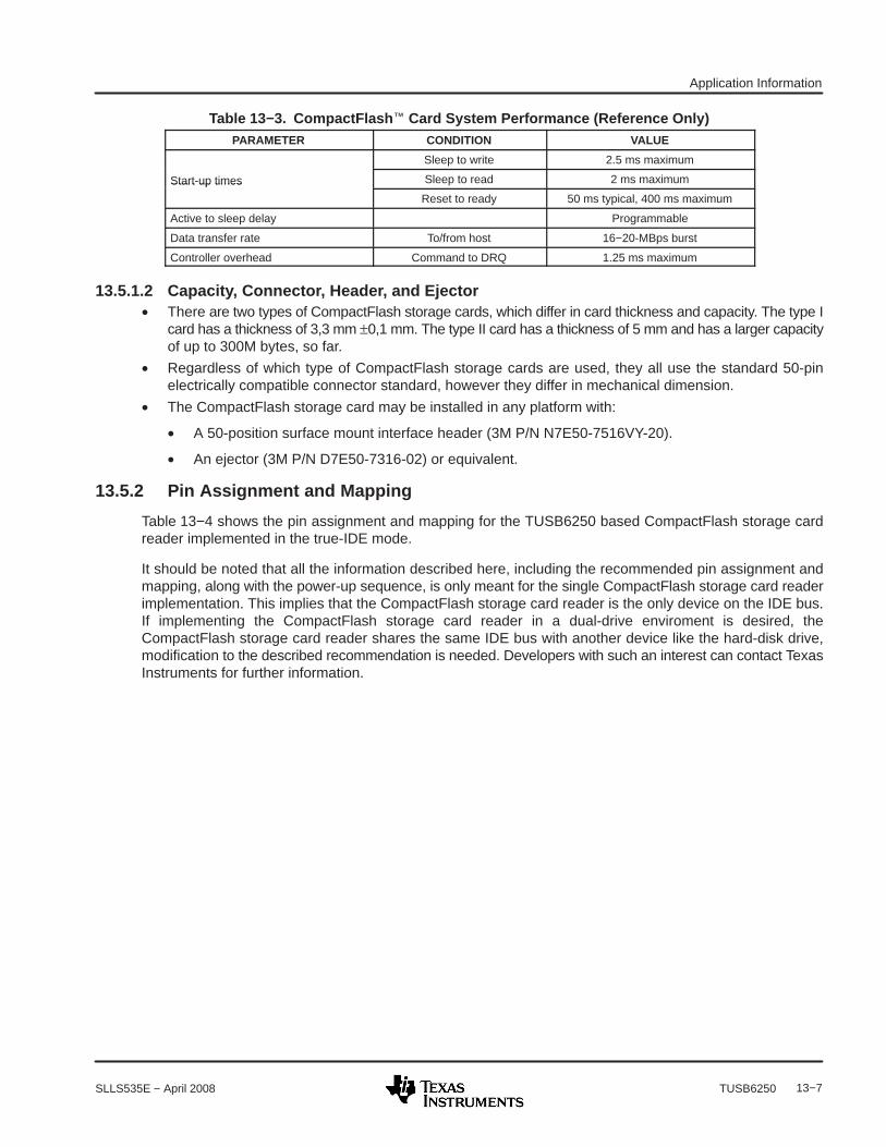
Application Information
13−7SLLS535E − April 2008 TUSB6250
Table 13−3. CompactFlash Card System Performance (Reference Only)PARAMETER CONDITION VALUE
Sleep to write 2.5 ms maximum
Start-up times Sleep to read 2 ms maximumStart-up times
Reset to ready 50 ms typical, 400 ms maximum
Active to sleep delay Programmable
Data transfer rate To/from host 16−20-MBps burst
Controller overhead Command to DRQ 1.25 ms maximum
13.5.1.2 Capacity, Connector, Header, and Ejector• There are two types of CompactFlash storage cards, which differ in card thickness and capacity. The type I
card has a thickness of 3,3 mm ±0,1 mm. The type II card has a thickness of 5 mm and has a larger capacityof up to 300M bytes, so far.
• Regardless of which type of CompactFlash storage cards are used, they all use the standard 50-pinelectrically compatible connector standard, however they differ in mechanical dimension.
• The CompactFlash storage card may be installed in any platform with:
• A 50-position surface mount interface header (3M P/N N7E50-7516VY-20).
• An ejector (3M P/N D7E50-7316-02) or equivalent.
13.5.2 Pin Assignment and Mapping
Table 13−4 shows the pin assignment and mapping for the TUSB6250 based CompactFlash storage cardreader implemented in the true-IDE mode.
It should be noted that all the information described here, including the recommended pin assignment andmapping, along with the power-up sequence, is only meant for the single CompactFlash storage card readerimplementation. This implies that the CompactFlash storage card reader is the only device on the IDE bus.If implementing the CompactFlash storage card reader in a dual-drive enviroment is desired, theCompactFlash storage card reader shares the same IDE bus with another device like the hard-disk drive,modification to the described recommendation is needed. Developers with such an interest can contact TexasInstruments for further information.
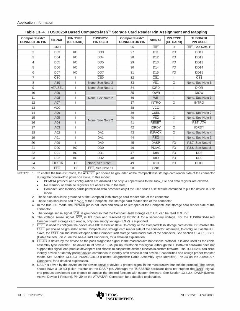
Application Information
13−8 SLLS535E − April 2008TUSB6250
Table 13−4. TUSB6250 Based CompactFlash Storage Card Reader Pin Assignment and MappingCompactFlash
CONNECTOR PINSIGNAL
PIN TYPE(CF CARD)
TUSB6250PIN USED
CompactFlash
CONNECTOR PINSIGNAL
PIN TYPE(CF CARD)
TUSB6250PIN USED
1 GND 26 CD1 O CD1, See Note 11
2 D03 I/O DD3 27 D11 I/O DD11
3 D04 I/O DD4 28 D12 I/O DD12
4 D05 I/O DD5 29 D13 I/O DD13
5 D06 I/O DD6 30 D14 I/O DD14
6 D07 I/O DD7 31 D15 I/O DD15
7 CS0 I CS0 32 CS1 I CS1
8 A10 I None, See Note 2 33 VS1 O None, See Note 5
9 ATA SEL I None, See Note 1 34 IORD I DIOR
10 A09 I 35 IOWR I DIOW
11 A08 I None, See Note 2 36 WE I None, See Note 3
12 A07 I
None, See Note 2
37 INTRQ O INTRQ
13 VCC 38 VCC
14 A06 I 39 CSEL I None, See Note 7
15 A05 INone, See Note 2
40 VS2 O None, See Note 6
16 A04 INone, See Note 2
41 RESET I RST_ATA
17 A03 I 42 IORDY O IORDY
18 A02 I DA2 43 INPACK O None, See Note 4
19 A01 I DA1 44 REG I None, See Note 3
20 A00 I DA0 45 DASP I/O P3.7, See Note 9
21 D00 I/O DD0 46 PDIAG I/O P3.6, See Note 8
22 D01 I/O DD1 47 D08 I/O DD8
23 D02 I/O DD2 48 D09 I/O DD9
24 IOCS16 O None, See Note10 49 D10 I/O DD10
25 CD2 O CD2, See Note 11 50 GND
NOTES: 1. To enable the true-IDE mode, the ATA SEL pin should be grounded at the CompactFlash storage card reader side of the connectorduring the power-off to power-on cycle. In this mode:• PCMCIA protocol and configuration are disabled and only I/O operations to the Task_File and data register are allowed.• No memory or attribute registers are accessible to the host.• CompactFlash memory cards permit 8-bit data accesses only if the user issues a set feature command to put the device in 8-bit
mode.2. These pins should be grounded at the CompactFlash storage card reader side of the connector.3. These pins should be tied to VCC at the CompactFlash storage card reader side of the connector.4. In the true-IDE mode, the INPACK pin is not used and should be left open at the CompactFlash storage card reader side of the
connector.5. The voltage sense signal, VS1, is grounded so that the CompactFlash storage card CIS can be read at 3.3 V.6. The voltage sense signal, VS2, is left open and reserved by PCMCIA for a secondary voltage. For the TUSB6250-based
CompactFlash storage card reader, only one supply voltage (3.3 V) is supported.7. CSEL is used to configure the device as a IDE master or slave. To configure the CompactFlash storage card as the IDE master, the
CSEL pin should be grounded at the CompactFlash storage card reader side of the connector; otherwise, to configure it as the IDEslave, the CSEL pin should be left open at the CompactFlash storage card reader side of the connector. See Section 13.4.2.1, CSEL(Cable Select), Pin 28 on the ATA/ATAPI Connector, for a detailed explanation.
8. PDIAG is driven by the device as the pass diagnostic signal in the master/slave handshake protocol. It is also used as the cableassembly type identifier. The device must have a 10-kΩ pullup resistor on this signal. Although the TUSB6250 hardware does notsupport this signal, end-product developers can choose to support the desired function in custom firmware. The TUSB6250 can issueidentify device or identify packet device commands to identify both device-0 and device-1 capabilities and assign proper transfermode. See Section 13.4.2.3, PDIAG:CBLID (Passed Diagnostics: Cable Assembly Type Identifier), Pin 34 on the ATA/ATAPIConnector, for a detailed explanation.
9. DASP is driven by the device as the device active or device-1 present signal in the master/slave handshake protocol. The deviceshould have a 10-kΩ pullup resistor on the DASP pin. Although the TUSB6250 hardware does not support the DASP signal,end-product developers can choose to support the desired function with custom firmware. See Section 13.4.2.4, DASP (DeviceActive, Device 1 Present), Pin 39 on the ATA/ATAPI Connector, for a detailed explanation.

Application Information
13−9SLLS535E − April 2008 TUSB6250
10. Because the CompactFlash storage card permits 8-bit data transfer only if a user issues a set feature command to put the devicein the 8-bit mode, there is no need to support it as long as the host driver prohibits such command. The IOCS16 pin at theCompactFlash storage card reader side of the connector should be left open. See Section 13.4.2.2, IOCS16, Pin 32 on theATA/ATAPI Connector, for a detailed explanation.
11. The CD1 and CD2 pins are card-detect pins that connect to ground on the CompactFlash storage card. They are used by the hostto determine that the CompactFlash storage card is fully inserted into its socket. A valid insertion is evaluated when both CD1 andCD2 are detected as GND by the host.
13.5.3 Power-Up Sequence
Because the CompactFlash storage card powers up into PC card ATA modes (not true-IDE modes), toconfigure the CompactFlash storage card into the true-IDE mode, the 50-pin CompactFlash socket must bepower cycled with the CompactFlash storage card inserted and the ATASEL pin asserted. This also must beaccomplished when removing and reinserting the CompactFlash storage card when the CompactFlashstorage card reader power is on.
To achieve this required power-up sequence, the recommended approaches for the end-product customfirmware to implement a CompactFlash storage card reader based on the TUSB6250 are described asfollows.
• The firmware can use the P2.0 pin as the power-up control signal to turn on/off the power to theCompactFlash storage card. To ensure enough drive strength, the developer should use active-low as thelogic level to turn on the reader.
• After a power-up reset to the TUSB6250, the firmware can toggle the P2.0 pin to turn on the power to theCompactFlash storage reader socket.
• Once CD1 and CD2 are both asserted (this means there is a CompactFlash storage card inserted), thefirmware must shut down the power to the CompactFlash storage card for a duration of about one second.Thereafter, the firmware must turn the power back on. This sequence ensures the ATASEL signal islatched during the power cycle, such that the true-IDE mode is enabled for the CompactFlash storagecard.

Application Information
13−10 SLLS535E − April 2008TUSB6250

MECHANICAL DATA
MTQF009A – OCTOBER 1994 – REVISED DECEMBER 1996
POST OFFICE BOX 655303 • DALLAS, TEXAS 75265
PFC (S-PQFP-G80) PLASTIC QUAD FLATPACK
4073177/B 11/96
40
210,13 NOM
0,25
0,750,45
Seating Plane
0,05 MIN
Gage Plane
0,27
41
0,17
20
60
1
61
80
SQ
SQ
12,20
13,8014,20
11,80
9,50 TYP
1,05
1,20 MAX
0,95
0,08
0,50 M0,08
0°–7°
NOTES: A. All linear dimensions are in millimeters.B. This drawing is subject to change without notice.C. Falls within JEDEC MS-026
IMPORTANT NOTICETexas Instruments Incorporated and its subsidiaries (TI) reserve the right to make corrections, modifications, enhancements, improvements,and other changes to its products and services at any time and to discontinue any product or service without notice. Customers shouldobtain the latest relevant information before placing orders and should verify that such information is current and complete. All products aresold subject to TI’s terms and conditions of sale supplied at the time of order acknowledgment.TI warrants performance of its hardware products to the specifications applicable at the time of sale in accordance with TI’s standardwarranty. Testing and other quality control techniques are used to the extent TI deems necessary to support this warranty. Except wheremandated by government requirements, testing of all parameters of each product is not necessarily performed.TI assumes no liability for applications assistance or customer product design. Customers are responsible for their products andapplications using TI components. To minimize the risks associated with customer products and applications, customers should provideadequate design and operating safeguards.TI does not warrant or represent that any license, either express or implied, is granted under any TI patent right, copyright, mask work right,or other TI intellectual property right relating to any combination, machine, or process in which TI products or services are used. Informationpublished by TI regarding third-party products or services does not constitute a license from TI to use such products or services or awarranty or endorsement thereof. Use of such information may require a license from a third party under the patents or other intellectualproperty of the third party, or a license from TI under the patents or other intellectual property of TI.Reproduction of TI information in TI data books or data sheets is permissible only if reproduction is without alteration and is accompaniedby all associated warranties, conditions, limitations, and notices. Reproduction of this information with alteration is an unfair and deceptivebusiness practice. TI is not responsible or liable for such altered documentation. Information of third parties may be subject to additionalrestrictions.Resale of TI products or services with statements different from or beyond the parameters stated by TI for that product or service voids allexpress and any implied warranties for the associated TI product or service and is an unfair and deceptive business practice. TI is notresponsible or liable for any such statements.TI products are not authorized for use in safety-critical applications (such as life support) where a failure of the TI product would reasonablybe expected to cause severe personal injury or death, unless officers of the parties have executed an agreement specifically governingsuch use. Buyers represent that they have all necessary expertise in the safety and regulatory ramifications of their applications, andacknowledge and agree that they are solely responsible for all legal, regulatory and safety-related requirements concerning their productsand any use of TI products in such safety-critical applications, notwithstanding any applications-related information or support that may beprovided by TI. Further, Buyers must fully indemnify TI and its representatives against any damages arising out of the use of TI products insuch safety-critical applications.TI products are neither designed nor intended for use in military/aerospace applications or environments unless the TI products arespecifically designated by TI as military-grade or "enhanced plastic." Only products designated by TI as military-grade meet militaryspecifications. Buyers acknowledge and agree that any such use of TI products which TI has not designated as military-grade is solely atthe Buyer's risk, and that they are solely responsible for compliance with all legal and regulatory requirements in connection with such use.TI products are neither designed nor intended for use in automotive applications or environments unless the specific TI products aredesignated by TI as compliant with ISO/TS 16949 requirements. Buyers acknowledge and agree that, if they use any non-designatedproducts in automotive applications, TI will not be responsible for any failure to meet such requirements.Following are URLs where you can obtain information on other Texas Instruments products and application solutions:Products ApplicationsAmplifiers amplifier.ti.com Audio www.ti.com/audioData Converters dataconverter.ti.com Automotive www.ti.com/automotiveDSP dsp.ti.com Broadband www.ti.com/broadbandClocks and Timers www.ti.com/clocks Digital Control www.ti.com/digitalcontrolInterface interface.ti.com Medical www.ti.com/medicalLogic logic.ti.com Military www.ti.com/militaryPower Mgmt power.ti.com Optical Networking www.ti.com/opticalnetworkMicrocontrollers microcontroller.ti.com Security www.ti.com/securityRFID www.ti-rfid.com Telephony www.ti.com/telephonyRF/IF and ZigBee® Solutions www.ti.com/lprf Video & Imaging www.ti.com/video
Wireless www.ti.com/wireless
Mailing Address: Texas Instruments, Post Office Box 655303, Dallas, Texas 75265Copyright © 2008, Texas Instruments Incorporated