tuning the exciton binding energies in single self-assembled
TRANSCRIPT

Tuning the Exciton Binding Energies in Single Self-Assembled InGaAs=GaAs Quantum Dotsby Piezoelectric-Induced Biaxial Stress
F. Ding,1,2,3,* R. Singh,3 J. D. Plumhof,1 T. Zander,3 V. Krapek,1 Y.H. Chen,2 M. Benyoucef,1 V. Zwiller,4 K. Dorr,5
G. Bester,3,† A. Rastelli,1,‡ and O.G. Schmidt1
1Institute for Integrative Nanosciences, IFW Dresden, Helmholtzstrasse 20, D-01069 Dresden, Germany2Key Laboratory of Semiconductor Materials Science, Institute of Semiconductors, Chinese Academy of Sciences,
Beijing 100083, China3Max-Planck-Institut fur Festkorperforschung, Heisenbergstrasse 1, D-70569 Stuttgart, Germany
4Kavli Institute of Nanoscience, Delft University of Technology, P.O. Box 5046, 2600 GA Delft, The Netherlands5Institute for Metallic Materials, IFW Dresden, Helmholtzstrasse 20, D-01069 Dresden, Germany
(Received 3 November 2009; published 12 February 2010)
We study the effect of an external biaxial stress on the light emission of single InGaAs=GaAsð001Þquantum dots placed onto piezoelectric actuators. With increasing compression, the emission blueshifts
and the binding energies of the positive trion (Xþ) and biexciton (XX) relative to the neutral exciton (X)
show a monotonic increase. This phenomenon is mainly ascribed to changes in electron and hole
localization and it provides a robust method to achieve color coincidence in the emission of X and
XX, which is a prerequisite for the possible generation of entangled photon pairs via the recently proposed
‘‘time reordering’’ scheme.
DOI: 10.1103/PhysRevLett.104.067405 PACS numbers: 78.67.Hc, 78.20.hb, 81.05.Ea, 81.40.Tv
Sources of entangled photon pairs on demand are amajor building block for quantum computation and com-munication [1]. Recently, the generation of entangled pho-ton pairs from semiconductor quantum dots (QDs) hasattracted great interest [2–5]. The polarization-entangledphotons are produced in an idealized QD with degenerateintermediate exciton states in the cascade: biexcitonðXXÞ ! excitonðXÞ ! ground state (G), where the polar-ization of a photon pair is determined by the spin of theintermediate exciton state [6]. However, real self-assembled QDs exhibit intermediate exciton ground statessplit into two states by an energy � called fine structuresplitting (FSS) [7]. This is the consequence of shape andatomistic crystal anisotropy and the electron-hole ex-change interactions [8]. The FSS in self-assembledInðGaÞAs=GaAs QDs grown along the [001] crystal direc-tion is typically quite large as compared to the radiativelinewidth (�1:0 �eV). The nonvanishing FSS encodes thewhich-path information and destroys the polarization en-tanglement. The generation of entangled photon pairs bysimple preselection of rare dots with � close to zero [2,4] orby spectral filtering [3] has been demonstrated.Furthermore, a number of postgrowth techniques havebeen used to reduce �, such as in-plane magnetic fields[9], lateral electric fields [10,11], uniaxial stress [12], andrapid thermal annealing [13].
An alternative proposal to generate entangled photonpairs from QDs, without any fundamental requirementson the FSS to be smaller than the radiative linewidth, isthe so-called time reordering scheme [14]. However, thisscheme requires the emission energies of X (EX) and XX(EXX) to be the same. In this scheme, one entangles the red
photons H1ðV2Þ and the blue photons V1ðH2Þ [see thecentral panel of Fig. 1(a)] across generations in a QD. It isaccomplished by performing a unitary operation (timereordering) U on the two-photon state such that
jh�HjUyHUV j�Vij> jh�Hj�Vij [14,15], where j�HðVÞi is
the wave packet resulting from the biexciton cascade emis-
FIG. 1 (color online). (a) Level schemes showing the XX-Xcascade. The solid (dashed) line represents the decay channelthat yields H (V) polarized photons. Across generation colorcoincidence of X and XX (EX ¼ EXX) can be achieved byapplying tensile (compressive) stress to a QD with positive(negative) EBðXXÞ. (b) Schematic drawing of the experimentand optical microscopy image of a 200 nm-thick GaAs mem-brane (inset). (c) Low temperature PL spectra of QDs withnegative (QD1) and positive (QD2) XX binding energy.
PRL 104, 067405 (2010) P HY S I CA L R EV I EW LE T T E R Sweek ending
12 FEBRUARY 2010
0031-9007=10=104(6)=067405(4) 067405-1 � 2010 The American Physical Society
sion. This novel concept is currently under vivid discussion[15–18]: On one hand the two-photon wave packet maysuffer significant dephasing after the time reordering, onthe other hand the emission energies EX and EXX in the as-grown QDs are usually different because of pronouncedinteractions between charge and spin carriers in a QD.
In this Letter we show that an external biaxial ten-sile (T) or compressive (C) stress can be used to achieveEX � EXX. Stress is provided in situ by placing a thinGaAs membrane containing self-assembled InGaAsQDs on top of a piezoelectric actuator, made of½PbðMg1=3Nb2=3ÞO3�0:72-½PbTiO3�0:28 (PMN-PT) [see
Fig. 1(b)]. With increasing compression, the relative spec-tral positions of different excitonic species (X, XX, andXþ) show subtle, but systematic changes: The bindingenergies EB of both Xþ and XX, defined as EBðXX=XþÞ ¼EX-EXX=Xþ increase in all studied QDs. Based upon
million-atom empirical pseudopotential many-body calcu-lations of realistic InGaAs=GaAs QDs, we ascribe thisphenomenon to the increase in electron-hole Coulombinteractions due to the increase in confinement of electronsand slight decrease in confinement of holes upon compres-sive biaxial stress. Finally, different from the behaviorobserved under in-plane uniaxial stress [12], biaxial straindoes not appreciably affect the FSS, a behavior which isalso expected from our calculations.
We fabricated 200 nm-thick GaAs membranes withembedded self-assembled InGaAs QDs, and then trans-ferred them onto a 300 �m-thick PMN-PT actuator viaPMMA resist [20]. A bias voltage V applied to the PMN-PT results in an out-of-plane electric field F which leads toan in-plane strain "k in the GaAs membrane and the QD
structure [see Fig. 1(b)]. The PMN-PT was poled so thatV > 0 (<0) corresponds to in-plane compressive (tensile)strain "k < 0 (>0). Figure 1(c) shows low-excitation
power photoluminescence (PL) spectra of two QDs withnegative EBðXXÞ (QD1) and positive EBðXXÞ (QD2). Theneutral exciton X and the biexciton XX are identified bypower- and polarization-dependent PL. (The latter allowsus also to determine the FSS of X and XX). An unpolarizedline lying at the higher energy side of X and XX is attrib-uted to positive trion Xþ emission. The assignment issupported by the background p-type doping of our struc-tures and by the correlation between EBðXþÞ and EBðXXÞobserved in all the studied dots [see Fig. 2(e)].
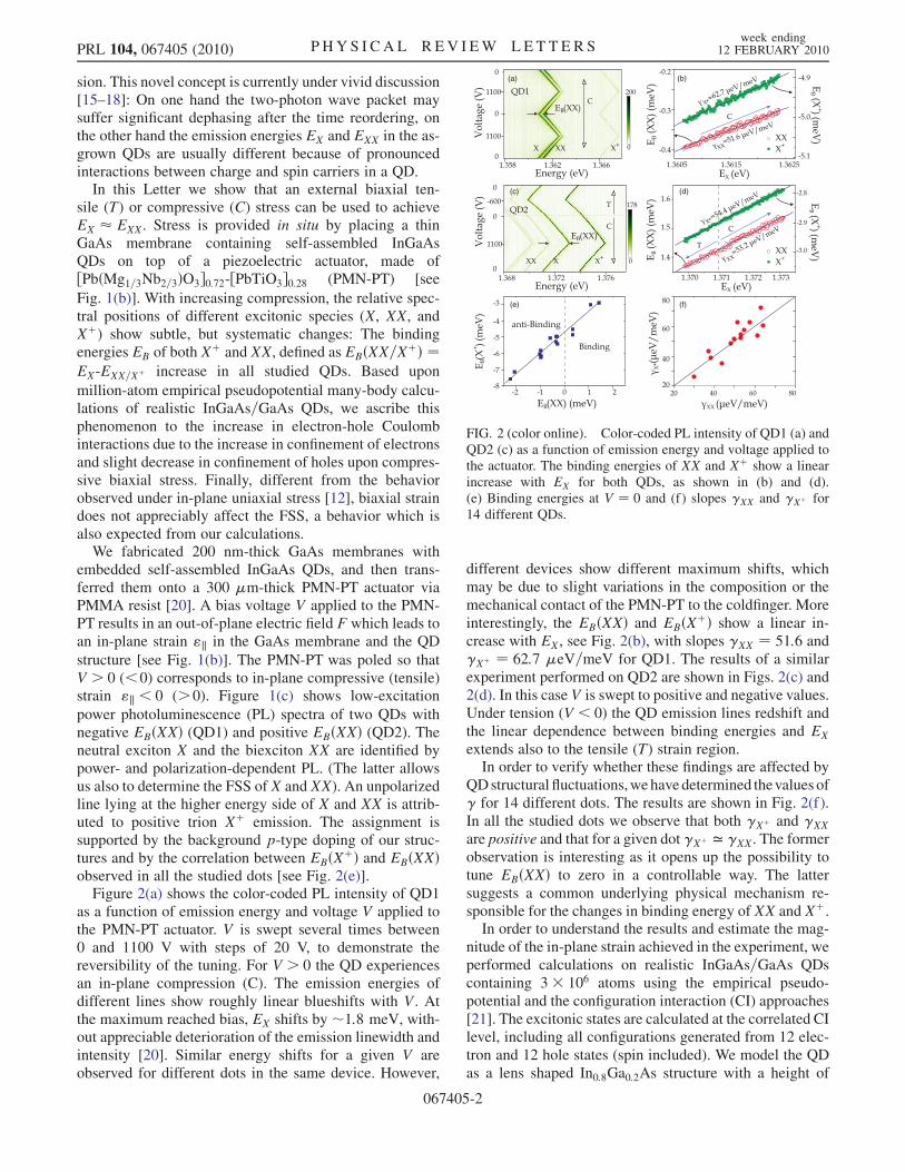
Figure 2(a) shows the color-coded PL intensity of QD1as a function of emission energy and voltage V applied tothe PMN-PT actuator. V is swept several times between0 and 1100 V with steps of 20 V, to demonstrate thereversibility of the tuning. For V > 0 the QD experiencesan in-plane compression (C). The emission energies ofdifferent lines show roughly linear blueshifts with V. Atthe maximum reached bias, EX shifts by �1:8 meV, with-out appreciable deterioration of the emission linewidth andintensity [20]. Similar energy shifts for a given V areobserved for different dots in the same device. However,
different devices show different maximum shifts, whichmay be due to slight variations in the composition or themechanical contact of the PMN-PT to the coldfinger. Moreinterestingly, the EBðXXÞ and EBðXþÞ show a linear in-crease with EX, see Fig. 2(b), with slopes �XX ¼ 51:6 and�Xþ ¼ 62:7 �eV=meV for QD1. The results of a similarexperiment performed on QD2 are shown in Figs. 2(c) and2(d). In this case V is swept to positive and negative values.Under tension (V < 0) the QD emission lines redshift andthe linear dependence between binding energies and EX
extends also to the tensile (T) strain region.In order to verify whether these findings are affected by
QDstructural fluctuations,wehavedetermined thevalues of� for 14 different dots. The results are shown in Fig. 2(f).In all the studied dots we observe that both �Xþ and �XX
are positive and that for a given dot �Xþ ’ �XX. The formerobservation is interesting as it opens up the possibility totune EBðXXÞ to zero in a controllable way. The lattersuggests a common underlying physical mechanism re-sponsible for the changes in binding energy of XX and Xþ.In order to understand the results and estimate the mag-
nitude of the in-plane strain achieved in the experiment, weperformed calculations on realistic InGaAs=GaAs QDscontaining 3� 106 atoms using the empirical pseudo-potential and the configuration interaction (CI) approaches[21]. The excitonic states are calculated at the correlated CIlevel, including all configurations generated from 12 elec-tron and 12 hole states (spin included). We model the QDas a lens shaped In0:8Ga0:2As structure with a height of
FIG. 2 (color online). Color-coded PL intensity of QD1 (a) andQD2 (c) as a function of emission energy and voltage applied tothe actuator. The binding energies of XX and Xþ show a linearincrease with EX for both QDs, as shown in (b) and (d).(e) Binding energies at V ¼ 0 and (f) slopes �XX and �Xþ for14 different QDs.
PRL 104, 067405 (2010) P HY S I CA L R EV I EW LE T T E R Sweek ending
12 FEBRUARY 2010
067405-2
2.5 nm and elliptical base of major (minor) axis of 10(7.5) nm along the ½1�10� ([110]) crystal direction.
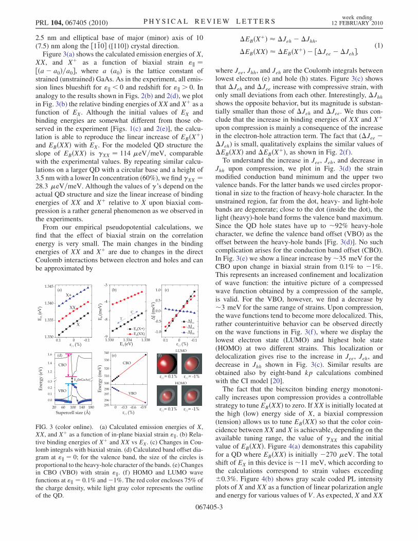
Figure 3(a) shows the calculated emission energies of X,XX, and Xþ as a function of biaxial strain "k ¼½ða� a0Þ=a0�, where a (a0) is the lattice constant ofstrained (unstrained) GaAs. As in the experiment, all emis-sion lines blueshift for "k < 0 and redshift for "k > 0. Inanalogy to the results shown in Figs. 2(b) and 2(d), we plotin Fig. 3(b) the relative binding energies of XX and Xþ as afunction of EX. Although the initial values of EX andbinding energies are somewhat different from those ob-served in the experiment [Figs. 1(c) and 2(e)], the calcu-lation is able to reproduce the linear increase of EBðXþÞand EBðXXÞ with EX. For the modeled QD structure theslope of EBðXXÞ is �XX ¼ 114 �eV=meV, comparablewith the experimental values. By repeating similar calcu-lations on a larger QD with a circular base and a height of3.5 nmwith a lower In concentration (60%), we find �XX ¼28:3 �eV=meV. Although the values of �’s depend on theactual QD structure and size the linear increase of bindingenergies of XX and Xþ relative to X upon biaxial com-pression is a rather general phenomenon as we observed inthe experiments.
From our empirical pseudopotential calculations, wefind that the effect of biaxial strain on the correlationenergy is very small. The main changes in the bindingenergies of XX and Xþ are due to changes in the directCoulomb interactions between electron and holes and canbe approximated by
�EBðXþÞ � �Jeh � �Jhh;
�EBðXXÞ � �EBðXþÞ � ½�Jee � �Jeh�;(1)
where Jee, Jhh, and Jeh are the Coulomb integrals betweenlowest electron (e) and hole (h) states. Figure 3(c) showsthat �Jeh and �Jee increase with compressive strain, withonly small deviations from each other. Interestingly, �Jhhshows the opposite behavior, but its magnitude is substan-tially smaller than those of �Jeh and �Jee. We thus con-clude that the increase in binding energies of XX and Xþupon compression is mainly a consequence of the increasein the electron-hole attraction term. The fact that (�Jee ��Jeh) is small, qualitatively explains the similar values of�EBðXXÞ and �EBðXþÞ, as shown in Fig. 2(f).To understand the increase in Jee, Jeh, and decrease in
Jhh upon compression, we plot in Fig. 3(d) the strainmodified conduction band minimum and the upper twovalence bands. For the latter bands we used circles propor-tional in size to the fraction of heavy-hole character. In theunstrained region, far from the dot, heavy- and light-holebands are degenerate; close to the dot (inside the dot), thelight (heavy)-hole band forms the valence band maximum.Since the QD hole states have up to �92% heavy-holecharacter, we define the valence band offset (VBO) as theoffset between the heavy-hole bands [Fig. 3(d)]. No suchcomplication arises for the conduction band offset (CBO).In Fig. 3(e) we show a linear increase by�35 meV for theCBO upon change in biaxial strain from 0.1% to �1%.This represents an increased confinement and localizationof wave function: the intuitive picture of a compressedwave function obtained by a compression of the sample,is valid. For the VBO, however, we find a decrease by�3 meV for the same range of strains. Upon compression,the wave functions tend to become more delocalized. This,rather counterintuitive behavior can be observed directlyon the wave functions in Fig. 3(f), where we display thelowest electron state (LUMO) and highest hole state(HOMO) at two different strains. This localization ordelocalization gives rise to the increase in Jee, Jeh, anddecrease in Jhh shown in Fig. 3(c). Similar results areobtained also by eight-band kp calculations combinedwith the CI model [20].The fact that the biexciton binding energy monotoni-
cally increases upon compression provides a controllablestrategy to tune EBðXXÞ to zero. If XX is initially located atthe high (low) energy side of X, a biaxial compression(tension) allows us to tune EBðXXÞ so that the color coin-cidence between XX and X is achievable, depending on theavailable tuning range, the value of �XX and the initialvalue of EBðXXÞ. Figure 4(a) demonstrates this capabilityfor a QD where EBðXXÞ is initially �270 �eV. The totalshift of EX in this device is �11 meV, which according tothe calculations correspond to strain values exceeding�0:3%. Figure 4(b) shows gray scale coded PL intensityplots of X and XX as a function of linear polarization angleand energy for various values of V. As expected, X and XX
FIG. 3 (color online). (a) Calculated emission energies of X,XX, and Xþ as a function of in-plane biaxial strain "k. (b) Rela-tive binding energies of Xþ and XX vs EX. (c) Changes in Cou-lomb integrals with biaxial strain. (d) Calculated band offset dia-gram at "k ¼ 0; for the valence band, the size of the circles is
proportional to the heavy-hole character of the bands. (e) Changesin CBO (VBO) with strain "k. (f) HOMO and LUMO wave
functions at "k ¼ 0:1% and�1%. The red color encloses 75% of
the charge density, while light gray color represents the outlineof the QD.
PRL 104, 067405 (2010) P HY S I CA L R EV I EW LE T T E R Sweek ending
12 FEBRUARY 2010
067405-3
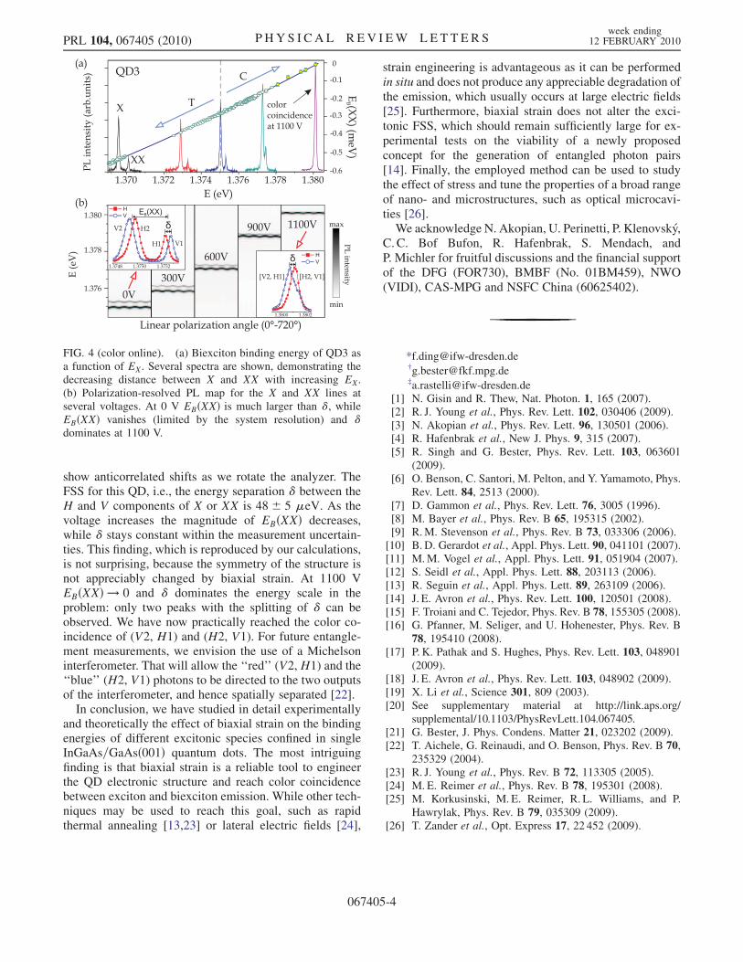
show anticorrelated shifts as we rotate the analyzer. TheFSS for this QD, i.e., the energy separation � between theH and V components of X or XX is 48� 5 �eV. As thevoltage increases the magnitude of EBðXXÞ decreases,while � stays constant within the measurement uncertain-ties. This finding, which is reproduced by our calculations,is not surprising, because the symmetry of the structure isnot appreciably changed by biaxial strain. At 1100 VEBðXXÞ ! 0 and � dominates the energy scale in theproblem: only two peaks with the splitting of � can beobserved. We have now practically reached the color co-incidence of (V2, H1) and (H2, V1). For future entangle-ment measurements, we envision the use of a Michelsoninterferometer. That will allow the ‘‘red’’ (V2, H1) and the‘‘blue’’ (H2, V1) photons to be directed to the two outputsof the interferometer, and hence spatially separated [22].
In conclusion, we have studied in detail experimentallyand theoretically the effect of biaxial strain on the bindingenergies of different excitonic species confined in singleInGaAs=GaAsð001Þ quantum dots. The most intriguingfinding is that biaxial strain is a reliable tool to engineerthe QD electronic structure and reach color coincidencebetween exciton and biexciton emission. While other tech-niques may be used to reach this goal, such as rapidthermal annealing [13,23] or lateral electric fields [24],
strain engineering is advantageous as it can be performedin situ and does not produce any appreciable degradation ofthe emission, which usually occurs at large electric fields[25]. Furthermore, biaxial strain does not alter the exci-tonic FSS, which should remain sufficiently large for ex-perimental tests on the viability of a newly proposedconcept for the generation of entangled photon pairs[14]. Finally, the employed method can be used to studythe effect of stress and tune the properties of a broad rangeof nano- and microstructures, such as optical microcavi-ties [26].We acknowledge N. Akopian, U. Perinetti, P. Klenovsky,
C. C. Bof Bufon, R. Hafenbrak, S. Mendach, andP. Michler for fruitful discussions and the financial supportof the DFG (FOR730), BMBF (No. 01BM459), NWO(VIDI), CAS-MPG and NSFC China (60625402).
*[email protected]†[email protected]‡[email protected]
[1] N. Gisin and R. Thew, Nat. Photon. 1, 165 (2007).[2] R. J. Young et al., Phys. Rev. Lett. 102, 030406 (2009).[3] N. Akopian et al., Phys. Rev. Lett. 96, 130501 (2006).[4] R. Hafenbrak et al., New J. Phys. 9, 315 (2007).[5] R. Singh and G. Bester, Phys. Rev. Lett. 103, 063601
(2009).[6] O. Benson, C. Santori, M. Pelton, and Y. Yamamoto, Phys.
Rev. Lett. 84, 2513 (2000).[7] D. Gammon et al., Phys. Rev. Lett. 76, 3005 (1996).[8] M. Bayer et al., Phys. Rev. B 65, 195315 (2002).[9] R.M. Stevenson et al., Phys. Rev. B 73, 033306 (2006).[10] B. D. Gerardot et al., Appl. Phys. Lett. 90, 041101 (2007).[11] M.M. Vogel et al., Appl. Phys. Lett. 91, 051904 (2007).[12] S. Seidl et al., Appl. Phys. Lett. 88, 203113 (2006).[13] R. Seguin et al., Appl. Phys. Lett. 89, 263109 (2006).[14] J. E. Avron et al., Phys. Rev. Lett. 100, 120501 (2008).[15] F. Troiani and C. Tejedor, Phys. Rev. B 78, 155305 (2008).[16] G. Pfanner, M. Seliger, and U. Hohenester, Phys. Rev. B
78, 195410 (2008).[17] P. K. Pathak and S. Hughes, Phys. Rev. Lett. 103, 048901
(2009).[18] J. E. Avron et al., Phys. Rev. Lett. 103, 048902 (2009).[19] X. Li et al., Science 301, 809 (2003).[20] See supplementary material at http://link.aps.org/
supplemental/10.1103/PhysRevLett.104.067405.[21] G. Bester, J. Phys. Condens. Matter 21, 023202 (2009).[22] T. Aichele, G. Reinaudi, and O. Benson, Phys. Rev. B 70,
235329 (2004).[23] R. J. Young et al., Phys. Rev. B 72, 113305 (2005).[24] M. E. Reimer et al., Phys. Rev. B 78, 195301 (2008).[25] M. Korkusinski, M. E. Reimer, R. L. Williams, and P.
Hawrylak, Phys. Rev. B 79, 035309 (2009).[26] T. Zander et al., Opt. Express 17, 22 452 (2009).
FIG. 4 (color online). (a) Biexciton binding energy of QD3 asa function of EX. Several spectra are shown, demonstrating thedecreasing distance between X and XX with increasing EX.(b) Polarization-resolved PL map for the X and XX lines atseveral voltages. At 0 V EBðXXÞ is much larger than �, whileEBðXXÞ vanishes (limited by the system resolution) and �dominates at 1100 V.
PRL 104, 067405 (2010) P HY S I CA L R EV I EW LE T T E R Sweek ending
12 FEBRUARY 2010
067405-4