ts_125102v071200p
DESCRIPTION
ts_125102v071200TRANSCRIPT
ETSI TS 125 102 V7.12.0 (2008-10)
Technical Specification
Universal Mobile Telecommunications System (UMTS);User Equipment (UE) radio transmission and reception (TDD)
(3GPP TS 25.102 version 7.12.0 Release 7)
ETSI
ETSI TS 125 102 V7.12.0 (2008-10) 1 3GPP TS 25.102 version 7.12.0 Release 7
Reference RTS/TSGR-0425102v7c0
Keywords UMTS
ETSI
650 Route des Lucioles F-06921 Sophia Antipolis Cedex - FRANCE
Tel.: +33 4 92 94 42 00 Fax: +33 4 93 65 47 16
Siret N° 348 623 562 00017 - NAF 742 C
Association à but non lucratif enregistrée à la Sous-Préfecture de Grasse (06) N° 7803/88
Important notice
Individual copies of the present document can be downloaded from: http://www.etsi.org
The present document may be made available in more than one electronic version or in print. In any case of existing or perceived difference in contents between such versions, the reference version is the Portable Document Format (PDF).
In case of dispute, the reference shall be the printing on ETSI printers of the PDF version kept on a specific network drive within ETSI Secretariat.
Users of the present document should be aware that the document may be subject to revision or change of status. Information on the current status of this and other ETSI documents is available at
http://portal.etsi.org/tb/status/status.asp
If you find errors in the present document, please send your comment to one of the following services: http://portal.etsi.org/chaircor/ETSI_support.asp
Copyright Notification
No part may be reproduced except as authorized by written permission. The copyright and the foregoing restriction extend to reproduction in all media.
© European Telecommunications Standards Institute 2008.
All rights reserved.
DECTTM, PLUGTESTSTM, UMTSTM, TIPHONTM, the TIPHON logo and the ETSI logo are Trade Marks of ETSI registered for the benefit of its Members.
3GPPTM is a Trade Mark of ETSI registered for the benefit of its Members and of the 3GPP Organizational Partners.
ETSI
ETSI TS 125 102 V7.12.0 (2008-10) 2 3GPP TS 25.102 version 7.12.0 Release 7
Intellectual Property Rights IPRs essential or potentially essential to the present document may have been declared to ETSI. The information pertaining to these essential IPRs, if any, is publicly available for ETSI members and non-members, and can be found in ETSI SR 000 314: "Intellectual Property Rights (IPRs); Essential, or potentially Essential, IPRs notified to ETSI in respect of ETSI standards", which is available from the ETSI Secretariat. Latest updates are available on the ETSI Web server (http://webapp.etsi.org/IPR/home.asp).
Pursuant to the ETSI IPR Policy, no investigation, including IPR searches, has been carried out by ETSI. No guarantee can be given as to the existence of other IPRs not referenced in ETSI SR 000 314 (or the updates on the ETSI Web server) which are, or may be, or may become, essential to the present document.
Foreword This Technical Specification (TS) has been produced by ETSI 3rd Generation Partnership Project (3GPP).
The present document may refer to technical specifications or reports using their 3GPP identities, UMTS identities or GSM identities. These should be interpreted as being references to the corresponding ETSI deliverables.
The cross reference between GSM, UMTS, 3GPP and ETSI identities can be found under http://webapp.etsi.org/key/queryform.asp.

ETSI
ETSI TS 125 102 V7.12.0 (2008-10) 3 3GPP TS 25.102 version 7.12.0 Release 7
Contents
Intellectual Property Rights ................................................................................................................................2
Foreword.............................................................................................................................................................2
Foreword...........................................................................................................................................................10
1 Scope ......................................................................................................................................................11
2 References ..............................................................................................................................................11
3 Definitions, symbols and abbreviations .................................................................................................11 3.1 Definitions........................................................................................................................................................11 3.2 (void) ................................................................................................................................................................12 3.3 Abbreviations ...................................................................................................................................................12
4 General ...................................................................................................................................................13 4.1 Relationship between Minimum Requirements and Test Requirements ..........................................................13 4.2 Power Classes...................................................................................................................................................13 4.3 Control and monitoring functions ....................................................................................................................13 4.3.1 Minimum requirement ................................................................................................................................13 4.4 RF requirements in later releases .....................................................................................................................14
5 Frequency bands and channel arrangement............................................................................................14 5.1 General .............................................................................................................................................................14 5.2 Frequency bands...............................................................................................................................................14 5.3 TX-RX frequency separation ...........................................................................................................................14 5.3.1 3.84 Mcps TDD Option ..............................................................................................................................14 5.3.2 1.28 Mcps TDD Option ..............................................................................................................................14 5.3.3 7.68 Mcps TDD Option ..............................................................................................................................15 5.4 Channel arrangement........................................................................................................................................15 5.4.1 Channel spacing..........................................................................................................................................15 5.4.1.1 3.84 Mcps TDD Option.........................................................................................................................15 5.4.1.2 1.28 Mcps TDD Option.........................................................................................................................15 5.4.1.3 7.68 Mcps TDD Option.........................................................................................................................15 5.4.2 Channel raster .............................................................................................................................................15 5.4.2.1 3.84 Mcps TDD Option.........................................................................................................................15 5.4.3 Channel number..........................................................................................................................................15 5.4.4 UARFCN ....................................................................................................................................................16 5.4.4.1 3.84 Mcps TDD Option.........................................................................................................................16 5.4.4.2 1.28 Mcps TDD Option.........................................................................................................................16 5.4.4.3 7.68 Mcps TDD Option.........................................................................................................................16
6 Transmitter characteristics .....................................................................................................................17 6.1 General .............................................................................................................................................................17 6.2 Transmit power ................................................................................................................................................17 6.2.1 User Equipment maximum output power ...................................................................................................17 6.2.1.1 3.84 Mcps TDD option .........................................................................................................................17 6.2.1.2 1.28 Mcps TDD option .........................................................................................................................17 6.2.1.3 7.68 Mcps TDD option .........................................................................................................................18 6.3 UE frequency stability......................................................................................................................................18 6.4 Output power dynamics....................................................................................................................................18 6.4.1 Power control..............................................................................................................................................18 6.4.1.1 3.84 Mcps option...................................................................................................................................18 6.4.1.1.1 Initial Accuracy ...............................................................................................................................18 6.4.1.1.2 Differential accuracy, controlled input ............................................................................................19 6.4.1.1.3 Differential accuracy, measured input .............................................................................................19 6.4.1.2 1.28 Mcps TDD Option.........................................................................................................................19 6.4.1.2.1 Open loop power control .................................................................................................................19 6.4.1.2.2 Closed loop power control...............................................................................................................19 6.4.1.2.2.1 Power control steps ....................................................................................................................19

ETSI
ETSI TS 125 102 V7.12.0 (2008-10) 4 3GPP TS 25.102 version 7.12.0 Release 7
6.4.1.2.2.1.1 Minimum requirement ...............................................................................................................20 6.4.1.3 7.68 Mcps option...................................................................................................................................20 6.4.1.3.1 Initial Accuracy ...............................................................................................................................20 6.4.1.3.2 Differential accuracy, controlled input ............................................................................................20 6.4.1.3.3 Differential accuracy, measured input .............................................................................................21 6.4.2 Minimum output power ..............................................................................................................................21 6.4.2.1 Minimum requirement ..........................................................................................................................21 6.4.2.1.1 3.84 Mcps TDD Option...................................................................................................................21 6.4.2.1.2 1.28 Mcps TDD Option...................................................................................................................21 6.4.2.1.3 7.68 Mcps TDD Option...................................................................................................................21 6.4.3 Out-of-synchronisation handling of output power......................................................................................21 6.4.3.1 Requirement for continuous transmission.............................................................................................22 6.4.3.1.1 3.84 Mcps TDD Option...................................................................................................................22 6.4.3.1.1.1 Minimum requirement ...............................................................................................................22 6.4.3.1.1.2 Test case.....................................................................................................................................22 6.4.3.1.2 1.28 Mcps TDD Option...................................................................................................................23 6.4.3.1.2.1 Minimum Requirement..............................................................................................................23 6.4.3.1.2.2 Test case.....................................................................................................................................23 6.4.3.1.3 7.68 Mcps TDD Option...................................................................................................................25 6.4.3.1.3.1 Minimum requirement ...............................................................................................................25 6.4.3.1.3.2 Test case.....................................................................................................................................25 6.4.3.2 Requirement for discontinuous transmission ........................................................................................26 6.4.3.2.1 3.84 Mcps TDD Option...................................................................................................................26 6.4.3.2.1.1 Minimum Requirement..............................................................................................................26 6.4.3.2.1.2 Test case.....................................................................................................................................26 6.4.3.2.2 1.28 Mcps TDD Option...................................................................................................................28 6.4.3.2.2.1 Minimum Requirement..............................................................................................................28 6.4.3.2.2.2 Test case.....................................................................................................................................29 6.4.3.2.3 7.68 Mcps TDD Option...................................................................................................................30 6.4.3.2.3.1 Minimum Requirement..............................................................................................................30 6.4.3.2.3.2 Test case.....................................................................................................................................30 6.5 Transmit ON/OFF power .................................................................................................................................32 6.5.1 Transmit OFF power...................................................................................................................................32 6.5.1.1 Minimum Requirement...............................................................................................................................32 6.5.2 Transmit ON/OFF Time mask ....................................................................................................................32 6.5.2.1 Minimum Requirement .........................................................................................................................33 6.5.2.1.1 3.84 Mcps TDD Option...................................................................................................................33 6.5.2.1.2 1.28 Mcps TDD Option...................................................................................................................33 6.5.2.1.3 7.68 Mcps TDD Option...................................................................................................................33 6.6 Output RF spectrum emissions.........................................................................................................................34 6.6.1 Occupied bandwidth ...................................................................................................................................34 6.6.1.1 3.84 Mcps TDD Option.........................................................................................................................34 6.6.1.2 1.28 Mcps TDD Option.........................................................................................................................34 6.6.1.3 7.68 Mcps TDD Option.........................................................................................................................34 6.6.2 Out of band emission ..................................................................................................................................34 6.6.2.1 Spectrum emission mask.......................................................................................................................34 6.6.2.1.1 3.84 Mcps TDD Option...................................................................................................................34 6.6.2.1.1.1 Minimum Requirement..............................................................................................................35 6.6.2.1.2 1.28 Mcps TDD Option...................................................................................................................35 6.6.2.1.2.1 Minimum Requirement..............................................................................................................35 6.6.2.1.3 7.68 Mcps TDD Option...................................................................................................................36 6.6.2.1.3.1 Minimum Requirement..............................................................................................................36 6.6.2.2 Adjacent Channel Leakage power Ratio (ACLR).................................................................................37 6.6.2.2.1 Minimum requirement.....................................................................................................................37 6.6.2.2.1.1 3.84 Mcps TDD Option .............................................................................................................37 6.6.2.2.1.2 1.28 Mcps TDD Option .............................................................................................................38 6.6.2.2.1.3 7.68 Mcps TDD Option .............................................................................................................38 6.6.3 Spurious emissions .....................................................................................................................................38 6.6.3.1 Minimum Requirement .........................................................................................................................38 6.6.3.1.1 3.84 Mcps TDD Option...................................................................................................................38 6.6.3.1.2 1.28 Mcps TDD Option...................................................................................................................39 6.6.3.1.3 7.68 Mcps TDD Option...................................................................................................................39
ETSI
ETSI TS 125 102 V7.12.0 (2008-10) 5 3GPP TS 25.102 version 7.12.0 Release 7
6.7 Transmit intermodulation .................................................................................................................................40 6.7.1 Minimum requirement ................................................................................................................................40 6.7.1.1 3.84 Mcps TDD Option.........................................................................................................................40 6.7.1.2 1.28 Mcps TDD Option.........................................................................................................................40 6.7.1.3 7.68 Mcps TDD Option.........................................................................................................................41 6.8 Transmit Modulation........................................................................................................................................41 6.8.1 Transmit pulse shape filter..........................................................................................................................41 6.8.2 Error Vector Magnitude..............................................................................................................................41 6.8.2.1 Minimum Requirement .........................................................................................................................41 6.8.3 Peak Code Domain Error ............................................................................................................................41 6.8.3.1 Minimum Requirement .........................................................................................................................42
7 Receiver characteristics..........................................................................................................................42 7.1 General .............................................................................................................................................................42 7.2 Diversity characteristics ...................................................................................................................................42 7.3 Reference sensitivity level................................................................................................................................42 7.3.1 Minimum Requirements .............................................................................................................................43 7.3.1.1 3.84 Mcps TDD Option.........................................................................................................................43 7.3.1.2 1.28 Mcps TDD Option.........................................................................................................................43 7.3.1.3 7.68 Mcps TDD Option.........................................................................................................................43 7.4 Maximum input level .......................................................................................................................................43 7.4.1 Minimum Requirements for DPCH reception ............................................................................................43 7.4.1.1 3.84 Mcps TDD Option.........................................................................................................................43 7.4.1.2 1.28 Mcps TDD Option.........................................................................................................................44 7.4.1.3 7.68 Mcps TDD Option.........................................................................................................................44 7.4.2 Minimum Requirements for HS-PDSCH reception....................................................................................44 7.4.2.1 3.84 Mcps TDD Option.........................................................................................................................44 7.4.2.2 1.28 Mcps TDD Option.........................................................................................................................44 7.5 Adjacent Channel Selectivity (ACS)................................................................................................................45 7.5.1 Minimum Requirement...............................................................................................................................45 7.5.1.1 3.84 Mcps TDD Option.........................................................................................................................45 7.5.1.2 1.28 Mcps TDD Option.........................................................................................................................45 7.5.1.3 7.68 Mcps TDD Option.........................................................................................................................46 7.6 Blocking characteristics ...................................................................................................................................46 7.6.1 Minimum Requirement...............................................................................................................................46 7.6.1.1 3.84 Mcps TDD Option.........................................................................................................................46 7.6.1.2 1.28 Mcps TDD Option.........................................................................................................................48 7.6.1.3 7.68 Mcps TDD Option.........................................................................................................................48 7.7 Spurious response.............................................................................................................................................50 7.7.1 Minimum Requirement...............................................................................................................................50 7.7.1.1 3.84 Mcps TDD Option.........................................................................................................................50 7.7.1.2 1.28 Mcps TDD Option.........................................................................................................................50 7.7.1.3 7.68 Mcps TDD Option.........................................................................................................................50 7.8 Intermodulation characteristics ........................................................................................................................51 7.8.1 Minimum Requirements .............................................................................................................................51 7.8.1.1 3.84 Mcps TDD Option.........................................................................................................................51 7.8.1.2 1.28 Mcps TDD Option.........................................................................................................................51 7.8.1.3 7.68 Mcps TDD Option.........................................................................................................................51 7.9 Spurious emissions ...........................................................................................................................................52 7.9.1 Minimum Requirement...............................................................................................................................52 7.9.1.1 3.84 Mcps TDD Option.........................................................................................................................52 7.9.1.2 1.28 Mcps TDD Option.........................................................................................................................52 7.9.1.3 7.68 Mcps TDD Option.........................................................................................................................53
8 Performance requirement .......................................................................................................................53 8.1 General .............................................................................................................................................................53 8.2 Demodulation in static propagation conditions ................................................................................................53 8.2.1 Demodulation of DCH................................................................................................................................53 8.2.1.1 Minimum requirement ..........................................................................................................................54 8.2.1.1.1 3.84 Mcps TDD Option...................................................................................................................54 8.2.1.1.2 1.28 Mcps TDD Option...................................................................................................................54 8.2.1.1.3 7.68 Mcps TDD Option...................................................................................................................55
ETSI
ETSI TS 125 102 V7.12.0 (2008-10) 6 3GPP TS 25.102 version 7.12.0 Release 7
8.3 Demodulation of DCH in multipath fading conditions ....................................................................................55 8.3.1 Multipath fading Case 1..............................................................................................................................55 8.3.1.1 Minimum requirement ..........................................................................................................................55 8.3.1.1.1 3.84 Mcps TDD Option...................................................................................................................55 8.3.1.1.2 1.28 Mcps TDD Option...................................................................................................................56 8.3.1.1.3 7.68 Mcps TDD Option...................................................................................................................57 8.3.2 Multipath fading Case 2..............................................................................................................................57 8.3.2.1 Minimum requirement ..........................................................................................................................57 8.3.2.1.1 3.84 Mcps TDD Option...................................................................................................................57 8.3.2.1.2 1.28 Mcps TDD Option...................................................................................................................58 8.3.2.1.3 7.68 Mcps TDD Option...................................................................................................................59 8.3.3 Multipath fading Case 3..............................................................................................................................59 8.3.3.1 Minimum requirement ..........................................................................................................................60 8.3.3.1.1 3.84 Mcps TDD Option...................................................................................................................60 8.3.3.1.2 1.28 Mcps TDD Option...................................................................................................................61 8.3.3.1.3 7.68 Mcps TDD Option...................................................................................................................61 8.4 Base station transmit diversity mode for 3.84 Mcps TDD Option ...................................................................62 8.4.1 Demodulation of BCH in SCTD mode.......................................................................................................62 8.4.1.1 Minimum requirement ..........................................................................................................................62 8.5 Power control in downlink ...............................................................................................................................62 8.5.1 Power control in downlink, constant BLER target .....................................................................................62 8.5.1.1 Minimum requirements 3.84 Mcps TDD option...................................................................................62 8.5.1.2 Minimum requirements 1.28 Mcps TDD option...................................................................................63 8.6 Uplink Power Control for 3.84 Mcps TDD Option..........................................................................................64 8.6.1 Test Conditions ...........................................................................................................................................64 8.6.2 Performance................................................................................................................................................64
9 Performance requirements (HSDPA) .....................................................................................................65 9.1 Performance requirement for 3.84 Mcps TDD option......................................................................................65 9.1.1 HS-DSCH throughput for fixed reference channels ...................................................................................65 9.1.1.1 Minimum requirement QPSK, Fixed Reference Channel, 7,3 Mbps - Category 8 - UE.......................65 9.1.1.2 Minimum requirement 16QAM, Fixed Reference Channel, 7,3 Mbps - Category 8 - UE....................66 9.1.2 HS-DSCH throughput for Variable Reference Channels............................................................................67 9.1.2.1 Minimum requirement Variable Reference Channel, 7,3 Mbps - Category 8 - UE ..............................67 9.1.3 Reporting of Channel Quality Indicator................................................................................................68 9.1.3.1 Minimum requirement Channel Quality Indicator, 7,3 Mbps - Category 8 - UE..................................68 9.1.4 HS-SCCH Detection Performance ...................................................................................................................69 9.1.4.1 Minimum Requirements for HS-SCCH Detection .....................................................................................69 9.2 Performance requirements for 1.28 Mcps TDD option ....................................................................................70 9.2.1 HS-DSCH throughput for fixed reference channels ...................................................................................70 9.2.1.1 Category 1, 0.5Mbps UE class ..............................................................................................................70 9.2.1.2 Category 4, 1.1Mbps UE class ..............................................................................................................71 9.2.1.3 Category 7, 1.6Mbps UE class ..............................................................................................................72 9.2.1.4 Category 10, 2.2Mbps UE class ............................................................................................................73 9.2.1.5 Category 13, 2.8Mbps UE class ............................................................................................................73 9.2.2 HS-DSCH throughput for Variable Reference Channels............................................................................74 9.2.2.1 Category 1, 0.5Mbps UE class ..............................................................................................................74 9.2.2.2 Category 4, 1.1Mbps UE class ..............................................................................................................75 9.2.2.3 Category 7, 1.6Mbps UE class ..............................................................................................................76 9.2.2.4 Category 10, 2.2 Mbps UE class ...........................................................................................................77 9.2.2.5 Category 13, 2.8 Mbps UE class ...........................................................................................................78 9.2.3 Reporting of Channel Quality Indicator ...........................................................................................................79 9.2.3.1 Minimum Requirement, Channel Quality Indicator - 1.4Mbps UE class .............................................79 9.2.4 HS-SCCH Detection Performance ...................................................................................................................80 9.2.4.1 Minimum Requirements for HS-SCCH Detection .....................................................................................80 9.2.5 PLCCH Detection Performance .......................................................................................................................81 9.2.4.1 Minimum Requirements .............................................................................................................................81 9.3 Performance requirement for 7.68 Mcps TDD option......................................................................................82 9.3.1 HS-DSCH throughput for fixed reference channels ...................................................................................82 9.3.1.1 Minimum requirement QPSK, Fixed Reference Channel, 5,3 Mbps - Category 8 - UE.......................82 9.3.1.2 Minimum requirement 16 QAM, Fixed Reference Channel, 5,3 Mbps - Category 8 - UE...................83 9.3.2 (void) ................................................................................................................................................................84

ETSI
ETSI TS 125 102 V7.12.0 (2008-10) 7 3GPP TS 25.102 version 7.12.0 Release 7
9.3.3 (void) ................................................................................................................................................................84 9.3.4 HS-SCCH Detection Performance ...................................................................................................................84 9.3.4.1 Minimum Requirements for HS-SCCH Detection .....................................................................................84
10 Performance requirements (MBMS) ......................................................................................................85 10.1 Demodulation of MCCH ..................................................................................................................................85 10.1.1 Minimum requirement ................................................................................................................................85 10.1.1.1 3.84 Mcps TDD Option.........................................................................................................................85 10.1.1.2 1.28 Mcps TDD Option.........................................................................................................................86 10.1.1.3 7.68 Mcps TDD Option.........................................................................................................................86 10.1.2 MBSFN capable UE ...................................................................................................................................86 10.1.2.1 3.84 Mcps TDD Option.........................................................................................................................87 10.1.2.2 1.28 Mcps TDD Option.........................................................................................................................87 10.1.2.3 7.68 Mcps TDD Option.........................................................................................................................88 10.2 Demodulation of MTCH ..................................................................................................................................88 10.2.1 Minimum requirement ................................................................................................................................88 10.2.1.1 3.84 Mcps TDD Option.........................................................................................................................88 10.2.1.2 1.28 Mcps TDD Option.........................................................................................................................89 10.2.1.3 7.68 Mcps TDD Option.........................................................................................................................89 10.2.2 MBSFN capable UE ...................................................................................................................................90 10.2.2.1 3.84 Mcps TDD Option.........................................................................................................................90 10.2.2.2 1.28 Mcps TDD Option.........................................................................................................................90 10.2.2.3 7.68 Mcps TDD Option.........................................................................................................................91 10.2.3 MBSFN TDD & FDD same platform sharing ............................................................................................92 10.2.3.1 3.84 Mcps TDD Option.........................................................................................................................92 10.2.3.2 (void).....................................................................................................................................................92 10.2.3.3 7.68 Mcps TDD Option.........................................................................................................................92 10.3 Demodulation of MTCH and cell identification...............................................................................................93 10.3.1 Minimum requirement ................................................................................................................................93 10.3.1.1 (void).....................................................................................................................................................93 10.3.1.2 1.28 Mcps TDD Option.........................................................................................................................93
11 Performance requirement (E-DCH) .......................................................................................................94 11.1 Detection of E-DCH HARQ ACK Indicator Channel (E-HICH).....................................................................94 11.1.1 Minimum requirement ................................................................................................................................94 11.1.1.1 3.84 Mcps TDD Option.........................................................................................................................94 11.1.1.2 1.28 Mcps TDD Option.........................................................................................................................94 11.1.1.3 7.68 Mcps TDD Option.........................................................................................................................95 11.2 Demodulation of E-DCH Absolute Grant Channel (E-AGCH) .......................................................................95 11.2.1 Minimum requirement ................................................................................................................................95 11.2.1.1 3.84 Mcps TDD Option.........................................................................................................................95 11.2.1.2 1.28 Mcps TDD Option.........................................................................................................................96 11.2.1.3 7.68 Mcps TDD Option.........................................................................................................................96
Annex A (normative): Measurement channels ..................................................................................98
A.1 (void) ......................................................................................................................................................98
A.2 Reference measurement channel ............................................................................................................98 A.2.1 UL reference measurement channel (12.2 kbps) ..............................................................................................98 A.2.1.1 3.84 Mcps TDD Option ..............................................................................................................................98 A.2.1.2 1.28 Mcps TDD Option ..............................................................................................................................99 A.2.1.3 7.68 Mcps TDD Option ............................................................................................................................101 A.2.2 DL reference measurement channel (12.2 kbps) ............................................................................................102 A.2.2.1 3.84 Mcps TDD Option ............................................................................................................................102 A.2.2.2 1.28 Mcps TDD Option ............................................................................................................................103 A.2.2.3 7.68 Mcps TDD Option ............................................................................................................................104 A.2.3 DL reference measurement channel (64 kbps) ...............................................................................................105 A.2.3.1 3.84 Mcps TDD Option ............................................................................................................................105 A.2.3.2 1.28 Mcps TDD Option ............................................................................................................................106 A.2.3.3 7.68 Mcps TDD Option ............................................................................................................................107 A.2.4 DL reference measurement channel (144 kbps) .............................................................................................108 A.2.4.1 3.84 Mcps TDD Option ............................................................................................................................108
ETSI
ETSI TS 125 102 V7.12.0 (2008-10) 8 3GPP TS 25.102 version 7.12.0 Release 7
A.2.4.2 1.28 Mcps TDD Option ............................................................................................................................110 A.2.4.3 7.68 Mcps TDD Option ............................................................................................................................111 A.2.5 DL reference measurement channel (384 kbps) .............................................................................................113 A.2.5.1 3.84 Mcps TDD Option ............................................................................................................................113 A.2.5.2 1.28 Mcps TDD Option ............................................................................................................................115 A.2.5.3 7.68 Mcps TDD Option ............................................................................................................................116 A.2.6 BCH reference measurement channel ............................................................................................................117 A.2.6.1 3.84 Mcps TDD Option ............................................................................................................................117 A.2.6.2 1.28 Mcps TDD Option ............................................................................................................................118 A.2.6.3 7.68 Mcps TDD Option ............................................................................................................................118 A.2.7 UL multi code reference measurement channel (12.2 kbps) ..........................................................................119 A.2.7.1 3.84 Mcps TDD Option ............................................................................................................................119 A.2.7.2 1.28 Mcps TDD Option ............................................................................................................................120 A.2.7.3 7.68 Mcps TDD Option ............................................................................................................................121 A.2.8 DL reference measurement channel (2 Mbps)................................................................................................123 A.2.8.1 3.84 Mcps TDD Option ............................................................................................................................123 A.2.8.2 1.28 Mcps TDD Option ............................................................................................................................125 A.2.8.3 7.68 Mcps TDD Option ............................................................................................................................126 A.2.9 DL reference measurement channel (12.2 kbps) for MBSFN only UEs ........................................................128 A.2.9.1 3.84 Mcps TDD Option ............................................................................................................................128 A.2.9.2 VOID ........................................................................................................................................................129 A.2.9.3 7.68 Mcps TDD Option ............................................................................................................................129
A.3 HSDPA reference measurement channels............................................................................................130 A.3.1 HSDPA reference measurement channels for 3,84 Mcps TDD option ..........................................................130 A.3.1.1 Reference measurement channels for 7,3 Mbps - Category 8 - UE ..........................................................130 A.3.1.1.1 QPSK modulation scheme for test 1, 2, 3 ...........................................................................................130 A.3.1.1.2 QPSK modulation scheme for test 4 ...................................................................................................131 A.3.1.1.3 16QAM modulation scheme for test 1, 2, 3 ........................................................................................132 A.3.1.1.4 16QAM modulation scheme for test 4 ................................................................................................133 A.3.2 HSDPA reference measurement channels for 1.28 Mcps TDD option ..........................................................133 A.3.2.1 Reference measurement channels for 0.5 Mbps UE class ........................................................................133 A.3.2.1.1 QPSK modulation scheme ..................................................................................................................133 A.3.2.2 Reference measurement channels for 1.1 Mbps UE class ........................................................................134 A.3.2.2.1 QPSK modulation scheme ..................................................................................................................134 A.3.2.2.2 16QAM modulation scheme ...............................................................................................................134 A.3.2.3 Reference measurement channels for 1.6 Mbps UE class ........................................................................135 A.3.2.3.1 QPSK modulation scheme ..................................................................................................................135 A.3.2.3.2 16QAM modulation scheme ...............................................................................................................136 A.3.2.4 Reference measurement channels for 2.2 Mbps UE class ........................................................................137 A.3.2.4.1 QPSK modulation scheme ..................................................................................................................137 A.3.2.4.2 16QAM modulation scheme ...............................................................................................................138 A.3.2.5 Reference measurement channels for 2.8 Mbps UE class ........................................................................139 A.3.2.5.1 QPSK modulation scheme ..................................................................................................................139 A.3.2.5.2 16QAM modulation scheme ...............................................................................................................140 A.3.2.6 PLCCH reference measurement channel ..................................................................................................141 A.3.2.2 PLCCH reference measurement channel ..................................................................................................141 A.3.2A HSDPA reference measurement channels for 7,68 Mcps TDD option ..........................................................142 A.3.2A.1 Reference measurement channels for 5,3 Mbps - Category 8 - UE ..........................................................142 A.3.2A.1.1 QPSK modulation scheme for test 1, 2, 3 & 4 ....................................................................................142 A.3.2A.1.2 16QAM modulation scheme for test 1, 2, 3 & 4 .................................................................................143 A.3.3 Variable Reference Channel definition for 3,84 Mcps and 1,28 Mcps TDD options.....................................143
A.4 Downlink reference parameter for MBMS tests ..................................................................................144 A.4.1 MCCH ............................................................................................................................................................144 A.4.1.1 3.84 Mcps TDD Option ............................................................................................................................144 A.4.1.2 1.28 Mcps TDD Option ............................................................................................................................144 A.4.1.3 7.68 Mcps TDD Option ............................................................................................................................145 A.4.2 MTCH ............................................................................................................................................................146 A.4.2.1 3.84 Mcps TDD Option ............................................................................................................................146 A.4.2.2 1.28 Mcps TDD Option ............................................................................................................................146 A.4.2.3 7.68 Mcps TDD Option ............................................................................................................................147

ETSI
ETSI TS 125 102 V7.12.0 (2008-10) 9 3GPP TS 25.102 version 7.12.0 Release 7
Annex B (normative): Propagation conditions................................................................................149
B.1 Static propagation condition.................................................................................................................149
B.2 Multi-path fading propagation conditions............................................................................................149 B.2.1 3.84 Mcps TDD Option..................................................................................................................................149 B.2.2 1.28 Mcps TDD Option..................................................................................................................................151 B.2.3 7.68 Mcps TDD Option..................................................................................................................................153
Annex C (normative): Environmental conditions ...........................................................................156
C.1 General .................................................................................................................................................156
C.2 Environmental requirements for the UE ..............................................................................................156 C.2.1 Temperature ...................................................................................................................................................156 C.2.2 Voltage ...........................................................................................................................................................156 C.2.3 Vibration.........................................................................................................................................................157
Annex D (informative): Terminal capabilities (TDD) .......................................................................158
Annex E (informative): Change request history................................................................................159
History ............................................................................................................................................................162

ETSI
ETSI TS 125 102 V7.12.0 (2008-10) 103GPP TS 25.102 version 7.12.0 Release 7
Foreword This Technical Specification has been produced by the 3GPP.
The contents of the present document are subject to continuing work within the TSG and may change following formal TSG approval. Should the TSG modify the contents of this TS, it will be re-released by the TSG with an identifying change of release date and an increase in version number as follows:
Version 3.y.z
where:
x the first digit:
1 presented to TSG for information;
2 presented to TSG for approval;
3 Indicates TSG approved document under change control.
y the second digit is incremented for all changes of substance, i.e. technical enhancements, corrections, updates, etc.
z the third digit is incremented when editorial only changes have been incorporated in the specification;

ETSI
ETSI TS 125 102 V7.12.0 (2008-10) 113GPP TS 25.102 version 7.12.0 Release 7
1 Scope This document establishes the minimum RF characteristics of all three options of the TDD mode of UTRA. The three options are the 3.84 Mcps, 1.28 Mcps and 7.68 Mcps options respectively. The requirements are listed in different subsections only if the parameters deviate.
2 References The following documents contain provisions, which, through reference in this text, constitute provisions of the present document.
• References are either specific (identified by date of publication, edition number, version number, etc.) or non-specific.
• For a specific reference, subsequent revisions do not apply.
• For a non-specific reference, the latest version applies. In the case of a reference to a 3GPP document (including a GSM document), a non-specific reference implicitly refers to the latest version of that document in the same Release as the present document.
[1] ETSI ETR 273-1-2: "Electromagnetic compatibility and Radio spectrum Matters (ERM); Improvement of radiated methods of measurement (using test sites) and evaluation of the corresponding measurement uncertainties; Part 1: Uncertainties in the measurement of mobile radio equipment characteristics; Sub-part 2: Examples and annexes".
[2] 3GPP TS 25.306: "UE Radio Access capabilities definition".
[3] ITU-R Recommendation SM.329: "Unwanted emissions in the spurious domain".
[4] 3GPP TS 25.307: "Requirements on User Equipments (UEs) supporting a release-independent frequency band".
3 Definitions, symbols and abbreviations
3.1 Definitions For the purposes of the present document, the following definitions apply:
Power Spectral Density: The units of Power Spectral Density (PSD) are extensively used in this document. PSD is a function of power versus frequency and when integrated across a given bandwidth, the function represents the mean power in such a bandwidth. When the mean power is normalised to (divided by) the chip-rate it represents the mean energy per chip. Some signals are directly defined in terms of energy per chip, (DPCH_Ec, Ec, and P-CCPCH_Ec) and others defined in terms of PSD (Io, Ioc, Ior and Îor). There also exist quantities that are a ratio of energy per chip to PSD (DPCH_Ec/Ior, Ec/Ior etc.). This is the common practice of relating energy magnitudes in communication systems.
It can be seen that if both energy magnitudes in the ratio are divided by time, the ratio is converted from an energy ratio to a power ratio, which is more useful from a measurement point of view. It follows that an energy per chip of X dBm/3.84 MHz (3.84 Mcps TDD option) or X dBm/1.28 MHz (1.28 Mcps TDD option) can be expressed as a mean power per chip of X dBm. Similarly, a signal PSD of Y dBm/3.84 MHz (3.84 Mcps TDD option) or Y dBm/1.28 MHz (1.28 Mcps TDD option) can be expressed as a signal power of Y dBm.
Maximum Output Power: This is a measure of the maximum power the UE can transmit (i.e. the actual power as would be measured assuming no measurement error) in a bandwidth of at least (1+ α) times the chip rate of the radio access mode. The period of measurement shall be a transmit timeslot excluding the guard period.
ETSI
ETSI TS 125 102 V7.12.0 (2008-10) 123GPP TS 25.102 version 7.12.0 Release 7
Mean Power: When applied to a CDMA modulated signal this is the power (transmitted or received) in a bandwidth of at least (1+ α) times the chip rate of the radio access mode. The period of measurement shall be a transmit timeslot excluding the guard period unless otherwise stated.
RRC Filtered Mean Power: The mean power as measured through a root raised cosine filter with roll-off factor α and a bandwidth equal to the chip rate of the radio access mode.
Nominal Maximum Output Power: This is the nominal power defined by the UE power class. The period of measurement shall be a transmit timeslot excluding the guard period.
Received Signal Code Power (RSCP): Given only signal power is received, the RRC filtered mean power of the received signal after despreading and combining.
Interference Signal Code Power (ISCP): Given only interference power is received, the RRC filtered mean power of the received signal after despreading to the code and combining. Equivalent to the RSCP value but now only interference is received instead of signal
NOTE 1: The RRC filtered mean power of a perfectly modulated CDMA signal is 0.246 dB lower than the mean power of the same signal.
NOTE 2: The roll-off factor α is defined in section 6.8.1.
3.2 (void)
3.3 Abbreviations For the purposes of the present document, the following abbreviations apply:
ACIR Adjacent Channel Interference Ratio ACLR Adjacent Channel Leakage power Ratio ACS Adjacent Channel Selectivity BS Base Station BER Bit Error Ratio BLER Block Error Ratio CQI Channel Quality Indicator CW Continuous wave (unmodulated signal) DL Down link (forward link) DTX Discontinuous Transmission DPCH Dedicated physical channel DPCH_Ec Average energy per PN chip for DPCH
orI
DPCH_Ec
The ratio of the average energy per PN chip of the DPCH to the total transmit power spectral density of the downlink at the BS antenna connector
orI
DPCH_EcΣ
The ratio of the sum of DPCH_Ec for one service in case of multicode to the total transmit power spectral density of the downlink at the BS antenna connector
E-DCH Enhanced Dedicated Channel E-AGCH E-DCH Absolute Grant Channel E-HICH E-DCH HARQ ACK Indicator Channel EIRP Effective Isotropic Radiated Power FDD Frequency Division Duplexing FER Frame Error Ratio Fuw Frequency of unwanted signal. This is specified in bracket in terms of an absolute frequency(s) or
frequency offset from the assigned channel frequency. Hybrid ARQ Hybrid Automatic Repeat reQuest HSDPA High Speed Downlink Packet Access HS-DSCH High Speed Downlink Shared Channel HS-PDSCH High Speed Physical Downlink Shared Channel HS-SCCH High Speed Shared Control Channel
ETSI
ETSI TS 125 102 V7.12.0 (2008-10) 133GPP TS 25.102 version 7.12.0 Release 7
Ioc The power spectral density (integrated in a noise bandwidth equal to the chip rate and normalized to the chip rate) of a band limited white noise source (simulating interference from other cells) as measured at the UE antenna connector.
Ior The total transmit power spectral density (integrated in a bandwidth of (1+α) times the chip rate and normalized to the chip rate) of the downlink signal at the BS antenna connector
orI The received power spectral density (integrated in a bandwidth of (1+α) times the chip rate and normalized to the chip rate) of the downlink signal as measured at the UE antenna connector
MBSFN MBMS over a Single Frequency Network OCNS Orthogonal Channel Noise Simulator, a mechanism used to simulate the users or control signals on
the other orthogonal channels of a downlink link. P-CCPCH Primary Common Control Physical Channel
PCH Paging Channel
PPM Parts Per Million RACH Random Access Channel RSSI Received Signal Strength Indicator R Number of information bits per second excluding CRC bits successfully received on HS-DSCH by
a HSDPA capable UE. RU Resource Unit SCTD Space Code Transmit Diversity SIR Signal to Interference ratio TDD Time Division Duplexing TPC Transmit Power Control UE User Equipment UL Up link (reverse link) UTRA UMTS Terrestrial Radio Access
4 General
4.1 Relationship between Minimum Requirements and Test Requirements
The Minimum Requirements given in this specification make no allowance for measurement uncertainty. The test specification 34.122 Annex F defines Test Tolerances. These Test Tolerances are individually calculated for each test. The Test Tolerances are used to relax the Minimum Requirements in this specification to create Test Requirements. The measurement results returned by the test system are compared - without any modifications - against the Test Requirements as defined by the shared risk principle.
The Shared Risk principle is defined in ETR 273 Part 1 sub-part 2 section 6.5.
4.2 Power Classes For UE power classes 1 and 4, a number of RF parameter are not specified. It is intended that these are part of a later release.
4.3 Control and monitoring functions This requirement verifies that the control and monitoring functions of the UE prevent it from transmitting if no acceptable cell can be found by the UE.
4.3.1 Minimum requirement
The power of the UE, as measured with a thermal detector, shall not exceed -30dBm if no acceptable cell can be found by the UE.
ETSI
ETSI TS 125 102 V7.12.0 (2008-10) 143GPP TS 25.102 version 7.12.0 Release 7
4.4 RF requirements in later releases The standardisation of new frequency bands may be independent of a release. However, in order to implement a UE that conforms to a particular release but supports a band of operation that is specified in a later release, it is necessary to specify some extra requirements. TS 25.307 [4] specifies requirements on UEs supporting a frequency band that is independent of release.
NOTE: For terminals conforming to the 3GPP release of the present document, some RF requirements in later releases may be mandatory independent of whether the UE supports the bands specified in later releases or not. The set of requirements from later releases that is also mandatory for UEs conforming to the 3GPP release of the present document is determined by regional regulation.
5 Frequency bands and channel arrangement
5.1 General The information presented in this section is based on the chip rates of 3.84 Mcps Option, 1.28 Mcps Option and 7.68 Mcps Option.
NOTE: Other chip rates may be considered in future releases.
5.2 Frequency bands UTRA/TDD is designed to operate in the following bands;
a) 1900 - 1920 MHz: Uplink and downlink transmission 2010 - 2025 MHz Uplink and downlink transmission
b)* 1850 - 1910 MHz: Uplink and downlink transmission 1930 - 1990 MHz: Uplink and downlink transmission
c)* 1910 - 1930 MHz: Uplink and downlink transmission
d)** 2570 - 2620 MHz: Uplink and downlink transmission
* Used in ITU Region 2
**Used in ITU Region 1.
Additional allocations in ITU region 2 are FFS.
Deployment in existing or other frequency bands is not precluded.
5.3 TX-RX frequency separation
5.3.1 3.84 Mcps TDD Option
No TX-RX frequency separation is required as Time Division Duplex (TDD) is employed. Each TDMA frame consists of 15 timeslots where each timeslot can be allocated to either transmit or receive.
5.3.2 1.28 Mcps TDD Option
No TX-RX frequency separation is required as Time Division Duplex (TDD) is employed. Each subframe consists of 7 main timeslots where all main timeslots (at least the first one) before the single switching point are allocated DL and all main timeslots (at least the last one) after the single switching point are allocated UL.
ETSI
ETSI TS 125 102 V7.12.0 (2008-10) 153GPP TS 25.102 version 7.12.0 Release 7
5.3.3 7.68 Mcps TDD Option
No TX-RX frequency separation is required as Time Division Duplex (TDD) is employed. Each TDMA frame consists of 15 timeslots where each timeslot can be allocated to either transmit or receive.
5.4 Channel arrangement
5.4.1 Channel spacing
5.4.1.1 3.84 Mcps TDD Option
The nominal channel spacing is 5 MHz, but this can be adjusted to optimise performance in a particular deployment scenario.
5.4.1.2 1.28 Mcps TDD Option
The nominal channel spacing is 1.6 MHz, but this can be adjusted to optimise performance in a particular deployment scenario.
5.4.1.3 7.68 Mcps TDD Option
The nominal channel spacing is 10 MHz, but this can be adjusted to optimise performance in a particular deployment scenario.
5.4.2 Channel raster
The channel raster is 200 kHz for all bands, which means that the carrier frequency must be a multiple of 200 kHz.
5.4.2.1 3.84 Mcps TDD Option
In addition a number of additional centre frequencies are specified according to table 5.1, which means that the centre frequencies for these channels are shifted 100 kHz relative to the general raster.
5.4.3 Channel number
The carrier frequency is designated by the UTRA absolute radio frequency channel number (UARFCN). The value of the UARFCN in the IMT2000 band is defined in the general case as follows:
Nt = 5*F 0.0 MHz ≤ F≤ 3276.6 MHz
where F is the carrier frequency in MHz
Additional channels applicable to operation in the frequency band defined in sub-clause 5.2(d) are defined via the following UARFCN definition:
Nt = 5 * (F - 2150.1 MHz) 2572.5 MHz ≤ F≤ 2617.5 MHz

ETSI
ETSI TS 125 102 V7.12.0 (2008-10) 163GPP TS 25.102 version 7.12.0 Release 7
5.4.4 UARFCN
5.4.4.1 3.84 Mcps TDD Option
The following UARFCN range shall be supported for each band:
Table 5.1: UTRA Absolute Radio Frequency Channel Number 3.84 Mcps TDD Option
Frequency Band Frequency Range
UARFCN Uplink and Downlink transmission
Additional UARFCN Uplink and Downlink
transmission For operation in frequency
band as defined in subclause 5.2 (a)
1900-1920 MHz 2010-2025 MHz
9512 to 9588 10062 to 10113
-
For operation in frequency band as defined in subclause
5.2 (b)
1850-1910 MHz 1930-1990 MHz
9262 to 9538 9662 to 9938
-
For operation in frequency band as defined in subclause
5.2 (c)
1910-1930 MHz 9562 to 9638 -
For operation in frequency band as defined in subclause
5.2 (d)
2570-2620 MHz 12862 to 13088 2112, 2137, 2162, 2187, 2212, 2237, 2262, 2287,
2312, 2337
5.4.4.2 1.28 Mcps TDD Option
The following UARFCN range shall be supported for each band:
Table 5.2: UTRA Absolute Radio Frequency Channel Number 1.28 Mcps TDD Option
Frequency Band Frequency Range UARFCN Uplink and Downlink transmission
For operation in frequency band as defined in subclause 5.2 (a)
1900-1920 MHz 2010-2025 MHz
9504 to 9596 10054 to 10121
For operation in frequency band as defined in subclause 5.2 (b)
1850-1910 MHz 1930-1990 MHz
9254 to 9546 9654 to 9946
For operation in frequency band as defined in subclause 5.2 (c)
1910-1930 MHz 9554 to 9646
For operation in frequency band as defined in subclause 5.2 (d)
2570-2620 MHz 12854 to 13096
5.4.4.3 7.68 Mcps TDD Option
The following UARFCN range shall be supported for each band:
Table 5.3: UTRA Absolute Radio Frequency Channel Number 7.68 Mcps TDD Option
Frequency Band Frequency Range UARFCN Uplink and Downlink transmission
Additional UARFCN Uplink and Downlink
transmission For operation in frequency band as
defined in subclause 5.2 (a) 1900-1920 MHz 2010-2025 MHz
9512 to 9588 10062 to 10113
-
For operation in frequency band as defined in subclause 5.2 (b)
1850-1910 MHz 1930-1990 MHz
9262 to 9538 9662 to 9938
-
For operation in frequency band as defined in subclause 5.2 (c)
1910-1930 MHz 9562 to 9638 -
For operation in frequency band as defined in subclause 5.2 (d)
2570-2620 MHz 12874 to 13076 -
ETSI
ETSI TS 125 102 V7.12.0 (2008-10) 173GPP TS 25.102 version 7.12.0 Release 7
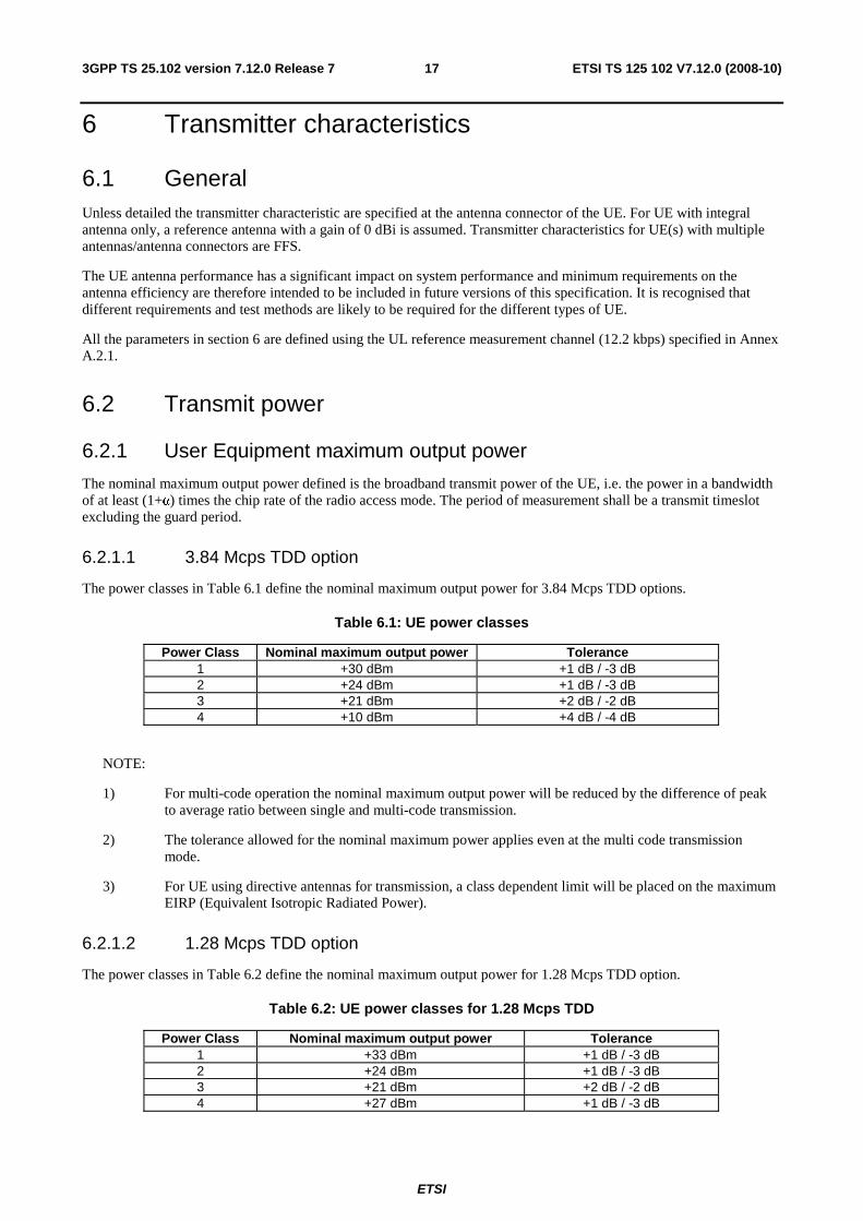
6 Transmitter characteristics
6.1 General Unless detailed the transmitter characteristic are specified at the antenna connector of the UE. For UE with integral antenna only, a reference antenna with a gain of 0 dBi is assumed. Transmitter characteristics for UE(s) with multiple antennas/antenna connectors are FFS.
The UE antenna performance has a significant impact on system performance and minimum requirements on the antenna efficiency are therefore intended to be included in future versions of this specification. It is recognised that different requirements and test methods are likely to be required for the different types of UE.
All the parameters in section 6 are defined using the UL reference measurement channel (12.2 kbps) specified in Annex A.2.1.
6.2 Transmit power
6.2.1 User Equipment maximum output power
The nominal maximum output power defined is the broadband transmit power of the UE, i.e. the power in a bandwidth of at least (1+α) times the chip rate of the radio access mode. The period of measurement shall be a transmit timeslot excluding the guard period.
6.2.1.1 3.84 Mcps TDD option
The power classes in Table 6.1 define the nominal maximum output power for 3.84 Mcps TDD options.
Table 6.1: UE power classes
Power Class Nominal maximum output power Tolerance 1 +30 dBm +1 dB / -3 dB 2 +24 dBm +1 dB / -3 dB 3 +21 dBm +2 dB / -2 dB 4 +10 dBm +4 dB / -4 dB
NOTE:
1) For multi-code operation the nominal maximum output power will be reduced by the difference of peak to average ratio between single and multi-code transmission.
2) The tolerance allowed for the nominal maximum power applies even at the multi code transmission mode.
3) For UE using directive antennas for transmission, a class dependent limit will be placed on the maximum EIRP (Equivalent Isotropic Radiated Power).
6.2.1.2 1.28 Mcps TDD option
The power classes in Table 6.2 define the nominal maximum output power for 1.28 Mcps TDD option.
Table 6.2: UE power classes for 1.28 Mcps TDD
Power Class Nominal maximum output power Tolerance 1 +33 dBm +1 dB / -3 dB 2 +24 dBm +1 dB / -3 dB 3 +21 dBm +2 dB / -2 dB 4 +27 dBm +1 dB / -3 dB

ETSI
ETSI TS 125 102 V7.12.0 (2008-10) 183GPP TS 25.102 version 7.12.0 Release 7
NOTE 1: For multi-code operation the nominal maximum output power will be reduced by the difference of peak to average ratio between single and multi-code transmission.
NOTE 2: The tolerance allowed for the nominal maximum power applies even at the multi code transmission mode.
NOTE 3: For UE using directive antennas for transmission, a class dependent limit will be placed on the maximum EIRP (Equivalent Isotropic Radiated Power).
6.2.1.3 7.68 Mcps TDD option
The power classes in Table 6.1 define the nominal maximum output power for 7.68 Mcps TDD options.
Table 6.3: UE power classes
Power Class Nominal maximum output power Tolerance 1 +30 dBm +1 dB / -3 dB 2 +24 dBm +1 dB / -3 dB 3 +21 dBm +2 dB / -2 dB 4 +10 dBm +4 dB / -4 dB
NOTE 1: For multi-code operation the nominal maximum output power will be reduced by the difference of peak to average ratio between single and multi-code transmission.
NOTE 2: The tolerance allowed for the nominal maximum power applies even at the multi code transmission mode.
NOTE 3: For UE using directive antennas for transmission, a class dependent limit will be placed on the maximum EIRP (Equivalent Isotropic Radiated Power).
6.3 UE frequency stability
The UE modulated carrier frequency shall be accurate to within ±0.1 PPM observed over a period of one timeslot compared to carrier frequency received from the BS. These signals will have an apparent error due to BS frequency error and Doppler shift. In the later case, signals from the BS must be averaged over sufficient time that errors due to noise or interference are allowed for within the above ±0.1PPM figure. The UE shall use the same frequency source for both RF frequency generation and the chip clock.
6.4 Output power dynamics Power control is used to limit the interference level.
6.4.1 Power control
6.4.1.1 3.84 Mcps option
Uplink power control is the ability of the UE transmitter to sets its output power in accordance with measured downlink path loss, values determined by higher layer signalling and path loss weighting parameter α as defined in TS 25.331. The output power is defined as the RRC filtered mean power of the transmit timeslot.
6.4.1.1.1 Initial Accuracy
The UE power control initial accuracy error shall be less than +/-9dB under normal conditions and +/- 12dB under extreme conditions.
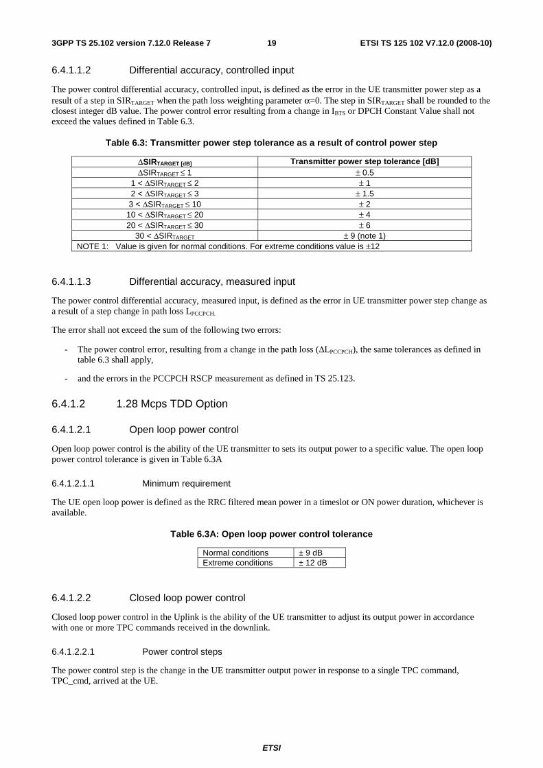
ETSI
ETSI TS 125 102 V7.12.0 (2008-10) 193GPP TS 25.102 version 7.12.0 Release 7
6.4.1.1.2 Differential accuracy, controlled input
The power control differential accuracy, controlled input, is defined as the error in the UE transmitter power step as a result of a step in SIRTARGET when the path loss weighting parameter α=0. The step in SIRTARGET shall be rounded to the closest integer dB value. The power control error resulting from a change in IBTS or DPCH Constant Value shall not exceed the values defined in Table 6.3.
Table 6.3: Transmitter power step tolerance as a result of control power step
ΔSIRTARGET [dB] Transmitter power step tolerance [dB] ΔSIRTARGET ≤ 1 ± 0.5
1 < ΔSIRTARGET ≤ 2 ± 1 2 < ΔSIRTARGET ≤ 3 ± 1.5 3 < ΔSIRTARGET ≤ 10 ± 2
10 < ΔSIRTARGET ≤ 20 ± 4 20 < ΔSIRTARGET ≤ 30 ± 6
30 < ΔSIRTARGET ± 9 (note 1)
NOTE 1: Value is given for normal conditions. For extreme conditions value is ±12
6.4.1.1.3 Differential accuracy, measured input
The power control differential accuracy, measured input, is defined as the error in UE transmitter power step change as a result of a step change in path loss LPCCPCH.
The error shall not exceed the sum of the following two errors:
- The power control error, resulting from a change in the path loss (ΔLPCCPCH), the same tolerances as defined in table 6.3 shall apply,
- and the errors in the PCCPCH RSCP measurement as defined in TS 25.123.
6.4.1.2 1.28 Mcps TDD Option
6.4.1.2.1 Open loop power control
Open loop power control is the ability of the UE transmitter to sets its output power to a specific value. The open loop power control tolerance is given in Table 6.3A
6.4.1.2.1.1 Minimum requirement
The UE open loop power is defined as the RRC filtered mean power in a timeslot or ON power duration, whichever is available.
Table 6.3A: Open loop power control tolerance
Normal conditions ± 9 dB Extreme conditions ± 12 dB
6.4.1.2.2 Closed loop power control
Closed loop power control in the Uplink is the ability of the UE transmitter to adjust its output power in accordance with one or more TPC commands received in the downlink.
6.4.1.2.2.1 Power control steps
The power control step is the change in the UE transmitter output power in response to a single TPC command, TPC_cmd, arrived at the UE.

ETSI
ETSI TS 125 102 V7.12.0 (2008-10) 203GPP TS 25.102 version 7.12.0 Release 7
6.4.1.2.2.1.1 Minimum requirement
The UE transmitter shall have the capability of changing the output power with a step size of 1, 2 and 3 dB according to the value of ΔTPC or ΔRP-TPC, in the slot immediately after the TPC_cmd can be arrived.
a) The transmitter output power step due to closed loop power control shall be within the range shown in Table 6.3B.
b) The transmitter average output power step due to closed loop power control shall be within the range shown in Table 6.3C. Here a TPC_cmd group is a set of TPC_cmd values derived from a corresponding sequence of TPC commands of the same duration.
The closed loop power is defined as the relative power differences between RRC filtered mean power of original (reference) timeslot and RRC filtered mean power of the target timeslot without transient duration.
Table 6.3B: Transmitter power control range
Transmitter power control range 1 dB step size 2 dB step size 3 dB step size TPC_cmd
Lower Upper Lower Upper Lower Upper
Up +0.5 dB +1.5 dB +1 dB +3 dB +1.5 dB +4.5 dB Down -0.5 dB -1.5 dB -1 dB -3 dB -1.5 dB -4.5 dB
Table 6.3C: Transmitter average power control range
Transmitter power control range after 10 equal TPC_ cmd groups 1 dB step size 2 dB step size 3 dB step size TPC_cmd group
Lower Upper Lower Upper Lower Upper Up +8 dB +12 dB +16 dB +24 dB +24 dB +36 dB
Down -8 dB -12 dB -16 dB -24 dB -24 dB -36 dB
6.4.1.3 7.68 Mcps option
Uplink power control is the ability of the UE transmitter to sets its output power in accordance with measured downlink path loss, values determined by higher layer signalling and path loss weighting parameter α as defined in TS 25.331. The output power is defined as the RRC filtered mean power of the transmit timeslot.
6.4.1.3.1 Initial Accuracy
The UE power control initial accuracy error shall be less than +/-9dB under normal conditions and +/- 12dB under extreme conditions.
6.4.1.3.2 Differential accuracy, controlled input
The power control differential accuracy, controlled input, is defined as the error in the UE transmitter power step as a result of a step in SIRTARGET when the path loss weighting parameter α=0. The step in SIRTARGET shall be rounded to the closest integer dB value. The power control error resulting from a change in IBTS or DPCH Constant Value shall not exceed the values defined in Table 6.3D.
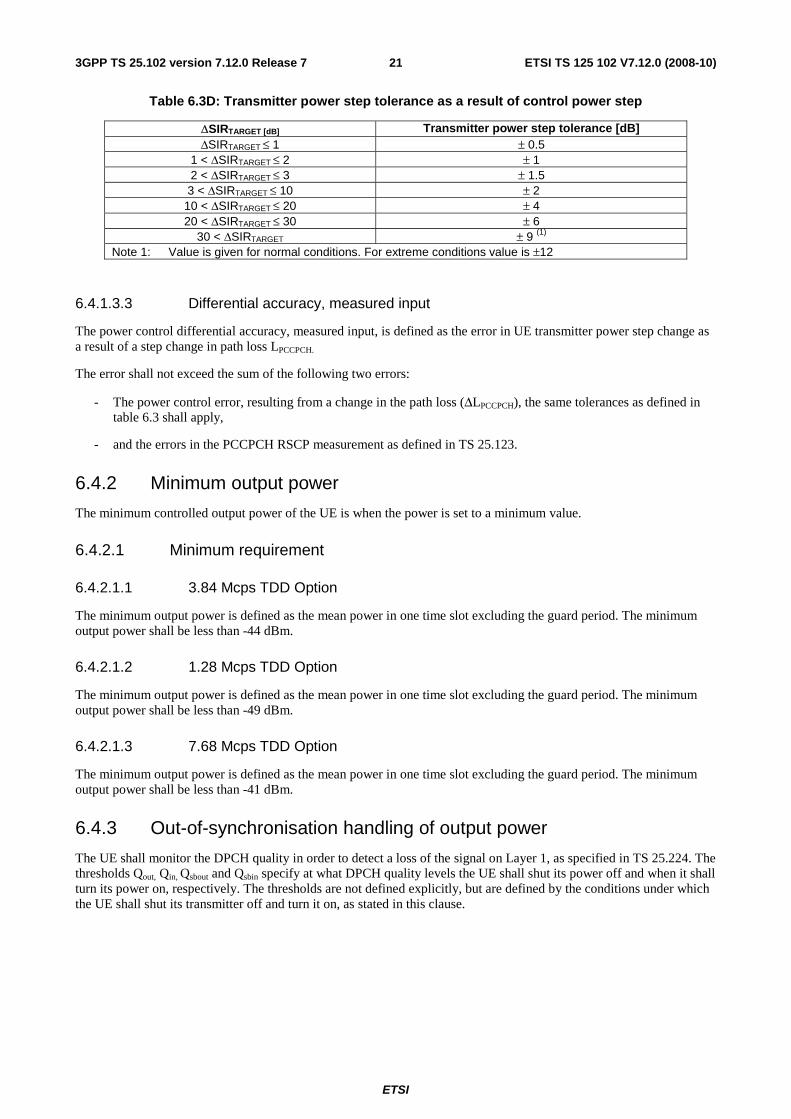
ETSI
ETSI TS 125 102 V7.12.0 (2008-10) 213GPP TS 25.102 version 7.12.0 Release 7
Table 6.3D: Transmitter power step tolerance as a result of control power step
ΔSIRTARGET [dB] Transmitter power step tolerance [dB] ΔSIRTARGET ≤ 1 ± 0.5
1 < ΔSIRTARGET ≤ 2 ± 1 2 < ΔSIRTARGET ≤ 3 ± 1.5 3 < ΔSIRTARGET ≤ 10 ± 2
10 < ΔSIRTARGET ≤ 20 ± 4 20 < ΔSIRTARGET ≤ 30 ± 6
30 < ΔSIRTARGET ± 9 (1)
Note 1: Value is given for normal conditions. For extreme conditions value is ±12
6.4.1.3.3 Differential accuracy, measured input
The power control differential accuracy, measured input, is defined as the error in UE transmitter power step change as a result of a step change in path loss LPCCPCH.
The error shall not exceed the sum of the following two errors:
- The power control error, resulting from a change in the path loss (ΔLPCCPCH), the same tolerances as defined in table 6.3 shall apply,
- and the errors in the PCCPCH RSCP measurement as defined in TS 25.123.
6.4.2 Minimum output power
The minimum controlled output power of the UE is when the power is set to a minimum value.
6.4.2.1 Minimum requirement
6.4.2.1.1 3.84 Mcps TDD Option
The minimum output power is defined as the mean power in one time slot excluding the guard period. The minimum output power shall be less than -44 dBm.
6.4.2.1.2 1.28 Mcps TDD Option
The minimum output power is defined as the mean power in one time slot excluding the guard period. The minimum output power shall be less than -49 dBm.
6.4.2.1.3 7.68 Mcps TDD Option
The minimum output power is defined as the mean power in one time slot excluding the guard period. The minimum output power shall be less than -41 dBm.
6.4.3 Out-of-synchronisation handling of output power
The UE shall monitor the DPCH quality in order to detect a loss of the signal on Layer 1, as specified in TS 25.224. The thresholds Qout, Qin, Qsbout and Qsbin specify at what DPCH quality levels the UE shall shut its power off and when it shall turn its power on, respectively. The thresholds are not defined explicitly, but are defined by the conditions under which the UE shall shut its transmitter off and turn it on, as stated in this clause.
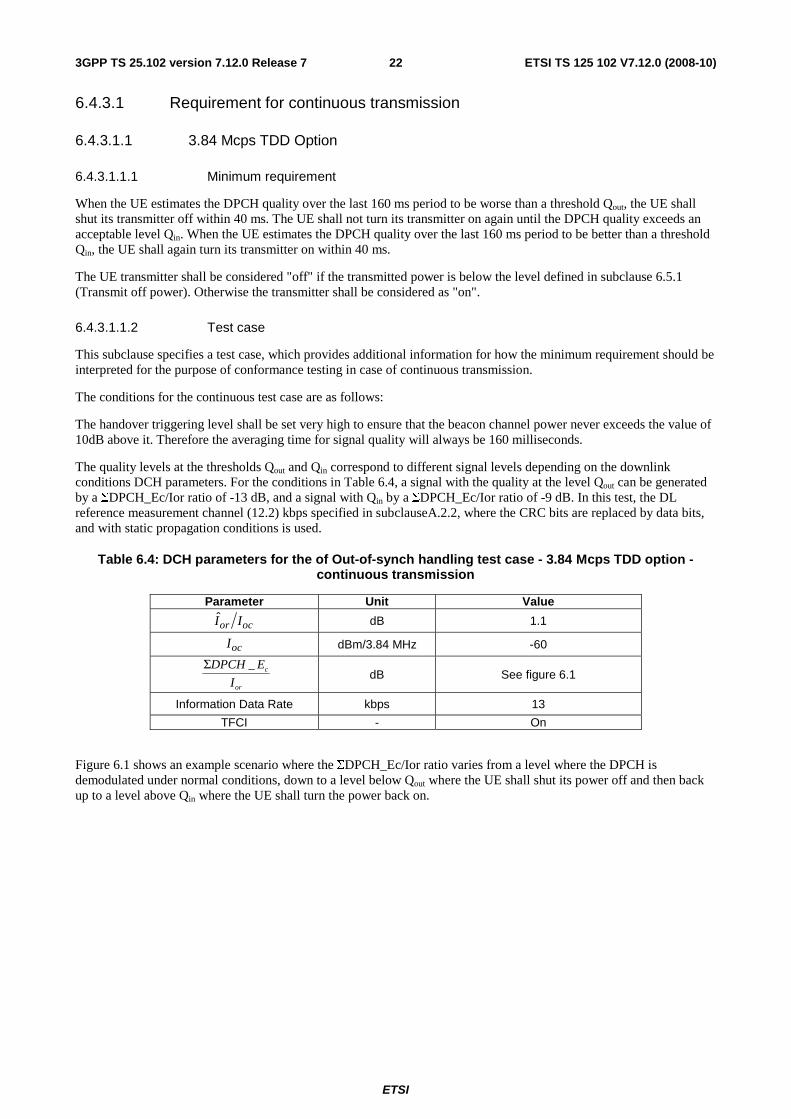
ETSI
ETSI TS 125 102 V7.12.0 (2008-10) 223GPP TS 25.102 version 7.12.0 Release 7
6.4.3.1 Requirement for continuous transmission
6.4.3.1.1 3.84 Mcps TDD Option
6.4.3.1.1.1 Minimum requirement
When the UE estimates the DPCH quality over the last 160 ms period to be worse than a threshold Qout, the UE shall shut its transmitter off within 40 ms. The UE shall not turn its transmitter on again until the DPCH quality exceeds an acceptable level Qin. When the UE estimates the DPCH quality over the last 160 ms period to be better than a threshold Qin, the UE shall again turn its transmitter on within 40 ms.
The UE transmitter shall be considered "off" if the transmitted power is below the level defined in subclause 6.5.1 (Transmit off power). Otherwise the transmitter shall be considered as "on".
6.4.3.1.1.2 Test case
This subclause specifies a test case, which provides additional information for how the minimum requirement should be interpreted for the purpose of conformance testing in case of continuous transmission.
The conditions for the continuous test case are as follows:
The handover triggering level shall be set very high to ensure that the beacon channel power never exceeds the value of 10dB above it. Therefore the averaging time for signal quality will always be 160 milliseconds.
The quality levels at the thresholds Qout and Qin correspond to different signal levels depending on the downlink conditions DCH parameters. For the conditions in Table 6.4, a signal with the quality at the level Qout can be generated by a ΣDPCH_Ec/Ior ratio of -13 dB, and a signal with Qin by a ΣDPCH_Ec/Ior ratio of -9 dB. In this test, the DL reference measurement channel (12.2) kbps specified in subclauseA.2.2, where the CRC bits are replaced by data bits, and with static propagation conditions is used.
Table 6.4: DCH parameters for the of Out-of-synch handling test case - 3.84 Mcps TDD option - continuous transmission
Parameter Unit Value
ocor II dB 1.1
ocI dBm/3.84 MHz -60
or
c
I
EDPCH _Σ dB See figure 6.1
Information Data Rate kbps 13
TFCI - On
Figure 6.1 shows an example scenario where the ΣDPCH_Ec/Ior ratio varies from a level where the DPCH is demodulated under normal conditions, down to a level below Qout where the UE shall shut its power off and then back up to a level above Qin where the UE shall turn the power back on.
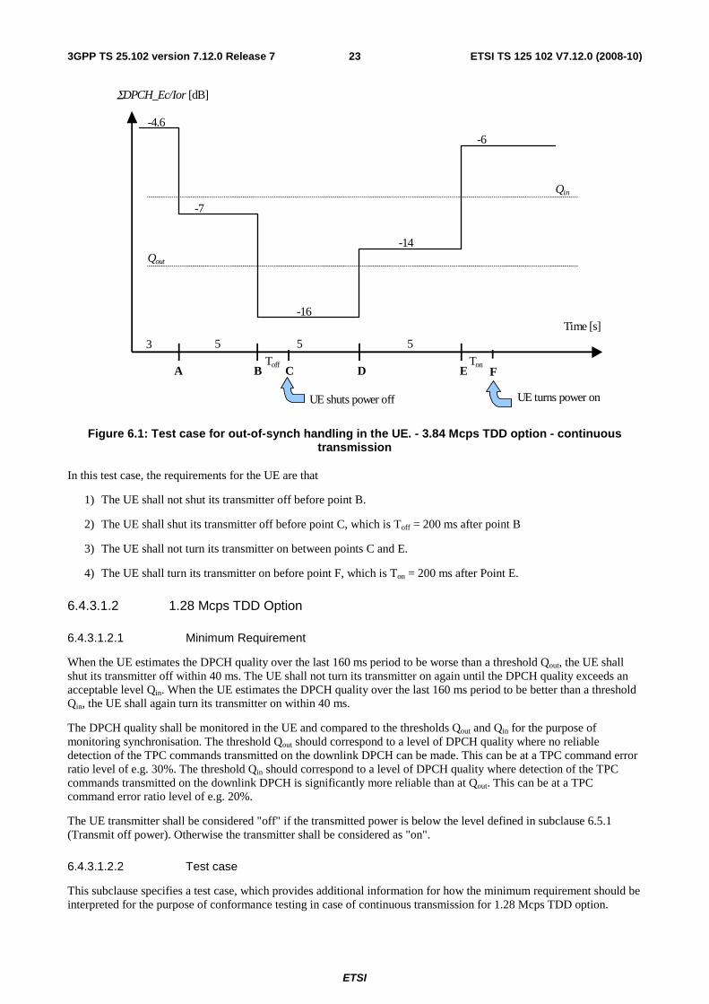
ETSI
ETSI TS 125 102 V7.12.0 (2008-10) 233GPP TS 25.102 version 7.12.0 Release 7
ΣDPCH_Ec/Ior [dB]
A B C D E
Time [s]
-4.6
-7
-16
-14
-6
UE shuts power off UE turns power on
5
Toff
5
Qout
Qin
5
F
3 Ton
Figure 6.1: Test case for out-of-synch handling in the UE. - 3.84 Mcps TDD option - continuous transmission
In this test case, the requirements for the UE are that
1) The UE shall not shut its transmitter off before point B.
2) The UE shall shut its transmitter off before point C, which is Toff = 200 ms after point B
3) The UE shall not turn its transmitter on between points C and E.
4) The UE shall turn its transmitter on before point F, which is Ton = 200 ms after Point E.
6.4.3.1.2 1.28 Mcps TDD Option
6.4.3.1.2.1 Minimum Requirement
When the UE estimates the DPCH quality over the last 160 ms period to be worse than a threshold Qout, the UE shall shut its transmitter off within 40 ms. The UE shall not turn its transmitter on again until the DPCH quality exceeds an acceptable level Qin. When the UE estimates the DPCH quality over the last 160 ms period to be better than a threshold Qin, the UE shall again turn its transmitter on within 40 ms.
The DPCH quality shall be monitored in the UE and compared to the thresholds Qout and Qin for the purpose of monitoring synchronisation. The threshold Qout should correspond to a level of DPCH quality where no reliable detection of the TPC commands transmitted on the downlink DPCH can be made. This can be at a TPC command error ratio level of e.g. 30%. The threshold Qin should correspond to a level of DPCH quality where detection of the TPC commands transmitted on the downlink DPCH is significantly more reliable than at Qout. This can be at a TPC command error ratio level of e.g. 20%.
The UE transmitter shall be considered "off" if the transmitted power is below the level defined in subclause 6.5.1 (Transmit off power). Otherwise the transmitter shall be considered as "on".
6.4.3.1.2.2 Test case
This subclause specifies a test case, which provides additional information for how the minimum requirement should be interpreted for the purpose of conformance testing in case of continuous transmission for 1.28 Mcps TDD option.

ETSI
ETSI TS 125 102 V7.12.0 (2008-10) 243GPP TS 25.102 version 7.12.0 Release 7
The conditions for the continuous test case are as follows:
The handover triggering level shall be set very high to ensure that the beacon channel power never exceeds the value of 10dB above it. Therefore the averaging time for signal quality will always be 160 milliseconds.
The quality levels at the thresholds Qout and Qin correspond to different signal levels depending on the downlink conditions DCH parameters. For the conditions in Table 6.4, a signal with the quality at the level Qout can be generated by a ΣDPCH_Ec/Ior ratio of -15 dB, and a signal with Qin by a ΣDPCH_Ec/Ior ratio of -4.5 dB. In this test, the DL reference measurement channel (12.2) kbps specified in subclause A.2.2, where the CRC bits are replaced by data bits, and with static propagation conditions is used.
Table 6.4AA: DCH parameters for the of Out-of-synch handling test case - 1.28 Mcps TDD option - continuous transmission
Parameter Unit Value
ocor II dB -1
ocI dBm/1.28 MHz -60
or
c
I
EDPCH _Σ dB See figure 6.1AA
Information Data Rate kbps 12.2
TFCI - On
Figure 6.1AA shows an example scenario where the ΣDPCH_Ec/Ior ratio varies from a level where the DPCH is demodulated under normal conditions, down to a level below Qout where the UE shall shut its power off and then back up to a level above Qin where the UE shall turn the power back on.
ΣDPCH_Ec/Ior [dB]
A B C D E F
Time [s]
-6
UE shuts power off UE turns power on
5 T off
Qout
Qin
-2.4
-14
-16
-3
T on 0
5 5 3
Figure 6.1AA: Test case for out-of-synch handling in the UE - 1.28 Mcps TDD option - continuous transmission

ETSI
ETSI TS 125 102 V7.12.0 (2008-10) 253GPP TS 25.102 version 7.12.0 Release 7
In this test case, the requirements for the UE are that:
1) The UE shall not shut its transmitter off before point B.
2) The UE shall shut its transmitter off before point C, which is Toff = 200 ms after point B
3) The UE shall not turn its transmitter on between points C and E.
4) The UE shall turn its transmitter on before point F, which is Ton = 200 ms after Point E.
6.4.3.1.3 7.68 Mcps TDD Option
6.4.3.1.3.1 Minimum requirement
When the UE estimates the DPCH quality over the last 160 ms period to be worse than a threshold Qout, the UE shall shut its transmitter off within 40 ms. The UE shall not turn its transmitter on again until the DPCH quality exceeds an acceptable level Qin. When the UE estimates the DPCH quality over the last 160 ms period to be better than a threshold Qin, the UE shall again turn its transmitter on within 40 ms.
The UE transmitter shall be considered "off" if the transmitted power is below the level defined in subclause 6.5.1 (Transmit off power). Otherwise the transmitter shall be considered as "on".
6.4.3.1.3.2 Test case
This subclause specifies a test case, which provides additional information for how the minimum requirement should be interpreted for the purpose of conformance testing in case of continuous transmission.
The conditions for the continuous test case are as follows:
The handover triggering level shall be set very high to ensure that the beacon channel power never exceeds the value of 10dB above it. Therefore the averaging time for signal quality will always be 160 milliseconds.
The quality levels at the thresholds Qout and Qin correspond to different signal levels depending on the downlink conditions DCH parameters. For the conditions in Table 6.4AB, a signal with the quality at the level Qout can be generated by a ΣDPCH_Ec/Ior ratio of -16 dB, and a signal with Qin by a ΣDPCH_Ec/Ior ratio of -12 dB. In this test, the DL reference measurement channel (12.2) kbps specified in subclause A.2.2, where the CRC bits are replaced by data bits, and with static propagation conditions is used.
Table 6.4AB: DCH parameters for the of Out-of-synch handling test case - 7.68 Mcps TDD option - continuous transmission
Parameter Unit Value
ocor II dB 1.1
ocI dBm/7.68 MHz -60
or
c
I
EDPCH _Σ dB See Figure 6.1BB
Information Data Rate kbps 13
TFCI - On
Figure 6.1AB shows an example scenario where the ΣDPCH_Ec/Ior ratio varies from a level where the DPCH is demodulated under normal conditions, down to a level below Qout where the UE shall shut its power off and then back up to a level above Qin where the UE shall turn the power back on.
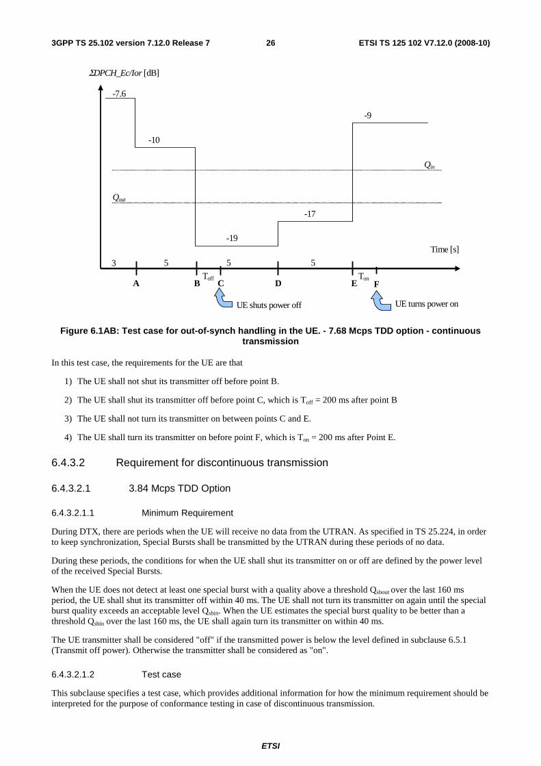
ETSI
ETSI TS 125 102 V7.12.0 (2008-10) 263GPP TS 25.102 version 7.12.0 Release 7
ΣDPCH_Ec/Ior [dB]
A B C D E
Time [s]
-7.6
-10
-19
-17
-9
UE shuts power off UE turns power on
5
Toff
5
Qout
Qin
5
F
3
Ton
Figure 6.1AB: Test case for out-of-synch handling in the UE. - 7.68 Mcps TDD option - continuous transmission
In this test case, the requirements for the UE are that
1) The UE shall not shut its transmitter off before point B.
2) The UE shall shut its transmitter off before point C, which is Toff = 200 ms after point B
3) The UE shall not turn its transmitter on between points C and E.
4) The UE shall turn its transmitter on before point F, which is Ton = 200 ms after Point E.
6.4.3.2 Requirement for discontinuous transmission
6.4.3.2.1 3.84 Mcps TDD Option
6.4.3.2.1.1 Minimum Requirement
During DTX, there are periods when the UE will receive no data from the UTRAN. As specified in TS 25.224, in order to keep synchronization, Special Bursts shall be transmitted by the UTRAN during these periods of no data.
During these periods, the conditions for when the UE shall shut its transmitter on or off are defined by the power level of the received Special Bursts.
When the UE does not detect at least one special burst with a quality above a threshold Qsbout over the last 160 ms period, the UE shall shut its transmitter off within 40 ms. The UE shall not turn its transmitter on again until the special burst quality exceeds an acceptable level Qsbin. When the UE estimates the special burst quality to be better than a threshold Qsbin over the last 160 ms, the UE shall again turn its transmitter on within 40 ms.
The UE transmitter shall be considered "off" if the transmitted power is below the level defined in subclause 6.5.1 (Transmit off power). Otherwise the transmitter shall be considered as "on".
6.4.3.2.1.2 Test case
This subclause specifies a test case, which provides additional information for how the minimum requirement should be interpreted for the purpose of conformance testing in case of discontinuous transmission.
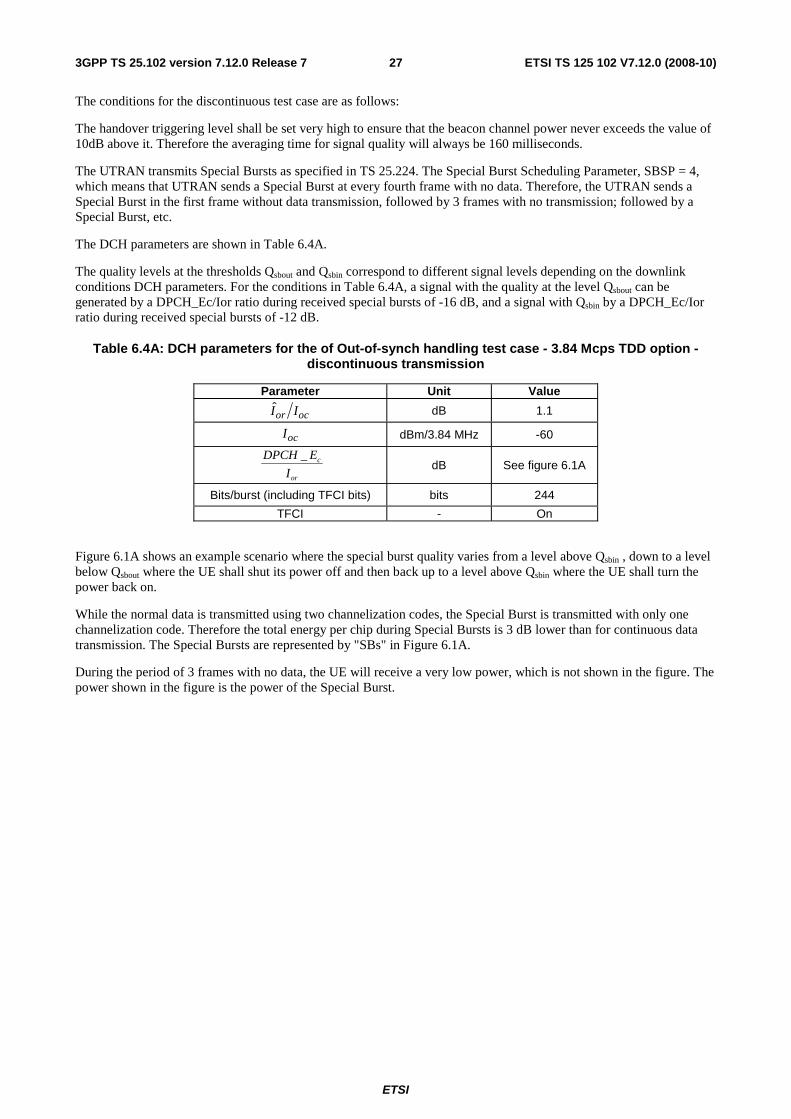
ETSI
ETSI TS 125 102 V7.12.0 (2008-10) 273GPP TS 25.102 version 7.12.0 Release 7
The conditions for the discontinuous test case are as follows:
The handover triggering level shall be set very high to ensure that the beacon channel power never exceeds the value of 10dB above it. Therefore the averaging time for signal quality will always be 160 milliseconds.
The UTRAN transmits Special Bursts as specified in TS 25.224. The Special Burst Scheduling Parameter, SBSP = 4, which means that UTRAN sends a Special Burst at every fourth frame with no data. Therefore, the UTRAN sends a Special Burst in the first frame without data transmission, followed by 3 frames with no transmission; followed by a Special Burst, etc.
The DCH parameters are shown in Table 6.4A.
The quality levels at the thresholds Qsbout and Qsbin correspond to different signal levels depending on the downlink conditions DCH parameters. For the conditions in Table 6.4A, a signal with the quality at the level Qsbout can be generated by a DPCH_Ec/Ior ratio during received special bursts of -16 dB, and a signal with Qsbin by a DPCH_Ec/Ior ratio during received special bursts of -12 dB.
Table 6.4A: DCH parameters for the of Out-of-synch handling test case - 3.84 Mcps TDD option - discontinuous transmission
Parameter Unit Value
ocor II dB 1.1
ocI dBm/3.84 MHz -60
or
c
I
EDPCH _ dB See figure 6.1A
Bits/burst (including TFCI bits) bits 244
TFCI - On
Figure 6.1A shows an example scenario where the special burst quality varies from a level above Qsbin , down to a level below Qsbout where the UE shall shut its power off and then back up to a level above Qsbin where the UE shall turn the power back on.
While the normal data is transmitted using two channelization codes, the Special Burst is transmitted with only one channelization code. Therefore the total energy per chip during Special Bursts is 3 dB lower than for continuous data transmission. The Special Bursts are represented by "SBs" in Figure 6.1A.
During the period of 3 frames with no data, the UE will receive a very low power, which is not shown in the figure. The power shown in the figure is the power of the Special Burst.
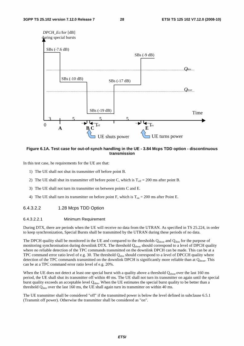
ETSI
ETSI TS 125 102 V7.12.0 (2008-10) 283GPP TS 25.102 version 7.12.0 Release 7
DPCH_Ec/Ior [dB] during special bursts
A B C D
E F
Time [s]
UE shuts power off
UE turns power on
T of f
Q sbo ut
Q sbi n
T on 0 5 5 3 5
SBs (-7.6 dB) SBs (-9 dB)
SBs (-10 dB) SBs (-17 dB)
SBs (-19 dB)
Figure 6.1A. Test case for out-of-synch handling in the UE - 3.84 Mcps TDD option - discontinuous transmission
In this test case, he requirements for the UE are that:
1) The UE shall not shut its transmitter off before point B.
2) The UE shall shut its transmitter off before point C, which is Toff = 200 ms after point B.
3) The UE shall not turn its transmitter on between points C and E.
4) The UE shall turn its transmitter on before point F, which is Ton = 200 ms after Point E.
6.4.3.2.2 1.28 Mcps TDD Option
6.4.3.2.2.1 Minimum Requirement
During DTX, there are periods when the UE will receive no data from the UTRAN. As specified in TS 25.224, in order to keep synchronization, Special Bursts shall be transmitted by the UTRAN during these periods of no data.
The DPCH quality shall be monitored in the UE and compared to the thresholds Qsbout and Qsbin for the purpose of monitoring synchronisation during downlink DTX. The threshold Qsbout should correspond to a level of DPCH quality where no reliable detection of the TPC commands transmitted on the downlink DPCH can be made. This can be at a TPC command error ratio level of e.g. 30. The threshold Qsbin should correspond to a level of DPCCH quality where detection of the TPC commands transmitted on the downlink DPCH is significantly more reliable than at Qsbout. This can be at a TPC command error ratio level of e.g. 20%.
When the UE does not detect at least one special burst with a quality above a threshold Qsbout over the last 160 ms period, the UE shall shut its transmitter off within 40 ms. The UE shall not turn its transmitter on again until the special burst quality exceeds an acceptable level Qsbin. When the UE estimates the special burst quality to be better than a threshold Qsbin over the last 160 ms, the UE shall again turn its transmitter on within 40 ms.
The UE transmitter shall be considered "off" if the transmitted power is below the level defined in subclause 6.5.1 (Transmit off power). Otherwise the transmitter shall be considered as "on".
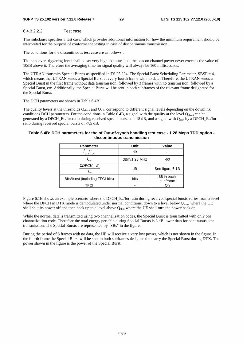
ETSI
ETSI TS 125 102 V7.12.0 (2008-10) 293GPP TS 25.102 version 7.12.0 Release 7
6.4.3.2.2.2 Test case
This subclause specifies a test case, which provides additional information for how the minimum requirement should be interpreted for the purpose of conformance testing in case of discontinuous transmission.
The conditions for the discontinuous test case are as follows :
The handover triggering level shall be set very high to ensure that the beacon channel power never exceeds the value of 10dB above it. Therefore the averaging time for signal quality will always be 160 milliseconds.
The UTRAN transmits Special Bursts as specified in TS 25.224. The Special Burst Scheduling Parameter, SBSP = 4, which means that UTRAN sends a Special Burst at every fourth frame with no data. Therefore, the UTRAN sends a Special Burst in the first frame without data transmission, followed by 3 frames with no transmission; followed by a Special Burst, etc. Additionally, the Special Burst will be sent in both subframes of the relevant frame designated for the Special Burst.
The DCH parameters are shown in Table 6.4B.
The quality levels at the thresholds Qsbout and Qsbin correspond to different signal levels depending on the downlink conditions DCH parameters. For the conditions in Table 6.4B, a signal with the quality at the level Qsbout can be generated by a DPCH_Ec/Ior ratio during received special bursts of -18 dB, and a signal with Qsbin by a DPCH_Ec/Ior ratio during received special bursts of -7,5 dB.
Table 6.4B: DCH parameters for the of Out-of-synch handling test case - 1.28 Mcps TDD option - discontinuous transmission
Parameter Unit Value
ocor II dB -1
ocI dBm/1.28 MHz -60
or
c
I
EDPCH _Σ dB See figure 6.1B
Bits/burst (including TFCI bits) bits 88 in each subframe
TFCI - On
Figure 6.1B shows an example scenario where the DPCH_Ec/Ior ratio during received special bursts varies from a level where the DPCH in DTX mode is demodulated under normal conditions, down to a level below Qsbout where the UE shall shut its power off and then back up to a level above Qsbin where the UE shall turn the power back on.
While the normal data is transmitted using two channelization codes, the Special Burst is transmitted with only one channelization code. Therefore the total energy per chip during Special Bursts is 3 dB lower than for continuous data transmission. The Special Bursts are represented by "SBs" in the figure.
During the period of 3 frames with no data, the UE will receive a very low power, which is not shown in the figure. In the fourth frame the Special Burst will be sent in both subframes designated to carry the Special Burst during DTX. The power shown in the figure is the power of the Special Burst.
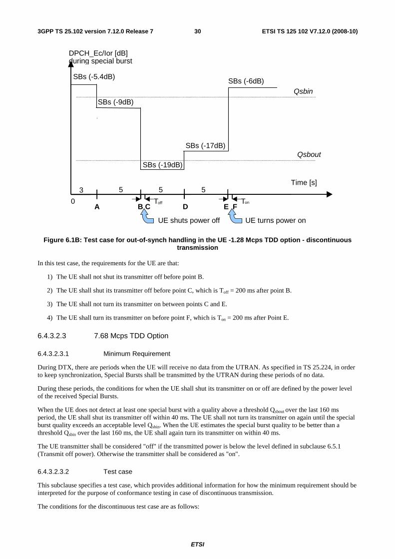
ETSI
ETSI TS 125 102 V7.12.0 (2008-10) 303GPP TS 25.102 version 7.12.0 Release 7
DPCH_Ec/Ior [dB] during special burst
A B C D E F
Time [s]
SBs (-9dB)
UE shuts power off UE turns power on
5
T off
Qsbout
Qsbin
3
SBs (-5.4dB)
SBs (-17dB)
SBs (-19dB)
SBs (-6dB)
T on 0
5 5
Figure 6.1B: Test case for out-of-synch handling in the UE -1.28 Mcps TDD option - discontinuous transmission
In this test case, the requirements for the UE are that:
1) The UE shall not shut its transmitter off before point B.
2) The UE shall shut its transmitter off before point C, which is Toff = 200 ms after point B.
3) The UE shall not turn its transmitter on between points C and E.
4) The UE shall turn its transmitter on before point F, which is Ton = 200 ms after Point E.
6.4.3.2.3 7.68 Mcps TDD Option
6.4.3.2.3.1 Minimum Requirement
During DTX, there are periods when the UE will receive no data from the UTRAN. As specified in TS 25.224, in order to keep synchronization, Special Bursts shall be transmitted by the UTRAN during these periods of no data.
During these periods, the conditions for when the UE shall shut its transmitter on or off are defined by the power level of the received Special Bursts.
When the UE does not detect at least one special burst with a quality above a threshold Qsbout over the last 160 ms period, the UE shall shut its transmitter off within 40 ms. The UE shall not turn its transmitter on again until the special burst quality exceeds an acceptable level Qsbin. When the UE estimates the special burst quality to be better than a threshold Qsbin over the last 160 ms, the UE shall again turn its transmitter on within 40 ms.
The UE transmitter shall be considered "off" if the transmitted power is below the level defined in subclause 6.5.1 (Transmit off power). Otherwise the transmitter shall be considered as "on".
6.4.3.2.3.2 Test case
This subclause specifies a test case, which provides additional information for how the minimum requirement should be interpreted for the purpose of conformance testing in case of discontinuous transmission.
The conditions for the discontinuous test case are as follows:
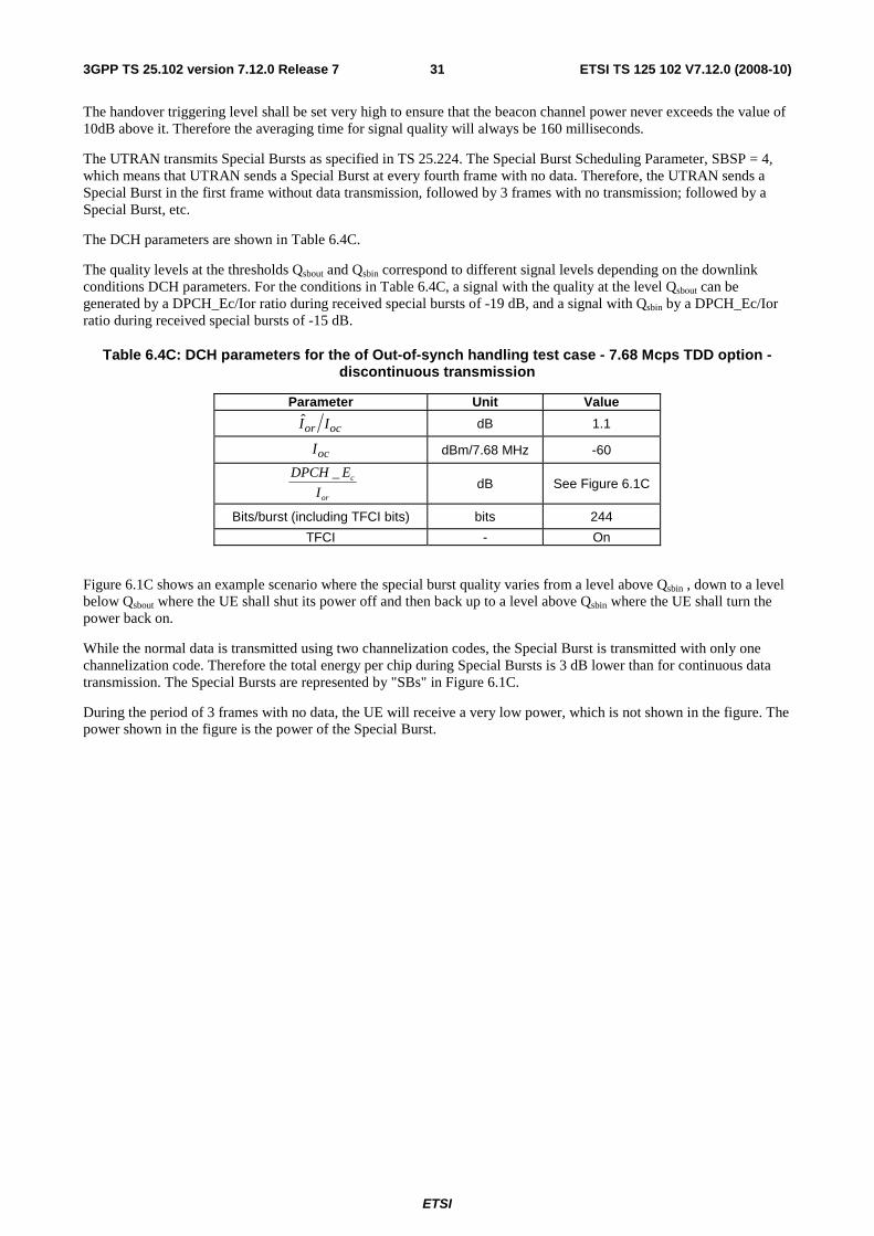
ETSI
ETSI TS 125 102 V7.12.0 (2008-10) 313GPP TS 25.102 version 7.12.0 Release 7
The handover triggering level shall be set very high to ensure that the beacon channel power never exceeds the value of 10dB above it. Therefore the averaging time for signal quality will always be 160 milliseconds.
The UTRAN transmits Special Bursts as specified in TS 25.224. The Special Burst Scheduling Parameter, SBSP = 4, which means that UTRAN sends a Special Burst at every fourth frame with no data. Therefore, the UTRAN sends a Special Burst in the first frame without data transmission, followed by 3 frames with no transmission; followed by a Special Burst, etc.
The DCH parameters are shown in Table 6.4C.
The quality levels at the thresholds Qsbout and Qsbin correspond to different signal levels depending on the downlink conditions DCH parameters. For the conditions in Table 6.4C, a signal with the quality at the level Qsbout can be generated by a DPCH_Ec/Ior ratio during received special bursts of -19 dB, and a signal with Qsbin by a DPCH_Ec/Ior ratio during received special bursts of -15 dB.
Table 6.4C: DCH parameters for the of Out-of-synch handling test case - 7.68 Mcps TDD option - discontinuous transmission
Parameter Unit Value
ocor II dB 1.1
ocI dBm/7.68 MHz -60
or
c
I
EDPCH _ dB See Figure 6.1C
Bits/burst (including TFCI bits) bits 244
TFCI - On
Figure 6.1C shows an example scenario where the special burst quality varies from a level above Qsbin , down to a level below Qsbout where the UE shall shut its power off and then back up to a level above Qsbin where the UE shall turn the power back on.
While the normal data is transmitted using two channelization codes, the Special Burst is transmitted with only one channelization code. Therefore the total energy per chip during Special Bursts is 3 dB lower than for continuous data transmission. The Special Bursts are represented by "SBs" in Figure 6.1C.
During the period of 3 frames with no data, the UE will receive a very low power, which is not shown in the figure. The power shown in the figure is the power of the Special Burst.
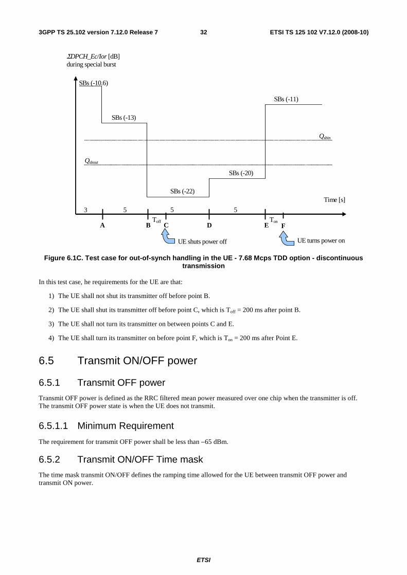
ETSI
ETSI TS 125 102 V7.12.0 (2008-10) 323GPP TS 25.102 version 7.12.0 Release 7
ΣDPCH_Ec/Ior [dB] during special burst
A B C D E
Time [s]
SBs (-10.6)
SBs (-13)
SBs (-22)
SBs (-20)
SBs (-11)
UE shuts power off UE turns power on
5
Toff
5
Qsbout
Qsbin
5
F
3
Ton
Figure 6.1C. Test case for out-of-synch handling in the UE - 7.68 Mcps TDD option - discontinuous transmission
In this test case, he requirements for the UE are that:
1) The UE shall not shut its transmitter off before point B.
2) The UE shall shut its transmitter off before point C, which is Toff = 200 ms after point B.
3) The UE shall not turn its transmitter on between points C and E.
4) The UE shall turn its transmitter on before point F, which is Ton = 200 ms after Point E.
6.5 Transmit ON/OFF power
6.5.1 Transmit OFF power
Transmit OFF power is defined as the RRC filtered mean power measured over one chip when the transmitter is off. The transmit OFF power state is when the UE does not transmit.
6.5.1.1 Minimum Requirement
The requirement for transmit OFF power shall be less than −65 dBm.
6.5.2 Transmit ON/OFF Time mask
The time mask transmit ON/OFF defines the ramping time allowed for the UE between transmit OFF power and transmit ON power.

ETSI
ETSI TS 125 102 V7.12.0 (2008-10) 333GPP TS 25.102 version 7.12.0 Release 7
6.5.2.1 Minimum Requirement
6.5.2.1.1 3.84 Mcps TDD Option
The transmit power level versus time shall meet the mask specified in figure 6.2, where the transmission period refers to the burst without guard period for a single transmission slot, and to the period from the beginning of the burst in the first transmission slot to the end of the burst without guard period in the last transmission timeslot for consecutive transmission slots.
96 chips Transmission period
Average ON Power
OFF Power
96chips50 chips-50 dBm
Figure 6.2: Transmit ON/OFF template for 3.84 Mcps TDD Option
6.5.2.1.2 1.28 Mcps TDD Option
The transmit power level versus time shall meet the mask specified in figure 6.2A, where the transmission period refers to the burst without guard period for a single transmission slot, and to the period from the beginning of the burst in the first transmission slot to the end of the burst without guard period in the last transmission timeslot for consecutive transmission slots.
13chips Transmission period
Average ON Power
OFF Power
12chips20 chips-50 dBm
Figure 6.2A: Transmit ON/OFF template for 1.28 Mcps TDD Option
6.5.2.1.3 7.68 Mcps TDD Option
The transmit power level versus time shall meet the mask specified in Figure 6.2B, where the transmission period refers to the burst without guard period for a single transmission slot, and to the period from the beginning of the burst in the first transmission slot to the end of the burst without guard period in the last transmission timeslot for consecutive transmission slots.

ETSI
ETSI TS 125 102 V7.12.0 (2008-10) 343GPP TS 25.102 version 7.12.0 Release 7
192 chips 100 chips 192 chips
Average ON Power
OFF Power
Transmission period -50 dBm
Figure 6.2B: Transmit ON/OFF template for 7.68 Mcps TDD Option
6.6 Output RF spectrum emissions
6.6.1 Occupied bandwidth
6.6.1.1 3.84 Mcps TDD Option
Occupied bandwidth is a measure of the bandwidth containing 99% of the total integrated power of the transmitted spectrum, centred on the assigned channel frequency. The occupied channel bandwidth shall be less than 5 MHz based on a chip rate of 3.84 Mcps.
6.6.1.2 1.28 Mcps TDD Option
Occupied bandwidth is a measure of the bandwidth containing 99% of the total integrated power of the transmitted spectrum, centred on the assigned channel frequency. The occupied channel bandwidth shall be less than 1.6 MHz based on a chip rate of 1.28 Mcps.
6.6.1.3 7.68 Mcps TDD Option
Occupied bandwidth is a measure of the bandwidth containing 99% of the total integrated power of the transmitted spectrum, centred on the assigned channel frequency. The occupied channel bandwidth shall be less than 10 MHz based on a chip rate of 7.68 Mcps.
6.6.2 Out of band emission
Out of band emissions are unwanted emissions immediately outside the nominal channel resulting from the modulation process and non-linearity in the transmitter but excluding spurious emissions. This out of band emission limit is specified in terms of a spectrum emission mask and adjacent channel leakage power ratio (ACLR).
6.6.2.1 Spectrum emission mask
6.6.2.1.1 3.84 Mcps TDD Option
The spectrum emission mask of the UE applies to frequencies, which are between 2.5 MHz and 12.5MHz from the UE centre carrier frequency. The out of channel emission is specified relative to theRRC filtered mean power of the UE carrier.
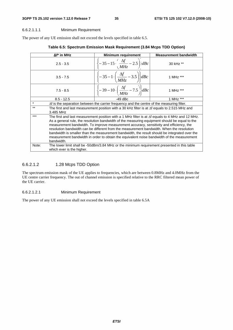
ETSI
ETSI TS 125 102 V7.12.0 (2008-10) 353GPP TS 25.102 version 7.12.0 Release 7
6.6.2.1.1.1 Minimum Requirement
The power of any UE emission shall not exceed the levels specified in table 6.5.
Table 6.5: Spectrum Emission Mask Requirement (3.84 Mcps TDD Option)
Δf* in MHz Minimum requirement Measurement bandwidth
2.5 - 3.5 dBcMHz
f
⎭⎬⎫
⎩⎨⎧
⎟⎠
⎞⎜⎝
⎛ −Δ⋅−− 5.21535 30 kHz **
3.5 - 7.5 dBcMHz
f
⎭⎬⎫
⎩⎨⎧
⎟⎠
⎞⎜⎝
⎛ −Δ⋅−− 5.3135 1 MHz ***
7.5 - 8.5 dBcMHz
f
⎭⎬⎫
⎩⎨⎧
⎟⎠
⎞⎜⎝
⎛ −Δ⋅−− 5.71039 1 MHz ***
8.5 - 12.5 -49 dBc 1 MHz *** * Δf is the separation between the carrier frequency and the centre of the measuring filter. ** The first and last measurement position with a 30 kHz filter is at Δf equals to 2.515 MHz and
3.485 MHz *** The first and last measurement position with a 1 MHz filter is at Δf equals to 4 MHz and 12 MHz.
As a general rule, the resolution bandwidth of the measuring equipment should be equal to the measurement bandwidth. To improve measurement accuracy, sensitivity and efficiency, the resolution bandwidth can be different from the measurement bandwidth. When the resolution bandwidth is smaller than the measurement bandwidth, the result should be integrated over the measurement bandwidth in order to obtain the equivalent noise bandwidth of the measurement bandwidth.
Note: The lower limit shall be -50dBm/3.84 MHz or the minimum requirement presented in this table which ever is the higher.
6.6.2.1.2 1.28 Mcps TDD Option
The spectrum emission mask of the UE applies to frequencies, which are between 0.8MHz and 4.0MHz from the UE centre carrier frequency. The out of channel emission is specified relative to the RRC filtered mean power of the UE carrier.
6.6.2.1.2.1 Minimum Requirement
The power of any UE emission shall not exceed the levels specified in table 6.5A

ETSI
ETSI TS 125 102 V7.12.0 (2008-10) 363GPP TS 25.102 version 7.12.0 Release 7
Table 6.5A: Spectrum Emission Mask Requirement (1.28 Mcps TDD Option)
Δf* in MHz Minimum requirement Measurement bandwidth 0.8 -35 dBc 30 kHz **
0.8-1.8 dBcMHz
f
⎭⎬⎫
⎩⎨⎧
⎟⎠
⎞⎜⎝
⎛ −Δ⋅−− 8.01435 30 kHz **
1.8-2.4 dBcMHz
f⎟⎟⎠
⎞⎜⎜⎝
⎛⎟⎠
⎞⎜⎝
⎛ −Δ⋅−− 8.11749 30 kHz **
2.4 - 4.0 -44 dBc 1MHz *** * Δf is the separation between the carrier frequency and the centre of the measuring filter. ** The first and last measurement position with a 30 kHz filter is at Δf equals to 0.815 MHz and
2.385 MHz. *** The first and last measurement position with a 1 MHz filter is at Δf equals to 2.9MHz and 3.5MHz
.As a general rule, the resolution bandwidth of the measuring equipment should be equal to the measurement bandwidth. To improve measurement accuracy, sensitivity and efficiency, the resolution bandwidth can be different from the measurement bandwidth. When the resolution bandwidth is smaller than the measurement bandwidth, the result should be integrated over the measurement bandwidth in order to obtain the equivalent noise bandwidth of the measurement bandwidth.
Note: The lower limit shall be -55dBm/1.28 MHz or the minimum requirement presented in this table which ever is the higher.
6.6.2.1.3 7.68 Mcps TDD Option
The spectrum emission mask of the UE applies to frequencies, which are between 5 MHz and 25MHz from the UE centre carrier frequency. The out of channel emission is specified relative to the RRC filtered mean power of the UE carrier.
6.6.2.1.3.1 Minimum Requirement
The power of any UE emission shall not exceed the levels specified in Table 6.5B.
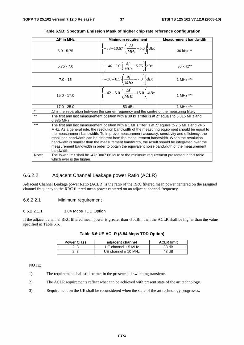
ETSI
ETSI TS 125 102 V7.12.0 (2008-10) 373GPP TS 25.102 version 7.12.0 Release 7
Table 6.5B: Spectrum Emission Mask of higher chip rate reference configuration
Δf* in MHz Minimum requirement Measurement bandwidth
5.0 - 5.75 dBc
MHz
f
⎭⎬⎫
⎩⎨⎧
⎟⎠
⎞⎜⎝
⎛ −Δ⋅−− 0.567.1038
30 kHz **
5.75 - 7.0 dBcMHz
f
⎭⎬⎫
⎩⎨⎧
⎟⎠
⎞⎜⎝
⎛ −Δ⋅−− 75.56.546 30 kHz**
7.0 - 15 dBcMHz
f
⎭⎬⎫
⎩⎨⎧
⎟⎠
⎞⎜⎝
⎛ −Δ⋅−− 0.75.038 1 MHz ***
15.0 - 17.0 dBc
MHz
f
⎭⎬⎫
⎩⎨⎧
⎟⎠
⎞⎜⎝
⎛ −Δ⋅−− 0.150.542
1 MHz ***
17.0 - 25.0 -53 dBc 1 MHz *** * Δf is the separation between the carrier frequency and the centre of the measuring filter. ** The first and last measurement position with a 30 kHz filter is at Δf equals to 5.015 MHz and
6.985 MHz *** The first and last measurement position with a 1 MHz filter is at Δf equals to 7.5 MHz and 24.5
MHz. As a general rule, the resolution bandwidth of the measuring equipment should be equal to the measurement bandwidth. To improve measurement accuracy, sensitivity and efficiency, the resolution bandwidth can be different from the measurement bandwidth. When the resolution bandwidth is smaller than the measurement bandwidth, the result should be integrated over the measurement bandwidth in order to obtain the equivalent noise bandwidth of the measurement bandwidth.
Note: The lower limit shall be -47dBm/7.68 MHz or the minimum requirement presented in this table which ever is the higher.
6.6.2.2 Adjacent Channel Leakage power Ratio (ACLR)
Adjacent Channel Leakage power Ratio (ACLR) is the ratio of the RRC filtered mean power centered on the assigned channel frequency to the RRC filtered mean power centered on an adjacent channel frequency.
6.6.2.2.1 Minimum requirement
6.6.2.2.1.1 3.84 Mcps TDD Option
If the adjacent channel RRC filtered mean power is greater than -50dBm then the ACLR shall be higher than the value specified in Table 6.6.
Table 6.6:UE ACLR (3.84 Mcps TDD Option)
Power Class adjacent channel ACLR limit 2, 3 UE channel ± 5 MHz 33 dB 2, 3 UE channel ± 10 MHz 43 dB
NOTE:
1) The requirement shall still be met in the presence of switching transients.
2) The ACLR requirements reflect what can be achieved with present state of the art technology.
3) Requirement on the UE shall be reconsidered when the state of the art technology progresses.

ETSI
ETSI TS 125 102 V7.12.0 (2008-10) 383GPP TS 25.102 version 7.12.0 Release 7
6.6.2.2.1.2 1.28 Mcps TDD Option
If the adjacent channel RRC filtered mean power is greater than -55dBm then the ACLR shall be higher than the value specified in Table 6.6A.
Table 6.6A: UE ACLR (1.28 Mcps TDD Option)
Power Class adjacent channel ACLR limit 2, 3 UE channel ± 1.6 MHz 33 dB 2, 3 UE channel ± 3.2 MHz 43 dB
NOTE:
1) The requirement shall still be met in the presence of switching transients.
2) The ACLR requirements reflect what can be achieved with present state of the art technology.
3) Requirement on the UE shall be reconsidered when the state of the art technology progresses.
6.6.2.2.1.3 7.68 Mcps TDD Option
If the adjacent channel RRC filtered mean power is greater than -50dBm measured with a 3.84 Mcps RRC filter then the ACLR shall be higher than the value specified in Table 6.6B.
Table 6.6B: UE ACLR of higher chip rate reference configuration
Power Class adjacent channel Chip Rate for RRC Measurement Filter
ACLR limit
2, 3 UE channel ± 7.5 MHz 3.84 MHz 33 dB 2, 3 UE channel ± 12.5 MHz 3.84 MHz 43 dB 2 ,3 UE channel ± 10.0 MHz 7.68 MHz 33 dB 2 ,3 UE channel ± 20.0 MHz 7.68 MHz 43 dB
NOTE:
1) The requirement shall still be met in the presence of switching transients.
2) The ACLR requirements reflect what can be achieved with present state of the art technology.
6.6.3 Spurious emissions
Spurious emissions are emissions which are caused by unwanted transmitter effects such as harmonics emission, parasitic emission, intermodulation products and frequency conversion products, but exclude out of band emissions.
The frequency boundary and the detailed transitions of the limits between the requirement for out band emissions and spectrum emissions are based on ITU-R Recommendations SM.329 [3].
6.6.3.1 Minimum Requirement
6.6.3.1.1 3.84 Mcps TDD Option
These requirements are only applicable for frequencies which are greater than 12.5 MHz away from the UE center carrier frequency.

ETSI
ETSI TS 125 102 V7.12.0 (2008-10) 393GPP TS 25.102 version 7.12.0 Release 7
Table 6.7A: General Spurious emissions requirements (3.84 Mcps TDD Option)
Frequency Bandwidth Measurement Bandwidth Minimum requirement 9 kHz ≤ f < 150 kHz 1 kHz -36 dBm
150 kHz ≤ f < 30 MHz 10 kHz -36 dBm 30 MHz ≤ f < 1000 MHz 100 kHz -36 dBm 1 GHz ≤ f < 12.75 GHz 1 MHz -30 dBm
Table 6.7B: Additional Spurious emissions requirements (3.84 Mcps TDD Option)
Frequency Bandwidth Measurement Bandwidth Minimum requirement 921 MHz ≤ f < 925 MHz 100 kHz -60 dBm (note 1) 925 MHz ≤ f ≤ 935 MHz 100 kHz -67 dBm (note 1) 935 MHz < f ≤ 960 MHz 100 kHz -79 dBm (note 1)
1805 MHz ≤ f ≤ 1880 MHz 100 kHz -71 dBm (note 1) 2620 MHz ≤ f ≤ 2690 MHz 3.84 MHz -37 dBm (note 1)
1884.5 MHz ≤ f ≤ 1919.6 MHz 300 kHz -41 dBm (note 2) NOTE 1: The measurements are made on frequencies which are integer multiples of 200 kHz. As
exceptions, up to five measurements with a level up to the applicable requirements defined in Table 6.7A are permitted for each UARFCN used in the measurement.
NOTE 2: Applicable for transmission in 2010-2025 MHz as defined in subclause 5.2 (a).
6.6.3.1.2 1.28 Mcps TDD Option
These requirements are only applicable for frequencies which are greater than 4 MHz away from the UE center carrier frequency.
Table 6.7C: General Spurious emissions requirements (1.28 Mcps TDD Option)
Frequency Bandwidth Measurement Bandwidth Minimum requirement 9 kHz ≤ f < 150 kHz 1 kHz -36 dBm
150 kHz ≤ f < 30 MHz 10 kHz -36 dBm 30 MHz ≤ f < 1000 MHz 100 kHz -36 dBm 1 GHz ≤ f < 12.75 GHz 1 MHz -30 dBm
Table 6.7D: Additional Spurious emissions requirements (1.28 Mcps TDD Option)
Frequency Bandwidth Measurement Bandwidth Minimum requirement 921 MHz ≤ f < 925 MHz 100 kHz -60 dBm (note) 925 MHz ≤ f ≤ 935 MHz 100 kHz -67 dBm (note) 935 MHz < f ≤ 960 MHz 100 kHz -79 dBm (note)
1805 MHz ≤ f ≤ 1880 MHz 100 kHz -71 dBm (note) 2620 MHz ≤ f ≤ 2690 MHz 3.84 MHz -37 dBm (note)
NOTE: The measurements are made on frequencies which are integer multiples of 200 kHz. As exceptions, up to five measurements with a level up to the applicable requirements defined in Table 6.7C are permitted for each UARFCN used in the measurement.
6.6.3.1.3 7.68 Mcps TDD Option
These requirements are only applicable for frequencies which are greater than 25 MHz away from the UE center carrier frequency.

ETSI
ETSI TS 125 102 V7.12.0 (2008-10) 403GPP TS 25.102 version 7.12.0 Release 7
Table 6.7E: General Spurious emissions requirements (7.68 Mcps TDD Option)
Frequency Bandwidth Measurement Bandwidth Minimum requirement 9 kHz ≤ f < 150 kHz 1 kHz -36 dBm
150 kHz ≤ f < 30 MHz 10 kHz -36 dBm 30 MHz ≤ f < 1000 MHz 100 kHz -36 dBm 1 GHz ≤ f < 12.75 GHz 1 MHz -30 dBm
Table 6.7F: Additional Spurious emissions requirements (7.68 Mcps TDD Option)
Frequency Bandwidth Measurement Bandwidth Minimum requirement 921 MHz ≤ f < 925 MHz 100 kHz -60 dBm (note 1) 925 MHz ≤ f ≤ 935 MHz 100 kHz -67 dBm (note 1) 935 MHz < f ≤ 960 MHz 100 kHz -79 dBm (note 1)
1805 MHz ≤ f ≤ 1880 MHz 100 kHz -71 dBm (note 1) 2620 MHz ≤ f ≤ 2690 MHz 3.84 MHz -37 dBm (note 1)
1884.5 MHz ≤ f ≤ 1919.6 MHz 300 kHz -41 dBm (note 2) NOTE 1: The measurements are made on frequencies which are integer multiples of 200 kHz. As
exceptions, up to five measurements with a level up to the applicable requirements defined in Table 6.7E are permitted for each UARFCN used in the measurement.
NOTE 2: Applicable for transmission in 2010-2025 MHz as defined in subclause 5.2 (a).
6.7 Transmit intermodulation The transmit intermodulation performance is a measure of the capability of the transmitter to inhibit the generation of signals in its non linear elements caused by presence of the wanted signal and an interfering signal reaching the transmitter via the antenna.
6.7.1 Minimum requirement
User Equipment(s) transmitting in close vicinity of each other can produce intermodulation products, which can fall into the UE, or BS receive band as an unwanted interfering signal. The UE intermodulation attenuation is defined by the ratio of the RRC filtered mean power of the wanted signal to the RRC filtered mean power of the intermodulation product when an interfering CW signal is added at a level below the wanted signal.
6.7.1.1 3.84 Mcps TDD Option
The requirement of transmitting intermodulation for carrier spacing 5 MHz is prescribed in Table 6.8.
Table 6.8: Transmit Intermodulation (3.84 Mcps TDD Option)
Interference Signal Frequency Offset 5MHz 10MHz Interference Signal Level -40 dBc Minimum Requirement -31dBc -41dBc
6.7.1.2 1.28 Mcps TDD Option
The requirement of transmitting intermodulation for carrier spacing 1.6 MHz is prescribed in Table 6.8A.
Table 6.8A: Transmit Intermodulation (1.28 Mcps TDD Option)
Interference signal frequency offset 1.6MHz 3.2MHz Interference signal level -40dBc Minimum requirement of intermodulation products -31 dBc -41 dBc

ETSI
ETSI TS 125 102 V7.12.0 (2008-10) 413GPP TS 25.102 version 7.12.0 Release 7
6.7.1.3 7.68 Mcps TDD Option
The requirement of transmitting intermodulation for carrier spacing 10 MHz is prescribed in Table 6.8B.
Table 6.8B: Transmit Intermodulation (7.68 Mcps TDD Option)
Interference Signal Frequency Offset 10MHz 20MHz Interference Signal Level -40 dBc Minimum Requirement -31dBc -41dBc
6.8 Transmit Modulation Transmit modulation defines the modulation quality for expected in-channel RF transmissions from the UE. The requirements apply to all transmissions.
6.8.1 Transmit pulse shape filter
The transmit pulse-shaping filter is a root-raised cosine (RRC) with roll-off α =0.22 in the frequency domain. The impulse response of the chip impulse filter RC0(t) is
( )( ) ( )
⎟⎟
⎠
⎞
⎜⎜
⎝
⎛
⎟⎟⎠
⎞⎜⎜⎝
⎛−
⎟⎟⎠
⎞⎜⎜⎝
⎛++⎟⎟
⎠
⎞⎜⎜⎝
⎛−
=20
41
1cos41sin
CC
CCC
T
t
T
t
T
t
T
t
T
t
tRC
απ
απααπ
Where the roll-off factor α =0.22 and Tc is the chip duration
6.8.2 Error Vector Magnitude
The Error Vector Magnitude is a measure of the difference between the reference waveform and the measured waveform. This difference is called the error vector. Both waveforms pass through a matched Root Raised Cosine filter with bandwidth corresponding to the considered chip rate and roll-off α =0,22. One of the waveforms is then further modified by selecting the frequency, absolute phase, absolute amplitude and chip clock timing so as to minimise the error vector. The EVM result is defined as the square root of the ratio of the mean error vector power to the mean reference power expressed as a %. The period of measurement shall be one transmit timeslot excluding the guard period. See Annex B of TS 34.122 for further details.
6.8.2.1 Minimum Requirement
When 16QAM modulation is not used on any of the uplink code channels, the Error Vector Magnitude shall not exceed 17.5 % for the parameters specified in Table 6.9.
When 16QAM modulation is used on any of the uplink code channels, the modulation accuracy requirement shall not exceed 14% for the parameters specified in Table 6.9
Table 6.9: Test parameters for Error Vector Magnitude/Peak Code Domain Error
Parameter Unit Level UE Output Power dBm ≥-20
Operating conditions Normal conditions Power control step size dB 1
6.8.3 Peak Code Domain Error
This specification is applicable for multi-code transmission only.

ETSI
ETSI TS 125 102 V7.12.0 (2008-10) 423GPP TS 25.102 version 7.12.0 Release 7
The code domain error is computed by projecting the error vector power onto the code domain at a specific spreading factor. The error power for each code is defined as the ratio to the mean power of the reference waveform expressed in dB. The Peak Code Domain Error is defined as the maximum value for Code Domain Error. The period of measurement shall be one transmit timeslot excluding the guard period, and the midamble.
6.8.3.1 Minimum Requirement
The peak code domain error shall not exceed -21 dB at spreading factor 16 for the parameters specified in Table 6.9.
The peak code domain error for 7.68 Mcps option shall not exceed -24 dB at spreading factor 32 for the parameters specified in Table 6.9.
The requirements are defined using the UL reference measurement channel specified in subclause A.2.7.
7 Receiver characteristics
7.1 General Unless detailed the receiver characteristic are specified at the antenna connector of the UE. For UE with an integral antenna only, a reference antenna with a gain of 0 dBi is assumed. UE with an integral antenna may be taken into account by converting these power levels into field strength requirements, assuming a 0 dBi gain antenna. Receiver characteristics for UE(s) with multiple antennas/antenna connectors are FFS.
The UE antenna performance has a significant impact on system performance, and minimum requirements on the antenna efficiency are therefore intended to be included in future versions of this specification. It is recognised that different requirements and test methods are likely to be required for the different types of UE.
All the parameters in Section 7 are defined using the DL reference measurement channel specified in Annex A.2.2 except for UEs capable only of MBSFN reception in which case the DL reference measurement channel specified in Annex A.2.9 is used.
7.2 Diversity characteristics A suitable receiver structure using coherent reception in both channel impulse response estimation, and code tracking procedures is assumed. Three forms of diversity are considered to be available in UTRA/TDD:
Table 7.1: Diversity characteristics for UTRA/TDD
Time diversity Channel coding and interleaving in both up link and down link Multi-path diversity Rake receiver or other suitable receiver structure with maximum combining.
Additional processing elements can increase the delay-spread performance due to increased capture of signal energy.
Antenna diversity Antenna diversity with maximum ratio combing in the base station and optionally in the mobile stations. Possibility for downlink transmit diversity in the base station.
7.3 Reference sensitivity level The reference sensitivity level is the minimum mean power received at the UE antenna port at which the BIT Error Ratio BER shall not exceed a specific value.
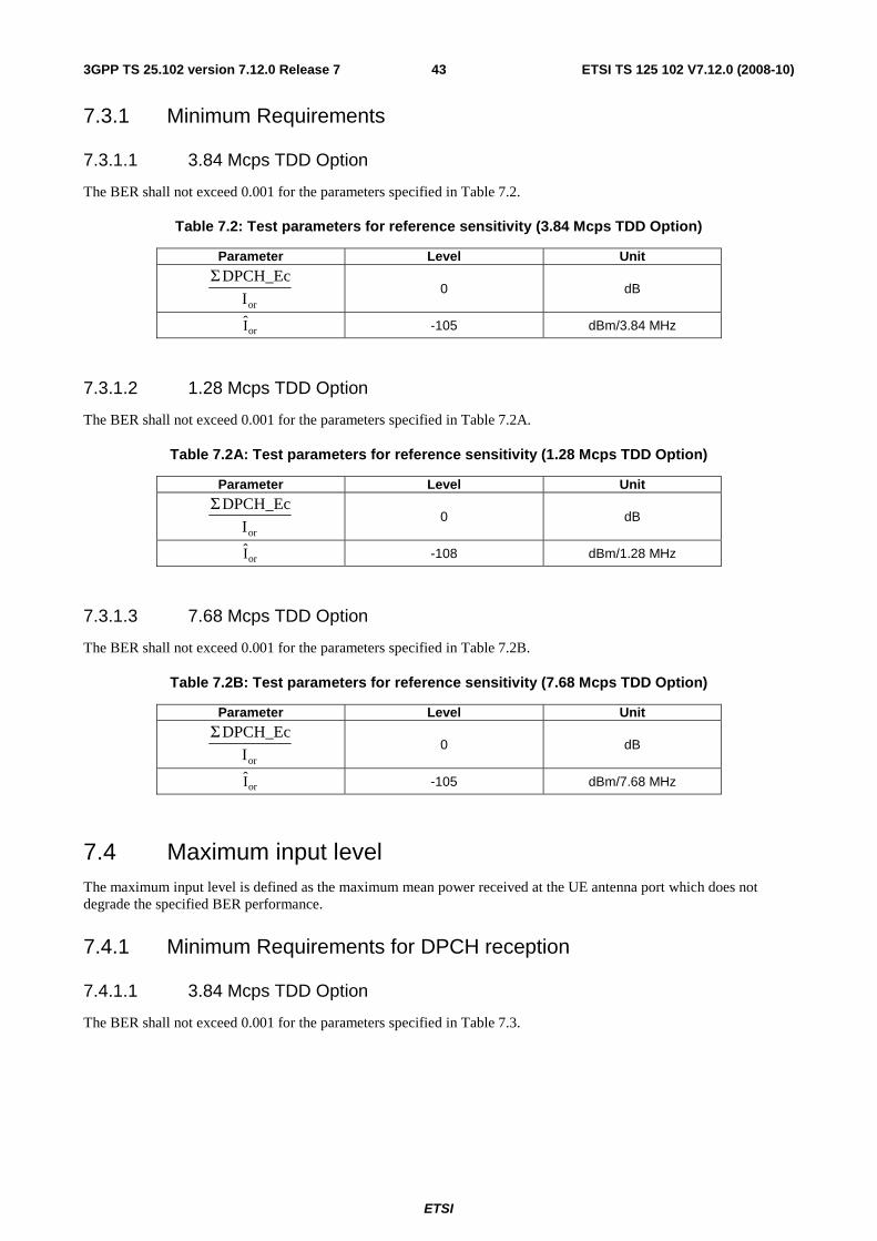
ETSI
ETSI TS 125 102 V7.12.0 (2008-10) 433GPP TS 25.102 version 7.12.0 Release 7
7.3.1 Minimum Requirements
7.3.1.1 3.84 Mcps TDD Option
The BER shall not exceed 0.001 for the parameters specified in Table 7.2.
Table 7.2: Test parameters for reference sensitivity (3.84 Mcps TDD Option)
Parameter Level Unit
orI
DPCH_EcΣ 0 dB
orI -105 dBm/3.84 MHz
7.3.1.2 1.28 Mcps TDD Option
The BER shall not exceed 0.001 for the parameters specified in Table 7.2A.
Table 7.2A: Test parameters for reference sensitivity (1.28 Mcps TDD Option)
Parameter Level Unit
orI
DPCH_EcΣ 0 dB
orI -108 dBm/1.28 MHz
7.3.1.3 7.68 Mcps TDD Option
The BER shall not exceed 0.001 for the parameters specified in Table 7.2B.
Table 7.2B: Test parameters for reference sensitivity (7.68 Mcps TDD Option)
Parameter Level Unit
orI
DPCH_EcΣ 0 dB
orI -105 dBm/7.68 MHz
7.4 Maximum input level The maximum input level is defined as the maximum mean power received at the UE antenna port which does not degrade the specified BER performance.
7.4.1 Minimum Requirements for DPCH reception
7.4.1.1 3.84 Mcps TDD Option
The BER shall not exceed 0.001 for the parameters specified in Table 7.3.
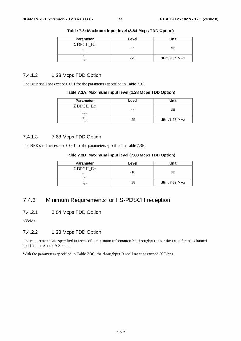
ETSI
ETSI TS 125 102 V7.12.0 (2008-10) 443GPP TS 25.102 version 7.12.0 Release 7
Table 7.3: Maximum input level (3.84 Mcps TDD Option)
Parameter Level Unit
orI
DPCH_EcΣ -7 dB
orI -25 dBm/3.84 MHz
7.4.1.2 1.28 Mcps TDD Option
The BER shall not exceed 0.001 for the parameters specified in Table 7.3A
Table 7.3A: Maximum input level (1.28 Mcps TDD Option)
Parameter Level Unit
orI
DPCH_EcΣ -7 dB
orI -25 dBm/1.28 MHz
7.4.1.3 7.68 Mcps TDD Option
The BER shall not exceed 0.001 for the parameters specified in Table 7.3B.
Table 7.3B: Maximum input level (7.68 Mcps TDD Option)
Parameter Level Unit
orI
DPCH_EcΣ -10 dB
orI -25 dBm/7.68 MHz
7.4.2 Minimum Requirements for HS-PDSCH reception
7.4.2.1 3.84 Mcps TDD Option
<Void>
7.4.2.2 1.28 Mcps TDD Option
The requirements are specified in terms of a minimum information bit throughput R for the DL reference channel specified in Annex A.3.2.2.2.
With the parameters specified in Table 7.3C, the throughput R shall meet or exceed 500kbps.

ETSI
ETSI TS 125 102 V7.12.0 (2008-10) 453GPP TS 25.102 version 7.12.0 Release 7
Table 7.3C
Parameter Level Unit
orI
EcPDSCHHS∑ − _ 0 dB
orI -25 dBm/1.28 MHz
Redundancy and constellation version 6 -
Maximum number of HARQ transmissions 1 -
7.5 Adjacent Channel Selectivity (ACS) Adjacent Channel Selectivity is a measure of a receiver's ability to receive a wanted signal at its assigned channel frequency in the presence of adjacent channel signal at a given frequency offset from the centre frequency of the assigned channel. ACS is the ratio of the receive filter attenuation on the assigned channel frequency to the receiver filter attenuation on the adjacent channel(s).
7.5.1 Minimum Requirement
7.5.1.1 3.84 Mcps TDD Option
The ACS shall be better than the value indicated in Table 7.4 for the test parameters specified in Table 7.5 where the BER shall not exceed 0.001
Table 7.4: Adjacent Channel Selectivity (3.84 Mcps TDD Option)
Power Class Unit ACS 2 dB 33 3 dB 33
Table 7.5: Test parameters for Adjacent Channel Selectivity (3.84 Mcps TDD Option)
Parameter Unit Level
orI
EcDPCH _Σ dB 0
Îor dBm/3.84 MHz -91 Ioac mean power
(modulated) dBm -52
Fuw offset MHz +5 or -5
7.5.1.2 1.28 Mcps TDD Option
The ACS shall be better than the value indicated in table 7.4A for the test parameters specified in table 7.5A where the BER shall not exceed 0.001
Table7.4A: Adjacent Channel Selectivity (1.28 Mcps TDD Option)
Power Class Unit ACS 2 dB 33 3 dB 33
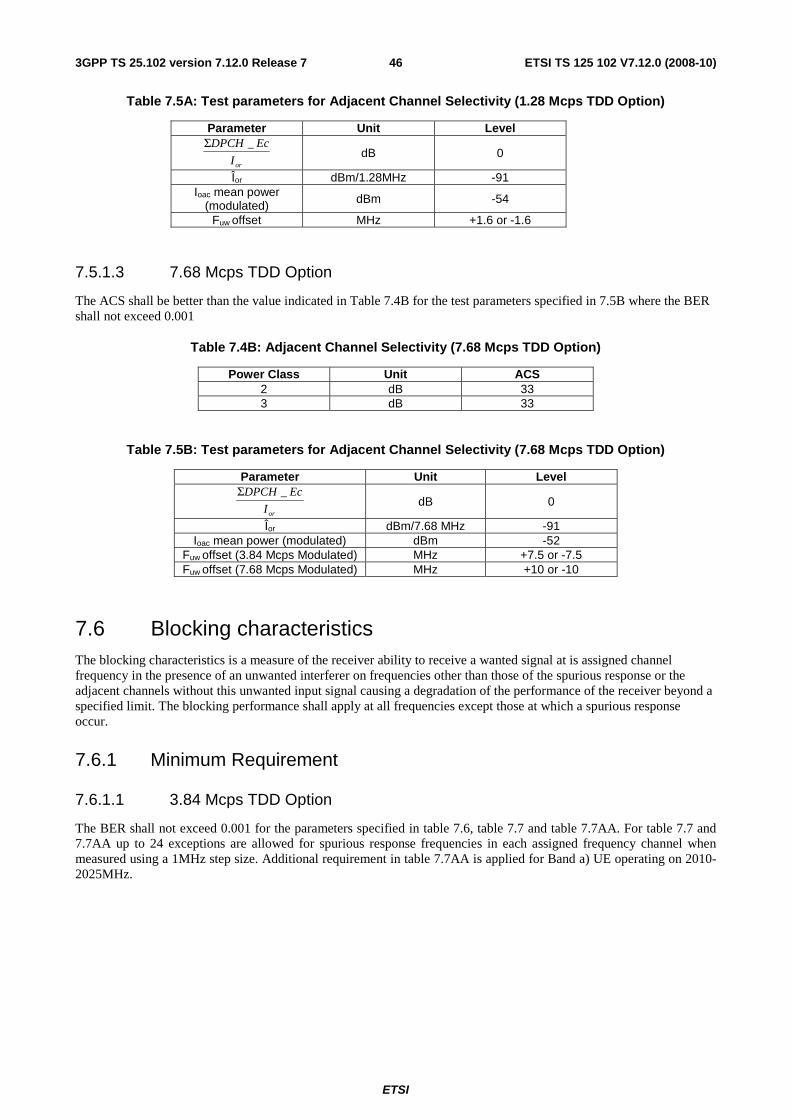
ETSI
ETSI TS 125 102 V7.12.0 (2008-10) 463GPP TS 25.102 version 7.12.0 Release 7
Table 7.5A: Test parameters for Adjacent Channel Selectivity (1.28 Mcps TDD Option)
Parameter Unit Level
orI
EcDPCH _Σ dB 0
Îor dBm/1.28MHz -91 Ioac mean power
(modulated) dBm -54
Fuw offset MHz +1.6 or -1.6
7.5.1.3 7.68 Mcps TDD Option
The ACS shall be better than the value indicated in Table 7.4B for the test parameters specified in 7.5B where the BER shall not exceed 0.001
Table 7.4B: Adjacent Channel Selectivity (7.68 Mcps TDD Option)
Power Class Unit ACS 2 dB 33 3 dB 33
Table 7.5B: Test parameters for Adjacent Channel Selectivity (7.68 Mcps TDD Option)
Parameter Unit Level
orI
EcDPCH _Σ dB 0
Îor dBm/7.68 MHz -91 Ioac mean power (modulated) dBm -52
Fuw offset (3.84 Mcps Modulated) MHz +7.5 or -7.5 Fuw offset (7.68 Mcps Modulated) MHz +10 or -10
7.6 Blocking characteristics The blocking characteristics is a measure of the receiver ability to receive a wanted signal at is assigned channel frequency in the presence of an unwanted interferer on frequencies other than those of the spurious response or the adjacent channels without this unwanted input signal causing a degradation of the performance of the receiver beyond a specified limit. The blocking performance shall apply at all frequencies except those at which a spurious response occur.
7.6.1 Minimum Requirement
7.6.1.1 3.84 Mcps TDD Option
The BER shall not exceed 0.001 for the parameters specified in table 7.6, table 7.7 and table 7.7AA. For table 7.7 and 7.7AA up to 24 exceptions are allowed for spurious response frequencies in each assigned frequency channel when measured using a 1MHz step size. Additional requirement in table 7.7AA is applied for Band a) UE operating on 2010-2025MHz.
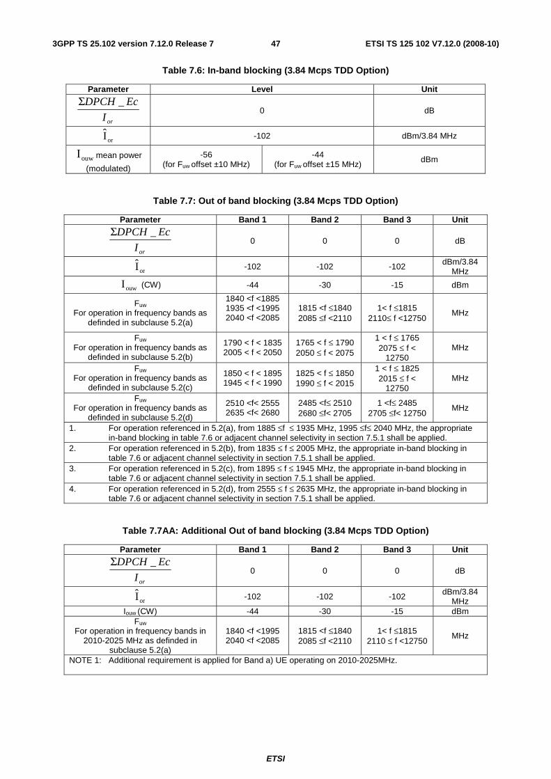
ETSI
ETSI TS 125 102 V7.12.0 (2008-10) 473GPP TS 25.102 version 7.12.0 Release 7
Table 7.6: In-band blocking (3.84 Mcps TDD Option)
Parameter Level Unit
orI
EcDPCH _Σ 0 dB
orI -102 dBm/3.84 MHz
ouwI mean power
(modulated)
-56 (for Fuw offset ±10 MHz)
-44 (for Fuw offset ±15 MHz)
dBm
Table 7.7: Out of band blocking (3.84 Mcps TDD Option)
Parameter Band 1 Band 2 Band 3 Unit
orI
EcDPCH _Σ 0 0 0 dB
orI -102 -102 -102 dBm/3.84 MHz
ouwI (CW) -44 -30 -15 dBm
Fuw
For operation in frequency bands as definded in subclause 5.2(a)
1840 <f <1885 1935 <f <1995 2040 <f <2085
1815 <f ≤1840 2085 ≤f <2110
1< f ≤1815 2110≤ f <12750
MHz
Fuw
For operation in frequency bands as definded in subclause 5.2(b)
1790 < f < 1835 2005 < f < 2050
1765 < f ≤ 1790 2050 ≤ f < 2075
1 < f ≤ 1765 2075 ≤ f <
12750 MHz
Fuw
For operation in frequency bands as definded in subclause 5.2(c)
1850 < f < 1895 1945 < f < 1990
1825 < f ≤ 1850 1990 ≤ f < 2015
1 < f ≤ 1825 2015 ≤ f <
12750 MHz
Fuw
For operation in frequency bands as definded in subclause 5.2(d)
2510 <f< 2555 2635 <f< 2680
2485 <f≤ 2510 2680 ≤f< 2705
1 <f≤ 2485 2705 ≤f< 12750
MHz
1. For operation referenced in 5.2(a), from 1885 ≤f ≤ 1935 MHz, 1995 ≤f≤ 2040 MHz, the appropriate in-band blocking in table 7.6 or adjacent channel selectivity in section 7.5.1 shall be applied.
2. For operation referenced in 5.2(b), from 1835 ≤ f ≤ 2005 MHz, the appropriate in-band blocking in table 7.6 or adjacent channel selectivity in section 7.5.1 shall be applied.
3. For operation referenced in 5.2(c), from 1895 ≤ f ≤ 1945 MHz, the appropriate in-band blocking in table 7.6 or adjacent channel selectivity in section 7.5.1 shall be applied.
4. For operation referenced in 5.2(d), from 2555 ≤ f ≤ 2635 MHz, the appropriate in-band blocking in table 7.6 or adjacent channel selectivity in section 7.5.1 shall be applied.
Table 7.7AA: Additional Out of band blocking (3.84 Mcps TDD Option)
Parameter Band 1 Band 2 Band 3 Unit
orI
EcDPCH _Σ 0 0 0 dB
orI -102 -102 -102 dBm/3.84 MHz
Iouw (CW) -44 -30 -15 dBm Fuw
For operation in frequency bands in 2010-2025 MHz as definded in
subclause 5.2(a)
1840 <f <1995 2040 <f <2085
1815 <f ≤1840 2085 ≤f <2110
1< f ≤1815 2110 ≤ f <12750
MHz
NOTE 1: Additional requirement is applied for Band a) UE operating on 2010-2025MHz.

ETSI
ETSI TS 125 102 V7.12.0 (2008-10) 483GPP TS 25.102 version 7.12.0 Release 7
7.6.1.2 1.28 Mcps TDD Option
The BER shall not exceed 0.001 for the parameters specified in table 7.6A and table 7.7A. For table 7.7A up to 24 exceptions are allowed for spurious response frequencies in each assigned frequency channel when measured using a 1MHz step size.
Table 7.6A: In-band blocking (1.28 Mcps TDD Option)
Parameter Level Unit
orI
EcDPCH _Σ 0 dB
orI -105 dBm/1.28 MHz
ouwI mean power (modulated) -61 (for Fuw offset ±3.2 MHz)
-49 (for Fuw offset ±4.8 MHz) dBm
Table 7.7A: Out of band blocking (1.28 Mcps TDD Option)
Parameter Band 1 Band 2 Band 3 Unit
orI
EcDPCH _Σ 0 0 0 dB
orI -105 -105 -105 dBm/1.28 MHz
ouwI (CW) -44 -30 -15 dBm
Fuw
For operation in frequency bands as definded in subclause 5.2(a)
1840 <f <1895.2 1924.8 <f <2005.2 2029.8 <f <2085
1815 <f ≤1840 2085 ≤f <2110
1< f ≤1815 2110 ≤ f <12750
MHz
Fuw
For operation in frequency bands as definded in subclause 5.2(b)
1790 < f < 1845.2 1914.8 < f <
1925.2 1994.8 < f < 2050
1765 < f ≤ 1790 2050 ≤ f < 2075
1 < f ≤ 1765 2075 ≤ f < 12750
MHz
Fuw
For operation in frequency bands as definded in subclause 5.2(c)
1850 < f < 1905.2 1934.8 < f < 1990
1825 < f ≤ 1850 1990 ≤ f < 2015
1 < f ≤ 1825 2015 ≤ f < 12750
MHz
Fuw
For operation in frequency bands as definded in subclause 5.2(d)
2510 < f < 2565.2 2624.8 < f < 2680
2485 < f ≤ 2510 2680 ≤ f < 2705
1< f ≤ 2485 2705 ≤ f < 12750
MHz
1. For operation referenced in 5.2(a), from 1895.2 ≤f ≤ 1924.8 MHz, 2005.2 ≤f≤ 2029.8 MHz, the appropriate in-band blocking in table 7.6A or adjacent channel selectivity in section 7.5.1.2shall be applied.
2. For operation referenced in 5.2(b), from 1845.2 ≤ f < 1914.8 MHz, and 1925.2< f < 1994.8 MHz, the appropriate in-band blocking in table 7.6A or adjacent channel selectivity in section 7.5.1.2 shall be applied.
3. For operation referenced in 5.2(c), from 1905.2 ≤ f ≤ 1934.8 MHz, the appropriate in-band blocking in table 7.6A or adjacent channel selectivity in section 7.5.1.2 shall be applied.
4. For operation referenced in 5.2(d), from 2565.2 ≤ f ≤ 2624.8 MHz, the appropriate in-band blocking in table 7.6 or adjacent channel selectivity in section 7.5.1 shall be applied.
7.6.1.3 7.68 Mcps TDD Option
The BER shall not exceed 0.001 for the parameters specified in table 7.6B, 7.7B and table 7.7CC. For table 7.7B and 7.7CC up to 24 exceptions are allowed for spurious response frequencies in each assigned frequency channel when measured using a 1MHz step size. Additional requirement in table 7.7CC is applied for Band a) UE operating on 2010-2025MHz.

ETSI
ETSI TS 125 102 V7.12.0 (2008-10) 493GPP TS 25.102 version 7.12.0 Release 7
Table 7.6B: In-band blocking
Parameter Level Unit
orI
EcDPCH _Σ 0 dB
orI -102 dBm/7.68 MHz
ouwI mean power
(modulated)
-53 (for Fuw offset ±20 MHz)
-41 (for Fuw offset ±30 MHz)
dBm
Table 7.7B: Out of band blocking
Parameter Band 1 Band 2 Band 3 Unit
orI
EcDPCH _Σ 0 0 0 dB
orI -102 -102 -102 dBm/7.68 MHz
ouwI (CW) -44 -30 -15 dBm
Fuw
For operation in frequency bands as definded in subclause 5.2(a)
1840 <f <1870 1950 <f <1980 2055 <f <2085
1815 <f ≤1840 2085 ≤f <2110
1< f ≤1815 2110≤ f <12750
MHz
Fuw
For operation in frequency bands as definded in subclause 5.2(b)
1790 < f < 1820 2020 < f < 2050
1765 < f ≤ 1790 2050 ≤ f < 2075
1 < f ≤ 1765 2075 ≤ f <
12750 MHz
Fuw
For operation in frequency bands as definded in subclause 5.2(c)
1850 < f < 1880 1960 < f < 1990
1825 < f ≤ 1850 1990 ≤ f < 2015
1 < f ≤ 1825 2015 ≤ f <
12750 MHz
Fuw
For operation in frequency bands as definded in subclause 5.2(d)
2510 <f< 2540 2650 <f< 2680
2485 <f≤ 2510 2680 ≤f< 2705
1 <f≤ 2485 2705 ≤f< 12750
MHz
1. For operation referenced in 5.2(a), from 1870 ≤f ≤ 1950 MHz, 1980 ≤f ≤ 2055 MHz, the appropriate in-band blocking in table 7.6B or adjacent channel selectivity in section 7.5.1.3 shall be applied.
2. For operation referenced in 5.2(b), from 1820 ≤ f ≤ 2020 MHz, the appropriate in-band blocking in table 7.6B or adjacent channel selectivity in section 7.5.1.3 shall be applied.
3. For operation referenced in 5.2(c), from 1880 ≤ f ≤ 1960 MHz, the appropriate in-band blocking in table 7.6B or adjacent channel selectivity in section 7.5.1.3 shall be applied.
4. For operation referenced in 5.2(d), from 2540 ≤ f ≤ 2650 MHz, the appropriate in-band blocking in table 7.6B or adjacent channel selectivity in section 7.5.1.3 shall be applied.
Table 7.7CC: Additional Out of band blocking (7.68 Mcps TDD Option)
Parameter Band 1 Band 2 Band 3 Unit
orI
EcDPCH _Σ 0 0 0 dB
orI -102 -102 -102 dBm/3.84 MHz
Iouw (CW) -44 -30 -15 dBm Fuw
For operation in frequency bands in 2010-2025 MHz as definded in
subclause 5.2(a)
1840 <f <1995 2040 <f <2085
1815 <f ≤1840 2085 ≤f <2110
1< f ≤1815 2110 ≤ f <12750
MHz
NOTE 1: Additional requirement is applied for Band a) UE operating on 2010-2025MHz.

ETSI
ETSI TS 125 102 V7.12.0 (2008-10) 503GPP TS 25.102 version 7.12.0 Release 7
7.7 Spurious response Spurious response is a measure of the receiver's ability to receive a wanted signal on its assigned channel frequency without exceeding a given degradation due to the presence of an unwanted CW interfering signal at any other frequency at which a response is obtained i.e. for which the blocking limit is not met.
7.7.1 Minimum Requirement
7.7.1.1 3.84 Mcps TDD Option
The BER shall not exceed 0.001 for the parameters specified in Table 7.8.
Table 7.8: Spurious Response (3.84 Mcps TDD Option)
Parameter Level Unit
orI
EcDPCH _Σ 0 dB
orI -102 dBm/3.84 MHz
ouwI (CW) -44 dBm
Fuw Spurious response frequencies
MHz
7.7.1.2 1.28 Mcps TDD Option
The BER shall not exceed 0.001 for the parameters specified in Table 7.8A.
Table 7.8A: Spurious Response (1.28 Mcps TDD Option)
Parameter Level Unit
orI
EcDPCH _Σ 0 dB
orI -105 dBm/1.28 MHz
ouwI (CW) -44 dBm
Fuw Spurious response frequencies MHz
7.7.1.3 7.68 Mcps TDD Option
The BER shall not exceed 0.001 for the parameters specified in Table 7.8B.
Table 7.8B: Spurious Response
Parameter Level Unit
orI
EcDPCH _Σ 0 dB
orI -102 dBm/7.68 MHz
ouwI (CW) -44 dBm
Fuw Spurious response frequencies MHz
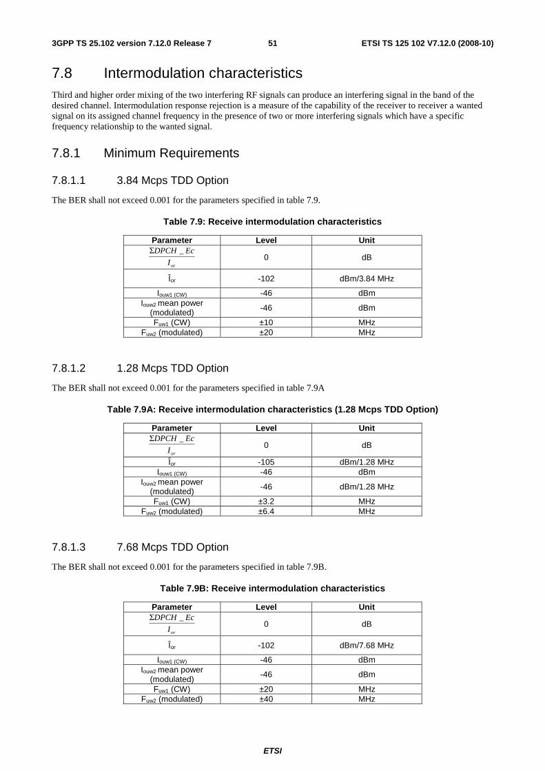
ETSI
ETSI TS 125 102 V7.12.0 (2008-10) 513GPP TS 25.102 version 7.12.0 Release 7
7.8 Intermodulation characteristics Third and higher order mixing of the two interfering RF signals can produce an interfering signal in the band of the desired channel. Intermodulation response rejection is a measure of the capability of the receiver to receiver a wanted signal on its assigned channel frequency in the presence of two or more interfering signals which have a specific frequency relationship to the wanted signal.
7.8.1 Minimum Requirements
7.8.1.1 3.84 Mcps TDD Option
The BER shall not exceed 0.001 for the parameters specified in table 7.9.
Table 7.9: Receive intermodulation characteristics
Parameter Level Unit
orI
EcDPCH _Σ 0 dB
Îor -102 dBm/3.84 MHz
Iouw1 (CW) -46 dBm Iouw2 mean power
(modulated) -46 dBm
Fuw1 (CW) ±10 MHz Fuw2 (modulated) ±20 MHz
7.8.1.2 1.28 Mcps TDD Option
The BER shall not exceed 0.001 for the parameters specified in table 7.9A
Table 7.9A: Receive intermodulation characteristics (1.28 Mcps TDD Option)
Parameter Level Unit
orI
EcDPCH _Σ
0 dB
Îor -105 dBm/1.28 MHz Iouw1 (CW) -46 dBm
Iouw2 mean power (modulated) -46 dBm/1.28 MHz
Fuw1 (CW) ±3.2 MHz Fuw2 (modulated) ±6.4 MHz
7.8.1.3 7.68 Mcps TDD Option
The BER shall not exceed 0.001 for the parameters specified in table 7.9B.
Table 7.9B: Receive intermodulation characteristics
Parameter Level Unit
orI
EcDPCH _Σ 0 dB
Îor -102 dBm/7.68 MHz
Iouw1 (CW) -46 dBm Iouw2 mean power
(modulated) -46 dBm
Fuw1 (CW) ±20 MHz Fuw2 (modulated) ±40 MHz

ETSI
ETSI TS 125 102 V7.12.0 (2008-10) 523GPP TS 25.102 version 7.12.0 Release 7
7.9 Spurious emissions The Spurious Emissions Power is the power of emissions generated or amplified in a receiver that appear at the UE antenna connector.
7.9.1 Minimum Requirement
7.9.1.1 3.84 Mcps TDD Option
The power of any spurious emission shall not exceed:
Table 7.10: Receiver spurious emission requirements (3.84 Mcps TDD Option)
Band Maximum level
Measurement Bandwidth
Note
30 MHz - 1 GHz -57 dBm 100 kHz 1 GHz - 1.9 GHz and
1.92 GHz - 2.01 GHz and 2.025 GHz - 2.11 GHz and
2.17 GHz - 2.57 GHz
-47 dBm 1 MHz
1.9 GHz - 1.92 GHz and 2.01 GHz - 2.025 GHz and 2.11 GHz - 2.170 GHz and
2.57 GHz - 2.69 GHz
-60 dBm 3.84 MHz
2.69 GHz - 12.75 GHz -47 dBm 1 MHz
7.9.1.2 1.28 Mcps TDD Option
The power of any spurious emission shall not exceed:
Table 7.10A: Receiver spurious emission requirements (1.28 Mcps TDD Option)
Band Maximum level
Measurement Bandwidth
Note
30 MHz - 1 GHz -57 dBm 100 kHz 1 GHz - 1.9 GHz and
1.92 GHz - 2.01 GHz and 2.025 GHz - 2.11 GHz and
2.17GHz - 2.57GHz
-47 dBm 1 MHz
1.9 GHz - 1.92 GHz and 2.01 GHz - 2.025 GHz and 2.11 GHz - 2.170 GHz and
2.57GHz - 2.69GHz
-64 dBm 1.28 MHz
2.69 GHz - 12.75 GHz -47 dBm 1 MHz
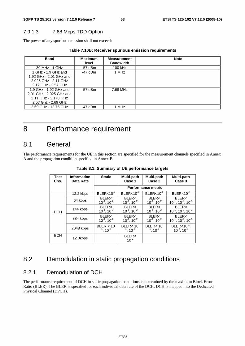
ETSI
ETSI TS 125 102 V7.12.0 (2008-10) 533GPP TS 25.102 version 7.12.0 Release 7
7.9.1.3 7.68 Mcps TDD Option
The power of any spurious emission shall not exceed:
Table 7.10B: Receiver spurious emission requirements
Band Maximum level
Measurement Bandwidth
Note
30 MHz - 1 GHz -57 dBm 100 kHz 1 GHz - 1.9 GHz and
1.92 GHz - 2.01 GHz and 2.025 GHz - 2.11 GHz 2.17 GHz - 2.57 GHz
-47 dBm 1 MHz
1.9 GHz - 1.92 GHz and 2.01 GHz - 2.025 GHz and
2.11 GHz - 2.170 GHz 2.57 Ghz - 2.69 GHz
-57 dBm 7.68 MHz
2.69 GHz - 12.75 GHz -47 dBm 1 MHz
8 Performance requirement
8.1 General The performance requirements for the UE in this section are specified for the measurement channels specified in Annex A and the propagation condition specified in Annex B.
Table 8.1: Summary of UE performance targets
Static Multi-path Case 1
Multi-path Case 2
Multi-path Case 3
Test Chs.
Information Data Rate
Performance metric
12.2 kbps BLER<10-2 BLER<10-2 BLER<10-2 BLER<10-2
64 kbps BLER< 10-1, 10-2
BLER< 10-1, 10-2
BLER< 10-1, 10-2
BLER< 10-1, 10-2, 10-3
144 kbps BLER< 10-1, 10-2
BLER< 10-1, 10-2
BLER< 10-1, 10-2
BLER< 10-1, 10-2, 10-3
384 kbps BLER< 10-1, 10-2
BLER< 10-1, 10-2
BLER< 10-1, 10-2
BLER< 10-1, 10-2, 10-3
DCH
2048 kbps BLER < 10-
1, 10-2 BLER< 10-
1, 10-2 BLER< 10-
1, 10-2 BLER<10-1,
10-2, 10-3 BCH
12.3kbps BLER< 10-2
8.2 Demodulation in static propagation conditions
8.2.1 Demodulation of DCH
The performance requirement of DCH in static propagation conditions is determined by the maximum Block Error Ratio (BLER). The BLER is specified for each individual data rate of the DCH. DCH is mapped into the Dedicated Physical Channel (DPCH).

ETSI
ETSI TS 125 102 V7.12.0 (2008-10) 543GPP TS 25.102 version 7.12.0 Release 7
8.2.1.1 Minimum requirement
8.2.1.1.1 3.84 Mcps TDD Option
For the parameters specified in Table 8.2 the BLER should not exceed the piece-wise linear BLER curve specified in Table 8.3. These requirements are applicable for TFCS size 16.
Table 8.2: DCH parameters in static propagation conditions (3.84 Mcps TDD Option)
Parameters Unit Test 1 Test 2 Test 3 Test 4 Test 5
or
c
I
EDPCH _Σ
dB -6 -3 0 0 0
Ioc dBm/3.84 MHz -60 Cell Parameter* 0,1 -
DPCH Channelization
Codes*
C(k,Q) C(i,16) i=1,2
C(i,16) i=1 . .5
C(i,16) i=1 . .9
C(i,16) i=1 . .8
-
OCNS Channelization
Code*
C(k,Q) C(3,16) C(6,16) - - -
Information Data Rate
kbps 12.2 64 144 384 2048
*Note: Refer to TS 25.223 for definition of channelization codes and cell parameter.
Table 8.3: Performance requirements in AWGN channel (3.84 Mcps TDD Option)
Test Number
oc
or
I
I[dB]
BLER
1 1.1 10-2 3.5 10-1 2 3.8 10-2 3.4 10-1 3 3.6 10-2 2.7 10-1 4 3.0 10-2 3.5 10-1 5 3.6 10-2
8.2.1.1.2 1.28 Mcps TDD Option
For the parameters specified in Table 8.2A the BLER should not exceed the piece-wise linear BLER curve specified in Table 8.3A.
Table 8.2A: DCH parameters in static propagation conditions (1.28 Mcps TDD Option)
Parameters Unit Test 1 Test 2 Test 3 Test 4 Number of DPCHo 8 2 2 0
Scrambling code and basic midamble code
number*
0 0 0 0
DPCH Channelization Codes*
C(k,Q) C(i,16) i=1,2
C(i,16) i=1…8
C(i,16) i=1…8
C(i,16) i=1…10
DPCHo Channelization Codes*
C(k,Q) C(i,16) 3≤ i ≤10
C(i,16) 9≤ i ≤10
C(i,16) 9≤ i ≤10
-
or
co
I
EDPCH _
dB -10 -10 -10 0
Ioc DBm/1.28MHz -60 Information Data Rate Kbps 12.2 64 144 384 *Note: Refer to TS 25.223 for definition of channelization codes, scrambling code and basic midamble code.
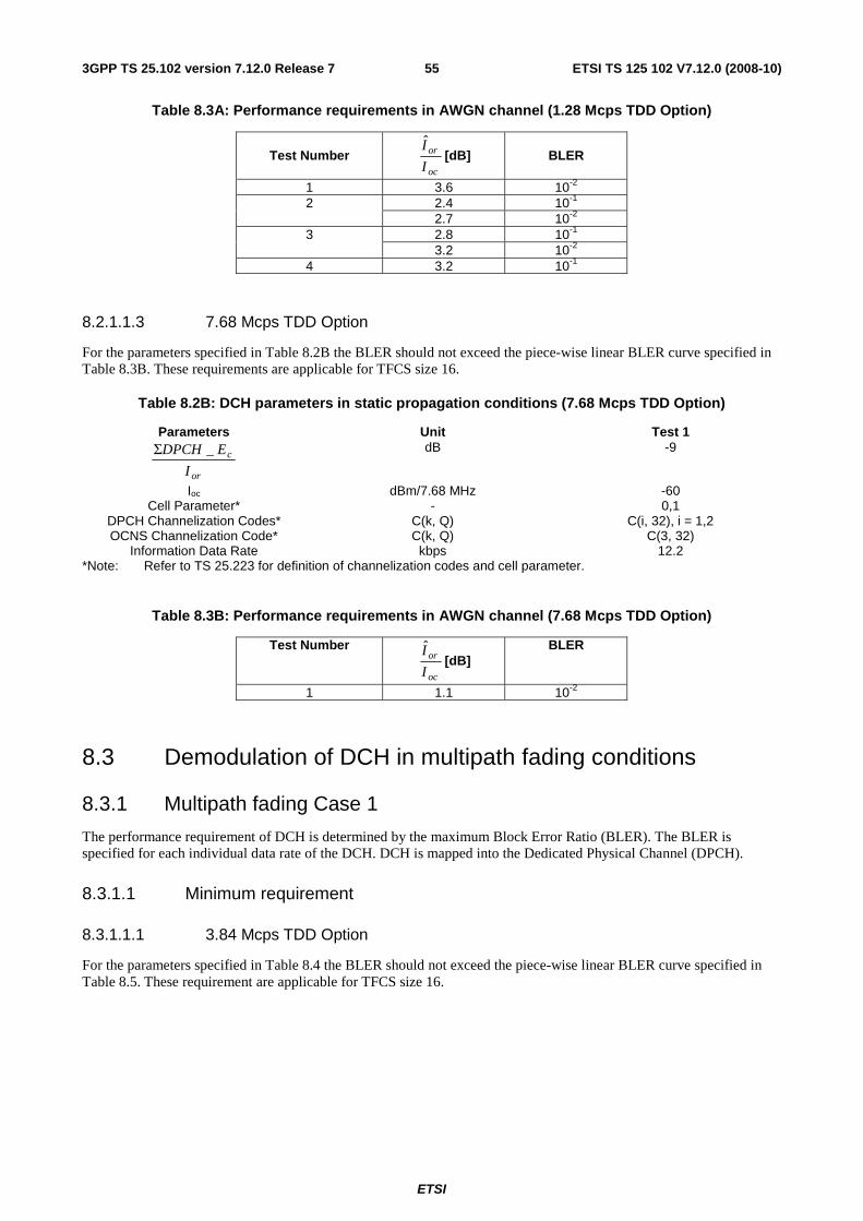
ETSI
ETSI TS 125 102 V7.12.0 (2008-10) 553GPP TS 25.102 version 7.12.0 Release 7
Table 8.3A: Performance requirements in AWGN channel (1.28 Mcps TDD Option)
Test Number oc
or
I
I[dB] BLER
1 3.6 10-2 2.4 10-1 2 2.7 10-2 2.8 10-1 3 3.2 10-2
4 3.2 10-1
8.2.1.1.3 7.68 Mcps TDD Option
For the parameters specified in Table 8.2B the BLER should not exceed the piece-wise linear BLER curve specified in Table 8.3B. These requirements are applicable for TFCS size 16.
Table 8.2B: DCH parameters in static propagation conditions (7.68 Mcps TDD Option)
Parameters Unit Test 1
or
c
I
EDPCH _Σ
dB -9
Ioc dBm/7.68 MHz -60 Cell Parameter* - 0,1
DPCH Channelization Codes* C(k, Q) C(i, 32), i = 1,2 OCNS Channelization Code* C(k, Q) C(3, 32)
Information Data Rate kbps 12.2 *Note: Refer to TS 25.223 for definition of channelization codes and cell parameter.
Table 8.3B: Performance requirements in AWGN channel (7.68 Mcps TDD Option)
Test Number
oc
or
I
I[dB]
BLER
1 1.1 10-2
8.3 Demodulation of DCH in multipath fading conditions
8.3.1 Multipath fading Case 1
The performance requirement of DCH is determined by the maximum Block Error Ratio (BLER). The BLER is specified for each individual data rate of the DCH. DCH is mapped into the Dedicated Physical Channel (DPCH).
8.3.1.1 Minimum requirement
8.3.1.1.1 3.84 Mcps TDD Option
For the parameters specified in Table 8.4 the BLER should not exceed the piece-wise linear BLER curve specified in Table 8.5. These requirement are applicable for TFCS size 16.

ETSI
ETSI TS 125 102 V7.12.0 (2008-10) 563GPP TS 25.102 version 7.12.0 Release 7
Table 8.4: DCH parameters in multipath Case 1 channel (3.84 Mcps TDD Option)
Parameters Unit Test 1 Test 2 Test 3 Test 4 Test 5
or
c
I
EDPCH _Σ
DB -6 -3 0 0 0
Ioc dBm/3.84 MHz -60 Cell Parameter* 0,1 -
DPCH Channelization
Codes*
C(k,Q) C(i,16) i=1,2
C(i,16) i=1 . .5
C(i,16) i=1 . .9
C(i,16) i=1 . .8
-
OCNS Channelization
Code*
C(k,Q) C(3,16) C(6,16) - - -
Information Data Rate
kbps 12.2 64 144 384 2048
*Note: Refer to TS 25.223 for definition of channelization codes and cell parameter.
Table 8.5: Performance requirements in multipath Case 1 channel (3.84 Mcps TDD Option)
Test Number oc
or
I
I[dB] BLER
1 13.9 10-2 13.7 10-1 2 19.8 10-2 14.1 10-1 3 20.6 10-2 13.8 10-1 4 20.0 10-2 13.2 10-1 5 17.8 10-2
8.3.1.1.2 1.28 Mcps TDD Option
For the parameters specified in Table 8.4A the BLER should not exceed the piece-wise linear BLER curve specified in Table 8.5A.
Table 8.4A: DCH parameters in multipath Case 1 channel (1.28 Mcps TDD Option)
Parameters Unit Test 1 Test 2 Test 3 Test 4 Number of DPCHo 8 2 2 0
Scrambling code and basic midamble code
number*
0 0 0 0
DPCH Channelization Codes*
C(k,Q) C(i,16) i=1,2
C(i,16) i=1…8
C(i,16) i=1…8
C(i,16) i=1…10
DPCHo Channelization Codes*
C(k,Q) C(i,16) 3≤ i ≤10
C(i,16) 9≤ i ≤10
C(i,16) 9≤ i ≤10
-
or
co
I
EDPCH _
DB -10 -10 -10 0
Ioc dBm/1.28MHz -60 Information Data Rate Kbps 12.2 64 144 384 *Note: Refer to TS 25.223 for definition of channelization codes, scrambling code and basic midamble code.
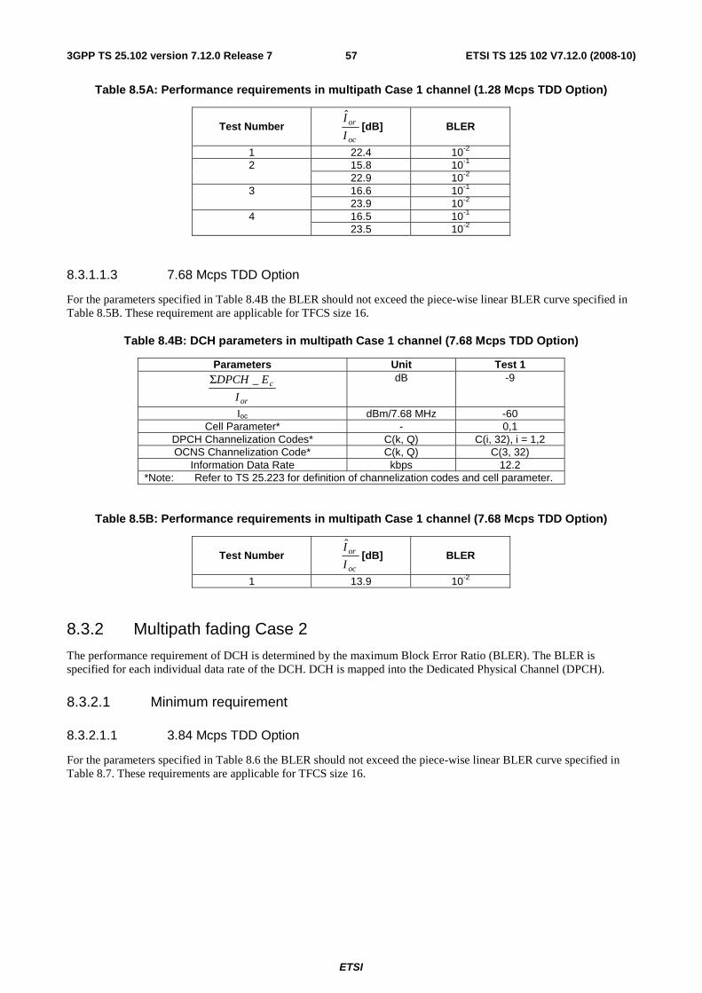
ETSI
ETSI TS 125 102 V7.12.0 (2008-10) 573GPP TS 25.102 version 7.12.0 Release 7
Table 8.5A: Performance requirements in multipath Case 1 channel (1.28 Mcps TDD Option)
Test Number oc
or
I
I[dB] BLER
1 22.4 10-2 15.8 10-1 2 22.9 10-2 16.6 10-1 3 23.9 10-2 16.5 10-1 4 23.5 10-2
8.3.1.1.3 7.68 Mcps TDD Option
For the parameters specified in Table 8.4B the BLER should not exceed the piece-wise linear BLER curve specified in Table 8.5B. These requirement are applicable for TFCS size 16.
Table 8.4B: DCH parameters in multipath Case 1 channel (7.68 Mcps TDD Option)
Parameters Unit Test 1
or
c
I
EDPCH _Σ
dB -9
Ioc dBm/7.68 MHz -60 Cell Parameter* - 0,1
DPCH Channelization Codes* C(k, Q) C(i, 32), i = 1,2 OCNS Channelization Code* C(k, Q) C(3, 32)
Information Data Rate kbps 12.2 *Note: Refer to TS 25.223 for definition of channelization codes and cell parameter.
Table 8.5B: Performance requirements in multipath Case 1 channel (7.68 Mcps TDD Option)
Test Number oc
or
I
I[dB] BLER
1 13.9 10-2
8.3.2 Multipath fading Case 2
The performance requirement of DCH is determined by the maximum Block Error Ratio (BLER). The BLER is specified for each individual data rate of the DCH. DCH is mapped into the Dedicated Physical Channel (DPCH).
8.3.2.1 Minimum requirement
8.3.2.1.1 3.84 Mcps TDD Option
For the parameters specified in Table 8.6 the BLER should not exceed the piece-wise linear BLER curve specified in Table 8.7. These requirements are applicable for TFCS size 16.
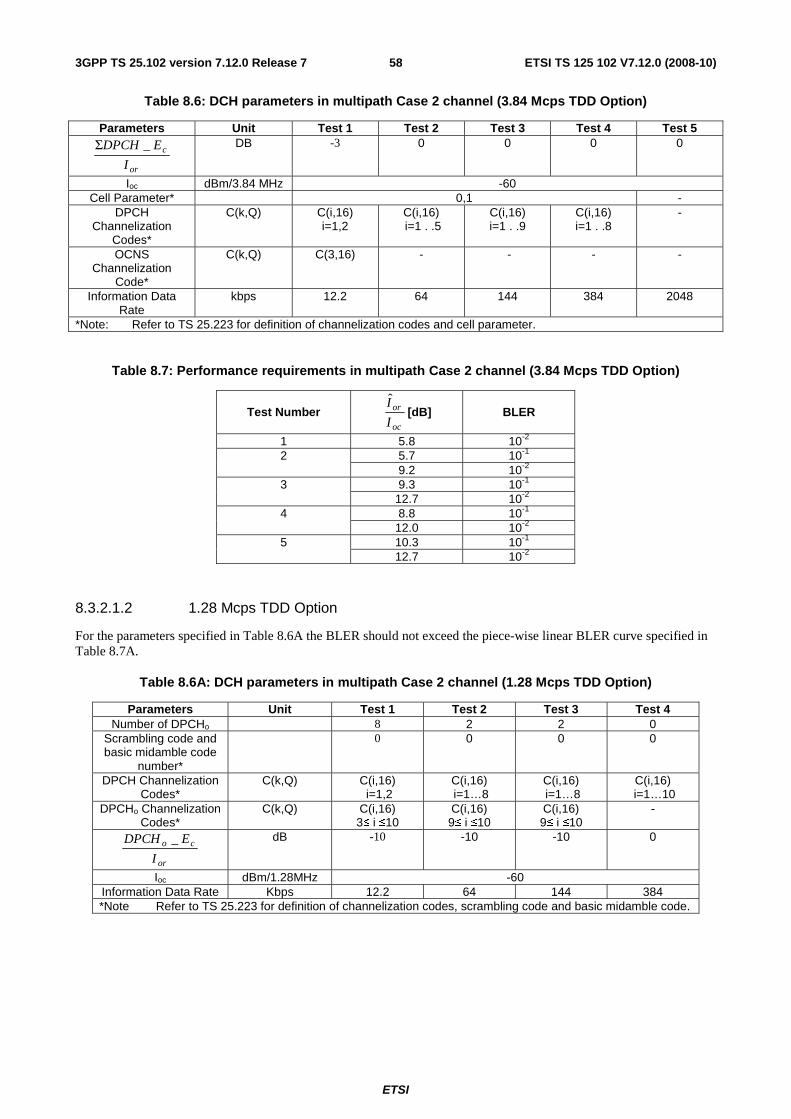
ETSI
ETSI TS 125 102 V7.12.0 (2008-10) 583GPP TS 25.102 version 7.12.0 Release 7
Table 8.6: DCH parameters in multipath Case 2 channel (3.84 Mcps TDD Option)
Parameters Unit Test 1 Test 2 Test 3 Test 4 Test 5
or
c
I
EDPCH _Σ
DB -3 0 0 0 0
Ioc dBm/3.84 MHz -60 Cell Parameter* 0,1 -
DPCH Channelization
Codes*
C(k,Q) C(i,16) i=1,2
C(i,16) i=1 . .5
C(i,16) i=1 . .9
C(i,16) i=1 . .8
-
OCNS Channelization
Code*
C(k,Q) C(3,16) - - - -
Information Data Rate
kbps 12.2 64 144 384 2048
*Note: Refer to TS 25.223 for definition of channelization codes and cell parameter.
Table 8.7: Performance requirements in multipath Case 2 channel (3.84 Mcps TDD Option)
Test Number oc
or
I
I[dB] BLER
1 5.8 10-2 5.7 10-1 2 9.2 10-2 9.3 10-1 3
12.7 10-2 8.8 10-1 4
12.0 10-2 10.3 10-1 5 12.7 10-2
8.3.2.1.2 1.28 Mcps TDD Option
For the parameters specified in Table 8.6A the BLER should not exceed the piece-wise linear BLER curve specified in Table 8.7A.
Table 8.6A: DCH parameters in multipath Case 2 channel (1.28 Mcps TDD Option)
Parameters Unit Test 1 Test 2 Test 3 Test 4 Number of DPCHo 8 2 2 0
Scrambling code and basic midamble code
number*
0 0 0 0
DPCH Channelization Codes*
C(k,Q) C(i,16) i=1,2
C(i,16) i=1…8
C(i,16) i=1…8
C(i,16) i=1…10
DPCHo Channelization Codes*
C(k,Q) C(i,16) 3≤ i ≤10
C(i,16) 9≤ i ≤10
C(i,16) 9≤ i ≤10
-
or
co
I
EDPCH _
dB -10 -10 -10 0
Ioc dBm/1.28MHz -60 Information Data Rate Kbps 12.2 64 144 384 *Note Refer to TS 25.223 for definition of channelization codes, scrambling code and basic midamble code.

ETSI
ETSI TS 125 102 V7.12.0 (2008-10) 593GPP TS 25.102 version 7.12.0 Release 7
Table 8.7A: Performance requirements in multipath Case 2 channel (1.28 Mcps TDD Option)
Test Number oc
or
I
I[dB] BLER
1 13.6 10-2 9.8 10-1 2
13.9 10-2 10.3 10-1 3 14.4 10-2 10.5 10-1 4 14.4 10-2
8.3.2.1.3 7.68 Mcps TDD Option
For the parameters specified in Table 8.6B the BLER should not exceed the piece-wise linear BLER curve specified in Table 8.7B. These requirements are applicable for TFCS size 16.
Table 8.6B: DCH parameters in multipath Case 2 channel (7.68 Mcps TDD Option)
Parameters Unit Test 1
or
c
I
EDPCH _Σ
dB -6
Ioc dBm/7.68 MHz -60 Cell Parameter (note) - 0,1
DPCH Channelization Codes (note) C(k, Q) C(i, 32), i = 1,2 OCNS Channelization Code (note) C(k, Q) C(3, 32)
Information Data Rate kbps 12.2 NOTE: Refer to TS 25.223 for definition of channelization codes and cell parameter.
Table 8.7B: Performance requirements in multipath Case 2 channel (7.68 Mcps TDD Option)
Test Number oc
or
I
I[dB] BLER
1 5.8 10-2
8.3.3 Multipath fading Case 3
The performance requirement of DCH is determined by the maximum Block Error Ratio (BLER). The BLER is specified for each individual data rate of the DCH. DCH is mapped into the Dedicated Physical Channel (DPCH).

ETSI
ETSI TS 125 102 V7.12.0 (2008-10) 603GPP TS 25.102 version 7.12.0 Release 7
8.3.3.1 Minimum requirement
8.3.3.1.1 3.84 Mcps TDD Option
For the parameters specified in Table 8.8 the BLER should not exceed the piece-wise linear BLER curve specified in Table 8.9. These requirements are applicable for TFCS size 16.
Table 8.8: DCH parameters in multipath Case 3 channel (3.84 Mcps TDD Option)
Parameters Unit Test 1 Test 2 Test 3 Test 4 Test 5
or
c
I
EDPCH _Σ
dB -3 0 0 0 0
Ioc dBm/3.84 MHz -60 Cell Parameter* 0,1 -
DPCH Channelization
Codes*
C(k,Q) C(i,16) i=1,2
C(i,16) i=1 . .5
C(i,16) i=1 . .9
C(i,16) i=1 . .8
-
OCNS Channelization
Code*
C(k,Q) C(3,16) - - - -
Information Data Rate
kbps 12.2 64 144 384 2048
*Note: Refer to TS 25.223 for definition of channelization codes and cell parameter.
Table 8.9: Performance requirements in multipath Case 3 channel (3.84 Mcps TDD Option)
Test Number oc
or
I
I[dB] BLER
1 4.8 10-2 5.8 10-1 8.5 10-2
2
10.7 10-3 10.3 10-1 13.3 10-2
3
16.0 10-3 8.9 10-1
11.5 10-2 4
13.6 10-3 9.4 10-1
11.5 10-2 5
13.6 10-3
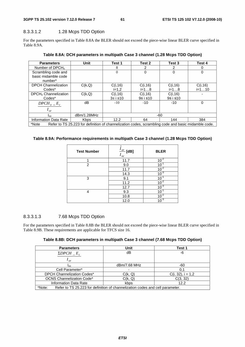
ETSI
ETSI TS 125 102 V7.12.0 (2008-10) 613GPP TS 25.102 version 7.12.0 Release 7
8.3.3.1.2 1.28 Mcps TDD Option
For the parameters specified in Table 8.8A the BLER should not exceed the piece-wise linear BLER curve specified in Table 8.9A.
Table 8.8A: DCH parameters in multipath Case 3 channel (1.28 Mcps TDD Option)
Parameters Unit Test 1 Test 2 Test 3 Test 4 Number of DPCHo 8 2 2 0
Scrambling code and basic midamble code
number*
0 0 0 0
DPCH Channelization Codes*
C(k,Q) C(i,16) i=1,2
C(i,16) i=1…8
C(i,16) i=1…8
C(i,16) i=1…10
DPCHo Channelization Codes*
C(k,Q) C(i,16) 3≤ i ≤10
C(i,16) 9≤ i ≤10
C(i,16) 9≤ i ≤10
-
or
co
I
EDPCH _
dB -10 -10 -10 0
Ioc dBm/1.28MHz -60 Information Data Rate Kbps 12.2 64 144 384 *Note Refer to TS 25.223 for definition of channelization codes, scrambling code and basic midamble code.
Table 8.9A: Performance requirements in multipath Case 3 channel (1.28 Mcps TDD Option)
Test Number oc
or
I
I[dB] BLER
1 11.7 10-2 9.0 10-1
11.7 10-2 2
14.3 10-3 9.1 10-1
11.2 10-2 3
12.7 10-3 9.3 10-1
10.8 10-2 4
12.0 10-3
8.3.3.1.3 7.68 Mcps TDD Option
For the parameters specified in Table 8.8B the BLER should not exceed the piece-wise linear BLER curve specified in Table 8.9B. These requirements are applicable for TFCS size 16.
Table 8.8B: DCH parameters in multipath Case 3 channel (7.68 Mcps TDD Option)
Parameters Unit Test 1
or
c
I
EDPCH _Σ
dB -6
Ioc dBm/7.68 MHz -60 Cell Parameter* - 0,1
DPCH Channelization Codes* C(k, Q) C(i, 32), i = 1,2 OCNS Channelization Code* C(k, Q) C(3, 32)
Information Data Rate kbps 12.2 *Note: Refer to TS 25.223 for definition of channelization codes and cell parameter.
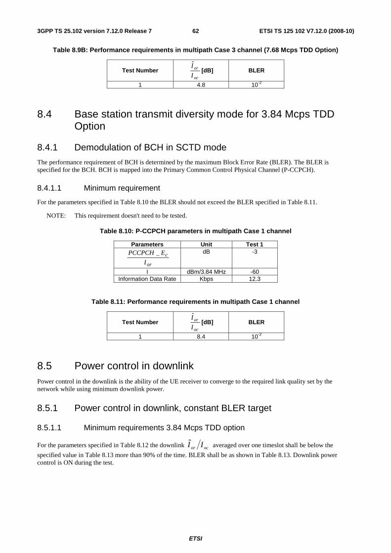
ETSI
ETSI TS 125 102 V7.12.0 (2008-10) 623GPP TS 25.102 version 7.12.0 Release 7
Table 8.9B: Performance requirements in multipath Case 3 channel (7.68 Mcps TDD Option)
Test Number oc
or
I
I[dB] BLER
1 4.8 10-2
8.4 Base station transmit diversity mode for 3.84 Mcps TDD Option
8.4.1 Demodulation of BCH in SCTD mode
The performance requirement of BCH is determined by the maximum Block Error Rate (BLER). The BLER is specified for the BCH. BCH is mapped into the Primary Common Control Physical Channel (P-CCPCH).
8.4.1.1 Minimum requirement
For the parameters specified in Table 8.10 the BLER should not exceed the BLER specified in Table 8.11.
NOTE: This requirement doesn't need to be tested.
Table 8.10: P-CCPCH parameters in multipath Case 1 channel
Parameters Unit Test 1
or
c
I
EPCCPCH _
dB -3
I dBm/3.84 MHz -60 Information Data Rate Kbps 12.3
Table 8.11: Performance requirements in multipath Case 1 channel
Test Number oc
or
I
I[dB] BLER
1 8.4 10-2
8.5 Power control in downlink Power control in the downlink is the ability of the UE receiver to converge to the required link quality set by the network while using minimum downlink power.
8.5.1 Power control in downlink, constant BLER target
8.5.1.1 Minimum requirements 3.84 Mcps TDD option
For the parameters specified in Table 8.12 the downlink ocor II averaged over one timeslot shall be below the
specified value in Table 8.13 more than 90% of the time. BLER shall be as shown in Table 8.13. Downlink power control is ON during the test.

ETSI
ETSI TS 125 102 V7.12.0 (2008-10) 633GPP TS 25.102 version 7.12.0 Release 7
Table 8.12: Test parameters for downlink power control - constant BLER Target (3.84 Mcps TDD option)
Parameter Unit Test 1
or
c
I
EDPCH _ dB 0
ocI dBm/3.84 MHz -60
Information Data Rate kbps 12.2 Target quality value on DTCH BLER 0.01
Propagation condition Case 1 DL Power Control step size, ΔTPC
dB 1
Maximum_DL_power * dB 0 Minimum_DL_power * dB -27 *Note: Refer to TS 25.224 for description and definition
Table 8.13: Requirements for downlink power control - constant BLER Target (3.84 Mcps TDD option)
Parameter Unit Test 1
ocor II dB 8.5
Measured quality on DTCH BLER 0.01±30%
8.5.1.2 Minimum requirements 1.28 Mcps TDD option
For the parameters specified in Table 8.13A the downlink ocor II averaged over one timeslot, shall be below the
specified value in Table 8.13B more than 90% of the time. BLER shall be as shown in table 8.13B. Downlink power control is ON during the test.
Table 8.13A: Test parameters for downlink power control - constant BLER Target (1.28 Mcps TDD option)
Parameter Unit Value
or
c
I
EDPCH _Σ dB 0
ocI dBm/1.28 Mhz -60
Information data rate kbps 12.2 Target quality on DTCH BLER 0.01
Propagation condition Case 1 DL Power Control step size, ΔTPC
dB 1
Maximum_DL_power * dB 0 Minimum_DL_power * dB -27
NOTE: Power is compared to P-CCPCH power
Table 8.13B: Requirements for downlink power control - constant BLER Target (1,28 Mcps TDD option)
Parameter Unit Value
ocor II dB 7.5
Measured quality on DTCH
BLER 0.01±30%

ETSI
ETSI TS 125 102 V7.12.0 (2008-10) 643GPP TS 25.102 version 7.12.0 Release 7
8.6 Uplink Power Control for 3.84 Mcps TDD Option Power control in the uplink is the ability of the UE to converge to the required link quality set by the network while using minimum uplink power.
8.6.1 Test Conditions
During period T1, the PCCPCH and a second Beacon Channel are transmitted in the DL in designated slots within each frame and at the same power level.
The UE transmits, using the channel of TS25.105, Annex A.2.1 UL reference measurement channel (12.2 kbps) in one UL slot. For different parts of the test, different UL slots will be designated.
The values of table 8.14, period T1 shall be selected. Then, with the received PCCPCH and Beacon power set at -60 dBm, the value of DPCH constant value shall be adjusted so that the mean UE output power is 5 dBm. These conditions are held steady during period T1.
Periods T1 and T2 are each 5 seconds long.
Table 8.14: UL Power Control Test Conditions
Period T1 Period T2 IBTS all slots dBm -60 PCCPCH Power -Broadcast dBm 18 PCCPCH power - Received dBm -60 -70 Mean UE transmit power dBm 5 According to tables
8.15 and 8.16 SIRTARGET dB 6 Ioc in PCCPCH and Beacon Slots dBm -60 IE (information element) Alpha As defined in
25.331 1.0
PCCPCH slot position Integer 0 -14 0 Beacon slot position Integer 0-14 8
T1 T2
Path Loss
Conditionsaccording to
8.14 period T1
Conditionsaccording to
8.14 period T28.15 and 8.16
10dB
Figure 8.1
8.6.2 Performance
At the end of period T1, the PCCPCH and Beacon Received power shall be simultaneously decreased by 10 dB. These conditions are summarized in table 8.14, period T2.
For the first frame including the change in received power the UE output power shall satisfy the values in table 8.15.
For the 20th frame after the change in received power the UE output power shall satisfy the values in table 8.16.

ETSI
ETSI TS 125 102 V7.12.0 (2008-10) 653GPP TS 25.102 version 7.12.0 Release 7
Table 8.15: Required UE Output Power, Frame Containing Power Level Change
Parameter Units Value UL transmission slot position 1,9 7,14 UE output power dBm 15 ±4.0 5 ±0.5
Table 8.16: Required UE Output Power, 20 Frames after Power Level Change
Parameter Units Value UL transmission slot position 1,9 7,14 UE output power dBm 15 ±4.0 15 ±4.0
9 Performance requirements (HSDPA)
9.1 Performance requirement for 3.84 Mcps TDD option The requirements are stated for the HSDPA UE reference combination classes specified in [2] and under the multipath propagation conditions specified in Annex B. The performance metric for HS-DSCH requirements in multi-path propagation conditions is the throughput R measured on HS-DSCH.
9.1.1 HS-DSCH throughput for fixed reference channels
The performance requirements in this subclause apply for the reference measurement channels specified in Annex A.3.2.
During the Fixed Reference Channel tests the behaviour of the Node-B emulator in response to the ACK/NACK signalling field of the HS-SICH is specified in Table 9.1:
Table 9.1: Node-B Emulator Behaviour in response to ACK/NACK/DTX
HS-SICH ACK/NACK Field State
Node-B Emulator Behaviour
ACK ACK: new transmission using 1st redundancy version (RV) NACK NACK: retransmission using the next RV (up to the maximum
permitted number or RV"s) DTX DTX: retransmission using the RV previously transmitted to
the same H-ARQ process
9.1.1.1 Minimum requirement QPSK, Fixed Reference Channel, 7,3 Mbps - Category 8 - UE
For the parameters specified in Table 9.2, the measured throughput R shall exceed the throughput specified in Table 9.3 for each radio condition.

ETSI
ETSI TS 125 102 V7.12.0 (2008-10) 663GPP TS 25.102 version 7.12.0 Release 7
Table 9.2: Test parameters for fixed reference measurement channel requirements for 7,3 Mbps - Category 8 - UE (3,84 Mcps TDD Option) QPSK
Parameters Unit Test 1 Test 2 Test 3 Test 4 HS-PDSCH Modulation - QPSK
Scrambling code and basic midamble code number* - 0, 1
Number of TS - 8 HS-PDSCH Channelization
Codes* C(k,Q) C(i,16) i=1..16
C(i,16) i=1..14
Number of Hybrid ARQ processes - 4
Maximum number of Hybrid ARQ transmissions - 4
Redundancy and constellation version coding sequence** - {0,0,0,0}
s=1, R=0, b=0
or
c
I
EPDSCHHS _− dB -12,04 -11.46
or
c
I
EPDSCHHS∑ − _ dB 0
Ioc dBm/3,84MHz
-60
Note *: Refer to TS 25.223 for definition of channelization codes, scrambling code and basic midamble code.
Note **: This sequence implies Chase combining
Table 9.3: Performance requirements for fixed reference measurement channel requirement in multipath channels for 7,3 Mbps - Category 8 - UE (3,84 Mcps TDD Option) QPSK
Test Number Propagation conditions
oc
or
I
I[dB] R (Throughput)
[kbps] 1 PA3 8,5 1300
2 PB3 9,0 1300 3 VA30 9,75 1300 4 VA120 11,5 1400
9.1.1.2 Minimum requirement 16QAM, Fixed Reference Channel, 7,3 Mbps - Category 8 - UE
For the parameters specified in Table 9.4, the measured throughput R shall exceed the throughput specified in Table 9.5 for each radio condition.

ETSI
ETSI TS 125 102 V7.12.0 (2008-10) 673GPP TS 25.102 version 7.12.0 Release 7
Table 9.4: Test parameters for fixed reference measurement channel requirements for 7,3 Mbps - Category 8 - UE (3,84 Mcps TDD Option) 16QAM
Parameters Unit Test 1 Test 2 Test 3 Test 4 HS-PDSCH Modulation - 16QAM
Scrambling code and basic midamble code number* - 0, 1
Number of TS - 8 HS-PDSCH Channelization
Codes* C(k,Q) C(i,16) i=1..16
C(i,16) i=1..14
Number of Hybrid ARQ processes - 4
Maximum number of Hybrid ARQ transmissions - 4
Redundancy and constellation version coding sequence** - {0,0,0,0}
s=1, r=0
or
c
I
EPDSCHHS _− dB -12,04 -11,46
or
c
I
EPDSCHHS∑ − _ dB 0
Ioc dBm/3,84MHz
-60
Note *: Refer to TS 25.223 for definition of channelization codes, scrambling code and basic midamble code.
Note **: This sequence implies Chase combining
Table 9.5: Performance requirements for fixed reference measurement channel requirement in multipath channels for 7,3 Mbps - Category 8 - UE (3,84 Mcps TDD Option) 16QAM
Test Number Propagation conditions
oc
or
I
I[dB] R (Throughput)
[kbps] 1 PA3 16,0 2600
2 PB3 17,5 2600 3 VA30 18,5 2600 4 VA120 14,5 1600
9.1.2 HS-DSCH throughput for Variable Reference Channels
9.1.2.1 Minimum requirement Variable Reference Channel, 7,3 Mbps - Category 8 - UE
For the parameters specified in Table 9.6 the measured throughput R shall exceed the throughput specified in Table 9.7 for each radio condition. The Variable Reference Channel is specified in Annex A.3.3.

ETSI
ETSI TS 125 102 V7.12.0 (2008-10) 683GPP TS 25.102 version 7.12.0 Release 7
Table 9.6: Test parameters for variable reference measurement channel requirements for 7,3 Mbps - Category 8 - UE (3,84 Mcps TDD Option)
Parameters Unit Test 1 Test 2 Test 3 Test 4 Scrambling code and basic
midamble code number* - 0, 1
Number of TS - 8 HS-PDSCH Channelization
Codes* C(k,Q) C(i,16) i=1..16
Number of Hybrid ARQ processes** - 4
Maximum number of Hybrid ARQ transmissions - 1
Redundancy and constellation version coding sequence
(Xrv, s, r, b) (0, 1, 0, 0)
HS-PDSCHi_Ec/Ior dB -12,04
_1
Ior
EcPDSCHHSi
i∑ − dB 0
Ioc dBm/3,84MHz -60 Note *: Refer to TS 25.223 for definition of channelization codes, scrambling code and basic
midamble code. Note **: For timing requirements, HARQ is not active
Table 9.7: Performance requirements for variable reference measurement channel requirement in multipath channels for 7,3 Mbps - Category 8 - UE (3,84 Mcps TDD Option)
Test Number Propagation conditions
oc
or
I
I[dB] R (Throughput)
[kbps] 1 PA3 8,8 1240
14,8 2500 18,8 3600 24,8 5000
2 PB3 8,8 1220 14,8 2430 20,8 4030 24,8 5080
3 VA30 10,1 1190 16,1 2290 20,1 3220 24,1 4260
4 VA120 7,1 590 11,1 1180 15,1 1840 19,1 2390
9.1.3 Reporting of Channel Quality Indicator
The reporting accuracy of channel quality indicator (CQI) under AWGN environments is determined by the reporting variance and BLER performance using the transport format indicated by the reported median CQI.
9.1.3.1 Minimum requirement Channel Quality Indicator, 7,3 Mbps - Category 8 - UE
For the parameters specified in Table 9.7A the reported CQI value shall be within the range of +/- 10 of the allowable CQIs of the reported median CQI more than 90% of the time. The BLER for the reported median CQI shall be less than 10%.
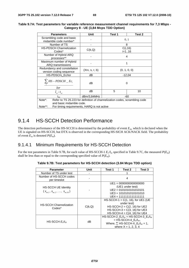
ETSI
ETSI TS 125 102 V7.12.0 (2008-10) 693GPP TS 25.102 version 7.12.0 Release 7
Table 9.7A: Test parameters for variable reference measurement channel requirements for 7,3 Mbps - Category 8 - UE (3,84 Mcps TDD Option)
Parameters Unit Test 1 Test 2 Scrambling code and basic
midamble code number* - 0, 1
Number of TS - 8 HS-PDSCH Channelization
Codes* C(k,Q) C(i,16) i=1..16
Number of Hybrid ARQ processes** - 4
Maximum number of Hybrid ARQ transmissions - 1
Redundancy and constellation version coding sequence
(Xrv, s, r, b) (0, 1, 0, 0)
HS-PDSCHi_Ec/Ior dB -12,04
_1
Ior
EcPDSCHHSi
i∑ − dB 0
ˆ /or ocI I dB 5 10
Ioc dBm/3,84MHz -60 Note*: Refer to TS 25.223 for definition of channelization codes, scrambling code
and basic midamble code. Note**: For timing requirements, HARQ is not active
9.1.4 HS-SCCH Detection Performance The detection performance of the HS-SCCH is determined by the probability of event Em, which is declared when the UE is signaled on HS-SCCH, but DTX is observed in the corresponding HS-SICH ACK/NACK field. The probability of event Em is denoted P(Em).
9.1.4.1 Minimum Requirements for HS-SCCH Detection
For the test parameters in Table 9.7B, for each value of HS-SCCH-1 Ec/Ior specified in Table 9.7C, the measured P(Em) shall be less than or equal to the corresponding specified value of P(Em).
Table 9.7B: Test parameters for HS-SCCH detection (3.84 Mcps TDD option)
Parameter Unit Test 1 Test 2 Test 3 Number of TS under test - 1
Number of HS-SCCH codes per timeslot - 4
HS-SCCH UE Identity ( ,1uex , ,2uex , …, ,16uex ) -
UE1 = 0000000000000000 (UE1 under test)
UE2 = 0101010101010101 UE3 = 1010101010101010 UE4 = 1111111111111111
HS-SCCH Channelization Codes* C(k,Q)
HS-SCCH-1 = C(1, 16), for UE1 (UE under test)
HS-SCCH-2 = C(2, 16) for UE2 HS-SCCH-3 = C(3, 16) for UE3 HS-SCCH-4 = C(4, 16) for UE4
HS-SCCH Ec/Ior dB
HS-SCCH-2_Ec/Ior = HS-SCCH-3_Ec/Ior = HS-SCCH-4_Ec/Ior,
Where, ∑ HS-SCCH-X_Ec/Ior = 1, where X = 1, 2, 3, 4

ETSI
ETSI TS 125 102 V7.12.0 (2008-10) 703GPP TS 25.102 version 7.12.0 Release 7
Table 9.7C: Minimum requirement for HS-SCCH detection (3.84 Mcps TDD option)
Reference value Test Number
Propagation Conditions HS-SCCH-1
/c orE I (dB) ˆ /or ocI I (dB) ( )mP E
1 PA3 -1.6 0 0.05 2 PA3 -3.0 5 0.01 3 VA30 -2.5 0 0.01
9.2 Performance requirements for 1.28 Mcps TDD option The requirements are stated for the HSDPA UE reference combination classes specified in [2] and under the multipath propagation conditions specified in Annex B. The performance metric for HS-DSCH requirements in multi-path propagation conditions is the throughput R measured on HS-DSCH.
9.2.1 HS-DSCH throughput for fixed reference channels
The performance requirements in this subclause apply for the reference measurement channels specified in Annex A.3.2.
During the Fixed Reference Channel tests the behaviour of the Node-B emulator in response to the ACK/NACK signalling field of the HS-SICH is specified in Table 9.8
Table 9.8: Node-B Emulator Behaviour in response to ACK/NACK/DTX
HS-SICH ACK/NACK Field State
Node-B Emulator Behaviour
ACK ACK: new transmission using 1st redundancy and constellation version (RV)
NACK NACK: retransmission using the next RV (up to the maximum permitted number or RV"s)
DTX DTX: retransmission using the RV previously transmitted to the same H-ARQ process
NOTE: Performance requirements in this section assume a sufficient power allocation to HS-SCCH so that probability of reporting DTX is very low.
9.2.1.1 Category 1, 0.5Mbps UE class
For the parameters specified in Table 9.9, the measured throughput R shall exceed the throughput specified in Table 9.10 for each radio condition.
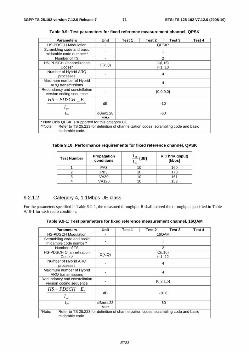
ETSI
ETSI TS 125 102 V7.12.0 (2008-10) 713GPP TS 25.102 version 7.12.0 Release 7
Table 9.9: Test parameters for fixed reference measurement channel, QPSK
Parameters Unit Test 1 Test 2 Test 3 Test 4 HS-PDSCH Modulation - QPSK*
Scrambling code and basic midamble code number** - 1
Number of TS - 2 HS-PDSCH Channelization
Codes* C(k,Q) C(i,16) i=1..10
Number of Hybrid ARQ processes - 4
Maximum number of Hybrid ARQ transmissions
- 4
Redundancy and constellation version coding sequence - {0,0,0,0}
or
c
I
EPDSCHHS _− dB -10
Ioc dBm/1.28MHz
-60
* Note Only QPSK is supported for this category UE. **Note: Refer to TS 25.223 for definition of channelization codes, scrambling code and basic
midamble code.
Table 9.10: Performance requirements for fixed reference channel, QPSK
Test Number Propagation conditions
oc
or
I
I[dB] R (Throughput)
[kbps] 1 PA3 10 160
2 PB3 10 170 3 VA30 10 161 4 VA120 10 153
9.2.1.2 Category 4, 1.1Mbps UE class
For the parameters specified in Table 9.9-1, the measured throughput R shall exceed the throughput specified in Table 9.10-1 for each radio condition.
Table 9.9-1: Test parameters for fixed reference measurement channel, 16QAM
Parameters Unit Test 1 Test 2 Test 3 Test 4 HS-PDSCH Modulation - 16QAM
Scrambling code and basic midamble code number* - 1
Number of TS - 2 HS-PDSCH Channelization
Codes* C(k,Q) C(i,16) i=1..12
Number of Hybrid ARQ processes
- 4
Maximum number of Hybrid ARQ transmissions - 4
Redundancy and constellation version coding sequence - {6,2,1,5}
or
c
I
EPDSCHHS _− dB -10.8
Ioc dBm/1.28MHz
-60
*Note: Refer to TS 25.223 for definition of channelization codes, scrambling code and basic midamble code.

ETSI
ETSI TS 125 102 V7.12.0 (2008-10) 723GPP TS 25.102 version 7.12.0 Release 7
Table 9.10-1: Performance requirements for QPSK, fixed reference channel, 16QAM
Test Number Propagation conditions
oc
or
I
I[dB] R (Throughput)
[kbps] 1 PA3 15 388
2 PB3 15 347 3 VA30 15 316 4 VA120 15 274
* Note: Test case in 9.2.1.1.1 can be used to test this kind of UE in case of QPSK.
9.2.1.3 Category 7, 1.6Mbps UE class
For the parameters specified in Table 9.9-2, the measured throughput R shall exceed the throughput specified in Table 9.10-2 for each radio condition.
Table 9.9-2: Test parameters for fixed reference measurement channel
Parameters Unit Test 1 Test 2 Test 3 Test 4 Test 5 Test 6 Test 7 Test 8 HS-PDSCH Modulation - QPSK 16QAM Scrambling code and basic midamble code
number* - 1
Number of TS - 3 Number of Hybrid ARQ
processes - 4
Maximum number of Hybrid ARQ
transmissions - 4
HS-PDSCH Channelization Codes* C(k,Q) C(i,16)
i=1..10 C(i,16) i=1..12
Redundancy and constellation version
coding sequence - {0,0,0,0} {6,2,1,5}
or
c
I
EPDSCHHS _− dB -10 -10.8
Ioc dBm/ 1.28MHz
-60
*Note: Refer to TS 25.223 for definition of channelization codes, scrambling code and basic midamble code.
Table 9.10-2: Performance requirements for fixed reference channel
Test Number Propagation conditions
oc
or
I
I[dB] R (Throughput)
[kbps] 1 PA3 10 270
2 PB3 10 278 3 VA30 10 259 4 VA120 10 242 5 PA3 15 488 6 PB3 15 471 7 VA30 15 431 8 VA120 15 377
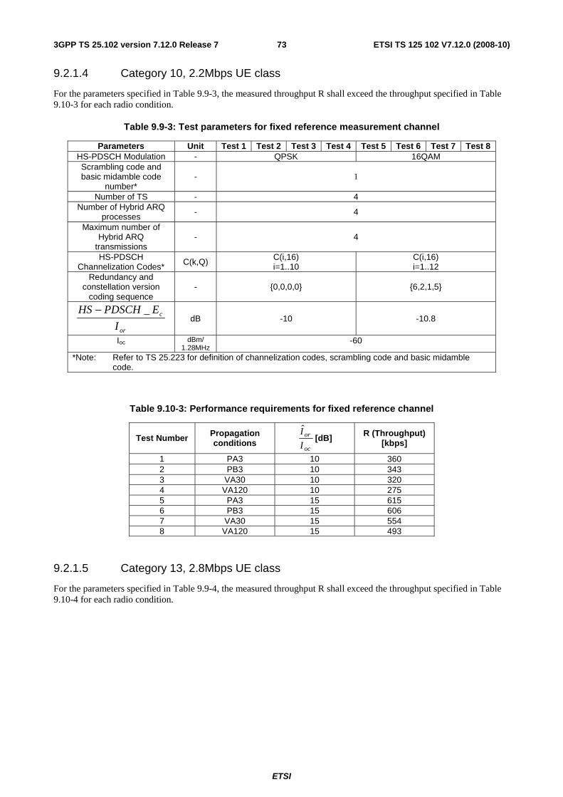
ETSI
ETSI TS 125 102 V7.12.0 (2008-10) 733GPP TS 25.102 version 7.12.0 Release 7
9.2.1.4 Category 10, 2.2Mbps UE class
For the parameters specified in Table 9.9-3, the measured throughput R shall exceed the throughput specified in Table 9.10-3 for each radio condition.
Table 9.9-3: Test parameters for fixed reference measurement channel
Parameters Unit Test 1 Test 2 Test 3 Test 4 Test 5 Test 6 Test 7 Test 8 HS-PDSCH Modulation - QPSK 16QAM Scrambling code and basic midamble code
number* - 1
Number of TS - 4 Number of Hybrid ARQ
processes - 4
Maximum number of Hybrid ARQ
transmissions - 4
HS-PDSCH Channelization Codes* C(k,Q) C(i,16)
i=1..10 C(i,16) i=1..12
Redundancy and constellation version
coding sequence - {0,0,0,0} {6,2,1,5}
or
c
I
EPDSCHHS _− dB -10 -10.8
Ioc dBm/ 1.28MHz
-60
*Note: Refer to TS 25.223 for definition of channelization codes, scrambling code and basic midamble code.
Table 9.10-3: Performance requirements for fixed reference channel
Test Number Propagation conditions
oc
or
I
I[dB] R (Throughput)
[kbps] 1 PA3 10 360
2 PB3 10 343 3 VA30 10 320 4 VA120 10 275 5 PA3 15 615 6 PB3 15 606 7 VA30 15 554 8 VA120 15 493
9.2.1.5 Category 13, 2.8Mbps UE class
For the parameters specified in Table 9.9-4, the measured throughput R shall exceed the throughput specified in Table 9.10-4 for each radio condition.
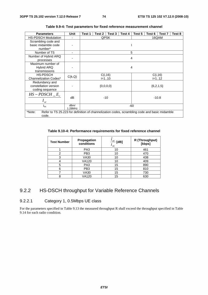
ETSI
ETSI TS 125 102 V7.12.0 (2008-10) 743GPP TS 25.102 version 7.12.0 Release 7
Table 9.9-4: Test parameters for fixed reference measurement channel
Parameters Unit Test 1 Test 2 Test 3 Test 4 Test 5 Test 6 Test 7 Test 8 HS-PDSCH Modulation - QPSK 16QAM Scrambling code and basic midamble code
number* - 1
Number of TS - 5 Number of Hybrid ARQ
processes - 4
Maximum number of Hybrid ARQ
transmissions - 4
HS-PDSCH Channelization Codes* C(k,Q) C(i,16)
i=1..10 C(i,16) i=1..12
Redundancy and constellation version
coding sequence - {0,0,0,0} {6,2,1,5}
or
c
I
EPDSCHHS _− dB -10 -10.8
Ioc dBm/ 1.28MHz
-60
*Note: Refer to TS 25.223 for definition of channelization codes, scrambling code and basic midamble code.
Table 9.10-4: Performance requirements for fixed reference channel
Test Number Propagation conditions
oc
or
I
I[dB] R (Throughput)
[kbps] 1 PA3 10 461
2 PB3 10 470 3 VA30 10 438 4 VA120 10 409 5 PA3 15 890 6 PB3 15 810 7 VA30 15 730 8 VA120 15 630
9.2.2 HS-DSCH throughput for Variable Reference Channels
9.2.2.1 Category 1, 0.5Mbps UE class
For the parameters specified in Table 9.13 the measured throughput R shall exceed the throughput specified in Table 9.14 for each radio condition.

ETSI
ETSI TS 125 102 V7.12.0 (2008-10) 753GPP TS 25.102 version 7.12.0 Release 7
Table 9.13: Test parameters for variable reference channel, 0.5Mbps UE class
Parameter Unit Test 1 Test 2 Test 3 HS-PDSCH Modulation
and TBS - *
Scrambling code and basic midamble code
Number ** -
1
Number of TS - 2 Number of DPCHo - 0 Number of HARQ
Process - 4
Number of transmission - 1 Redundancy and
constellation version coding sequence
Xrv 0
HS-DSCH Channelization Codes**
C(k,Q) C(i,16) 1≤i≤10
HS-DSCHi_Ec/Ior dB -10 Ioc dBm -60
* Note 1 As requested by the last received CQI report **Note 2 Refer to TS 25.223 for definition of channelization codes, scrambling code and basic
midamble code. ***Note 3 If the indicated CQI is 0, the Node-B emulator shall format the next HS-PDSCH
transmission with the transport block size and the modulation scheme that were previously used.
Table 9.14: Performance requirements for variable reference channel, 0.5Mbps UE class
Test Number Propagation conditions
oc
or
I
I[dB] R (Throughput)
[kbps] 1 PA3 15 242
2 PB3 15 244 3 VA30 15 211
9.2.2.2 Category 4, 1.1Mbps UE class
For the parameters specified in Table 9.13-1 the measured throughput R shall exceed the throughput specified in Table 9.14-1 for each radio condition.

ETSI
ETSI TS 125 102 V7.12.0 (2008-10) 763GPP TS 25.102 version 7.12.0 Release 7
Table 9.13-1: Test parameters for variable reference channel, 1.1Mbps UE class
Parameter Unit Test 1 Test 2 Test 3 HS-PDSCH Modulation
and TBS - *
Scrambling code and basic midamble code
Number ** -
1
Number of TS - 2 Number of DPCHo - 0 Number of HARQ
Process - 4
Number of transmission - 1 Redundancy and
constellation version coding sequence
Xrv 0
HS-DSCH Channelization Codes**
C(k,Q) C(i,16) 1≤i≤10
HS-DSCHi_Ec/Ior dB -10 Ioc dBm -60
* Note 1 As requested by the last received CQI report **Note 2 Refer to TS 25.223 for definition of channelization codes, scrambling code and basic
midamble code. ***Note 3 If the indicated CQI is 0, the Node-B emulator shall format the next HS-PDSCH
transmission with the transport block size and the modulation scheme that were previously used.
Table 9.14-1: Performance requirements for variable reference channel, 1.1 Mbps UE class
Test Number Propagation conditions
oc
or
I
I[dB] R (Throughput)
[kbps] 1 PA3 15 318
2 PB3 15 323 3 VA30 15 213
9.2.2.3 Category 7, 1.6Mbps UE class
For the parameters specified in Table 9.13-2 the measured throughput R shall exceed the throughput specified in Table 9.14-2 for each radio condition.

ETSI
ETSI TS 125 102 V7.12.0 (2008-10) 773GPP TS 25.102 version 7.12.0 Release 7
Table 9.13-2: Test parameters for variable reference channel, 1.6Mbps UE class
Parameter Unit Test 1 Test 2 Test 3 HS-PDSCH Modulation
and TBS - *
Scrambling code and basic midamble code
Number ** -
1
Number of TS - 3 Number of DPCHo - 0 Number of HARQ
Process - 4
Number of transmission - 1 Redundancy and
constellation version coding sequence
Xrv 0
HS-DSCH Channelization Codes**
C(k,Q) C(i,16) 1≤i≤10
HS-DSCHi_Ec/Ior dB -10 Ioc dBm -60
* Note 1 As requested by the last received CQI report **Note 2 Refer to TS 25.223 for definition of channelization codes, scrambling code and basic
midamble code. ***Note 3 If the indicated CQI is 0, the Node-B emulator shall format the next HS-PDSCH
transmission with the transport block size and the modulation scheme that were previously used.
Table 9.14-2: Performance requirements for variable reference channel, 1.6Mbps UE class
Test Number Propagation conditions
oc
or
I
I[dB] R (Throughput)
[kbps] 1 PA3 15 480
2 PB3 15 483 3 VA30 15 323
9.2.2.4 Category 10, 2.2 Mbps UE class
For the parameters specified in Table 9.13-3 the measured throughput R shall exceed the throughput specified in Table 9.14-3 for each radio condition.
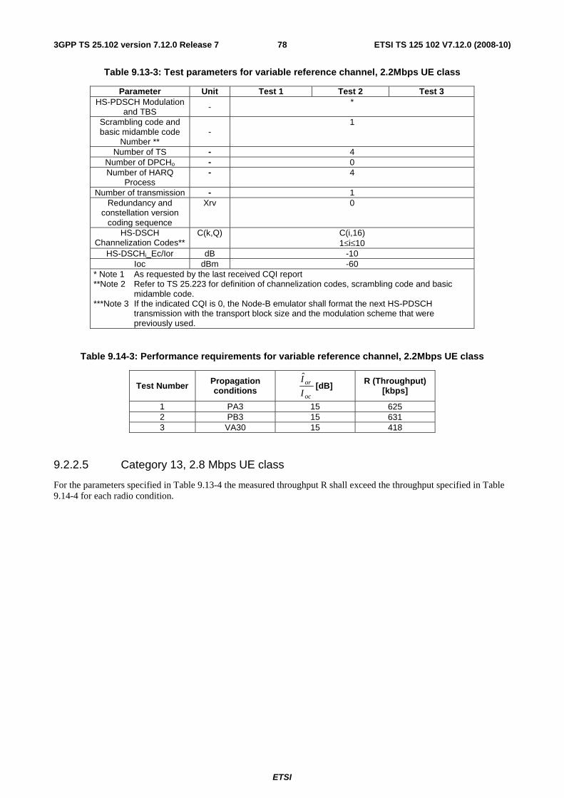
ETSI
ETSI TS 125 102 V7.12.0 (2008-10) 783GPP TS 25.102 version 7.12.0 Release 7
Table 9.13-3: Test parameters for variable reference channel, 2.2Mbps UE class
Parameter Unit Test 1 Test 2 Test 3 HS-PDSCH Modulation
and TBS - *
Scrambling code and basic midamble code
Number ** -
1
Number of TS - 4 Number of DPCHo - 0 Number of HARQ
Process - 4
Number of transmission - 1 Redundancy and
constellation version coding sequence
Xrv 0
HS-DSCH Channelization Codes**
C(k,Q) C(i,16) 1≤i≤10
HS-DSCHi_Ec/Ior dB -10 Ioc dBm -60
* Note 1 As requested by the last received CQI report **Note 2 Refer to TS 25.223 for definition of channelization codes, scrambling code and basic
midamble code. ***Note 3 If the indicated CQI is 0, the Node-B emulator shall format the next HS-PDSCH
transmission with the transport block size and the modulation scheme that were previously used.
Table 9.14-3: Performance requirements for variable reference channel, 2.2Mbps UE class
Test Number Propagation conditions
oc
or
I
I[dB] R (Throughput)
[kbps] 1 PA3 15 625
2 PB3 15 631 3 VA30 15 418
9.2.2.5 Category 13, 2.8 Mbps UE class
For the parameters specified in Table 9.13-4 the measured throughput R shall exceed the throughput specified in Table 9.14-4 for each radio condition.

ETSI
ETSI TS 125 102 V7.12.0 (2008-10) 793GPP TS 25.102 version 7.12.0 Release 7
Table 9.13-4: Test parameters for variable reference channel, 2.8Mbps UE class
Parameter Unit Test 1 Test 2 Test 3 HS-PDSCH Modulation
and TBS - *
Scrambling code and basic midamble code
Number ** -
1
Number of TS - 2 Number of DPCHo - 0 Number of HARQ
Process - 4
Number of transmission - 1 Redundancy and
constellation version coding sequence
Xrv 0
HS-DSCH Channelization Codes**
C(k,Q) C(i,16) 1≤i≤10
HS-DSCHi_Ec/Ior dB -10 Ioc dBm -60
* Note 1 As requested by the last received CQI report **Note 2 Refer to TS 25.223 for definition of channelization codes, scrambling code and basic
midamble code. ***Note 3 If the indicated CQI is 0, the Node-B emulator shall format the next HS-PDSCH
transmission with the transport block size and the modulation scheme that were previously used.
Table 9.14-4: Performance requirements for variable reference channel, 2.8 Mbps UE class
Test Number Propagation conditions
oc
or
I
I[dB] R (Throughput)
[kbps] 1 PA3 15 783
2 PB3 15 792 3 VA30 15 544
9.2.3 Reporting of Channel Quality Indicator The reporting accuracy of channel quality indicator (CQI) under AWGN environments is determined by the reporting variance and the BLER performance using the transport format indicated by the reported CQI median.
9.2.3.1 Minimum Requirement, Channel Quality Indicator - 1.4Mbps UE class
For the parameters specified in Table 9.15, the reported CQI value shall be within +/- x, as specified in Table 9.16, of the reported median CQI for more than Y%, also specified in Table 9.16, of the time.

ETSI
ETSI TS 125 102 V7.12.0 (2008-10) 803GPP TS 25.102 version 7.12.0 Release 7
Table 9.15: Test parameters for CQI reporting measurement channel requirements (1.28 Mcps TDD Option)
0.5Mbps UE 1.1Mbps UE
1.6Mbps UE
2.2Mbps UE
2.8Mbps UE
Parameter Unit Test 1 Test 2
Test 3
Test 4
Test 5
Test 6
Test 7
Test 8
Test9
Number of TS - 2 2 3 4 5 Number of HS-PDSCH codes
per TS
- 10 10 10 10 10
HS-DSCHi_Ec/Ior dB -10 -10 -10 -10 -10
HS-DSCH Channelization
Codes*
C(k,Q)
C(i,16) 1≤i≤10
C(i,16) 1≤i≤10
C(i,16) 1≤i≤10
C(i,16) 1≤i≤10
C(i,16) 1≤i≤10
Number of DPCHo
- 0
Number of HARQ Process
- 4
Number of transmission
- 1
ˆ /or ocI I dB 1 1 8 1 8 1 8 1 8
Table 9.16: Performance requirements for CQI reporting measurement channel requirements (1.28 Mcps TDD Option)
Test Permitted CQI
range from median (x)
% of time that CQI must be within +/- x of
median (Y)
Maximum BLER for median
reported CQI Test 1 +/- 3 90 Test 2 +/- 3 90 Test 3 +/- 2 90 Test 4 +/- 2 90 Test 5 +/-2 90 Test 6 +/-2 90 Test 7 +/-2 90 Test 8 +/-2 90 Test 9 +/-2 90
10%
9.2.4 HS-SCCH Detection Performance The detection performance of the HS-SCCH is determined by the probability of event Em, which is declared when the UE is signaled on HS-SCCH, but DTX is observed in the corresponding HS-SICH ACK/NACK field. The probability of event Em is denoted P(Em).
9.2.4.1 Minimum Requirements for HS-SCCH Detection
For the test parameters specified in Table 9.17, for each value of HS-SCCH ocor II specified in Table 9.18 the
measured P(Em) shall be less than or equal to the corresponding specified value of P(Em).

ETSI
ETSI TS 125 102 V7.12.0 (2008-10) 813GPP TS 25.102 version 7.12.0 Release 7
Table 9.17: Test parameters for HS-SCCH detection (1.28Mcps TDD option)
Parameter Unit Test 1 Test2 Number of TS under test - 1
Number of HS-SCCH codes per timeslot - 8 (4 x2)
Scrambling code and basic midamble code number* - 0
Number of DPCHo - 2 Number of H-ARQ process - 4
HS-SCCH UE Identity ( ,1uex , ,2uex , …, ,16uex ) -
UE1 = 0000000000000000 (UE1 under test)
UE2 = 0101010101010101 UE3 = 1010101010101010 UE4 = 1111111111111111
HS-SCCH Channelization Codes* C(k,Q)
C(i,16) 1≤i≤8
HS-SCCH Channelization Codes for UE under test C(k,Q)
C(i,16) 1≤i≤2
DPCHo Channelization Codes C(k,Q) C(i,16) 9≤i≤10
Power control for HS-SCCH of UE 1
- OFF
or
ci
I
ESCCHHS _− dB -10
Ioc dBm/1.28MHz -60 Note *: Refer to TS 25.223 for definition of channelization codes, scrambling code and
basic midamble code.
Table 9.18: Minimum requirement for HS-SCCH detection (1.28Mcps TDD option)
Test Number
Propagation Conditions
oc
or
I
I(dB) ( )mP E
1 PA3 16 0.01 2 VA30 12 0.01
9.2.5 PLCCH Detection Performance The detection performance of the PLCCH is determined by the BER of the received PLCCH.
9.2.4.1 Minimum Requirements
For the test parameters in Table 9.18A, for the value of Îor/Ioc specified in Table 9.18B, the measured BER should be equal or less than the corresponding specified BER value.

ETSI
ETSI TS 125 102 V7.12.0 (2008-10) 823GPP TS 25.102 version 7.12.0 Release 7
Table 9.18A: Test parameters for PLCCH detection (1.28Mcps TDD option)
Parameter Unit Test 1 Number of PLCCH - 1 Number of interfering codes/timeslot - 1 × SF16 Number of timeslot - 1 PLCCH information bit pattern - Alternating 1 and 0 starting
with 1 (101010….) Ioc dBm/1.28 MHz -60 PLCCH_Ec/Ior dB -3 PLCCH channelization codes C(k, Q) C(1, 16) OCNS channelization code C(k, Q) C(2, 16) Midamble allocation - Common Power control - OFF Propagation condition - VA30
Table 9.18B: Minimum requirement for PLCCH detection (1.28Mcps TDD option)
Test Number
oc
or
I
I(dB) BER
1 0.3 0.04
9.3 Performance requirement for 7.68 Mcps TDD option The requirements are stated for the HSDPA UE reference combination classes specified in [2] and under the multipath propagation conditions specified in Annex B. The performance metric for HS-DSCH requirements in multi-path propagation conditions is the throughput R measured on HS-DSCH.
9.3.1 HS-DSCH throughput for fixed reference channels
The performance requirements in this subclause apply for the reference measurement channels specified in Annex A.3.2.
During the Fixed Reference Channel tests the behaviour of the Node-B emulator in response to the ACK/NACK signalling field of the HS-SICH is specified in Table 9.19:
Table 9.19: Node-B Emulator Behaviour in response to ACK/NACK/DTX
HS-SICH ACK/NACK Field State
Node-B Emulator Behaviour
ACK ACK: new transmission using 1st redundancy version (RV) NACK NACK: retransmission using the next RV (up to the maximum
permitted number or RV"s) DTX DTX: retransmission using the RV previously transmitted to
the same H-ARQ process
9.3.1.1 Minimum requirement QPSK, Fixed Reference Channel, 5,3 Mbps - Category 8 - UE
For the parameters specified in Table 9.20, the measured throughput R shall exceed the throughput specified in Table 9.21 for each radio condition.
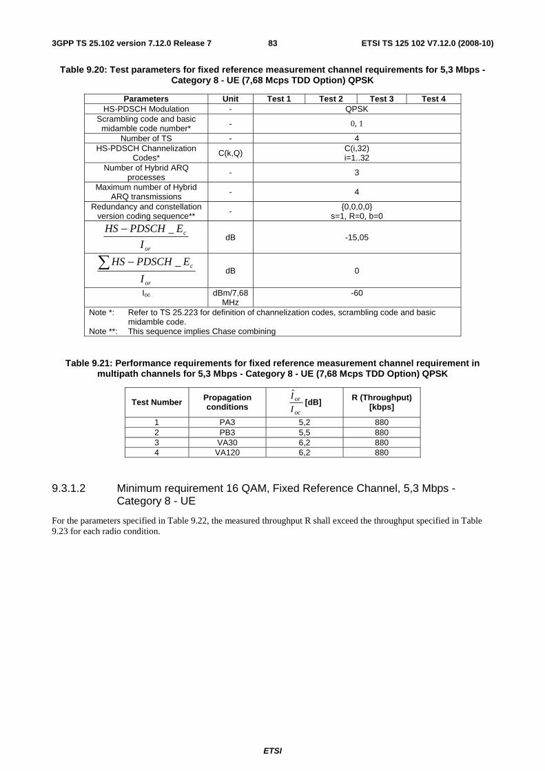
ETSI
ETSI TS 125 102 V7.12.0 (2008-10) 833GPP TS 25.102 version 7.12.0 Release 7
Table 9.20: Test parameters for fixed reference measurement channel requirements for 5,3 Mbps - Category 8 - UE (7,68 Mcps TDD Option) QPSK
Parameters Unit Test 1 Test 2 Test 3 Test 4 HS-PDSCH Modulation - QPSK
Scrambling code and basic midamble code number* - 0, 1
Number of TS - 4 HS-PDSCH Channelization
Codes* C(k,Q) C(i,32) i=1..32
Number of Hybrid ARQ processes - 3
Maximum number of Hybrid ARQ transmissions - 4
Redundancy and constellation version coding sequence** - {0,0,0,0}
s=1, R=0, b=0
or
c
I
EPDSCHHS _− dB -15,05
or
c
I
EPDSCHHS∑ − _ dB 0
Ioc dBm/7,68MHz
-60
Note *: Refer to TS 25.223 for definition of channelization codes, scrambling code and basic midamble code.
Note **: This sequence implies Chase combining
Table 9.21: Performance requirements for fixed reference measurement channel requirement in multipath channels for 5,3 Mbps - Category 8 - UE (7,68 Mcps TDD Option) QPSK
Test Number Propagation conditions
oc
or
I
I[dB] R (Throughput)
[kbps] 1 PA3 5,2 880
2 PB3 5,5 880 3 VA30 6,2 880 4 VA120 6,2 880
9.3.1.2 Minimum requirement 16 QAM, Fixed Reference Channel, 5,3 Mbps - Category 8 - UE
For the parameters specified in Table 9.22, the measured throughput R shall exceed the throughput specified in Table 9.23 for each radio condition.
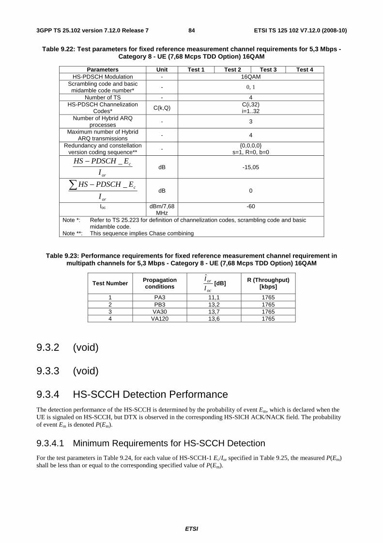
ETSI
ETSI TS 125 102 V7.12.0 (2008-10) 843GPP TS 25.102 version 7.12.0 Release 7
Table 9.22: Test parameters for fixed reference measurement channel requirements for 5,3 Mbps - Category 8 - UE (7,68 Mcps TDD Option) 16QAM
Parameters Unit Test 1 Test 2 Test 3 Test 4 HS-PDSCH Modulation - 16QAM
Scrambling code and basic midamble code number* - 0, 1
Number of TS - 4 HS-PDSCH Channelization
Codes* C(k,Q) C(i,32) i=1..32
Number of Hybrid ARQ processes - 3
Maximum number of Hybrid ARQ transmissions - 4
Redundancy and constellation version coding sequence** - {0,0,0,0}
s=1, R=0, b=0
or
c
I
EPDSCHHS _− dB -15,05
or
c
I
EPDSCHHS∑ − _ dB 0
Ioc dBm/7,68MHz
-60
Note *: Refer to TS 25.223 for definition of channelization codes, scrambling code and basic midamble code.
Note **: This sequence implies Chase combining
Table 9.23: Performance requirements for fixed reference measurement channel requirement in multipath channels for 5,3 Mbps - Category 8 - UE (7,68 Mcps TDD Option) 16QAM
Test Number Propagation conditions
oc
or
I
I[dB] R (Throughput)
[kbps] 1 PA3 11,1 1765
2 PB3 13,2 1765 3 VA30 13,7 1765 4 VA120 13,6 1765
9.3.2 (void)
9.3.3 (void)
9.3.4 HS-SCCH Detection Performance The detection performance of the HS-SCCH is determined by the probability of event Em, which is declared when the UE is signaled on HS-SCCH, but DTX is observed in the corresponding HS-SICH ACK/NACK field. The probability of event Em is denoted P(Em).
9.3.4.1 Minimum Requirements for HS-SCCH Detection
For the test parameters in Table 9.24, for each value of HS-SCCH-1 Ec/Ior specified in Table 9.25, the measured P(Em) shall be less than or equal to the corresponding specified value of P(Em).

ETSI
ETSI TS 125 102 V7.12.0 (2008-10) 853GPP TS 25.102 version 7.12.0 Release 7
Table 9.24: Test parameters for HS-SCCH detection (7.68 Mcps TDD option)
Parameter Unit Test 1 Test 2 Test 3 Number of TS under test - 1
Number of HS-SCCH codes per timeslot - 4
HS-SCCH UE Identity ( ,1uex , ,2uex , …, ,16uex ) -
UE1 = 0000000000000000 (UE1 under test)
UE2 = 0101010101010101 UE3 = 1010101010101010 UE4 = 1111111111111111
HS-SCCH Channelization Codes* C(k,Q)
HS-SCCH-1 = C(1, 32), for UE1 (UE under test)
HS-SCCH-2 = C(2, 32) for UE2 HS-SCCH-3 = C(3, 32) for UE3 HS-SCCH-4 = C(4, 32) for UE4
HS-SCCH Ec/Ior dB
HS-SCCH-2_Ec/Ior = HS-SCCH-3_Ec/Ior = HS-SCCH-4_Ec/Ior,
Where, ∑ HS-SCCH-X_Ec/Ior = 1, where X = 1, 2, 3, 4
Table 9.25: Minimum requirement for HS-SCCH detection (7.68 Mcps TDD option)
Reference value Test Number
Propagation Conditions HS-SCCH-1
/c orE I (dB) ˆ /or ocI I (dB) ( )mP E
1 PA3 -6.0 0 0.05 2 PA3 -7.5 5 0.01 3 VA30 -6.0 0 0.01
10 Performance requirements (MBMS)
10.1 Demodulation of MCCH The receive characteristic of the MCCH is determined by the RLC SDU error rate (RLC_SDU_ER). The requirement is valid for all RRC states for which the UE has capabilities.
10.1.1 Minimum requirement
10.1.1.1 3.84 Mcps TDD Option
For the parameters specified in Table 10.1, the measured average downlink S-CCPCH_Ec/Ior power ratio shall be below the specified value for the RLC_SDU_ER shown in Table 10.2.
Table 10.1: Test parameters for MCCH detection
Parameters Unit Test 1 Ioc dBm/3.84 MHz -60
oc
or
I
I
dB -3
Number of Interfering codes/timeslot
- 7 × SF16
MCCH Data Rate kbps 7.2 Propagation condition - VA3
Slot Format #i - 3
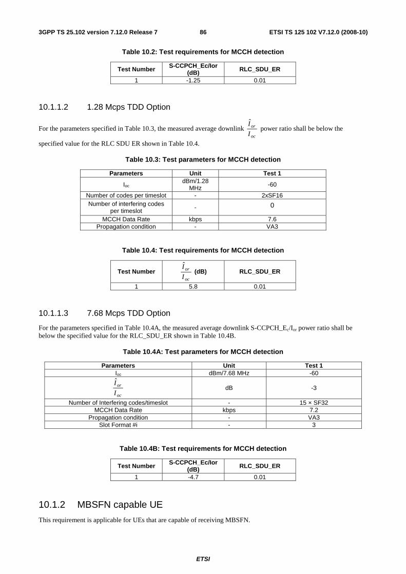
ETSI
ETSI TS 125 102 V7.12.0 (2008-10) 863GPP TS 25.102 version 7.12.0 Release 7
Table 10.2: Test requirements for MCCH detection
Test Number S-CCPCH_Ec/Ior (dB) RLC_SDU_ER
1 -1.25 0.01
10.1.1.2 1.28 Mcps TDD Option
For the parameters specified in Table 10.3, the measured average downlink oc
or
I
I
power ratio shall be below the
specified value for the RLC SDU ER shown in Table 10.4.
Table 10.3: Test parameters for MCCH detection
Parameters Unit Test 1
Ioc dBm/1.28
MHz -60
Number of codes per timeslot - 2xSF16 Number of interfering codes
per timeslot - 0
MCCH Data Rate kbps 7.6 Propagation condition - VA3
Table 10.4: Test requirements for MCCH detection
Test Number oc
or
I
I (dB) RLC_SDU_ER
1 5.8 0.01
10.1.1.3 7.68 Mcps TDD Option
For the parameters specified in Table 10.4A, the measured average downlink S-CCPCH_Ec/Ior power ratio shall be below the specified value for the RLC_SDU_ER shown in Table 10.4B.
Table 10.4A: Test parameters for MCCH detection
Parameters Unit Test 1 Ioc dBm/7.68 MHz -60
oc
or
I
I dB -3
Number of Interfering codes/timeslot - 15 × SF32 MCCH Data Rate kbps 7.2
Propagation condition - VA3 Slot Format #i - 3
Table 10.4B: Test requirements for MCCH detection
Test Number S-CCPCH_Ec/Ior (dB) RLC_SDU_ER
1 -4.7 0.01
10.1.2 MBSFN capable UE
This requirement is applicable for UEs that are capable of receiving MBSFN.
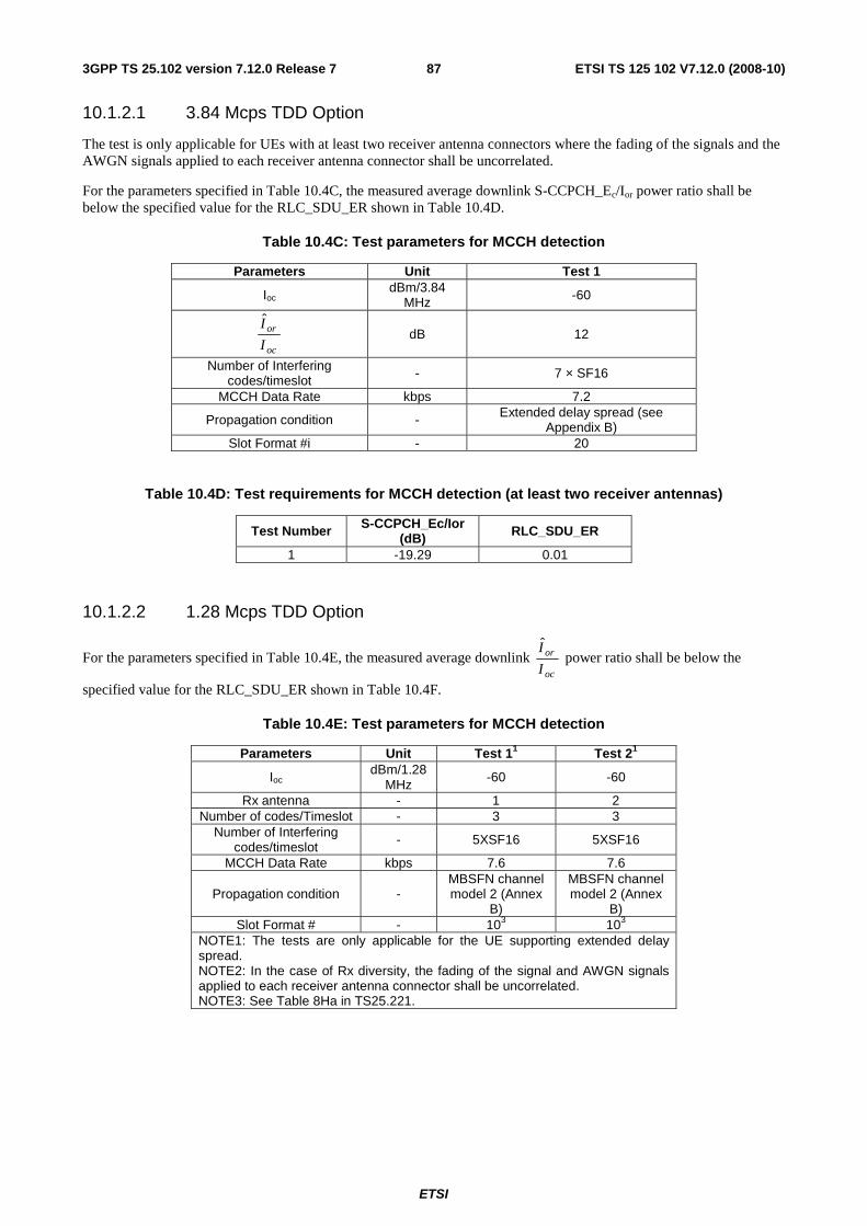
ETSI
ETSI TS 125 102 V7.12.0 (2008-10) 873GPP TS 25.102 version 7.12.0 Release 7
10.1.2.1 3.84 Mcps TDD Option
The test is only applicable for UEs with at least two receiver antenna connectors where the fading of the signals and the AWGN signals applied to each receiver antenna connector shall be uncorrelated.
For the parameters specified in Table 10.4C, the measured average downlink S-CCPCH_Ec/Ior power ratio shall be below the specified value for the RLC_SDU_ER shown in Table 10.4D.
Table 10.4C: Test parameters for MCCH detection
Parameters Unit Test 1
Ioc dBm/3.84
MHz -60
oc
or
I
I dB 12
Number of Interfering codes/timeslot - 7 × SF16
MCCH Data Rate kbps 7.2
Propagation condition - Extended delay spread (see Appendix B)
Slot Format #i - 20
Table 10.4D: Test requirements for MCCH detection (at least two receiver antennas)
Test Number S-CCPCH_Ec/Ior (dB) RLC_SDU_ER
1 -19.29 0.01
10.1.2.2 1.28 Mcps TDD Option
For the parameters specified in Table 10.4E, the measured average downlink oc
or
I
I power ratio shall be below the
specified value for the RLC_SDU_ER shown in Table 10.4F.
Table 10.4E: Test parameters for MCCH detection
Parameters Unit Test 11 Test 21
Ioc dBm/1.28
MHz -60 -60
Rx antenna - 1 2 Number of codes/Timeslot - 3 3
Number of Interfering codes/timeslot - 5XSF16 5XSF16
MCCH Data Rate kbps 7.6 7.6
Propagation condition - MBSFN channel model 2 (Annex
B)
MBSFN channel model 2 (Annex
B) Slot Format # - 103 103
NOTE1: The tests are only applicable for the UE supporting extended delay spread. NOTE2: In the case of Rx diversity, the fading of the signal and AWGN signals applied to each receiver antenna connector shall be uncorrelated. NOTE3: See Table 8Ha in TS25.221.
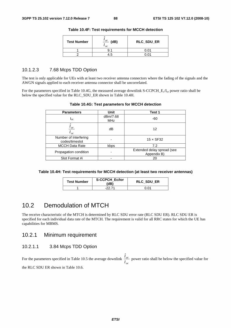
ETSI
ETSI TS 125 102 V7.12.0 (2008-10) 883GPP TS 25.102 version 7.12.0 Release 7
Table 10.4F: Test requirements for MCCH detection
Test Number oc
or
I
I (dB) RLC_SDU_ER
1 9.1 0.01 2 4.5 0.01
10.1.2.3 7.68 Mcps TDD Option
The test is only applicable for UEs with at least two receiver antenna connectors where the fading of the signals and the AWGN signals applied to each receiver antenna connector shall be uncorrelated.
For the parameters specified in Table 10.4G, the measured average downlink S-CCPCH_Ec/Ior power ratio shall be below the specified value for the RLC_SDU_ER shown in Table 10.4H.
Table 10.4G: Test parameters for MCCH detection
Parameters Unit Test 1
Ioc dBm/7.68
MHz -60
oc
or
I
I dB 12
Number of Interfering codes/timeslot - 15 × SF32
MCCH Data Rate kbps 7.2
Propagation condition - Extended delay spread (see Appendix B)
Slot Format #i - 20
Table 10.4H: Test requirements for MCCH detection (at least two receiver antennas)
Test Number S-CCPCH_Ec/Ior (dB) RLC_SDU_ER
1 -22.71 0.01
10.2 Demodulation of MTCH The receive characteristic of the MTCH is determined by RLC SDU error rate (RLC SDU ER). RLC SDU ER is specified for each individual data rate of the MTCH. The requirement is valid for all RRC states for which the UE has capabilities for MBMS.
10.2.1 Minimum requirement
10.2.1.1 3.84 Mcps TDD Option
For the parameters specified in Table 10.5 the average downlink oc
or
I
I
power ratio shall be below the specified value for
the RLC SDU ER shown in Table 10.6.

ETSI
ETSI TS 125 102 V7.12.0 (2008-10) 893GPP TS 25.102 version 7.12.0 Release 7
Table 10.5: Parameters for MTCH detection
Parameters Unit Test 1 Test 2 ∑(S-CCPCH_Ec)/Ior per active timeslot dB 0 0 ∑(S-CCPCH_Ec)/Ior per active timeslot dB 0 0
MTCH Data Rate kbps 128 256 Propagation condition - VA3 Number of Radio Links - 2 3
Table 10.6: Test requirements for MTCH detection
Test Number oc
or
I
I (dB) RLC SDU ER
1 5.7 0.1 2 5.5 0.1
10.2.1.2 1.28 Mcps TDD Option
For the parameters specified in Table 10.7 the average downlink oc
or
I
I
power ratio shall be below the specified value for
the RLC SDU ER shown in Table 10.8.
Table 10.7: Parameters for MTCH detection
Parameters Unit Test 1 Test 2
Ioc dBm/1.28
MHz -60
MTCH Data Rate kbps 64 128 Number of codes per timeslot - 8xSF16 14xSF16 Number of interfering codes
per timeslot - 0 0
Propagation condition - VA3 Number of Radio Links - 3 3
Table 10.8: Test requirements for MTCH detection
Test Number oc
or
I
I (dB) RLC SDU ER
1 4.8 0.1 2 6.0 0.1
10.2.1.3 7.68 Mcps TDD Option
For the parameters specified in Table 10.9 the average downlink oc
or
I
I
power ratio shall be below the specified value for
the RLC SDU ER shown in Table 10.10.

ETSI
ETSI TS 125 102 V7.12.0 (2008-10) 903GPP TS 25.102 version 7.12.0 Release 7
Table 10.9: Parameters for MTCH detection
Parameters Unit Test 1 Test 2
Ioc dBm/7.68
MHz -60
∑(S-CCPCH_Ec)/Ior per active timeslot dB -3 -3 MTCH Data Rate Kbps 128 256
Number of interfering codes/timeslot - 16 × SF32 16 × SF32 Propagation condition - VA3 Number of Radio Links - 2 3
Table 10.10: Test requirements for MTCH detection
Test Number oc
or
I
I (dB) RLC SDU ER
1 6.1 0.1 2 5.0 0.1
10.2.2 MBSFN capable UE
This requirement is applicable for UEs that are capable of receiving MBSFN.
10.2.2.1 3.84 Mcps TDD Option
The test is only applicable for UEs with at least two receiver antenna connectors where the fading of the signals and the AWGN signals applied to each receiver antenna connector shall be uncorrelated.
For the parameters specified in Table 10.10A the average downlink power ratio shall be below the specified value for the RLC SDU ER shown in Table 10.10B.
Table 10.10A: Parameters for MTCH detection
Parameters Unit Test 1 Ioc dBm/3.84
MHz -60
∑(S-CCPCH_Ec)/Ior per active timeslot dB 0 MTCH Data Rate kbps 512
Propagation condition - Extended delay spread (see Appendix B)
Number of Radio Links - 1 S-CCPCH Modulation - 16QAM
Table 10.10B: Test requirements for MTCH detection (at least two receiver antennas)
Test Number oc
or
I
I (dB) RLC SDU ER
1 14.58 0.1
10.2.2.2 1.28 Mcps TDD Option
For the parameters specified in Table 10.10C the average downlink power ratio shall be below the specified value for the RLC SDU ER shown in Table 10.10D.
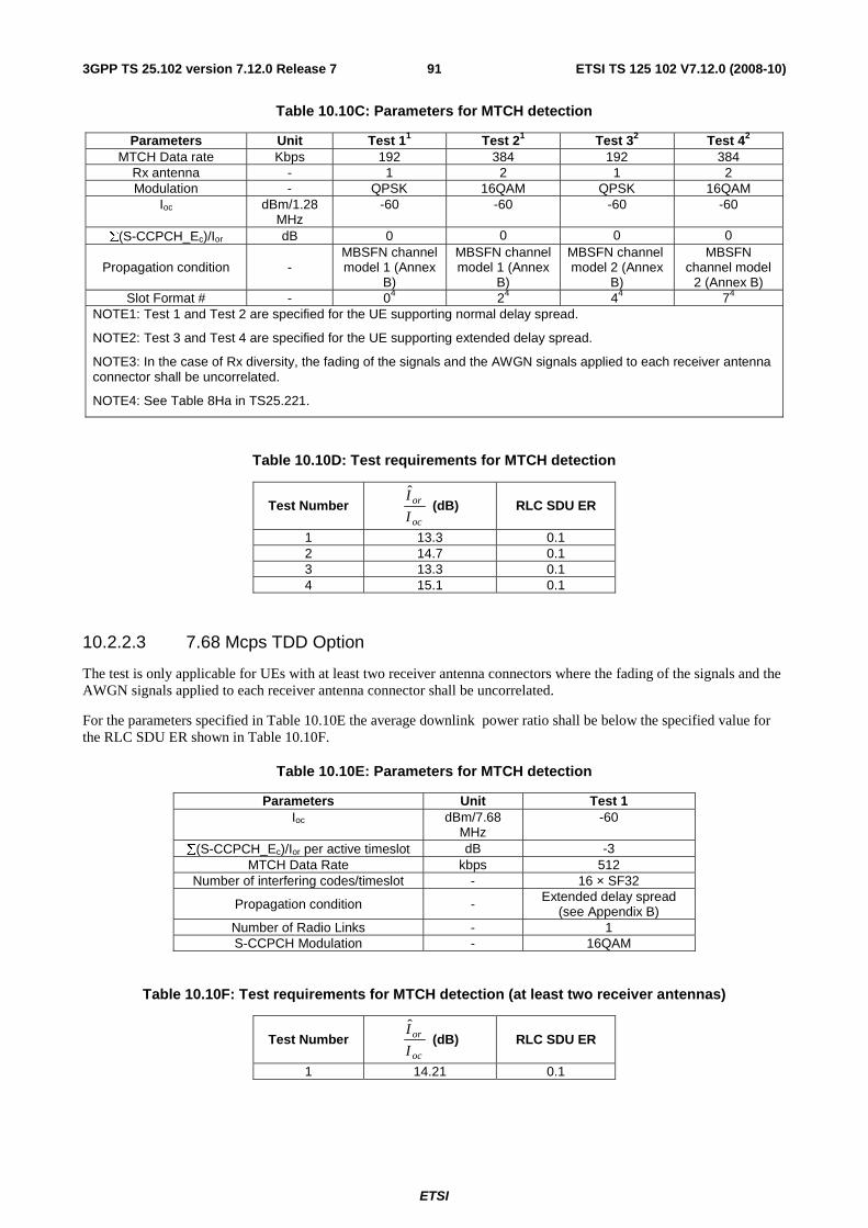
ETSI
ETSI TS 125 102 V7.12.0 (2008-10) 913GPP TS 25.102 version 7.12.0 Release 7
Table 10.10C: Parameters for MTCH detection
Parameters Unit Test 11 Test 21 Test 32 Test 42 MTCH Data rate Kbps 192 384 192 384
Rx antenna - 1 2 1 2 Modulation - QPSK 16QAM QPSK 16QAM
Ioc dBm/1.28 MHz
-60 -60 -60 -60
∑(S-CCPCH_Ec)/Ior dB 0 0 0 0
Propagation condition - MBSFN channel model 1 (Annex
B)
MBSFN channel model 1 (Annex
B)
MBSFN channel model 2 (Annex
B)
MBSFN channel model
2 (Annex B) Slot Format # - 04 24 44 74
NOTE1: Test 1 and Test 2 are specified for the UE supporting normal delay spread.
NOTE2: Test 3 and Test 4 are specified for the UE supporting extended delay spread.
NOTE3: In the case of Rx diversity, the fading of the signals and the AWGN signals applied to each receiver antenna connector shall be uncorrelated.
NOTE4: See Table 8Ha in TS25.221.
Table 10.10D: Test requirements for MTCH detection
Test Number oc
or
I
I (dB) RLC SDU ER
1 13.3 0.1 2 14.7 0.1 3 13.3 0.1 4 15.1 0.1
10.2.2.3 7.68 Mcps TDD Option
The test is only applicable for UEs with at least two receiver antenna connectors where the fading of the signals and the AWGN signals applied to each receiver antenna connector shall be uncorrelated.
For the parameters specified in Table 10.10E the average downlink power ratio shall be below the specified value for
the RLC SDU ER shown in Table 10.10F.
Table 10.10E: Parameters for MTCH detection
Parameters Unit Test 1 Ioc dBm/7.68
MHz -60
∑(S-CCPCH_Ec)/Ior per active timeslot dB -3 MTCH Data Rate kbps 512
Number of interfering codes/timeslot - 16 × SF32
Propagation condition - Extended delay spread (see Appendix B)
Number of Radio Links - 1 S-CCPCH Modulation - 16QAM
Table 10.10F: Test requirements for MTCH detection (at least two receiver antennas)
Test Number oc
or
I
I (dB) RLC SDU ER
1 14.21 0.1

ETSI
ETSI TS 125 102 V7.12.0 (2008-10) 923GPP TS 25.102 version 7.12.0 Release 7
10.2.3 MBSFN TDD & FDD same platform sharing
This test case is to ensure that a simulataneous demodulation of MTCH and FDD transmission is possible for a MBSFN TDD UE sharing the same platform with a FDD UE. The test is only applicable for TDD UEs with at least two receiver antenna connectors where the fading of the signals and the AWGN signals applied to each receiver antenna connector shall be uncorrelated.
10.2.3.1 3.84 Mcps TDD Option
For the parameters specified in Table 10.10G the average downlink Îor
power shall be below the specified value for the
RLC SDU ER shown in Table 10.10H.
Table 10.10G: Parameters for MTCH detection sharing same platform with FDD
Parameters Unit Test 1 Test 2 FDD UE Tx Pwr dBm/ 3.84 MHz Nominal Maximum Output
Power Nominal Maximum Output
Power Ioc dBm/ 3.84 MHz -infinity -infinity
∑(S-CCPCH_Ec)/Ior per active timeslot
dB 0 0
MTCH Data Rate kbps 512 512 Number of interfering
codes/timeslot - 0 0
Propagation condition - Extended Delay Spread (see Appendix B)
Extended Delay Spread (see Appendix B)
Number of Radio Links - 1 1 S-CCPCH Modulation - 16QAM 16QAM
TDD operating frequencies MHz 1900-1920 2570-2620
FDD operating band - Band I Band VII
TDD/FDD carrier frequencies -
Applicable for all combinations of TDD and FDD carrier frequencies except for combinations
where the carrier frequency separation is less than 15
MHz
Applicable for all combinations of TDD and FDD carrier frequencies except for combinations
where the carrier frequency separation is less than 15
MHz
Table 10.10H: Test requirements for MTCH detection sharing same platform with FDD (TDD UE has at least two receiver antennas)
Test Number Îor (dBm) RLC SDU ER 1 -83.42 0.1 2 -83.42 0.1
10.2.3.2 (void)
10.2.3.3 7.68 Mcps TDD Option
For the parameters specified in Table 10.10K the average downlink Îor
power shall be below the specified value for the
RLC SDU ER shown in Table 10.10L.
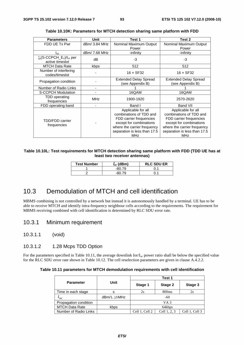
ETSI
ETSI TS 125 102 V7.12.0 (2008-10) 933GPP TS 25.102 version 7.12.0 Release 7
Table 10.10K: Parameters for MTCH detection sharing same platform with FDD
Parameters Unit Test 1 Test 2 FDD UE Tx Pwr dBm/ 3.84 MHz Nominal Maximum Output
Power Nominal Maximum Output
Power Ioc dBm/ 7.68 MHz -infinity -infinity
∑(S-CCPCH_Ec)/Ior per active timeslot
dB -3 -3
MTCH Data Rate kbps 512 512 Number of interfering
codes/timeslot - 16 × SF32 16 × SF32
Propagation condition - Extended Delay Spread (see Appendix B)
Extended Delay Spread (see Appendix B)
Number of Radio Links - 1 1 S-CCPCH Modulation - 16QAM 16QAM
TDD operating frequencies MHz 1900-1920 2570-2620
FDD operating band - Band I Band VII
TDD/FDD carrier frequencies -
Applicable for all combinations of TDD and FDD carrier frequencies except for combinations
where the carrier frequency separation is less than 17.5
MHz
Applicable for all combinations of TDD and FDD carrier frequencies except for combinations
where the carrier frequency separation is less than 17.5
MHz
Table 10.10L: Test requirements for MTCH detection sharing same platform with FDD (TDD UE has at least two receiver antennas)
Test Number Îor (dBm) RLC SDU ER 1 -80.79 0.1 2 -80.79 0.1
10.3 Demodulation of MTCH and cell identification MBMS combining is not controlled by a network but instead it is autonomously handled by a terminal. UE has to be able to receive MTCH and identify intra-frequency neighbour cells according to the requirements. The requirement for MBMS receiving combined with cell identification is determined by RLC SDU error rate.
10.3.1 Minimum requirement
10.3.1.1 (void)
10.3.1.2 1.28 Mcps TDD Option
For the parameters specified in Table 10.11, the average downlink Ior/Ioc power ratio shall be below the specified value for the RLC SDU error rate shown in Table 10.12. The cell reselection parameters are given in clause A.4.2.2.
Table 10.11 parameters for MTCH demodulation requirements with cell identification
Test 1 Parameter Unit
Stage 1 Stage 2 Stage 3
Time in each stage s 2s 800ms 2s
ocI dBm/1.28MHz -60
Propagation condition VA 3 MTCH Data Rate kbps 64kbps Number of Radio Links Cell 1, Cell 2 Cell 1, 2, 3 Cell 1, Cell 3

ETSI
ETSI TS 125 102 V7.12.0 (2008-10) 943GPP TS 25.102 version 7.12.0 Release 7
Table 10.12: Requirements for MTCH detection
Test Number oc
or
I
I RLC SDU ER
1 6.1 0.05
11 Performance requirement (E-DCH)
11.1 Detection of E-DCH HARQ ACK Indicator Channel (E-HICH)
The performance of the E-HICH detection is determined by the false ACK probability (probability of detecting an ACK given that a NACK was sent) and the false NACK probability (probability of detecting a NACK given that an ACK was sent).
11.1.1 Minimum requirement
11.1.1.1 3.84 Mcps TDD Option
For the parameters specified in Table 11.1 the average downlink E-HICH Ec/Ior power ratio shall be below the specified value for the false ACK and false NACK probabilities shown in Table 11.2.
Table 11.1: Test parameters for E-HICH detection (3.84 Mcps TDD option)
Parameters Unit Test 1 Test 2
Ioc dBm/3.84
MHz -60
oc
or
I
I dB 0
Number of Interfering codes/timeslot
- 7 × SF16 (all codes have equal powers)
E-HICH signalling pattern - 100% NACK 100% ACK Propagation condition - VA30
Table 11.2: Test requirements for E-HICH detection (3.84 Mcps TDD option)
Test Number E-HICH Ec/Ior (dB) Parameter Probability 1 -18.5 False ACK 2E-3 2 -18.5 False NACK 2E-2
11.1.1.2 1.28 Mcps TDD Option
For the parameters specified in Table 11.3 the average downlink E-HICH Ec/Ior power ratio shall be below the specified value for the false ACK and false NACK probabilities shown in Table 11.4.

ETSI
ETSI TS 125 102 V7.12.0 (2008-10) 953GPP TS 25.102 version 7.12.0 Release 7
Table 11.3: Test parameters for E-HICH detection (1.28 Mcps TDD option)
Parameters Unit Test 1 Test 2
Ioc dBm/1.28
MHz -60
oc
or
I
I dB 0
Number of Interfering codes/timeslot - 7 × SF16 (all codes have equal powers)
Midamble - Common midamble E-HICH signalling pattern - 100% NACK 100% ACK
Propagation condition - VA30
Table 11.4: Test requirements for E-HICH detection (1.28 Mcps TDD option)
Test Number E-HICH Ec/Ior (dB) Parameter Probability 1 -7.5 False ACK 2E-3 2 -7.5 False NACK 2E-2
11.1.1.3 7.68 Mcps TDD Option
For the parameters specified in Table 11.5 the average downlink E-HICH Ec/Ior power ratio shall be below the specified value for the false ACK and false NACK probabilities shown in Table 11.6.
Table 11.5: Test parameters for E-HICH detection (7.68 Mcps TDD option)
Parameters Unit Test 1 Test 2
Ioc dBm/7.68
MHz -60
oc
or
I
I dB 0
Number of Interfering codes/timeslot - 15 × SF32 (all codes have equal powers)
E-HICH signalling pattern - 100% NACK 100% ACK Propagation condition - VA30
Table 11.6: Test requirements for E-HICH detection (7.68 Mcps TDD option)
Test Number E-HICH Ec/Ior (dB) Parameter Probability 1 -21.7 False ACK 2E-3 2 -21.7 False NACK 2E-2
11.2 Demodulation of E-DCH Absolute Grant Channel (E-AGCH) The performance of the E-AGCH detection is determined by the missed detection probability.
11.2.1 Minimum requirement
11.2.1.1 3.84 Mcps TDD Option
For the parameters specified in Table 11.7 the average downlink E-AGCH Îor/Ioc power ratio shall be below the specified value for the missed detection probability shown in Table 11.8.

ETSI
ETSI TS 125 102 V7.12.0 (2008-10) 963GPP TS 25.102 version 7.12.0 Release 7
Table 11.7: Test parameters for E-AGCH detection (3.84 Mcps TDD option)
Parameters Unit Test 1
Ioc dBm/3.84
MHz -60
or
c
I
E dB -6.02
Number of Interfering codes/timeslot
- 3 × SF16
Total bits in Timeslot Resource Related Information (TRRI) bits 6
Total bits in Resource Duration Indicator (RDI) bits 3
Total bits in E-AGCH bits 38 Propagation condition - VA30
Table 11.8: Test requirements for E-AGCH detection (3.84 Mcps TDD option)
Test Number E-AGCH Îor/Ioc (dB) Missed Detection Probability
1 1.6 0.01
11.2.1.2 1.28 Mcps TDD Option
For the parameters specified in Table 11.9 the average downlink E-AGCH Îor/Ioc power ratio shall be below the specified value for the missed detection probability shown in Table 11.10.
Table 11.9: Test parameters for E-AGCH detection (1.28 Mcps TDD option)
Parameters Unit Test 1
Ioc dBm/1.28
MHz -60
or
c
I
E dB -3
Number of Interfering codes/timeslot - 2 × SF16
Total bits in Timeslot Resource Related Information (TRRI)
bits 5
Total bits in Resource Duration Indicator (RDI) bits 3
Total bits in E-AGCH bits 26 Midamble - Common midamble
Propagation condition - VA30
Table 11.10: Test requirements for E-AGCH detection (1.28 Mcps TDD option)
Test Number E-AGCH Îor/Ioc (dB) Missed Detection Probability
1 8 0.01
11.2.1.3 7.68 Mcps TDD Option
For the parameters specified in Table 11.11 the average downlink E-AGCH Îor/Ioc power ratio shall be below the specified value for the missed detection probability shown in Table 11.12.

ETSI
ETSI TS 125 102 V7.12.0 (2008-10) 973GPP TS 25.102 version 7.12.0 Release 7
Table 11.11: Test parameters for E-AGCH detection (7.68 Mcps TDD option)
Parameters Unit Test 1
Ioc dBm/7.68
MHz -60
or
c
I
E dB -9.03
Number of Interfering codes/timeslot
- 7 × SF32
Total bits in Timeslot Resource Related Information (TRRI) bits 6
Total bits in Resource Duration Indicator (RDI) bits 3
Total bits in E-AGCH bits 39 Propagation condition - VA30
Table 11.12: Test requirements for E-AGCH detection (7.68 Mcps TDD option)
Test Number E-AGCH Îor/Ioc (dB) Missed Detection Probability
1 1.2 0.01
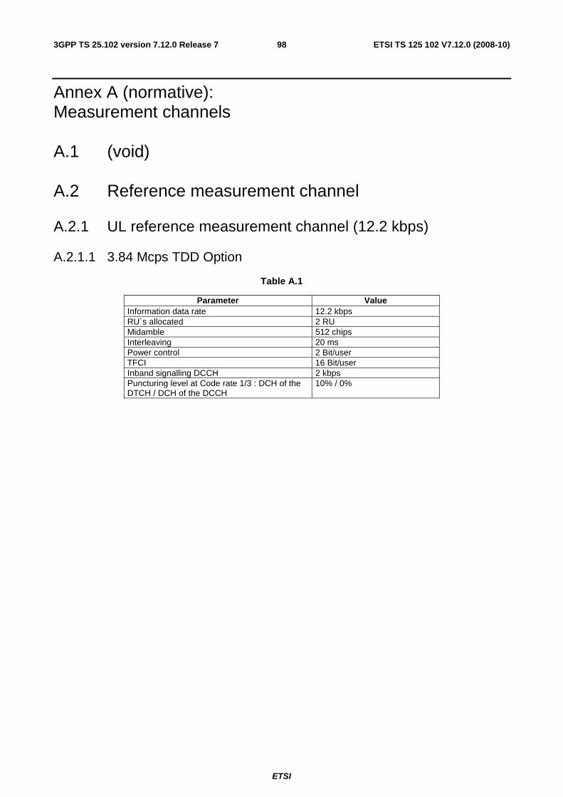
ETSI
ETSI TS 125 102 V7.12.0 (2008-10) 983GPP TS 25.102 version 7.12.0 Release 7
Annex A (normative): Measurement channels
A.1 (void)
A.2 Reference measurement channel
A.2.1 UL reference measurement channel (12.2 kbps)
A.2.1.1 3.84 Mcps TDD Option
Table A.1
Parameter Value Information data rate 12.2 kbps RU´s allocated 2 RU Midamble 512 chips Interleaving 20 ms Power control 2 Bit/user TFCI 16 Bit/user Inband signalling DCCH 2 kbps Puncturing level at Code rate 1/3 : DCH of the DTCH / DCH of the DCCH
10% / 0%

ETSI
ETSI TS 125 102 V7.12.0 (2008-10) 993GPP TS 25.102 version 7.12.0 Release 7
Information data 244
244CRC attachment
Tail bit attachment
[(260 +8)]x 3= 804
8
Conv. Coding 1/3
1st Interleaving
260 bit/20ms
804 bit/20ms
PuncturingRatemaching
402 bit punct. to 362 bitpuncturing-level: 10%
2 RU→244x2 = 488 Bits available
gross 488 bit -TFCI -TPC
-16 bit * 2-2 bit * 2
-Signal. -90 bitpunc. to 362 bit
SF=8 228 224TFCI
TFCI
TPC
8 82512chips
Service Multiplex.
2nd Interleaving
24416 16
244
402 bit punct. to 362 bitpuncturing-level: 10%
2 RU→244x2 = 488 Bits available
gross 488 bit -TFCI -TPC
-16 bit * 2-2 bit * 2
-Signal. -90 bitpunc. to 362 bit
964
100 12
8 Tail
CRC
MAC-Header
112
120 x 3= 360
Conv. Coding 1/3
362 362 362 362
TFCI
16
TPC
2
DCCH
362 362 362 362 90 90 90 90
90 90 90 90
452 452 452
Slot segmentation
452
452 TFCI
16
TPC
2
452 TFCI
16
TPC
2
452 TFCI
16
TPC
2
452TFCI / TPC
Repetition 0%Rate Matching (360)
228 224TFCI
TFCI
TPC
8 82512chips
228 224TFCI
TFCI
TPC
8 82512chips
228 224TFCI
TFCI
TPC
8 82512chips
Radio Frame #1 Radio Frame #2 Radio Frame #3 Radio Frame #4
MA MA MAMA
1st Interleaving (360)
[(260 +8)]x 3= 804
8260 bit/20ms
804 bit/20ms
RF-segmentation 402 402 402 402
Figure A.1
A.2.1.2 1.28 Mcps TDD Option
Table A.1A
Parameter Value Information data rate 12.2 kbps RU´s allocated 1TS (1*SF8) = 2RU/5ms Midamble 144 Interleaving 20 ms Power control 4 Bit/user/10ms TFCI 16 Bit/user/10ms 4 Bit reserved for future use (place of SS) 4 Bit/user/10ms Inband signalling DCCH 2.4 kbps Puncturing level at Code rate 1/3 : DCH of the DTCH / DCH of the DCCH
33% / 33%

ETSI
ETSI TS 125 102 V7.12.0 (2008-10) 1003GPP TS 25.102 version 7.12.0 Release 7
244
244 16
260bit/20ms 8
(260+8)*3=804
804bit/20ms
402 402
268 268
268 26860 60
328 328
176
328 16 8 328 16 8
176 176 176
Information Data
CRC attachement
Tail bit attachement
Conv. Coding 1/3
1st Interleaving
RF-Segmentation
Rate Matching
Service Multiplexing
2st Interleaving
TFCI, TPC and SS
Physical Channel Mapping
402 bit puncturing to 268 bitPuncturing Level: 33%
4 RU = 88 * 4 = 352 Bits available
gross
- TFCI- TPC- Reserved
- Signalling
puncturing to
352 bit
- 16 bit- 4 bit- 4 bit
- 60 bit
268 bit
4
100 12
112 8
(112+8)*3=360
360bit
60
Puncturing Level: 33%Rate Matching (240)
96
60 6060
328 16 8 328 16 8
176 176 176
402 bit puncturing to 268 bitPuncturing Level: 33%
4 RU = 88 * 4 = 352 Bits available
gross
- TFCI- TPC- Reserved
- Signalling
puncturing to
352 bit
- 16 bit- 4 bit- 4 bit
- 60 bit
268 bit
80484 4144
chips 4 80484 4144
chips 4 80484 4144
chips 4 80484 4144
chips 4Slot segmentation
Sub Frame #1 Sub Frame #2 Sub Frame #3 Sub Frame #4 Sub Frame #5 Sub Frame #6 Sub Frame #7 Sub Frame #8
DCCH
TFCITPC &Reserved
TFCI
80
MAC-Header
484 4144
chips 4SF=8 80484 4144
chips 4 80484 4144
chips 4 80484 4144
chips 4
244
244 16
260bit/20ms 8
(260+8)*3=804
804bit/20ms
402 402
268 268
268 26860 60
328 328
176
Figure A.1A

ETSI
ETSI TS 125 102 V7.12.0 (2008-10) 1013GPP TS 25.102 version 7.12.0 Release 7
A.2.1.3 7.68 Mcps TDD Option
Table A.1B
Parameter Value Information data rate 12.2 kbps RU´s allocated 2 RU Midamble 1024 chips Interleaving 20 ms Power control 2 Bit/user TFCI 16 Bit/user Inband signalling DCCH 2 kbps Puncturing level at Code rate 1/3 : DCH of the DTCH / DCH of the DCCH
10% / 0%
Information data 244
244CRC attachment
Tail bit attachment
[(260 +8)]x 3= 804
8
Conv. Coding 1/3
1 st Interleaving
260 bit/20ms
804 bit/20ms
PuncturingRatemaching
402 bit punct. to 362 bitpuncturing-level: 10%
2 RU→ 244x2 = 488 Bits available
gross 488 bit -TFCI -TPC
-16 bit * 2-2 bit * 2
-Signal. -90 bitpunc. to 362 bit
SF=16 228 224 TF CI TF
CI TPC
8 82 1024chips
Service Multiplex.
2nd Interleaving
24416 16
244
402 bit punct. to 362 bitpuncturing-level: 10%
2 RU → 244x2 = 488 Bits available
gross 488 bit -TFCI -TPC
-16 bit * 2-2 bit * 2
-Signal. -90 bitpunc. to 362 bit
964
100 12
8 Tail
CRC
MAC-Header
112
120 x 3= 360 Conv. Coding 1/3
362 362 362 362
TF CI 16
TPC 2
DCCH
362 362 362 362 90 90 90 90
90 90 90 90
452 452 452
Slot segmentation
452
452 TFCI 16
TPC 2
452 TF CI 16
TPC
2
452 TF CI 16
TPC 2
452TFCI / TPC
Repetition 0% Rate Matching (360)
228 224TF CI TF
CI TPC
8 82 1024 chips
228 224TF CI TF
CI TPC
8 82 1024chips
228 224 TF CI TF
CI TPC
8 82 1024chips
Radio Frame #1 Radio Frame #2 Radio Frame #3 Radio Frame #4
MA MA MA MA
1 st Interleaving (360)
[(260 +8)]x 3= 804
8 260 bit/20ms
804 bit/20ms
RF-segmentation 402 402 402 402
Figure A.1B
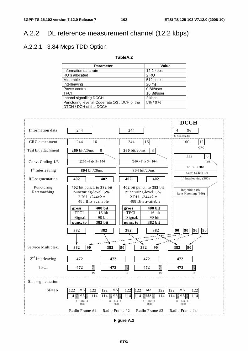
ETSI
ETSI TS 125 102 V7.12.0 (2008-10) 1023GPP TS 25.102 version 7.12.0 Release 7
A.2.2 DL reference measurement channel (12.2 kbps)
A.2.2.1 3.84 Mcps TDD Option
TableA.2
Parameter Value Information data rate 12.2 kbps RU´s allocated 2 RU Midamble 512 chips Interleaving 20 ms Power control 0 Bit/user TFCI 16 Bit/user Inband signalling DCCH 2 kbps Puncturing level at Code rate 1/3 : DCH of the DTCH / DCH of the DCCH
5% / 0 %
Information data 244
244CRC attachment
Tail bit attachment
[(260 +8)]x 3= 804
8
Conv. Coding 1/3
1st Interleaving
260 bit/20ms
804 bit/20ms
PuncturingRatemaching
402 bit punct. to 382 bitpuncturing-level: 5%
2 RU→244x2 = 488 Bits available
gross 488 bit -TFCI - 16 bit -Signal. -90 bitpunc. to 382 bit
SF=16
114 114TFCI
TFCI
8 8512chips
Service Multiplex.
2nd Interleaving
24416 16
244 964
100 12
8 Tail
CRC
MAC-Header
112
120 x 3= 360
Conv. Coding 1/3
382 382 382 382
TFCI
16
DCCH
382 382 382 382 90 90 90 90
90 90 90 90
472 472 472
Slot segmentation
472
472 TFCI
16
472 TFCI
16
472 TFCI
16
472TFCI
Repetition 0%Rate Matching (360)
114 114TFCI
TFCI
8 8512chips
114 114TFCI
TFCI
8 8512chips
114 114TFCI
TFCI
8 8512chips
Radio Frame #1 Radio Frame #2 Radio Frame #3 Radio Frame #4
MA MA MAMA
1st Interleaving (360)
[(260 +8)]x 3= 804
8260 bit/20ms
804 bit/20ms
122 122 122 122 122 122 122 122MA MA MAMA
RF-segmentation 402 402 402 402
402 bit punct. to 382 bitpuncturing-level: 5%
2 RU→244x2 = 488 Bits available
gross 488 bit -TFCI - 16 bit -Signal. -90 bitpunc. to 382 bit
Figure A.2
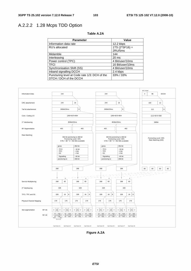
ETSI
ETSI TS 125 102 V7.12.0 (2008-10) 1033GPP TS 25.102 version 7.12.0 Release 7
A.2.2.2 1.28 Mcps TDD Option
Table A.2A
Parameter Value Information data rate 12.2 kbps RU's allocated 1TS (2*SF16) =
2RU/5ms Midamble 144 Interleaving 20 ms Power control (TPC) 4 Bit/user/10ms TFCI 16 Bit/user/10ms Synchronisation Shift (SS) 4 Bit/user/10ms Inband signalling DCCH 2.4 kbps Puncturing level at Code rate 1/3: DCH of the DTCH / DCH of the DCCH
33% / 33%
244
244 16
260bit/20ms 8
(260+8)*3=804
804bit/20ms
402 402
268 268
268 26860 60
328 328
176
328 16 8 328 16 8
176 176 176
Information Data
CRC attachement
Tail bit attachement
Conv. Coding 1/3
1st Interleaving
RF-Segmentation
Rate Matching
Service Multiplexing
2st Interleaving
TFCI, TPC and SS
Physical Channel Mapping
402 bit puncturing to 268 bitPuncturing Level: 33%
4 RU = 88 * 4 = 352 Bits available
gross
- TFCI- TPC- SS
- Signalling
puncturing to
352 bit
- 16 bit- 4 bit- 4 bit
- 60 bit
268 bit
4
100 12
112 8
(112+8)*3=360
360bit
60
Puncturing Level: 33%Rate Matching (240)
96
60 6060
Slot segmentation SF=16
Sub Frame #1 Sub Frame #2 Sub Frame #3 Sub Frame #4 Sub Frame #5 Sub Frame #6 Sub Frame #7 Sub Frame #8
DCCH
TFCITPC & SS
TFCI
36
MAC-Header
440 4144
chips4
44 144chips
44
SF=16 36440 4144
chips4
44 144chips
44
36440 4144
chips4
44 144chips
44
36440 4144
chips4
44 144chips
44
244
244 16
260bit/20ms 8
(260+8)*3=804
804bit/20ms
402 402
268 268
268 26860 60
328 328
176
328 16 8 328 16 8
176 176 176
402 bit puncturing to 268 bitPuncturing Level: 33%
4 RU = 88 * 4 = 352 Bits available
gross
- TFCI- TPC- SS
- Signalling
puncturing to
352 bit
- 16 bit- 4 bit- 4 bit
- 60 bit
268 bit
36440 4144
chips4
44 144chips
44
36440 4144
chips4
44 144chips
44
36440 4144
chips4
44 144chips
44
36440 4144
chips4
44 144chips
44
Figure A.2A

ETSI
ETSI TS 125 102 V7.12.0 (2008-10) 1043GPP TS 25.102 version 7.12.0 Release 7
A.2.2.3 7.68 Mcps TDD Option
TableA.2B
Parameter Value Information data rate 12.2 kbps RU´s allocated 2 RU Midamble 1024 chips Interleaving 20 ms Power control 0 Bit/user TFCI 16 Bit/user Inband signalling DCCH 2 kbps Puncturing level at Code rate 1/3 : DCH of the DTCH / DCH of the DCCH
5% / 0 %
Information data 244
244CRC attachment
Tail bit attachment
[(260 +8)]x 3= 804
8
Conv. Coding 1/3
1st Interleaving
260 bit/20ms
804 bit/20ms
PuncturingRatemaching
402 bit punct. to 382 bitpuncturing-level: 5%
2 RU →244x2 = 488 Bits available
gross 488 bit -TFCI - 16 bit -Signal. -90 bitpunc. to 382 bit
SF=32
114 114TF CI
TFCI
8 8 1024 chips
Service Multiplex.
2 nd Interleaving
24416 16
244 964
100 12
8 Tail
CRC
MAC-Header
112
120 x 3= 360
Conv. Coding 1/3
382 382 382 382
TFCI 16
DCCH
382 382 382 382 90 90 90 90
90 90 90 90
472 472 472
Slot segmentation
472
472 TF CI 16
472 TFCI 16
472 TFCI 16
472TFCI
Repetition 0%Rate Matching (360)
114 114TFCI
TF CI
8 81024 chips
114 114TFCI TF
CI 8 81024
chips
114 114TFCI TF
CI 8 8 1024
chips
Radio Frame #1 Radio Frame #2 Radio Frame #3 Radio Frame #4
MA MA MA MA
1st Interleaving (360)
[(260 +8)]x 3= 804
8 260 bit/20ms
804 bit/20ms
122 122 122 122 122 122 122 122MA MA MA MA
RF-segmentation 402 402 402 402
402 bit punct. to 382 bitpuncturing-level: 5%
2 RU →244x2 = 488 Bits available
gross 488 bit -TFCI - 16 bit -Signal. -90 bitpunc. to 382 bit
Figure A.2B
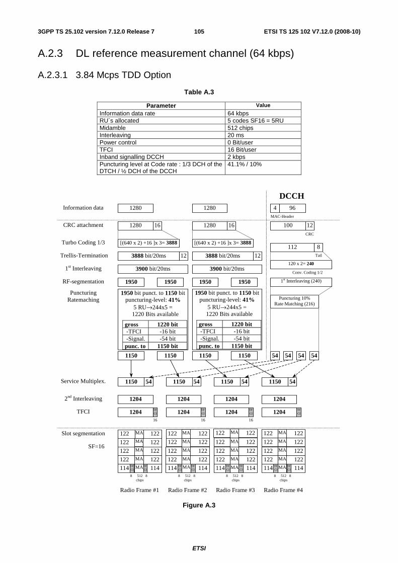
ETSI
ETSI TS 125 102 V7.12.0 (2008-10) 1053GPP TS 25.102 version 7.12.0 Release 7
A.2.3 DL reference measurement channel (64 kbps)
A.2.3.1 3.84 Mcps TDD Option
Table A.3
Parameter Value
Information data rate 64 kbps RU´s allocated 5 codes SF16 = 5RU Midamble 512 chips Interleaving 20 ms Power control 0 Bit/user TFCI 16 Bit/user Inband signalling DCCH 2 kbps Puncturing level at Code rate : 1/3 DCH of the DTCH / ½ DCH of the DCCH
41.1% / 10%
Information data 1280
1280CRC attachment
Turbo Coding 1/3 [(640 x 2) +16 ]x 3= 3888
12 Trellis-Termination
1st Interleaving
3888 bit/20ms
3900 bit/20ms
PuncturingRatemaching
1950 bit punct. to 1150 bitpuncturing-level: 41%
5 RU→244x5 = 1220 Bits available
gross 1220 bit -TFCI -16 bit -Signal. -54 bitpunc. to 1150 bit
SF=16
114 114TFCI
TFCI
8 8512chips
Service Multiplex.
2nd Interleaving
128016 16
1280
[(640 x 2) +16 ]x 3= 3888
3888 bit/20ms 12
3900 bit/20ms
964
100 12
8 Tail
CRC
MAC-Header
112
120 x 2= 240
Conv. Coding 1/2
1150 1150 1150 1150
TFCI
16
DCCH
1150 1150 1150 1150 54 54 54 54
54 54 54 54
1204 1204 1204
Slot segmentation
1204
1204 TFCI
16
1204 TFCI
16
1204 TFCI1204TFCI
Puncturing 10%Rate Matching (216)
114 114TFCI
TFCI
8 8512chips
114 114TFCI
TFCI
8 8512chips
114 114TFCI
TFCI
8 8512chips
Radio Frame #1 Radio Frame #2 Radio Frame #3 Radio Frame #4
MA MA MAMA
1st Interleaving (240)
122 122 122 122 122 122 122 122MA MA MAMA
122 122 122 122 122 122 122 122MA MA MAMA
122 122 122 122 122 122 122 122MA MA MAMA
122 122 122 122 122 122 122 122MA MA MAMA
RF-segmentation 1950 1950 1950 1950
1950 bit punct. to 1150 bitpuncturing-level: 41%
5 RU→244x5 = 1220 Bits available
gross 1220 bit -TFCI -16 bit -Signal. -54 bitpunc. to 1150 bit
Figure A.3
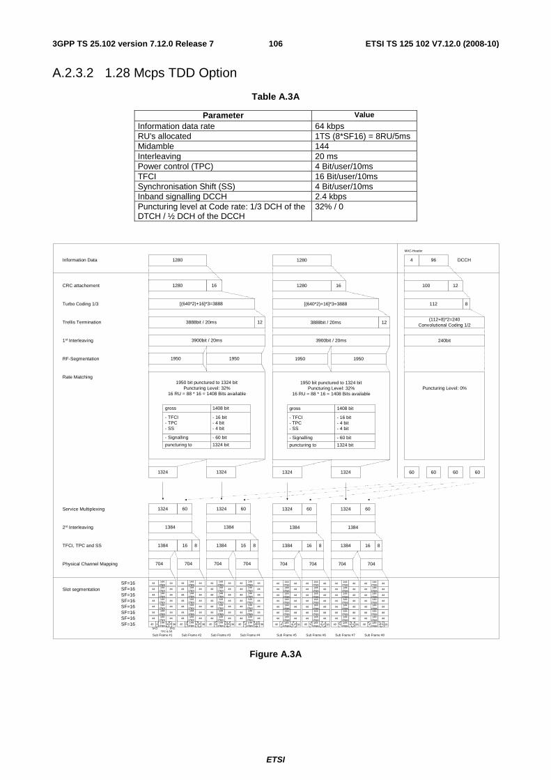
ETSI
ETSI TS 125 102 V7.12.0 (2008-10) 1063GPP TS 25.102 version 7.12.0 Release 7
A.2.3.2 1.28 Mcps TDD Option
Table A.3A
Parameter Value
Information data rate 64 kbps RU's allocated 1TS (8*SF16) = 8RU/5ms Midamble 144 Interleaving 20 ms Power control (TPC) 4 Bit/user/10ms TFCI 16 Bit/user/10ms Synchronisation Shift (SS) 4 Bit/user/10ms Inband signalling DCCH 2.4 kbps Puncturing level at Code rate: 1/3 DCH of the DTCH / ½ DCH of the DCCH
32% / 0
1280
1280 16
[(640*2)+16]*3=3888
3888bit / 20ms
3900bit / 20ms
1950 1950
1324 1324
1324 132460 60
1384 1384
704
1384 16 8 1384 16 8
704 704 704
Information Data
CRC attachement
Turbo Coding 1/3
Trellis Termination
1st Interleaving
RF-Segmentation
Rate Matching
Service Multiplexing
2st Interleaving
TFCI, TPC and SS
Physical Channel Mapping
1950 bit punctured to 1324 bitPuncturing Level: 32%
16 RU = 88 * 16 = 1408 Bits available
gross
- TFCI- TPC- SS
- Signalling
puncturing to
1408 bit
- 16 bit- 4 bit- 4 bit
- 60 bit
1324 bit
4
100 12
112 8
(112+8)*2=240Convolutional Coding 1/2
240bit
60
96
60 6060
Slot segmentationSF=16
Sub Frame #1 Sub Frame #2 Sub Frame #3 Sub Frame #4 Sub Frame #5 Sub Frame #6 Sub Frame #7 Sub Frame #8
DCCH
12
Puncturing Level: 0%
TFCITPC & SS
TFCI
MAC-Header
36440 4144
chips 4
44144
chips44
44144
chips44
44144
chips44
44144
chips44
44144
chips44
44144
chips44
44144
chips44
36440 4144
chips 4
44144
chips44
44144
chips44
44144
chips44
44144
chips44
44144
chips44
44144
chips44
44144
chips44
36440 4144
chips 4
44144
chips44
44144
chips44
44144
chips44
44144
chips44
44144
chips44
44144
chips44
44144
chips44
36440 4144
chips 4
44144
chips44
44144
chips44
44144
chips44
44144
chips44
44144
chips44
44144
chips44
44144
chips44
1280
1280 16
[(640*2)+16]*3=3888
3888bit / 20ms
3900bit / 20ms
1950 1950
1324 1324
1324 132460 60
1384 1384
704
1384 16 8 1384 16 8
704 704 704
1950 bit punctured to 1324 bitPuncturing Level: 32%
16 RU = 88 * 16 = 1408 Bits available
gross
- TFCI- TPC- SS
- Signalling
puncturing to
1408 bit
- 16 bit- 4 bit- 4 bit
- 60 bit
1324 bit
12
36440 4144
chips4
44144
chips 44
44144
chips44
44144
chips44
44144
chips44
44144
chips44
44144
chips44
44144
chips44
36440 4144
chips4
44144
chips 44
44144
chips44
44144
chips44
44144
chips44
44144
chips44
44144
chips44
44144
chips44
36440 4144
chips4
44144
chips 44
44144
chips44
44144
chips44
44144
chips44
44144
chips44
44144
chips44
44144
chips44
36440 4144
chips4
44144
chips 44
44144
chips44
44144
chips44
44144
chips44
44144
chips44
44144
chips44
44144
chips44
SF=16SF=16SF=16SF=16SF=16SF=16SF=16
Figure A.3A

ETSI
ETSI TS 125 102 V7.12.0 (2008-10) 1073GPP TS 25.102 version 7.12.0 Release 7
A.2.3.3 7.68 Mcps TDD Option
Table A.3B
Parameter Value
Information data rate 64 kbps RU´s allocated 5 codes SF32 = 5RU Midamble 1024 chips Interleaving 20 ms Power control 0 Bit/user TFCI 16 Bit/user Inband signalling DCCH 2 kbps Puncturing level at Code rate : 1/3 DCH of the DTCH / ½ DCH of the DCCH
41.1% / 10%
Information data 1280
1280 CRC attachment
Turbo Coding 1/3 [(640 x 2) +16 ]x 3= 3888
12 Trellis-Termination
1 st Interleaving
3888 bit/20ms
3900 bit/20ms
Puncturing Ratemaching
1950 bit punct. to 1150 bit puncturing-level: 41%
5 RU → 244x5 = 1220 Bits available
gross 1220 bit -TFCI -16 bit -Signal. -54 bit punc. to 1150 bit
SF=32
114 114 TF CI TF
CI 8 8 1024
chips
Service Multiplex.
2 nd Interleaving
1280 16 16
1280
[(640 x 2) +16 ]x 3= 3888
3888 bit/20ms 12
3900 bit/20ms
96 4
100 12
8 Tail
CRC
MAC-Header
112
120 x 2= 240 Conv. Coding 1/2
1150 1150 1150 1150
TF CI 16
DCCH
1150 1150 1150 1150 54 54 54 54
54 54 54 54
1204 1204 1204
Slot segmentation
1204
1204 TF CI 16
1204 TF CI 16
1204 TF CI 1204 TFCI
Puncturing 10% Rate Matching (216)
114 114 TF CI TF
CI 8 8 1024
chips 114 114 TF
CI TF CI
8 8 1024 chips
114 114 TF CI TF
CI 8 8 1024
chips Radio Frame #1 Radio Frame #2 Radio Frame #3 Radio Frame #4
MA MA MA MA
1 st Interleaving (240)
122 122 122 122 122 122 122 122 MA MA MA MA 122 122 122 122 122 122 122 122 MA MA MA MA
122 122 122 122 122 122 122 122 MA MA MA MA 122 122 122 122 122 122 122 122 MA MA MA MA
RF-segmentation 1950 1950 1950 1950 1950 bit punct. to 1150 bit
puncturing-level: 41% 5 RU → 244x5 =
1220 Bits available gross 1220 bit -TFCI -16 bit -Signal. -54 bit punc. to 1150 bit
Figure A.3B
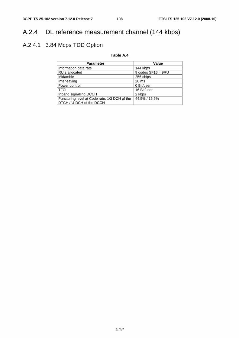
ETSI
ETSI TS 125 102 V7.12.0 (2008-10) 1083GPP TS 25.102 version 7.12.0 Release 7
A.2.4 DL reference measurement channel (144 kbps)
A.2.4.1 3.84 Mcps TDD Option
Table A.4
Parameter Value Information data rate 144 kbps RU´s allocated 9 codes SF16 = 9RU Midamble 256 chips Interleaving 20 ms Power control 0 Bit/user TFCI 16 Bit/user Inband signalling DCCH 2 kbps Puncturing level at Code rate: 1/3 DCH of the DTCH / ½ DCH of the DCCH
44.5% / 16.6%

ETSI
ETSI TS 125 102 V7.12.0 (2008-10) 1093GPP TS 25.102 version 7.12.0 Release 7
Information data 2880
2880CRC attachment
Turbo Coding 1/3 [(1440 x 2) +16 ] x 3= 8688
12 Trellis-Termination
1st Interleaving
8688 bit/20ms
8700 bit/20ms
PuncturingRatemaching
4350 bit punct. to 2418 bitpuncturing-level: 44%
9 RU→276x9 = 2484 Bits available
gross 2484 bit -TFCI - 16 bit -Signal. -50 bitpunc. to 2418 bit
SF=16
130 130TFCI
TFCI
8 8256chips
138 138
Service Multiplex.
2nd Interleaving
288016 16
2880
[(1440 x 2) +16 ] x 3=8688
8688 bit/20ms 12
8700 bit/20ms
4350 bit punct. to 2418 bitpuncturing-level: 44%
9 RU→276x9 = 2484 Bits available
gross 2484 bit -TFCI - 16 bit -Signal. -50 bitpunc. to 2418 bit
964
100 12
8 Tail
CRC
MAC-Header
112
120 x 2= 240
Conv. Coding 1/2
2418 2418 2418 2418
TFCI
16
DCCH
2418 2418 2418 2418 50 50 50 50
50 50 50 50
2468 2468 2468
Slot segmentation
2468
2468 TFCI
16
2468 TFCI
16
2468 TFCI
16
2468TFCI
Puncturing 17%Rate Matching (200)
130 130TFCI
TFCI
8 8256chips
138 138
130 130TFCI
TFCI
8 8256chips
138 138
130 130TFCI
TFCI
8 8256chips
138 138
Radio Frame #1 Radio Frame #2 Radio Frame #3 Radio Frame #4
MA
MA
MA
MA
MA
MA
MA
MA
1st Interleaving (240)
138 138 138 138 138 138 138 138MA MA MA MA
138 138 138 138 138 138 138 138MA MA MA MA
138 138 138 138 138 138 138 138MA MA MA MA
138 138 138 138 138 138 138 138MA MA MA MA
138 138 138 138 138 138 138 138MA MA MA MA
138 138 138 138 138 138 138 138MA MA MA MA
138 138 138 138 138 138 138 138MA MA MA MA
RF-segmentation 4350 4350 4350 4350
Figure A.4
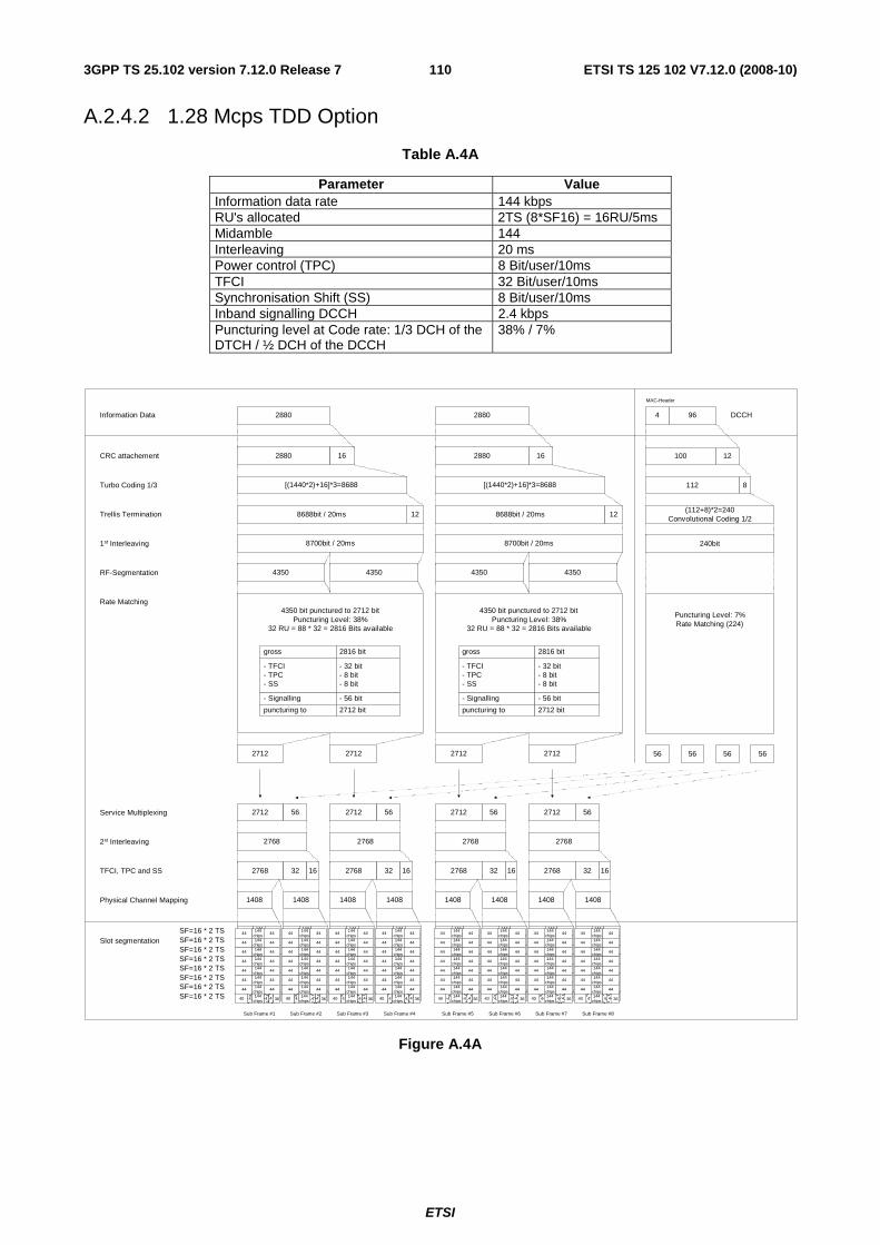
ETSI
ETSI TS 125 102 V7.12.0 (2008-10) 1103GPP TS 25.102 version 7.12.0 Release 7
A.2.4.2 1.28 Mcps TDD Option
Table A.4A
Parameter Value Information data rate 144 kbps RU's allocated 2TS (8*SF16) = 16RU/5ms Midamble 144 Interleaving 20 ms Power control (TPC) 8 Bit/user/10ms TFCI 32 Bit/user/10ms Synchronisation Shift (SS) 8 Bit/user/10ms Inband signalling DCCH 2.4 kbps Puncturing level at Code rate: 1/3 DCH of the DTCH / ½ DCH of the DCCH
38% / 7%
2880
2880 16
[(1440*2)+16]*3=8688
8688bit / 20ms
8700bit / 20ms
4350 4350
2712 2712
2712 271256 56
2768 2768
1408
2768 32 2768 32
1408 1408 1408
Information Data
CRC attachement
Turbo Coding 1/3
Trellis Termination
1st Interleaving
RF-Segmentation
Rate Matching
Service Multiplexing
2st Interleaving
TFCI, TPC and SS
Physical Channel Mapping
4350 bit punctured to 2712 bitPuncturing Level: 38%
32 RU = 88 * 32 = 2816 Bits available
gross
- TFCI- TPC- SS
- Signalling
puncturing to
2816 bit
- 32 bit- 8 bit- 8 bit
- 56 bit
2712 bit
4
100 12
112 8
(112+8)*2=240Convolutional Coding 1/2
240bit
56
96
56 5656
Slot segmentation
Sub Frame #1 Sub Frame #2 Sub Frame #3 Sub Frame #4 Sub Frame #5 Sub Frame #6 Sub Frame #7 Sub Frame #8
DCCH
12
Puncturing Level: 7%Rate Matching (224)
16 16
MAC-Header
36440 4144
chips 4
44144
chips44
44144
chips44
44144
chips44
44144
chips44
44144
chips44
44144
chips44
44144
chips44
36440 4144
chips4
44144
chips44
44144
chips 44
44 144chips
44
44144
chips44
44144
chips44
44144
chips44
44144
chips44
36440 4144
chips 4
44144
chips44
44144
chips44
44144
chips44
44144
chips44
44144
chips44
44144
chips44
44144
chips44
36440 4144
chips4
44144
chips44
44144
chips 44
44 144chips
44
44144
chips44
44144
chips44
44144
chips44
44144
chips44
36440 4144
chips 4
44144
chips44
44144
chips44
44144
chips44
44144
chips44
44144
chips44
44144
chips44
44144
chips44
36440 4144
chips4
44144
chips44
44144
chips 44
44 144chips
44
44144
chips44
44144
chips44
44144
chips44
44144
chips44
36440 4144
chips 4
44144
chips44
44144
chips44
44144
chips44
44144
chips44
44144
chips44
44144
chips44
44144
chips44
36440 4144
chips4
44144
chips44
44144
chips 44
44 144chips
44
44144
chips44
44144
chips44
44144
chips44
44144
chips44
SF=16 * 2 TSSF=16 * 2 TSSF=16 * 2 TSSF=16 * 2 TSSF=16 * 2 TSSF=16 * 2 TSSF=16 * 2 TSSF=16 * 2 TS
2880
2880 16
[(1440*2)+16]*3=8688
8688bit / 20ms
8700bit / 20ms
4350 4350
2712 2712
2712 271256 56
2768 2768
1408
2768 32 2768 32
1408 1408 1408
4350 bit punctured to 2712 bitPuncturing Level: 38%
32 RU = 88 * 32 = 2816 Bits available
gross
- TFCI- TPC- SS
- Signalling
puncturing to
2816 bit
- 32 bit- 8 bit- 8 bit
- 56 bit
2712 bit
12
16 16
36440 4144
chips 4
44144
chips44
44144
chips44
44144
chips44
44144
chips44
44144
chips44
44144
chips44
44144
chips44
36440 4144
chips4
44144
chips44
44144
chips 44
44 144chips
44
44144
chips44
44144
chips44
44144
chips44
44144
chips44
36440 4144
chips 4
44144
chips44
44144
chips44
44144
chips44
44144
chips44
44144
chips44
44144
chips44
44144
chips44
36440 4144
chips4
44144
chips44
44144
chips 44
44 144chips
44
44144
chips44
44144
chips44
44144
chips44
44144
chips44
36440 4144
chips 4
44144
chips44
44144
chips44
44144
chips44
44144
chips44
44144
chips44
44144
chips44
44144
chips44
36440 4144
chips4
44144
chips44
44144
chips 44
44 144chips
44
44144
chips44
44144
chips44
44144
chips44
44144
chips44
36440 4144
chips 4
44144
chips44
44144
chips44
44144
chips44
44144
chips44
44144
chips44
44144
chips44
44144
chips44
36440 4144
chips4
44144
chips44
44144
chips 44
44 144chips
44
44144
chips44
44144
chips44
44144
chips44
44144
chips44
Figure A.4A

ETSI
ETSI TS 125 102 V7.12.0 (2008-10) 1113GPP TS 25.102 version 7.12.0 Release 7
A.2.4.3 7.68 Mcps TDD Option
Table A.4B
Parameter Value Information data rate 144 kbps RU´s allocated 9 codes SF32 = 9RU Midamble 512 chips Interleaving 20 ms Power control 0 Bit/user TFCI 16 Bit/user Inband signalling DCCH 2 kbps Puncturing level at Code rate: 1/3 DCH of the DTCH / ½ DCH of the DCCH
44.5% / 16.6%

ETSI
ETSI TS 125 102 V7.12.0 (2008-10) 1123GPP TS 25.102 version 7.12.0 Release 7
Information data 2880
2880 CRC attachment
Turbo Coding 1/3 [(1440 x 2) +16 ] x 3= 8688
12 Trellis-Termination
1 st Interleaving
8688 bit/20ms
8700 bit/20ms
Puncturing Ratemaching
SF=32
130 130 TF CI TF
CI 8 8 512
chips
138 138
Service Multiplex.
2 nd
Interleaving
2880 16 16
2880
[(1440 x 2) +16 ] x 3= 8688
8688 bit/20ms 12
8700 bit/20ms
96 4
100 12
8 Tail
CRC
MAC-Header
112
120 x 2= 240 Conv. Coding 1/2
2418 2418 2418 2418
TF CI 16
DCCH
2418 2418 2418 2418 50 50 50 50
50 50 50 50
2468 2468 2468
Slot segmentation
2468
2468 TF CI 16
2468 TF CI 16
2468 TF CI 16
2468 TFCI
Puncturing 17% Rate Matching (200)
130 130 TF CI TF
CI 8 8 512
chips
138 138
130 130 TF CI TF
CI 8 8 512
chips
138 138
130 130 TF CI TF
CI 8 8 512
chips
138 138
Radio Frame #1 Radio Frame #2 Radio Frame #3 Radio Frame #4
MA
MA
MA
MA
MA
MA
MA
MA
1 st Interleaving (240)
138 138 138 138 138 138 138 138 MA MA MA MA
138 138 138 138 138 138 138 138 MA MA MA MA
138 138 138 138 138 138 138 138 MA MA MA MA
138 138 138 138 138 138 138 138 MA MA MA MA
138 138 138 138 138 138 138 138 MA MA MA MA
138 138 138 138 138 138 138 138 MA MA MA MA
138 138 138 138 138 138 138 138 MA MA MA MA
RF-segmentation 4350 4350 4350 4350
4350 bit punct to 2418 bit puncturing-level: 44%
9 RU → 276 × 9 = 2484 bits available
4350 bit punct to 2418 bit puncturing-level: 44%
9 RU → 276 × 9 = 2484 bits available
gross 2484 bit -TFCI -16 bit -Signal -50 bit punc to 2418 bit
gross 2484 bit -TFCI -16 bit -Signal -50 bit punc to 2418 bit
Figure A.4B

ETSI
ETSI TS 125 102 V7.12.0 (2008-10) 1133GPP TS 25.102 version 7.12.0 Release 7
A.2.5 DL reference measurement channel (384 kbps)
A.2.5.1 3.84 Mcps TDD Option
Table A.5
Parameter Value Information data rate 384 kbps RU´s allocated 8*3TS = 24RU Midamble 256 chips Interleaving 20 ms Power control 0 Bit/user TFCI 16 Bit/user Inband signalling DCCH 2 kbps Puncturing level at Code rate : 1/3 DCH of the DTCH / ½ DCH of the DCCH
43.4% / 15.3%
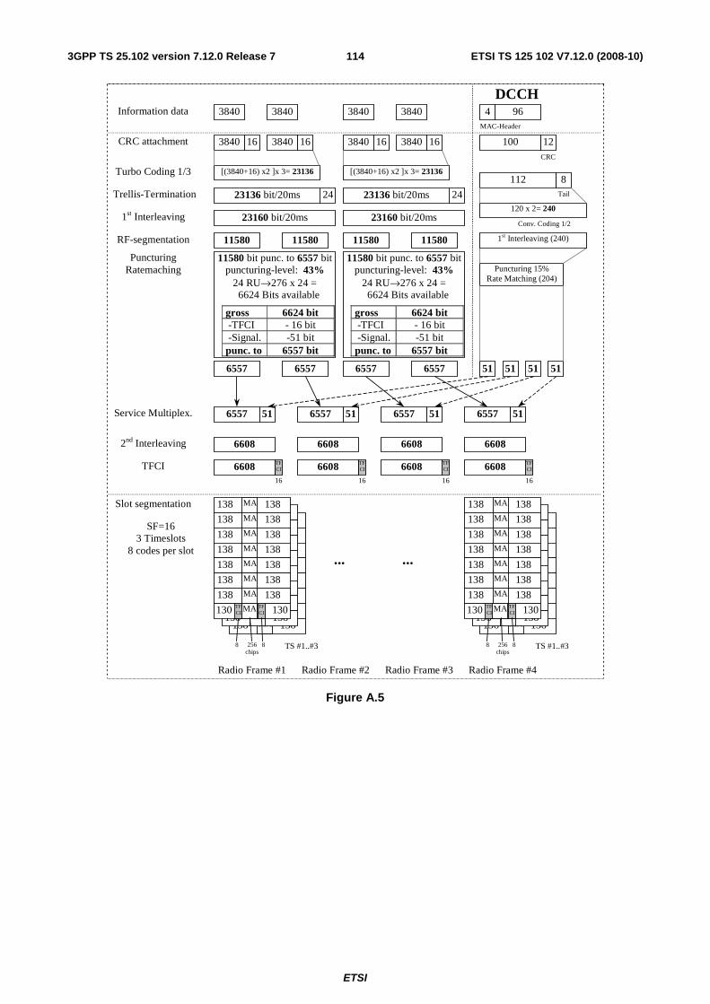
ETSI
ETSI TS 125 102 V7.12.0 (2008-10) 1143GPP TS 25.102 version 7.12.0 Release 7
Information data 3840
3840CRC attachment
Turbo Coding 1/3 [(3840+16) x2 ]x 3= 23136
24 Trellis-Termination
1st Interleaving
23136 bit/20ms
23160 bit/20ms
PuncturingRatemaching
11580 bit punc. to 6557 bitpuncturing-level: 43%
24 RU→276 x 24 = 6624 Bits available
gross 6624 bit -TFCI - 16 bit -Signal. -51 bitpunc. to 6557 bit
SF=163 Timeslots
8 codes per slot
Service Multiplex.
2nd Interleaving
16
964
100 12
8 Tail
CRC
MAC-Header
112
120 x 2= 240
Conv. Coding 1/2
6557 6557 6557 6557
TFCI
16
DCCH
6557 6557 6557 6557 51 51 51 51
51 51 51 51
6608 6608 6608
Slot segmentation
6608
6608 TFCI
16
6608 TFCI
16
6608 TFCI
16
6608TFCI
Puncturing 15%Rate Matching (204)
Radio Frame #1 Radio Frame #2 Radio Frame #3 Radio Frame #4
1st Interleaving (240)
TS #1..#3
... ...
138 138MA
138 138MA
138 138MA
138 138MA
138 138MA
138 138MA
138 138MA
138 138MA
138 138MA
138 138MA
138 138MA
138 138MA
138 138MA
138 138MA
138 138MA
138 138MA130 130TF
CITFCI
MA
138 138MA
138 138MA
138 138MA
138 138MA
138 138MA
138 138MA
138 138MA
8 8256chips
138 138MA
138 138MA
138 138MA
138 138MA
138 138MA
138 138MA
138 138MA
138 138MA
138 138MA
138 138MA
138 138MA
138 138MA
138 138MA
138 138MA
138 138MA
138 138MA130 130TF
CITFCI
MA
138 138MA
138 138MA
138 138MA
138 138MA
138 138MA
138 138MA
138 138MA
8 8256chips
TS #1..#3
RF-segmentation 11580 11580
3840
3840 16
3840
3840
[(3840+16) x2 ]x 3= 23136
2423136 bit/20ms
23160 bit/20ms
11580 bit punc. to 6557 bitpuncturing-level: 43%
24 RU→276 x 24 = 6624 Bits available
gross 6624 bit -TFCI - 16 bit -Signal. -51 bitpunc. to 6557 bit
16
11580 11580
3840
3840 16
Figure A.5

ETSI
ETSI TS 125 102 V7.12.0 (2008-10) 1153GPP TS 25.102 version 7.12.0 Release 7
A.2.5.2 1.28 Mcps TDD Option
Table A.5A
Parameter Value Information data rate 384 kbps RU's allocated 4TS (10*SF16) =
40RU/5ms Midamble 144 Interleaving 20 ms Power control (TPC) 16 Bit/user/10ms TFCI 64 Bit/user/10ms Synchronisation Shift (SS) 16 Bit/user/10ms Inband signalling DCCH max.2 kbps Puncturing level at Code rate: 1/3 DCH of the DTCH / ½ DCH of the DCCH
41% / 12%
3840
3840 16
[(3840+16)*2]*3=23136
23136bit / 20ms
23160bit / 20ms
11580 11580
6891 6891
6891 689153 53
6944 6944
3520
6944 64 6944 64
3520 3520 3520
Information Data
CRC attachement
Turbo Coding 1/3
Trellis Termination
1st Interleaving
RF-Segmentation
Rate Matching
Service Multiplexing
2st Interleaving
TFCI, TPC and SS
Physical Channel Mapping
11580 bit punctured to 6891 bitPuncturing Level: 41%
80 RU = 88 * 80 = 7040 Bits available
gross
- TFCI- TPC- SS
- Signalling
puncturing to
7040 bit
- 64 bit- 16 bit- 16 bit
53
6891 bit
16
96 16
112 8
(112+8)*2=240Convolutional Coding 1/2
240bit
53
max 80
53 5353
Slot segmentation
Sub Frame #1 Sub Frame #2 Sub Frame #3 Sub Frame #4 Sub Frame #5 Sub Frame #6 Sub Frame #7 Sub Frame #8
DCCH
24
Puncturing Level: 12%Rate Matching (212)
SF=16 * 4 TS
32 32
3840
3840 16
44 144c 44
36440 4 144c 4
44 144c 44
44 144c 44
44 144c 4444 144c 44
44 144c 44
44 144c 44
44 144c 44
44 144c 44
44 144c 44
36440 4 144c 4
44 144c 44
44 144c 44
44 144c 4444 144c 44
44 144c 44
44 144c 44
44 144c 44
44 144c 44
44 144c 44
36440 4 144c 4
44 144c 44
44 144c 44
44 144c 4444 144c 44
44 144c 44
44 144c 44
44 144c 44
44 144c 44
44 144c 44
36440 4 144c 4
44 144c 44
44 144c 44
44 144c 4444 144c 44
44 144c 44
44 144c 44
44 144c 44
44 144c 44
SF=16 * 4 TSSF=16 * 4 TSSF=16 * 4 TSSF=16 * 4 TSSF=16 * 4 TSSF=16 * 4 TSSF=16 * 4 TSSF=16 * 4 TSSF=16 * 4 TS
44 144c 44
36440 4 144c 4
44 144c 44
44 144c 44
44 144c 4444 144c 44
44 144c 44
44 144c 44
44 144c 44
44 144c 44
44 144c 44
36440 4 144c 4
44 144c 44
44 144c 44
44 144c 4444 144c 44
44 144c 44
44 144c 44
44 144c 44
44 144c 44
44 144c 44
36440 4 144c 4
44 144c 44
44 144c 44
44 144c 4444 144c 44
44 144c 44
44 144c 44
44 144c 44
44 144c 44
44 144c 44
36440 4 144c 4
44 144c 44
44 144c 44
44 144c 4444 144c 44
44 144c 44
44 144c 44
44 144c 44
44 144c 44
44 144c 44
36440 4 144c 4
44 144c 44
44 144c 44
44 144c 4444 144c 44
44 144c 44
44 144c 44
44 144c 44
44 144c 44
44 144c 44
36440 4 144c 4
44 144c 44
44 144c 44
44 144c 4444 144c 44
44 144c 44
44 144c 44
44 144c 44
44 144c 44
44 144c 44
36440 4 144c 4
44 144c 44
44 144c 44
44 144c 4444 144c 44
44 144c 44
44 144c 44
44 144c 44
44 144c 44
44 144c 44
36440 4 144c 4
44 144c 44
44 144c 44
44 144c 4444 144c 44
44 144c 44
44 144c 44
44 144c 44
44 144c 44
44 144c 44
36440 4 144c 4
44 144c 44
44 144c 44
44 144c 4444 144c 44
44 144c 44
44 144c 44
44 144c 44
44 144c 44
44 144c 44
36440 4 144c 4
44 144c 44
44 144c 44
44 144c 4444 144c 44
44 144c 44
44 144c 44
44 144c 44
44 144c 44
44 144c 44
36440 4 144c 4
44 144c 44
44 144c 44
44 144c 4444 144c 44
44 144c 44
44 144c 44
44 144c 44
44 144c 44
44 144c 44
36440 4 144c 4
44 144c 44
44 144c 44
44 144c 4444 144c 44
44 144c 44
44 144c 44
44 144c 44
44 144c 44
44 144c 44
36440 4 144c 4
44 144c 44
44 144c 44
44 144c 4444 144c 44
44 144c 44
44 144c 44
44 144c 44
44 144c 44
44 144c 44
36440 4 144c 4
44 144c 44
44 144c 44
44 144c 4444 144c 44
44 144c 44
44 144c 44
44 144c 44
44 144c 44
44 144c 44
36440 4 144c 4
44 144c 44
44 144c 44
44 144c 4444 144c 44
44 144c 44
44 144c 44
44 144c 44
44 144c 44
44 144c 44
36440 4 144c 4
44 144c 44
44 144c 44
44 144c 4444 144c 44
44 144c 44
44 144c 44
44 144c 44
44 144c 44
44 144c 44
36440 4 144c 4
44 144c 44
44 144c 44
44 144c 4444 144c 44
44 144c 44
44 144c 44
44 144c 44
44 144c 44
44 144c 44
36440 4 144c 4
44 144c 44
44 144c 44
44 144c 4444 144c 44
44 144c 44
44 144c 44
44 144c 44
44 144c 44
44 144c 44
36440 4 144c 4
44 144c 44
44 144c 44
44 144c 4444 144c 44
44 144c 44
44 144c 44
44 144c 44
44 144c 44
44 144c 44
36440 4 144c 4
44 144c 44
44 144c 44
44 144c 4444 144c 44
44 144c 44
44 144c 44
44 144c 44
44 144c 44
44 144c 44
36440 4 144c 4
44 144c 44
44 144c 44
44 144c 4444 144c 44
44 144c 44
44 144c 44
44 144c 44
44 144c 44
44 144c 44
36440 4 144c 4
44 144c 44
44 144c 44
44 144c 4444 144c 44
44 144c 44
44 144c 44
44 144c 44
44 144c 44
44 144c 44
36440 4 144c 4
44 144c 44
44 144c 44
44 144c 4444 144c 44
44 144c 44
44 144c 44
44 144c 44
44 144c 44
44 144c 44
36440 4 144c 4
44 144c 44
44 144c 44
44 144c 4444 144c 44
44 144c 44
44 144c 44
44 144c 44
44 144c 44
44 144c 44
36440 4 144c 4
44 144c 44
44 144c 44
44 144c 4444 144c 44
44 144c 44
44 144c 44
44 144c 44
44 144c 44
44 144c 44
36440 4 144c 4
44 144c 44
44 144c 44
44 144c 4444 144c 44
44 144c 44
44 144c 44
44 144c 44
44 144c 44
44 144c 44
36440 4 144c 4
44 144c 44
44 144c 44
44 144c 4444 144c 44
44 144c 44
44 144c 44
44 144c 44
44 144c 44
44 144c 44
36440 4 144c 4
44 144c 44
44 144c 44
44 144c 4444 144c 44
44 144c 44
44 144c 44
44 144c 44
44 144c 44
3840
3840 16
[(3840+16)*2]*3=23136
23136bit / 20ms
23160bit / 20ms
11580 11580
6891 6891
6891 689153 53
6944 6944
3520
6944 64 6944 64
3520 3520 3520
11580 bit punctured to 6891 bitPuncturing Level: 41%
80 RU = 88 * 80 = 7040 Bits available
gross
- TFCI- TPC- SS
- Signalling
puncturing to
7040 bit
- 64 bit- 16 bit- 16 bit
53
6891 bit
24
32 32
3840
3840 16
Figure A.5A
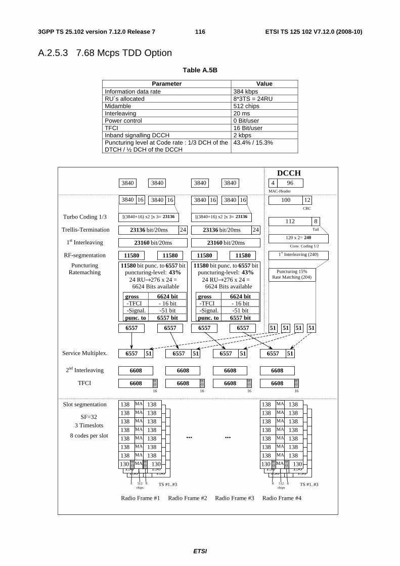
ETSI
ETSI TS 125 102 V7.12.0 (2008-10) 1163GPP TS 25.102 version 7.12.0 Release 7
A.2.5.3 7.68 Mcps TDD Option
Table A.5B
Parameter Value Information data rate 384 kbps RU´s allocated 8*3TS = 24RU Midamble 512 chips Interleaving 20 ms Power control 0 Bit/user TFCI 16 Bit/user Inband signalling DCCH 2 kbps Puncturing level at Code rate : 1/3 DCH of the DTCH / ½ DCH of the DCCH
43.4% / 15.3%
Turbo Coding 1/3 [(3840+16) x2 ]x 3= 23136
24 Trellis-Termination
1 st Interleaving
23136 bit/20ms
23160 bit/20ms
Puncturing Ratemaching
11580 bit punc. to 6557 bit puncturing-level: 43%
24 RU → 276 x 24 = 6624 Bits available
gross 6624 bit -TFCI - 16 bit -Signal. -51 bit punc. to 6557 bit
SF=32 3 Timeslots
8 codes per slot
Service Multiplex.
2 nd Interleaving
96 4
100 12
8 Tail
CRC
MAC-Header
112
120 x 2= 240 Conv. Coding 1/2
6557 6557 6557 6557
TF CI 16
DCCH
6557 6557 6557 6557 51 51 51 51
51 51 51 51
6608 6608 6608
Slot segmentation
6608
6608 TF CI 16
6608 TF CI 16
6608 TF CI 16
6608 TFCI
Puncturing 15% Rate Matching (204)
Radio Frame #1 Radio Frame #2 Radio Frame #3 Radio Frame #4
1 st Interleaving (240)
TS #1..#3
... ...
138 138 MA 138 138 MA 138 138 MA 138 138 MA 138 138 MA 138 138 MA 138 138 MA 138 138 MA
138 138 MA 138 138 MA 138 138 MA 138 138 MA 138 138 MA 138 138 MA 138 138 MA 138 138 MA 130 130 TF
CI TF CI MA
138 138 MA 138 138 MA 138 138 MA 138 138 MA 138 138 MA 138 138 MA 138 138 MA
8 8 512 chips
138 138 MA 138 138 MA 138 138 MA 138 138 MA 138 138 MA 138 138 MA 138 138 MA 138 138 MA
138 138 MA 138 138 MA 138 138 MA 138 138 MA 138 138 MA 138 138 MA 138 138 MA 138 138 MA 130 130 TF
CI TF CI MA
138 138 MA 138 138 MA 138 138 MA 138 138 MA 138 138 MA 138 138 MA 138 138 MA
8 8 512 chips TS #1..#3
RF-segmentation 11580 11580
3840
3840 16
3840
3840
[(3840+16) x2 ]x 3= 23136
24 23136 bit/20ms
23160 bit/20ms
11580 bit punc. to 6557 bit puncturing-level: 43%
24 RU → 276 x 24 = 6624 Bits available
gross 6624 bit -TFCI - 16 bit -Signal. -51 bit punc. to 6557 bit
16
11580 11580
3840
3840 16
3840
3840 16

ETSI
ETSI TS 125 102 V7.12.0 (2008-10) 1173GPP TS 25.102 version 7.12.0 Release 7
Figure A.5B
A.2.6 BCH reference measurement channel [mapped to 1 code SF16]
A.2.6.1 3.84 Mcps TDD Option
Table A.6
Parameter Value Information data rate: 12.3 kbps RU´s allocated 1 RU Midamble 512 chips Interleaving 20 ms Power control 0 bit TFCI 0 bit Puncturing level 10%
Information data 246
246CRC attachment
Tail bit attachment
[(262+8)]x2=540
8
ConvolutionalCoding 1/2
1st Interleaving
262
540
PuncturingRatemaching
SF=16 122 122512
chips
16
RF-segmentation 270 270
Slot segmentation
122 122512
chips
Radio Frame #1 Radio Frame #2
MAMA
270 bit punc. to 244 bitpuncturing-level: 10%
2nd Interleaving 244 244
Figure A.6
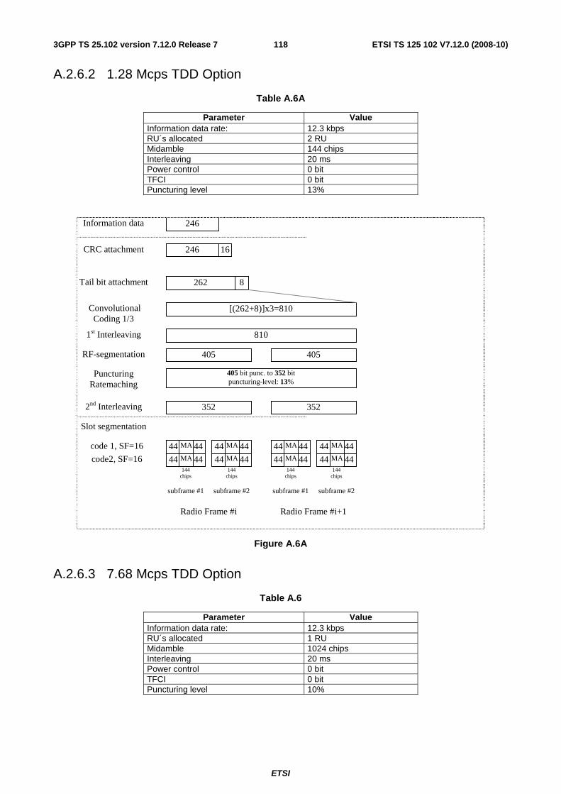
ETSI
ETSI TS 125 102 V7.12.0 (2008-10) 1183GPP TS 25.102 version 7.12.0 Release 7
A.2.6.2 1.28 Mcps TDD Option
Table A.6A
Parameter Value Information data rate: 12.3 kbps RU´s allocated 2 RU Midamble 144 chips Interleaving 20 ms Power control 0 bit TFCI 0 bit Puncturing level 13%
44 44
Information data 246
246 CRC attachment
Tail bit attachment
[(262+8)]x3=810
8
Convolutional Coding 1/3
1st Interleaving
262
810
Puncturing Ratemaching
code 1, SF=16
144 chips
16
RF-segmentation 405 405
Slot segmentation
Radio Frame #i
405 bit punc. to 352 bit puncturing-level: 13%
2nd Interleaving 352 352
MA
code2, SF=16 44 44 MA
44 44 44 44 44 44
44 44 44 44 44 44
MA
MA
MA
MA
MA
MA
144 chips
144 chips
144 chips
subframe #1 subframe #1 subframe #2 subframe #2
Radio Frame #i+1
Figure A.6A
A.2.6.3 7.68 Mcps TDD Option
Table A.6
Parameter Value Information data rate: 12.3 kbps RU´s allocated 1 RU Midamble 1024 chips Interleaving 20 ms Power control 0 bit TFCI 0 bit Puncturing level 10%

ETSI
ETSI TS 125 102 V7.12.0 (2008-10) 1193GPP TS 25.102 version 7.12.0 Release 7
Information data 246
246 CRC attachment
Tail bit attachment
[(262+8)]x2=540
8
Convolutional Coding 1/2
1 st Interleaving
262
540
Puncturing Ratemaching
SF=32 122 122 1024
chips
16
RF-segmentation 270 270
Slot segmentation
122 122 1024
chips
Radio Frame #1 Radio Frame #2
MA MA
270 bit punc. to 244 bit puncturing-level: 10 %
2 nd
Interleaving 244 244
Figure A.6B
A.2.7 UL multi code reference measurement channel (12.2 kbps)
A.2.7.1 3.84 Mcps TDD Option
Table A.7
Parameter Value Information data rate 12.2 kbps RU´s allocated 2 RU Midamble 512 chips Interleaving 20 ms Power control 2 Bit/user TFCI 16 Bit/user Inband signalling DCCH 2 kbps Puncturing level at Code rate 1/3 : DCH of the DTCH / DCH of the DCCH
5% / 0 %

ETSI
ETSI TS 125 102 V7.12.0 (2008-10) 1203GPP TS 25.102 version 7.12.0 Release 7
Information data 244
244CRC attachment
Tail bit attachment
[(260 +8)]x 3= 804
8
Conv. Coding 1/3
1st Interleaving
260 bit/20ms
804 bit/20ms
PuncturingRatemaching
402 bit punct. to 380 bitpuncturing-level: 5%
2 RU→244x2 = 488 Bits available
gross 488 bit -TFCI -TPC
-16 bit-2 bit
-Signal. -90 bitpunc. to 380 bit
SF=16
114 1128 512
chips
Service Multiplex.
2nd Interleaving
24416 16
244 964
100 12
8 Tail
CRC
MAC-Header
112
120 x 3= 360
Conv. Coding 1/3
380 380 380 380
DCCH
380 380 380 380 90 90 90 90
90 90 90 90
470 470 470
Slot segmentation
470
470 470 470 470TFCI
Repetition 0%Rate Matching (360)
114 112TFCI
8 512chips
114 112TFCI
8 512chips
114 112TFCI
8 512chips
Radio Frame #1 Radio Frame #2 Radio Frame #3 Radio Frame #4
MA MA MAMA
1st Interleaving (360)
[(260 +8)]x 3= 804
8260 bit/20ms
804 bit/20ms
122 122 122 122 122 122 122 122MA MA MAMA
RF-segmentation 402 402 402 402
402 bit punct. to 380 bitpuncturing-level: 5%
2 RU→244x2 = 488 Bits available
gross 488 bit -TFCI -TPC
-16 bit-2 bit
-Signal. -90 bitpunc. to 380 bit
TFCI
TPC
TFCI
TPC
TFCI
TPC
TFCI
TPC
TFCI
2 8 2 8 2 8 2 8
TFCI
TPC
TFCI
TPC
TFCI
TPC
TFCI
TPC
16 2 16 2 16 2 16 2
Figure A.7
A.2.7.2 1.28 Mcps TDD Option
Table A.7A
Parameter Value Information data rate 12.2 kbps RU's allocated 1TS (2*SF16) =
2RU/5ms Midamble 144 Interleaving 20 ms Power control (TPC) 4 Bit/user/10ms TFCI 16 Bit/user/10ms 4 Bit reserved for future use (place of SS) 4 Bit/user/10ms Inband signalling DCCH 2.4 kbps Puncturing level at Code rate 1/3: DCH of the DTCH / DCH of the DCCH
33% / 33%

ETSI
ETSI TS 125 102 V7.12.0 (2008-10) 1213GPP TS 25.102 version 7.12.0 Release 7
244
244 16
260bit/20ms 8
(260+8)*3=804
804bit/20ms
402 402
268 268
268 26860 60
328 328
176
328 16 8 328 16 8
176 176 176
Information Data
CRC attachement
Tail bit attachement
Conv. Coding 1/3
1st Interleaving
RF-Segmentation
Rate Matching
Service Multiplexing
2st Interleaving
TFCI, TPC and SS
Physical Channel Mapping
402 bit puncturing to 268 bitPuncturing Level: 33%
4 RU = 88 * 4 = 352 Bits available
gross
- TFCI- TPC- Reserved
- Signalling
puncturing to
352 bit
- 16 bit- 4 bit- 4 bit
- 60 bit
268 bit
4
100 12
112 8
(112+8)*3=360
360bit
60
Puncturing Level: 33%Rate Matching (240)
96
60 6060
328 16 8 328 16 8
176 176 176
402 bit puncturing to 268 bitPuncturing Level: 33%
4 RU = 88 * 4 = 352 Bits available
gross
- TFCI- TPC- Reserved
- Signalling
puncturing to
352 bit
- 16 bit- 4 bit- 4 bit
- 60 bit
268 bit
36440 4144
chips 4
44 144chips
44
36440 4144
chips 4
44 144chips
44
36440 4144
chips 4
44 144chips
44
36440 4144
chips 4
44 144chips
44Slot segmentation SF=16
Sub Frame #1 Sub Frame #2 Sub Frame #3 Sub Frame #4 Sub Frame #5 Sub Frame #6 Sub Frame #7 Sub Frame #8
DCCH
TFCITPC &Reserved
TFCI
36
MAC-Header
440 4144
chips 4
44144chips
44
SF=16 36440 4144
chips 4
44144chips
44
36440 4144
chips 4
44144chips
44
36440 4144
chips 4
44144chips
44
244
244 16
260bit/20ms 8
(260+8)*3=804
804bit/20ms
402 402
268 268
268 26860 60
328 328
176
Figure A.7A
A.2.7.3 7.68 Mcps TDD Option
Table A.7B
Parameter Value Information data rate 12.2 kbps RU´s allocated 2 RU Midamble 1024 chips Interleaving 20 ms Power control 2 Bit/user TFCI 16 Bit/user Inband signalling DCCH 2 kbps Puncturing level at Code rate 1/3 : DCH of the DTCH / DCH of the DCCH
5% / 0 %
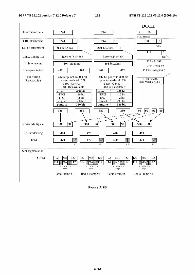
ETSI
ETSI TS 125 102 V7.12.0 (2008-10) 1223GPP TS 25.102 version 7.12.0 Release 7
Information data 244
244 CRC attachment
Tail bit attachment
[(260 +8)]x 3= 804
8
Conv. Coding 1/3
1 st Interleaving
260 bit/20ms
804 bit/20ms
Puncturing Ratemaching
402 bit punct. to 380 bit puncturing-level: 5%
2 RU → 244x2 = 488 Bits available
gross 488 bit -TFCI -TPC
-16 bit -2 bit
-Signal. -90 bit punc. to 380 bit
SF=32 114 112
8 1024 chips
Service Multiplex.
2 nd Interleaving
244 16 16
244 96 4
100 12
8 Tail
CRC
MAC-Header
112
120 x 3= 360 Conv. Coding 1/3
380 380 380 380
DCCH
380 380 380 380 90 90 90 90
90 90 90 90
470 470 470
Slot segmentation
470
470 470 470 470 TFCI
Repetition 0% Rate Matching (360)
114 112 TF CI 8 1024
chips
114 112 TF CI 8 1024
chips
114 112 TF CI 8 1024
chips
Radio Frame #1 Radio Frame #2 Radio Frame #3 Radio Frame #4
MA MA MA MA
1 st Interleaving (360)
[(260 +8)]x 3= 804
8 260 bit/20ms
804 bit/20ms
122 122 122 122 122 122 122 122 MA MA MA MA
RF-segmentation 402 402 402 402
402 bit punct. to 380 bit puncturing-level: 5%
2 RU → 244x2 = 488 Bits available
gross 488 bit -TFCI -TPC
-16 bit -2 bit
-Signal. -90 bit punc. to 380 bit
TF CI TP
C TF CI TP
C TF CI TP
C TF CI TP
C TF CI
2 8 2 8 2 8 2 8
TF CI TP
C TF CI TP
C TF CI TP
C TF CI TP
C 16 2 16 2 16 2 16 2
Figure A.7B
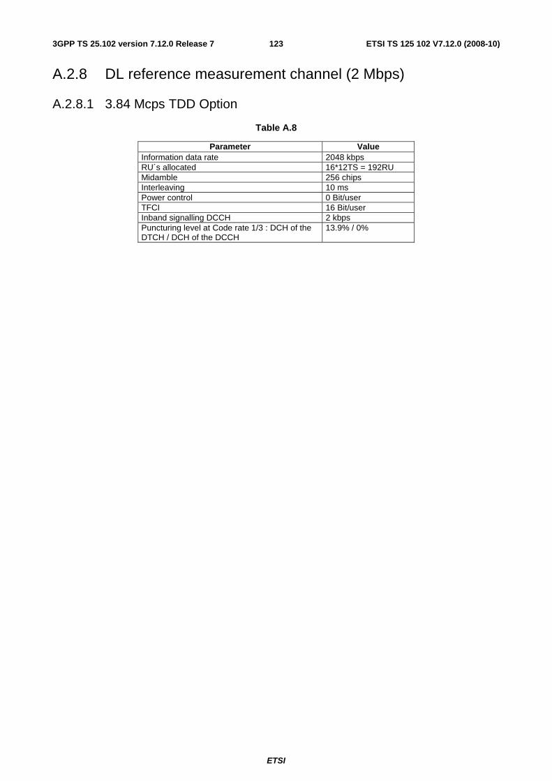
ETSI
ETSI TS 125 102 V7.12.0 (2008-10) 1233GPP TS 25.102 version 7.12.0 Release 7
A.2.8 DL reference measurement channel (2 Mbps)
A.2.8.1 3.84 Mcps TDD Option
Table A.8
Parameter Value Information data rate 2048 kbps RU´s allocated 16*12TS = 192RU Midamble 256 chips Interleaving 10 ms Power control 0 Bit/user TFCI 16 Bit/user Inband signalling DCCH 2 kbps Puncturing level at Code rate 1/3 : DCH of the DTCH / DCH of the DCCH
13.9% / 0%
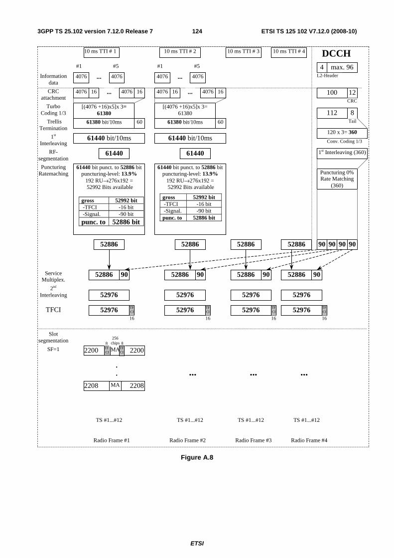
ETSI
ETSI TS 125 102 V7.12.0 (2008-10) 1243GPP TS 25.102 version 7.12.0 Release 7
Informationdata
4076
CRCattachment
TurboCoding 1/3
[(4076 +16)x5]x 3=61380
60 TrellisTermination
1st
Interleaving
61380 bit/10ms
61440 bit/10ms
PuncturingRatemaching
61440 bit punct. to 52886 bitpuncturing-level: 13.9%
192 RU→276x192 = 52992 Bits available
gross 52992 bit -TFCI -16 bit -Signal. -90 bit
punc. to 52886 bit
ServiceMultiplex.
2nd
Interleaving
16
max. 964
100 12
8 Tail
CRC
L2-Header
112
120 x 3= 360
Conv. Coding 1/3
52886 52886 52886 52886
TFCI
16
DCCH
52886 52886 52886 52886 90 90 90 90
90 90 90 90
52976 52976
Slotsegmentation
52976
52976 TFCI
16
52976 TFCI
16
52976 TFCI
16
52976TFCI
Puncturing 0%Rate Matching
(360)
1st Interleaving (360)
Radio Frame #1 Radio Frame #2 Radio Frame #3 Radio Frame #4
TS #1...#12
... ...
RF-segmentation
61440
4076...
#1 #5
4076 4076... 16
4076
[(4076 +16)x5]x 3=61380
6061380 bit/10ms
61440 bit/10ms
61440 bit punct. to 52886 bitpuncturing-level: 13.9%
192 RU→276x192 = 52992 Bits available
gross 52992 bit -TFCI -16 bit -Signal. -90 bitpunc. to 52886 bit
16
61440
4076...
#1 #5
4076 4076... 16
SF=1
TS #1...#12
52976
10 ms TTI # 1 10 ms TTI # 2 10 ms TTI # 3 10 ms TTI # 4
2200 2200MATFCI
8256
chips8
.
.
2208 2208234
MA
TFCI
TS #1...#12 TS #1...#12
...
Figure A.8

ETSI
ETSI TS 125 102 V7.12.0 (2008-10) 1253GPP TS 25.102 version 7.12.0 Release 7
A.2.8.2 1.28 Mcps TDD Option
Table A.8A
Parameter Value Information data rate 2048 kbps RU's allocated 5TS (1*SF1) =
80RU/5ms Midamble 144 Interleaving 10 ms Power control (TPC) 6 Bit/user/10ms TFCI 48 Bit/user/10ms Synchronisation Shift (SS) 6 Bit/user/10ms Inband signalling DCCH no Coding no Modulation 8PSK
20480
5120
Information Data
Transport Blocksegmentation
Block CRCattachement
Conv. Coding: no
Rate matching
Service Multiplexing: no
2nd Interleaving
Physical Channel Mapping
5120 5120 5120
245120 245120 245120 245120
1st interleaving: no
Code blockconcatenation
20576
Puncturing Level: NA160 RU = 132 * 160 = 21120 Bits available
gross
- TFCI- TPC- SS
- Signalling
rate matching to
21120 bit
- 48 bit- 6 bit- 6 bit
- no
21060 bit
21060
Subframe segmentation 10530
Adding TFCI, TPC, SS
10530
310530 24 3 310530 24 3
Time Slot #i+4
Time Slot #i+3
Time Slot #i+2
Time Slot #i+1
Time Slot #i
1056 1056144chips
1044 1038144chips
12 126
Subframe #1
Time Slot #i+4
Time Slot #i+3
Time Slot #i+2
Time Slot #i+1
Time Slot #i 1044 1038144chips
12 126
Subframe #2
1056 1056144chips
1056 1056144chips
1056 1056144chips
1056 1056144chips
1056 1056144chips
1056 1056144chips
1056 1056144chips
Figure A.8A

ETSI
ETSI TS 125 102 V7.12.0 (2008-10) 1263GPP TS 25.102 version 7.12.0 Release 7
A.2.8.3 7.68 Mcps TDD Option
Table A.8B
Parameter Value Information data rate 2048 kbps RU´s allocated 16*12TS = 192RU Midamble 512 chips Interleaving 10 ms Power control 0 Bit/user TFCI 16 Bit/user Inband signalling DCCH 2 kbps Puncturing level at Code rate 1/3 : DCH of the DTCH / DCH of the DCCH
13.9% / 0%

ETSI
ETSI TS 125 102 V7.12.0 (2008-10) 1273GPP TS 25.102 version 7.12.0 Release 7
Information data
4076
CRC attachment
Turbo Coding 1/3
[(4076 +16 )x5]x 3 = 61380
60 Trellis Termination
1 st Interleaving
61380 bit/10ms
61440 bit/10ms
Puncturing Ratemaching
61440 bit punct . to 52886 bit puncturing-level: 13.9%
192 RU → 276x192 = 52992 Bits available
gross 52992 bit -TFCI -16 bit -Signal. -90 bit punc. to 52886 bit
Service Multiplex.
2 nd Interleaving
16
max. 96 4
100 12
8 Tail
CRC
L2-Header
112
120 x 3= 360 Conv. Coding 1/3
52886 52886 52886 52886
TF CI 16
DCCH
52886 52886 52886 52886 90 90 90 90
90 90 90 90
52976 52976
Slot segmentation
52976
52976 TF CI 16
52976 TF CI 16
52976 TF CI 16
52976 TFCI
Puncturing 0% Rate Matching
(360)
1 st Interleaving (360)
TS #1...#12
... ...
RF- segmentation
61440
4076 ...
#1 #5
4076 4076 ... 16
4076
[(4076 +16 )x5]x 3= 61380
60 61380 bit/10ms
61440 bit/10ms
61440 bit punct . to 52886 bit puncturing-level: 13.9%
192 RU → 276x192 = 52992 Bits available
gross 52992 bit -TFCI -16 bit -Signal. -90 bit punc. to 52886 bit
16
61440
4076 ...
#1 #5
4076 4076 ... 16
SF=2
TS #1...#12
52976
10 ms TTI # 1 10 ms TTI # 2 10 ms TTI # 3 10 ms TTI # 4
2200 2200 MA TF CI
8 512
chips 8
.
.
2208 2208 234
MA
TF CI
TS #1...#12 TS #1...#12
...
Figure A.8B
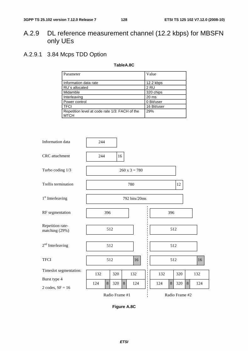
ETSI
ETSI TS 125 102 V7.12.0 (2008-10) 1283GPP TS 25.102 version 7.12.0 Release 7
A.2.9 DL reference measurement channel (12.2 kbps) for MBSFN only UEs
A.2.9.1 3.84 Mcps TDD Option
TableA.8C
Parameter Value
Information data rate 12.2 kbps RU´s allocated 2 RU Midamble 320 chips Interleaving 20 ms Power control 0 Bit/user TFCI 16 Bit/user Repetition level at code rate 1/3: FACH of the MTCH
29%
Figure A.8C
Information data
CRC attachment
Turbo coding 1/3
Trellis termination
1st Interleaving
RF segmentation
Repetition rate-matching (29%)
244
244 16
260 x 3 = 780
780 12
792 bits/20ms
396
512
2nd Interleaving 512
TFCI 512 16
Timeslot segmentation:
Burst type 4
2 codes, SF = 16
132
8
320
8 124 124
Radio Frame #1
396
512
512
512 16
132
320
132
8
320
8 124 124
132
320
Radio Frame #2
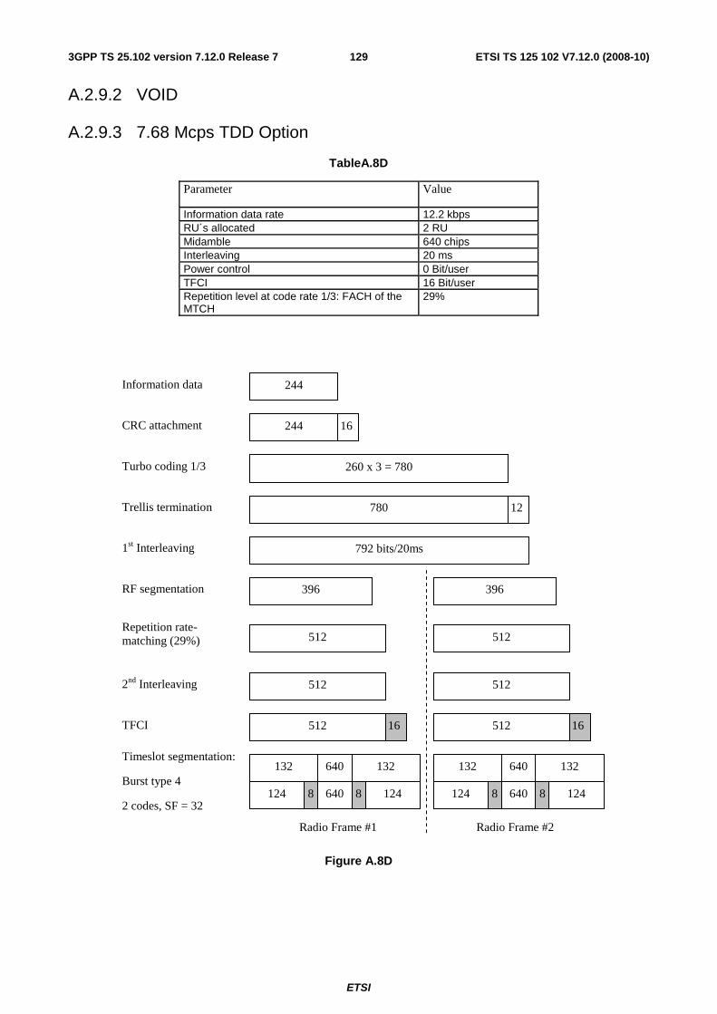
ETSI
ETSI TS 125 102 V7.12.0 (2008-10) 1293GPP TS 25.102 version 7.12.0 Release 7
A.2.9.2 VOID
A.2.9.3 7.68 Mcps TDD Option
TableA.8D
Parameter Value
Information data rate 12.2 kbps RU´s allocated 2 RU Midamble 640 chips Interleaving 20 ms Power control 0 Bit/user TFCI 16 Bit/user Repetition level at code rate 1/3: FACH of the MTCH
29%
Figure A.8D
Information data
CRC attachment
Turbo coding 1/3
Trellis termination
1st Interleaving
RF segmentation
Repetition rate-matching (29%)
244
244 16
260 x 3 = 780
780 12
792 bits/20ms
396
512
2nd Interleaving 512
TFCI 512 16
Timeslot segmentation:
Burst type 4
2 codes, SF = 32
132
8
640
8 124 124
Radio Frame #1
396
512
512
512 16
132
640
132
8
640
8 124 124
132
640
Radio Frame #2

ETSI
ETSI TS 125 102 V7.12.0 (2008-10) 1303GPP TS 25.102 version 7.12.0 Release 7
A.3 HSDPA reference measurement channels
A.3.1 HSDPA reference measurement channels for 3,84 Mcps TDD option
A.3.1.1 Reference measurement channels for 7,3 Mbps - Category 8 - UE
A.3.1.1.1 QPSK modulation scheme for test 1, 2, 3
Table A.9: HS-PDSCH fixed reference channel for the PA3, PB3, and VA30 Channel models - Category 8
Parameter Unit Value Maximum information bit throughput Mbps 2,6496 Number of HARQ Processes Processes 4 Information Bit Payload ( INFN ) Bits 26496
Number Code Blocks Blocks 6 Total Available of Soft Channel bits in UE Bits 353280 Number of Soft Channel bit per HARQ Proc. Bits 88320 Number of coded bits per TTI Bits 35328 Coding Rate 3/4 Number of HS-PDSCH Timeslots Slots 8 Number of HS-PDSCH codes per TS Codes 16 Spreading factor SF 16
26496
26496
4420
3 x 4420 + 12 tail bits
79632
35328
Inf. Bit Payload
CRC addition
Code Block Segmentation
Turbo coding R=1/3
1st Rate Matching
2nd Rate Matching
Time Slot Segmentation16 codes/TS, 8 TS/TTI
CRC 24
4420 4420 4420
6 blocks of
4420 4420
35328 bits/10 ms
Figure A.9: Coding for HS-PDSCH fixed reference channel with QPSK modulation for the PA3, PB3, and VA30 Channels - Category 8

ETSI
ETSI TS 125 102 V7.12.0 (2008-10) 1313GPP TS 25.102 version 7.12.0 Release 7
A.3.1.1.2 QPSK modulation scheme for test 4
Table A.10: HS-PDSCH fixed reference channel for the VA120 Channel model - Category 8
Parameter Unit Value Maximum information bit throughput Mbps 2,3176 Number of HARQ Processes Processes 4 Information Bit Payload ( INFN ) Bits 23176
Number Code Blocks Blocks 5 Total Available of Soft Channel bits in UE Bits 353280 Number of Soft Channel bit per HARQ Proc. Bits 88320 Number of coded bits per TTI Bits 30912 Coding Rate 3/4 Number of HS-PDSCH Timeslots Slots 8 Number of HS-PDSCH codes per TS Codes 14 Spreading factor SF 16
23176
23176
4640
3 x 4640 + 12 tail bits
69660
30912
Inf. Bit Payload
CRC addition
Code Block Segmentation
Turbo coding R=1/3
1st Rate Matching
2nd Rate Matching
Time Slot Segmentation14 codes/TS, 8 TS/TTI
CRC 24
4640 4640 4640
5 blocks of
4640
30912 bits/10 ms
Figure A.10: Coding for HS-PDSCH fixed reference channel with QPSK modulation for the VA120 Channel - Category 8

ETSI
ETSI TS 125 102 V7.12.0 (2008-10) 1323GPP TS 25.102 version 7.12.0 Release 7
A.3.1.1.3 16QAM modulation scheme for test 1, 2, 3
Table A.11: HS-PDSCH fixed reference channel for the PA3, PB3, and VA30 Channel models - Category 8
Parameter Unit Value Modulation 16-QAM Maximum information bit throughput Mbps 5,2996 Number of HARQ Processes Processes 4 Information Bit Payload ( INFN ) Bits 52996
Number Code Blocks Blocks 11 Total Available of Soft Channel bits in UE Bits 353280 Number of Soft Channel bit per HARQ Proc. Bits 88320 Number of coded bits per TTI Bits 70656 Coding Rate 3/4 Number of HS-PDSCH Timeslots Slots 8 Number of HS-PDSCH codes per TS Codes 16 Spreading factor SF 16
52996
52996
3 x 4820 + 12 tail bits
88320
70656
Inf. Bit Payload
CRC addition
Code Block Segmentation
Turbo coding R=1/3
1st Rate Matching
2nd Rate Matching
Time Slot Segmentation16 codes/TS, 8 TS/TTI
CRC 24
11 blocks of
4820
70656 bits/10 ms
11 blocks of
Total 159192 bits
Figure A.11: Coding for HS-PDSCH fixed reference channel with 16-QAM modulation for the PA3 PB3, and VA30 Channels - Category 8

ETSI
ETSI TS 125 102 V7.12.0 (2008-10) 1333GPP TS 25.102 version 7.12.0 Release 7
A.3.1.1.4 16QAM modulation scheme for test 4
Table A.12: HS-PDSCH fixed reference channel for the PA3, PB3, and VA30 Channel models - Category 8
Parameter Unit Value Modulation 16-QAM Maximum information bit throughput Mbps 3,4773 Number of HARQ Processes Processes 4 Information Bit Payload ( INFN ) Bits 34773
Number Code Blocks Blocks 7 Total Available of Soft Channel bits in UE Bits 353280 Number of Soft Channel bit per HARQ Proc. Bits 88320 Number of coded bits per TTI Bits 61824 Coding Rate 9/16 Number of HS-PDSCH Timeslots Slots 8 Number of HS-PDSCH codes per TS Codes 14 Spreading factor SF 16
34773
34773
3 x 4971 + 12 tail bits
88320
61824
Inf. Bit Payload
CRC addition
Code Block Segmentation
Turbo coding R=1/3
1st Rate Matching
2nd Rate Matching
Time Slot Segmentation14 codes/TS, 8 TS/TTI
CRC 24
7 blocks of
4971
61824 bits/10 ms
7 blocks of
Total 104475 bits
Figure A.12: Coding for HS-PDSCH fixed reference channel with 16-QAM modulation for the VA120 Channel - Category 8
A.3.2 HSDPA reference measurement channels for 1.28 Mcps TDD option
A.3.2.1 Reference measurement channels for 0.5 Mbps UE class
A.3.2.1.1 QPSK modulation scheme
Table A.13-1
Parameter Value Maximum information data rate 199.2 kbps RU"s allocated 2TS(10*SF16)=20 RU/5ms Midamble 144chips Puncturing level at code rate 1/3 43%
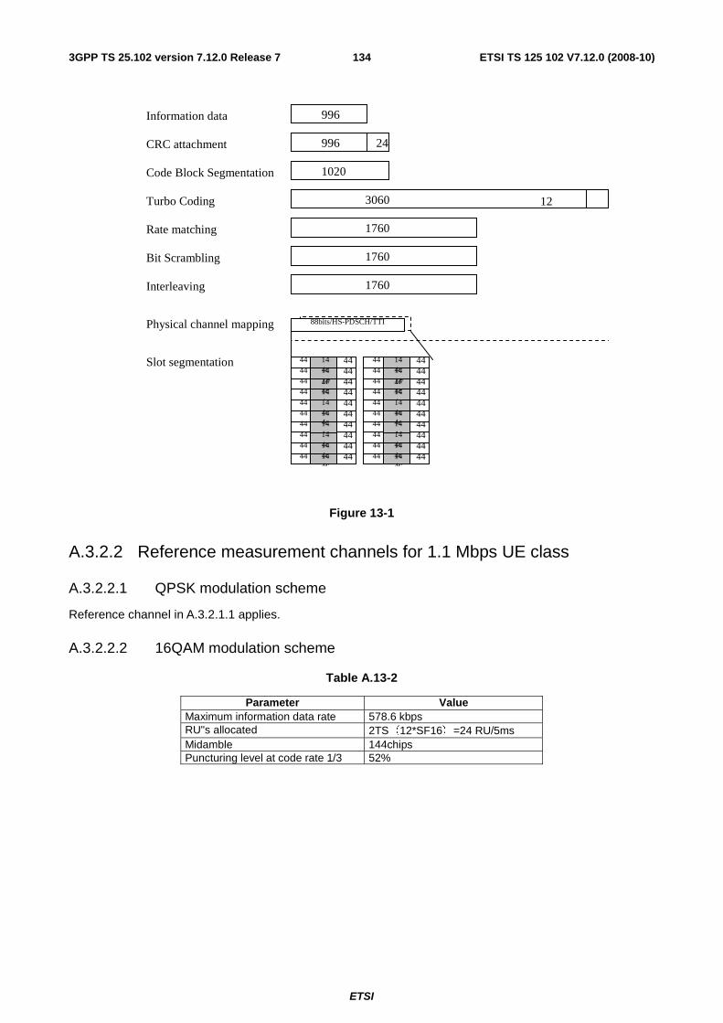
ETSI
ETSI TS 125 102 V7.12.0 (2008-10) 1343GPP TS 25.102 version 7.12.0 Release 7
12
Information data
CRC attachment
Code Block Segmentation
Rate matching
Turbo Coding
Bit Scrambling
Interleaving
Physical channel mapping
996
996 24
1020
3060
1760
1760
1760
44
44 44 44 44 44 44 44 44 44
44 44 44 44 44 44 44 44 44 44
144c 14
4c 144c 144c 144c 144c 144c 144c 144c 144c
44
44 44 44 44 44 44 44 44 44
44 44 44 44 44 44 44 44 44 44
144c 14
4c 144c 144c 144c 144c 144c 144c 144c 144c
Slot segmentation
88bits/HS-PDSCH/TTI
Figure 13-1
A.3.2.2 Reference measurement channels for 1.1 Mbps UE class
A.3.2.2.1 QPSK modulation scheme
Reference channel in A.3.2.1.1 applies.
A.3.2.2.2 16QAM modulation scheme
Table A.13-2
Parameter Value Maximum information data rate 578.6 kbps RU"s allocated 2TS(12*SF16)=24 RU/5ms Midamble 144chips Puncturing level at code rate 1/3 52%
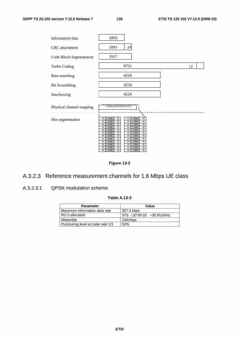
ETSI
ETSI TS 125 102 V7.12.0 (2008-10) 1353GPP TS 25.102 version 7.12.0 Release 7
12
Information data
CRC attachment
Code Block Segmentation
Rate matching
Turbo Coding
Bit Scrambling
Interleaving
Physical channel mapping
2893
2893 24
2917
8751
4224
4224
4224
Slot segmentation 88 88 144c 88 88 144c 88 88 144c 88 88 144c 88 88 144c 88 88 144c 88 88 144c 88 88 144c 88 88 144c 88 88 144c 88 88 144c 88 88 144c
88 88 144c 88 88 144c 88 88 144c 88 88 144c 88 88 144c 88 88 144c 88 88 144c 88 88 144c 88 88 144c 88 88 144c 88 88 144c 88 88 144c
176bits/HS-PDSCH/TTI
Figure 13-2
A.3.2.3 Reference measurement channels for 1.6 Mbps UE class
A.3.2.3.1 QPSK modulation scheme
Table A.13-3
Parameter Value Maximum information data rate 357.4 kbps RU"s allocated 3TS(10*SF16)=30 RU/5ms Midamble 144chips Puncturing level at code rate 1/3 52%
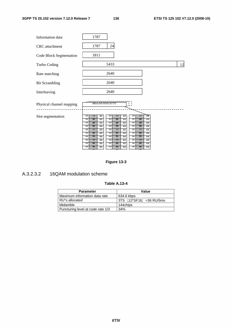
ETSI
ETSI TS 125 102 V7.12.0 (2008-10) 1363GPP TS 25.102 version 7.12.0 Release 7
Information data
CRC attachment
Code Block Segmentation
Rate matching
Turbo Coding
Bit Scrambling
Interleaving
Physical channel mapping
1787
1787 24
1811
5433
2640
2640
2640
Slot segmentation
44
44 44 44 44 44 44 44 44 44
44 44 44 44 44 44 44 44 44 44
144c 14
4c 144c 144c 144c 144c 144c 144c 144c 144c
44
44 44 44 44 44 44 44 44 44
44 44 44 44 44 44 44 44 44 44
144c 14
4c 144c 144c 144c 144c 144c 144c 144c 144c
44
44 44 44 44 44 44 44 44 44
44 44 44 44 44 44 44 44 44 44
144c 14
4c 144c 144c 144c 144c 144c 144c 144c 144c
12
88bits/HS-PDSCH/TTI
Figure 13-3
A.3.2.3.2 16QAM modulation scheme
Table A.13-4
Parameter Value Maximum information data rate 634.6 kbps RU"s allocated 3TS(12*SF16)=36 RU/5ms Midamble 144chips Puncturing level at code rate 1/3 34%

ETSI
ETSI TS 125 102 V7.12.0 (2008-10) 1373GPP TS 25.102 version 7.12.0 Release 7
Information data
CRC attachment
Code Block Segmentation
Rate matching
Turbo Coding
Bit Scrambling
Interleaving
Physical channel mapping
3173
3173 24
3197
9591
6336
6336
6336
Slot segmentation
12
88 88 144c 88 88 144c 88 88 144c 88 88 144c 88 88 144c 88 88 144c 88 88 144c 88 88 144c 88 88 144c 88 88 144c 88 88 144c 88 88 144c
88 88 144c 88 88 144c 88 88 144c 88 88 144c 88 88 144c 88 88 144c 88 88 144c 88 88 144c 88 88 144c 88 88 144c 88 88 144c 88 88 144c
88 88 144c 88 88 144c 88 88 144c 88 88 144c 88 88 144c 88 88 144c 88 88 144c 88 88 144c 88 88 144c 88 88 144c 88 88 144c 88 88 144c
176bits/HS-PDSCH/TTI
Figure A.13-4
A.3.2.4 Reference measurement channels for 2.2 Mbps UE class
A.3.2.4.1 QPSK modulation scheme
Table A.13-5
Parameter Value Maximum information data rate 539 kbps RU"s allocated 4TS(10*SF16)=40 RU/5ms Midamble 144chips Puncturing level at code rate 1/3 57%
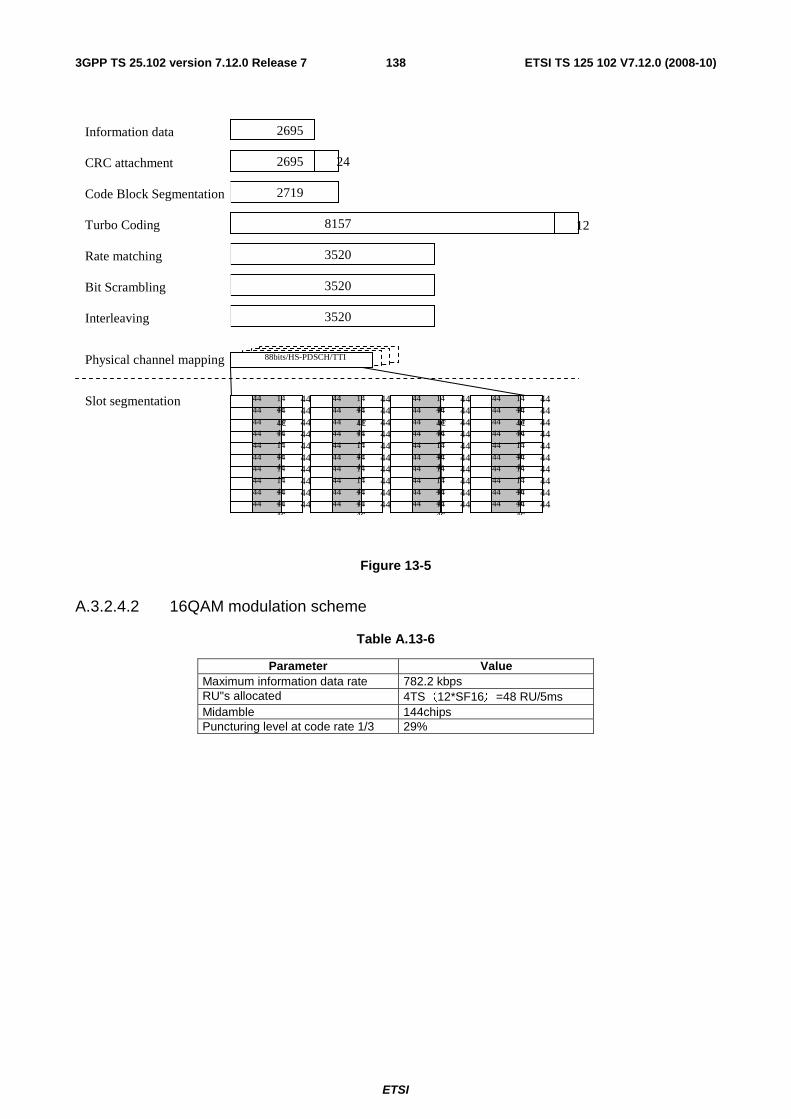
ETSI
ETSI TS 125 102 V7.12.0 (2008-10) 1383GPP TS 25.102 version 7.12.0 Release 7
12
Information data
CRC attachment
Code Block Segmentation
Rate matching
Turbo Coding
Bit Scrambling
Interleaving
Physical channel mapping
Slot segmentation
2695
2695 24
2719
8157
3520
3520
3520
44
44 44 44 44 44 44 44 44 44
44 44 44 44 44 44 44 44 44 44
144c 14
4c 144c 144c 144c 144c 144c 144c 144c 144c
44
44 44 44 44 44 44 44 44 44
44 44 44 44 44 44 44 44 44 44
144c 14
4c 144c 144c 144c 144c 144c 144c 144c 144c
44
44 44 44 44 44 44 44 44 44
44 44 44 44 44 44 44 44 44 44
144c 14
4c 144c 144c 144c 144c 144c 144c 144c 144c
44
44 44 44 44 44 44 44 44 44
44 44 44 44 44 44 44 44 44 44
144c 14
4c 144c 144c 144c 144c 144c 144c 144c 144c
88bits/HS-PDSCH/TTI
Figure 13-5
A.3.2.4.2 16QAM modulation scheme
Table A.13-6
Parameter Value Maximum information data rate 782.2 kbps RU"s allocated 4TS(12*SF16)=48 RU/5ms Midamble 144chips Puncturing level at code rate 1/3 29%

ETSI
ETSI TS 125 102 V7.12.0 (2008-10) 1393GPP TS 25.102 version 7.12.0 Release 7
12
Information data
CRC attachment
Code Block Segmentation
Rate matching
Turbo Coding
Bit Scrambling
Interleaving
Physical channel mapping
3911
3911 24
3935
11805
8448
8448
8448
Slot segmentation 88 88 144c 88 88 144c 88 88 144c 88 88 144c 88 88 144c 88 88 144c 88 88 144c 88 88 144c 88 88 144c 88 88 144c 88 88 144c 88 88 144c
88 88 144c 88 88 144c 88 88 144c 88 88 144c 88 88 144c 88 88 144c 88 88 144c 88 88 144c 88 88 144c 88 88 144c 88 88 144c 88 88 144c
88 88 144c 88 88 144c 88 88 144c 88 88 144c 88 88 144c 88 88 144c 88 88 144c 88 88 144c 88 88 144c 88 88 144c 88 88 144c 88 88 144c
88 88 144c 88 88 144c 88 88 144c 88 88 144c 88 88 144c 88 88 144c 88 88 144c 88 88 144c 88 88 144c 88 88 144c 88 88 144c 88 88 144c
176bits/HS-PDSCH/TTI
Figure 13-6
A.3.2.5 Reference measurement channels for 2.8 Mbps UE class
A.3.2.5.1 QPSK modulation scheme
Table A.13-7
Parameter Value Maximum information data rate 621 kbps RU"s allocated 5TS(10*SF16)=50 RU/5ms Midamble 144chips Puncturing level at code rate 1/3 53%
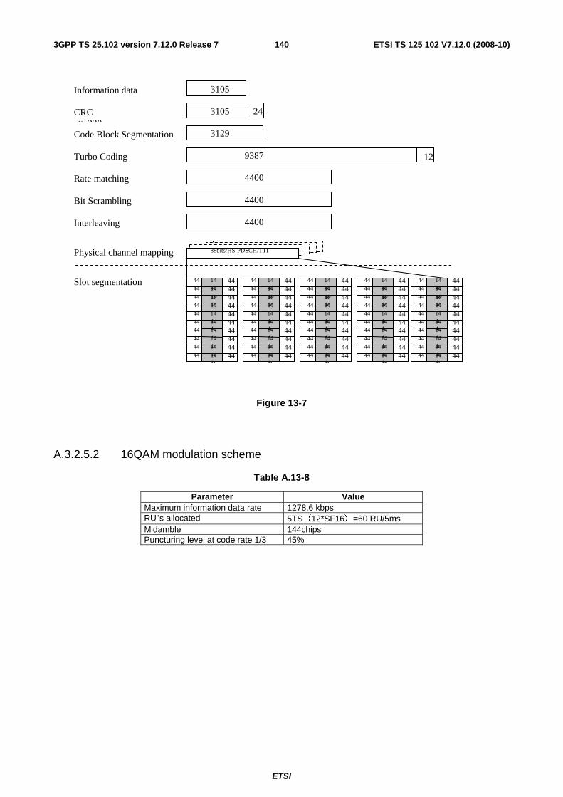
ETSI
ETSI TS 125 102 V7.12.0 (2008-10) 1403GPP TS 25.102 version 7.12.0 Release 7
Information data
CRC atta3208148148148148148
Code Block Segmentation
Rate matching
Turbo Coding
Bit Scrambling
Interleaving
Physical channel mapping
Slot segmentation
44
44 44 44 44 44 44 44 44 44
44 44 44 44 44 44 44 44 44 44
144c 14
4c 144c 144c 144c 144c 144c 144c 144c 144c
12
3105
3105 24
3129
9387
4400
4400
4400
44
44 44 44 44 44 44 44 44 44
44 44 44 44 44 44 44 44 44 44
144c 14
4c 144c 144c 144c 144c 144c 144c 144c 144c
44
44 44 44 44 44 44 44 44 44
44 44 44 44 44 44 44 44 44 44
144c 14
4c 144c 144c 144c 144c 144c 144c 144c 144c
44
44 44 44 44 44 44 44 44 44
44 44 44 44 44 44 44 44 44 44
144c 14
4c 144c 144c 144c 144c 144c 144c 144c 144c
44
44 44 44 44 44 44 44 44 44
44 44 44 44 44 44 44 44 44 44
144c 14
4c 144c 144c 144c 144c 144c 144c 144c 144c
88bits/HS-PDSCH/TTI
Figure 13-7
A.3.2.5.2 16QAM modulation scheme
Table A.13-8
Parameter Value Maximum information data rate 1278.6 kbps RU"s allocated 5TS(12*SF16)=60 RU/5ms Midamble 144chips Puncturing level at code rate 1/3 45%
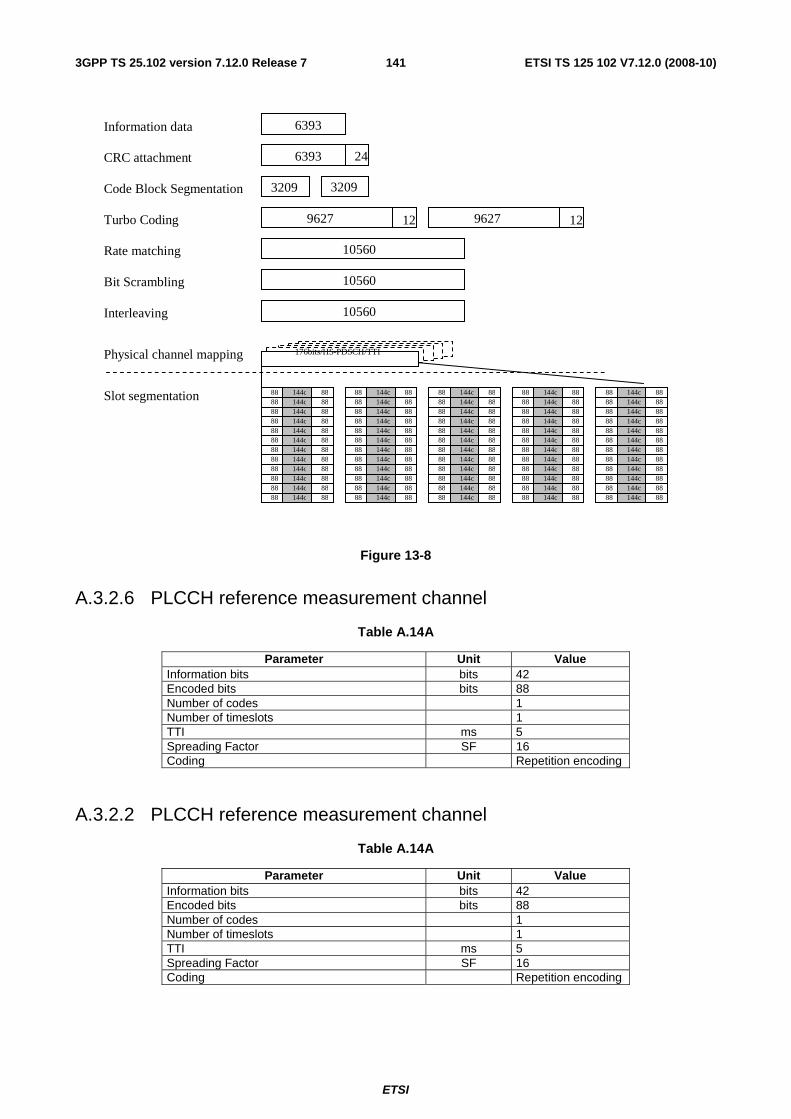
ETSI
ETSI TS 125 102 V7.12.0 (2008-10) 1413GPP TS 25.102 version 7.12.0 Release 7
Information data
CRC attachment
Code Block Segmentation
Rate matching
Turbo Coding
Bit Scrambling
Interleaving
Physical channel mapping
Slot segmentation
6393
6393 24
3209
9627
10560
10560
10560
12
88 88 144c 88 88 144c 88 88 144c 88 88 144c 88 88 144c 88 88 144c 88 88 144c 88 88 144c 88 88 144c 88 88 144c 88 88 144c 88 88 144c
88 88 144c 88 88 144c 88 88 144c 88 88 144c 88 88 144c 88 88 144c 88 88 144c 88 88 144c 88 88 144c 88 88 144c 88 88 144c 88 88 144c
88 88 144c 88 88 144c 88 88 144c 88 88 144c 88 88 144c 88 88 144c 88 88 144c 88 88 144c 88 88 144c 88 88 144c 88 88 144c 88 88 144c
88 88 144c 88 88 144c 88 88 144c 88 88 144c 88 88 144c 88 88 144c 88 88 144c 88 88 144c 88 88 144c 88 88 144c 88 88 144c 88 88 144c
3209
12 9627
176bits/HS-PDSCH/TTI
88 88 144c 88 88 144c 88 88 144c 88 88 144c 88 88 144c 88 88 144c 88 88 144c 88 88 144c 88 88 144c 88 88 144c 88 88 144c 88 88 144c
Figure 13-8
A.3.2.6 PLCCH reference measurement channel
Table A.14A
Parameter Unit Value Information bits bits 42 Encoded bits bits 88 Number of codes 1 Number of timeslots 1 TTI ms 5 Spreading Factor SF 16 Coding Repetition encoding
A.3.2.2 PLCCH reference measurement channel
Table A.14A
Parameter Unit Value Information bits bits 42 Encoded bits bits 88 Number of codes 1 Number of timeslots 1 TTI ms 5 Spreading Factor SF 16 Coding Repetition encoding

ETSI
ETSI TS 125 102 V7.12.0 (2008-10) 1423GPP TS 25.102 version 7.12.0 Release 7
A.3.2A HSDPA reference measurement channels for 7,68 Mcps TDD option
A.3.2A.1 Reference measurement channels for 5,3 Mbps - Category 8 - UE
A.3.2A.1.1 QPSK modulation scheme for test 1, 2, 3 & 4
Table A.15: HS-PDSCH fixed reference channel for the PA3, PB3, VA30 and VA120 Channel models - Category 8
Parameter Unit Value Maximum information bit throughput Mbps 1.7612 Number of HARQ Processes Processes 3 Information Bit Payload ( INFN ) Bits 17612
Number Code Blocks Blocks 4 Total Available of Soft Channel bits in UE Bits 211968 Number of Soft Channel bit per HARQ Proc. Bits 70656 Number of coded bits per TTI Bits 35328 Coding Rate 1/2 Number of HS-PDSCH Timeslots Slots 4 Number of HS-PDSCH codes per TS Codes 32 Spreading factor SF 32
Inf. Bit Payload 17612
CRC addition 17612 CRC 24
Code Block Segmentation 4409 4409 4409 4409
Turbo coding R=1/3 3 × 4409 + 12 tail bits 4 blocks of
1st Rate Matching 52956
2nd Rate Matching 35328
Time slot segmentation 32 codes/TS, 4 TS/TTI 35328 bits/10 ms
Figure A.15: Coding for HS-PDSCH fixed reference channel with QPSK modulation for the PA3, PB3, VA30 and VA120 Channels - Category 8

ETSI
ETSI TS 125 102 V7.12.0 (2008-10) 1433GPP TS 25.102 version 7.12.0 Release 7
A.3.2A.1.2 16QAM modulation scheme for test 1, 2, 3 & 4
Table A.16: HS-PDSCH fixed reference channel for the PA3, PB3, VA30 and VA120 Channel models - Category 8
Parameter Unit Value Modulation 16-QAM Maximum information bit throughput Mbps 3.5066 Number of HARQ Processes Processes 3 Information Bit Payload ( INFN ) Bits 35066
Number Code Blocks Blocks 7 Total Available of Soft Channel bits in UE Bits 211968 Number of Soft Channel bit per HARQ Proc. Bits 70656 Number of coded bits per TTI Bits 70656 Coding Rate ½ Number of HS-PDSCH Timeslots Slots 4 Number of HS-PDSCH codes per TS Codes 32 Spreading factor SF 32
Inf. Bit Payload 35066
CRC addition 35066 CRC 24
Code Block Segmentation 5013
Turbo coding R=1/3 3 × 5013 + 12 tail bits 7 blocks of
1st Rate Matching 70656
2nd Rate Matching 70656
Time slot segmentation 32 codes/TS, 4 TS/TTI 70656 bits/10 ms
7 blocks of
= 105357 bits
Figure A.16: Coding for HS-PDSCH fixed reference channel with 16-QAM modulation for the PA3 PB3, VA30 and VA120 Channels - Category 8
A.3.3 Variable Reference Channel definition for 3,84 Mcps and 1,28 Mcps TDD options
The variable reference measurement channels are defined by:
a) The maximum information bit payload that is determined by the UE capability class under test and the allocated resource units (and hence implicitly by the CQI table applicable to the UE under test as derived from TS25.321).
b) The most recently received UE CQI report.
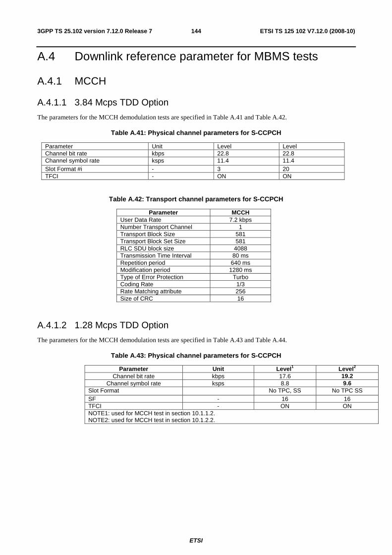
ETSI
ETSI TS 125 102 V7.12.0 (2008-10) 1443GPP TS 25.102 version 7.12.0 Release 7
A.4 Downlink reference parameter for MBMS tests
A.4.1 MCCH
A.4.1.1 3.84 Mcps TDD Option
The parameters for the MCCH demodulation tests are specified in Table A.41 and Table A.42.
Table A.41: Physical channel parameters for S-CCPCH
Parameter Unit Level Level Channel bit rate kbps 22.8 22.8 Channel symbol rate ksps 11.4 11.4 Slot Format #i - 3 20 TFCI - ON ON
Table A.42: Transport channel parameters for S-CCPCH
Parameter MCCH User Data Rate 7.2 kbps Number Transport Channel 1 Transport Block Size 581 Transport Block Set Size 581 RLC SDU block size 4088 Transmission Time Interval 80 ms Repetition period 640 ms Modification period 1280 ms Type of Error Protection Turbo Coding Rate 1/3 Rate Matching attribute 256 Size of CRC 16
A.4.1.2 1.28 Mcps TDD Option
The parameters for the MCCH demodulation tests are specified in Table A.43 and Table A.44.
Table A.43: Physical channel parameters for S-CCPCH
Parameter Unit Level1 Level2
Channel bit rate kbps 17.6 19.2 Channel symbol rate ksps 8.8 9.6
Slot Format No TPC, SS No TPC SS SF - 16 16 TFCI - ON ON NOTE1: used for MCCH test in section 10.1.1.2. NOTE2: used for MCCH test in section 10.1.2.2.
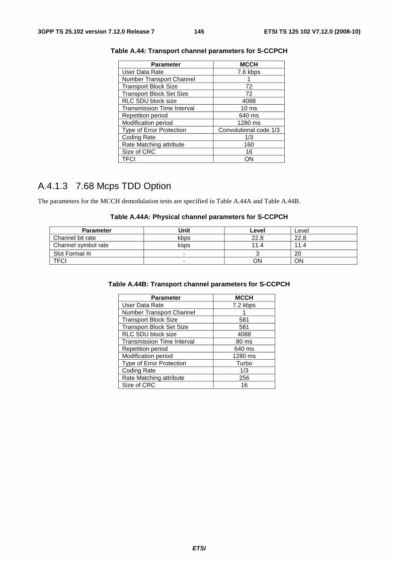
ETSI
ETSI TS 125 102 V7.12.0 (2008-10) 1453GPP TS 25.102 version 7.12.0 Release 7
Table A.44: Transport channel parameters for S-CCPCH
Parameter MCCH User Data Rate 7.6 kbps Number Transport Channel 1 Transport Block Size 72 Transport Block Set Size 72 RLC SDU block size 4088 Transmission Time Interval 10 ms Repetition period 640 ms Modification period 1280 ms Type of Error Protection Convolutional code 1/3 Coding Rate 1/3 Rate Matching attribute 160 Size of CRC 16 TFCI ON
A.4.1.3 7.68 Mcps TDD Option
The parameters for the MCCH demodulation tests are specified in Table A.44A and Table A.44B.
Table A.44A: Physical channel parameters for S-CCPCH
Parameter Unit Level Level Channel bit rate kbps 22.8 22.8 Channel symbol rate ksps 11.4 11.4 Slot Format #i - 3 20 TFCI - ON ON
Table A.44B: Transport channel parameters for S-CCPCH
Parameter MCCH User Data Rate 7.2 kbps Number Transport Channel 1 Transport Block Size 581 Transport Block Set Size 581 RLC SDU block size 4088 Transmission Time Interval 80 ms Repetition period 640 ms Modification period 1280 ms Type of Error Protection Turbo Coding Rate 1/3 Rate Matching attribute 256 Size of CRC 16
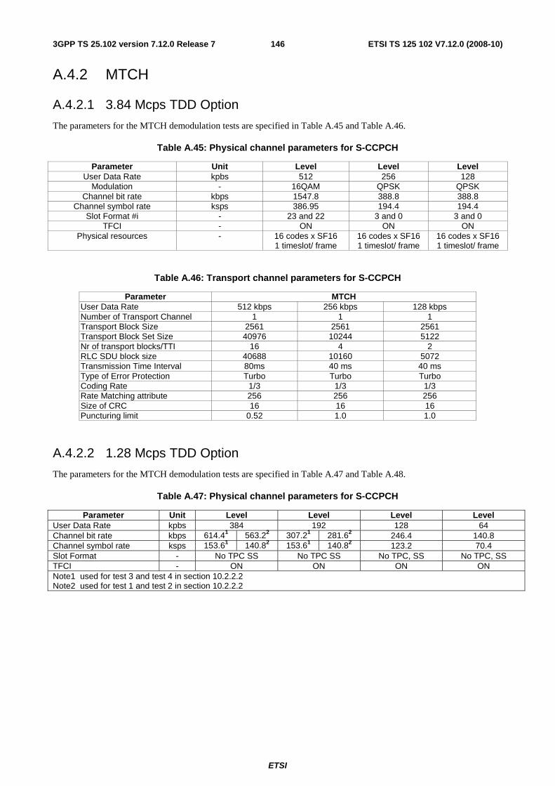
ETSI
ETSI TS 125 102 V7.12.0 (2008-10) 1463GPP TS 25.102 version 7.12.0 Release 7
A.4.2 MTCH
A.4.2.1 3.84 Mcps TDD Option
The parameters for the MTCH demodulation tests are specified in Table A.45 and Table A.46.
Table A.45: Physical channel parameters for S-CCPCH
Parameter Unit Level Level Level User Data Rate kpbs 512 256 128
Modulation - 16QAM QPSK QPSK Channel bit rate kbps 1547.8 388.8 388.8
Channel symbol rate ksps 386.95 194.4 194.4 Slot Format #i - 23 and 22 3 and 0 3 and 0
TFCI - ON ON ON Physical resources - 16 codes x SF16
1 timeslot/ frame 16 codes x SF16 1 timeslot/ frame
16 codes x SF16 1 timeslot/ frame
Table A.46: Transport channel parameters for S-CCPCH
Parameter MTCH User Data Rate 512 kbps 256 kbps 128 kbps Number of Transport Channel 1 1 1 Transport Block Size 2561 2561 2561 Transport Block Set Size 40976 10244 5122 Nr of transport blocks/TTI 16 4 2 RLC SDU block size 40688 10160 5072 Transmission Time Interval 80ms 40 ms 40 ms Type of Error Protection Turbo Turbo Turbo Coding Rate 1/3 1/3 1/3 Rate Matching attribute 256 256 256 Size of CRC 16 16 16 Puncturing limit 0.52 1.0 1.0
A.4.2.2 1.28 Mcps TDD Option
The parameters for the MTCH demodulation tests are specified in Table A.47 and Table A.48.
Table A.47: Physical channel parameters for S-CCPCH
Parameter Unit Level Level Level Level User Data Rate kpbs 384 192 128 64 Channel bit rate kbps 614.41 563.22 307.21 281.62 246.4 140.8 Channel symbol rate ksps 153.61 140.82 153.61 140.82 123.2 70.4 Slot Format - No TPC SS No TPC SS No TPC, SS No TPC, SS TFCI - ON ON ON ON Note1 used for test 3 and test 4 in section 10.2.2.2 Note2 used for test 1 and test 2 in section 10.2.2.2
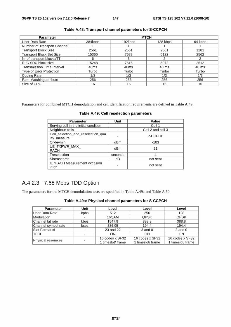
ETSI
ETSI TS 125 102 V7.12.0 (2008-10) 1473GPP TS 25.102 version 7.12.0 Release 7
Table A.48: Transport channel parameters for S-CCPCH
Parameter MTCH User Data Rate 384kbps 192kbps 128 kbps 64 kbps Number of Transport Channel 1 1 1 1 Transport Block Size 2561 2561 2561 1281 Transport Block Set Size 15366 7683 5122 2562 Nr of transport blocks/TTI 6 3 2 2 RLC SDU block size 15248 7616 5072 2512 Transmission Time Interval 40ms 40ms 40 ms 40 ms Type of Error Protection Turbo Turbo Turbo Turbo Coding Rate 1/3 1/3 1/3 1/3 Rate Matching attribute 256 256 256 256 Size of CRC 16 16 16 16
Parameters for combined MTCH demodulation and cell identification requirements are defined in Table A.49.
Table A.49: Cell reselection parameters
Parameter Unit Value Serving cell in the initial condition - Cell 1 Neighbour cells - Cell 2 and cell 3 Cell_selection_and_reselection_quality_measure - P-CCPCH
Qrxlevmin dBm -103 UE_TXPWR_MAX_ RACH dBm 21
Treselection seconds 4 Sintrasearch dB not sent IE "FACH Measurement occasion info"
- not sent
A.4.2.3 7.68 Mcps TDD Option
The parameters for the MTCH demodulation tests are specified in Table A.49a and Table A.50.
Table A.49a: Physical channel parameters for S-CCPCH
Parameter Unit Level Level Level User Data Rate kpbs 512 256 128 Modulation - 16QAM QPSK QPSK Channel bit rate kbps 1547.8 388.8 388.8 Channel symbol rate ksps 386.95 194.4 194.4 Slot Format #i - 23 and 22 3 and 0 3 and 0 TFCI - ON ON ON
Physical resources - 16 codes x SF32 1 timeslot/ frame
16 codes x SF32 1 timeslot/ frame
16 codes x SF32 1 timeslot/ frame

ETSI
ETSI TS 125 102 V7.12.0 (2008-10) 1483GPP TS 25.102 version 7.12.0 Release 7
Table A.50: Transport channel parameters for S-CCPCH
Parameter MTCH User Data Rate 512 kbps 256 kbps 128 kbps Number of Transport Channel 1 1 1 Transport Block Size 2561 2561 2561 Transport Block Set Size 40976 10244 5122 Nr of transport blocks/TTI 16 4 2 RLC SDU block size 40688 10160 5072 Transmission Time Interval 80ms 40 ms 40 ms Type of Error Protection Turbo Turbo Turbo Coding Rate 1/3 1/3 1/3 Rate Matching attribute 256 256 256 Size of CRC 16 16 16 Puncturing limit 0.52 1.0 1.0
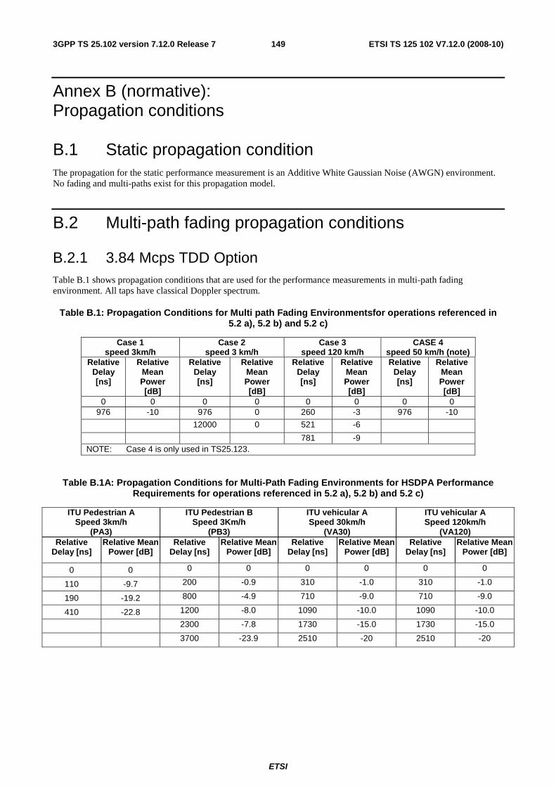
ETSI
ETSI TS 125 102 V7.12.0 (2008-10) 1493GPP TS 25.102 version 7.12.0 Release 7
Annex B (normative): Propagation conditions
B.1 Static propagation condition The propagation for the static performance measurement is an Additive White Gaussian Noise (AWGN) environment. No fading and multi-paths exist for this propagation model.
B.2 Multi-path fading propagation conditions
B.2.1 3.84 Mcps TDD Option Table B.1 shows propagation conditions that are used for the performance measurements in multi-path fading environment. All taps have classical Doppler spectrum.
Table B.1: Propagation Conditions for Multi path Fading Environmentsfor operations referenced in 5.2 a), 5.2 b) and 5.2 c)
Case 1 speed 3km/h
Case 2 speed 3 km/h
Case 3 speed 120 km/h
CASE 4 speed 50 km/h (note)
Relative Delay [ns]
Relative Mean Power [dB]
Relative Delay [ns]
Relative Mean Power [dB]
Relative Delay [ns]
Relative Mean Power [dB]
Relative Delay [ns]
Relative Mean Power [dB]
0 0 0 0 0 0 0 0 976 -10 976 0 260 -3 976 -10
12000 0 521 -6
781 -9 NOTE: Case 4 is only used in TS25.123.
Table B.1A: Propagation Conditions for Multi-Path Fading Environments for HSDPA Performance Requirements for operations referenced in 5.2 a), 5.2 b) and 5.2 c)
ITU Pedestrian A Speed 3km/h
(PA3)
ITU Pedestrian B Speed 3Km/h
(PB3)
ITU vehicular A Speed 30km/h
(VA30)
ITU vehicular A Speed 120km/h
(VA120) Relative
Delay [ns] Relative Mean
Power [dB] Relative
Delay [ns] Relative Mean
Power [dB] Relative
Delay [ns] Relative Mean
Power [dB] Relative
Delay [ns] Relative Mean
Power [dB]
0 0 0 0 0 0 0 0
110 -9.7 200 -0.9 310 -1.0 310 -1.0
190 -19.2 800 -4.9 710 -9.0 710 -9.0
410 -22.8 1200 -8.0 1090 -10.0 1090 -10.0
2300 -7.8 1730 -15.0 1730 -15.0
3700 -23.9 2510 -20 2510 -20

ETSI
ETSI TS 125 102 V7.12.0 (2008-10) 1503GPP TS 25.102 version 7.12.0 Release 7
Table B.1B: Propagation Conditions for Multi path Fading Environments for operations referenced in 5.2 d)
Case 1 speed 2.3km/h
Case 2 speed 2.3 km/h
Case 3 speed 92 km/h
Case 4 speed 38 km/h *
Relative Delay [ns]
Relative Mean Power [dB]
Relative Delay [ns]
Relative Mean Power [dB]
Relative Delay [ns]
Relative Mean Power [dB]
Relative Delay [ns]
Relative Mean Power [dB]
0 0 0 0 0 0 0 0 976 -10 976 0 260 -3 976 -10
12000 0 521 -6 781 -9
NOTE: Case 4 is only used in TS25.123.
Table B.1C: Propagation Conditions for Multi-Path Fading Environments for HSDPA Performance Requirements for operations referenced in 5.2 d)
ITU Pedestrian A Speed 2.3km/h
(PA3)
ITU Pedestrian B Speed 2.3Km/h
(PB3)
ITU vehicular A Speed 23 km/h
(VA30)
ITU vehicular A Speed 92 km/h
(VA120) Relative
Delay [ns] Relative Mean
Power [dB] Relative
Delay [ns] Relative Mean
Power [dB] Relative
Delay [ns] Relative Mean
Power [dB] Relative
Delay [ns] Relative Mean
Power [dB] 0 0 0 0 0 0 0 0
110 -9.7 200 -0.9 310 -1.0 310 -1.0 190 -19.2 800 -4.9 710 -9.0 710 -9.0 410 -22.8 1200 -8.0 1090 -10.0 1090 -10.0
2300 -7.8 1730 -15.0 1730 -15.0 3700 -23.9 2510 -20 2510 -20

ETSI
ETSI TS 125 102 V7.12.0 (2008-10) 1513GPP TS 25.102 version 7.12.0 Release 7
Table B.1D: Propagation Conditions for Multi-Path Fading Environments for MTCH Performance Requirements under an extended delay spread environment
Extended Delay Spread
Operations referenced in 5.2 a), 5.2 b) and 5.2 c)
Speed 3km/h (EDS)
Operations referenced in 5.2 d)
Speed 2.3km/h (EDS)
Relative Delay [ns]
Relative Mean Power [dB]
Relative Delay [ns]
Relative Mean Power [dB]
0 0 0 0
310 -1 310 -1
710 -9 710 -9
1090 -10 1090 -10
1730 -15 1730 -15
2510 -20 2510 -20
12490 -10 12490 -10
12800 -11 12800 -11
13200 -19 13200 -19
13580 -20 13580 -20
14220 -25 14220 -25
15000 -30 15000 -30
27490 -20 27490 -20
27800 -21 27800 -21
28200 -29 28200 -29
28580 -30 28580 -30
29220 -35 29220 -35
30000 -40 30000 -40
B.2.2 1.28 Mcps TDD Option Table B.2 shows propagation conditions that are used for the general performance measurements in multi-path fading environment. Table B.3 shows propagation conditions that are used for HSDPA performance measurements in multi-path fading environments. All taps in both tables have classical Doppler spectrum.
Table B.2: Propagation Conditions for Multi-Path Fading Environments operations referenced in 5.2 a), b) and c)
Case 1, speed 3km/h Case 2, speed 3km/h Case 3, speed 120km/h
Relative Delay [ns]
Relative Mean Power [dB]
Relative Delay [ns]
Relative Mean Power [dB]
Relative Delay [ns]
Relative Mean Power [dB]
0 0 0 0 0 0
2928 -10 2928 0 781 -3
12000 0 1563 -6
2344 -9
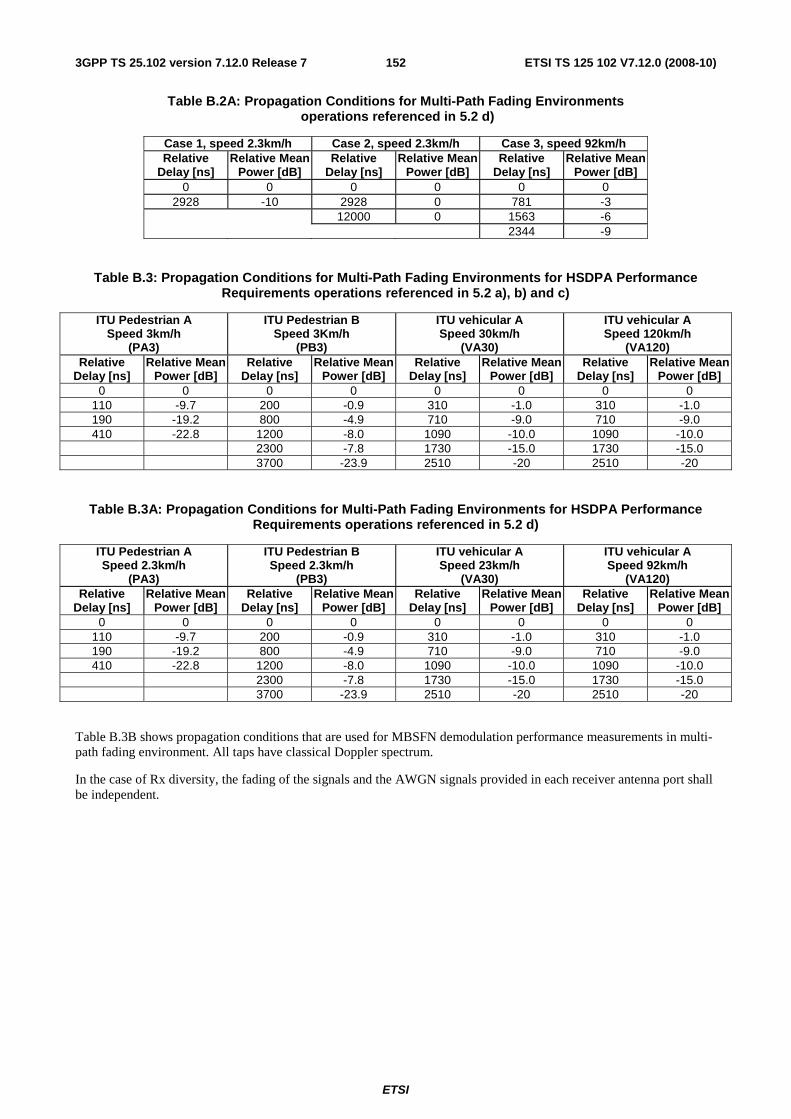
ETSI
ETSI TS 125 102 V7.12.0 (2008-10) 1523GPP TS 25.102 version 7.12.0 Release 7
Table B.2A: Propagation Conditions for Multi-Path Fading Environments operations referenced in 5.2 d)
Case 1, speed 2.3km/h Case 2, speed 2.3km/h Case 3, speed 92km/h Relative
Delay [ns] Relative Mean
Power [dB] Relative
Delay [ns] Relative Mean
Power [dB] Relative
Delay [ns] Relative Mean
Power [dB] 0 0 0 0 0 0
2928 -10 2928 0 781 -3 12000 0 1563 -6 2344 -9
Table B.3: Propagation Conditions for Multi-Path Fading Environments for HSDPA Performance Requirements operations referenced in 5.2 a), b) and c)
ITU Pedestrian A Speed 3km/h
(PA3)
ITU Pedestrian B Speed 3Km/h
(PB3)
ITU vehicular A Speed 30km/h
(VA30)
ITU vehicular A Speed 120km/h
(VA120) Relative
Delay [ns] Relative Mean
Power [dB] Relative
Delay [ns] Relative Mean
Power [dB] Relative
Delay [ns] Relative Mean
Power [dB] Relative
Delay [ns] Relative Mean
Power [dB] 0 0 0 0 0 0 0 0
110 -9.7 200 -0.9 310 -1.0 310 -1.0 190 -19.2 800 -4.9 710 -9.0 710 -9.0 410 -22.8 1200 -8.0 1090 -10.0 1090 -10.0
2300 -7.8 1730 -15.0 1730 -15.0 3700 -23.9 2510 -20 2510 -20
Table B.3A: Propagation Conditions for Multi-Path Fading Environments for HSDPA Performance Requirements operations referenced in 5.2 d)
ITU Pedestrian A Speed 2.3km/h
(PA3)
ITU Pedestrian B Speed 2.3km/h
(PB3)
ITU vehicular A Speed 23km/h
(VA30)
ITU vehicular A Speed 92km/h
(VA120) Relative
Delay [ns] Relative Mean
Power [dB] Relative
Delay [ns] Relative Mean
Power [dB] Relative
Delay [ns] Relative Mean
Power [dB] Relative
Delay [ns] Relative Mean
Power [dB] 0 0 0 0 0 0 0 0
110 -9.7 200 -0.9 310 -1.0 310 -1.0 190 -19.2 800 -4.9 710 -9.0 710 -9.0 410 -22.8 1200 -8.0 1090 -10.0 1090 -10.0
2300 -7.8 1730 -15.0 1730 -15.0 3700 -23.9 2510 -20 2510 -20
Table B.3B shows propagation conditions that are used for MBSFN demodulation performance measurements in multi-path fading environment. All taps have classical Doppler spectrum.
In the case of Rx diversity, the fading of the signals and the AWGN signals provided in each receiver antenna port shall be independent.
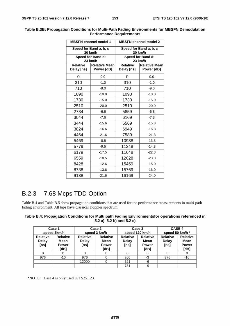
ETSI
ETSI TS 125 102 V7.12.0 (2008-10) 1533GPP TS 25.102 version 7.12.0 Release 7
Table B.3B: Propagation Conditions for Multi-Path Fading Environments for MBSFN Demodulation Performance Requirements
MBSFN channel model 1 MBSFN channel model 2
Speed for Band a, b, c 30 km/h
Speed for Band a, b, c 30 km/h
Speed for Band d: 23 km/h
Speed for Band d: 23 km/h
Relative Delay [ns]
Relative Mean Power [dB]
Relative Delay [ns]
Relative Mean Power [dB]
0 0.0 0 0.0
310 -1.0 310 -1.0
710 -9.0 710 -9.0
1090 -10.0 1090 -10.0
1730 -15.0 1730 -15.0
2510 -20.0 2510 -20.0
2734 -6.6 5859 -6.8
3044 -7.6 6169 -7.8
3444 -15.6 6569 -15.8
3824 -16.6 6949 -16.8
4464 -21.6 7589 -21.8
5469 -8.5 10938 -13.3
5779 -9.5 11248 -14.3
6179 -17.5 11648 -22.3
6559 -18.5 12028 -23.3
8428 -12.6 15459 -15.0
8738 -13.6 15769 -16.0
9138 -21.6 16169 -24.0
B.2.3 7.68 Mcps TDD Option Table B.4 and Table B.5 show propagation conditions that are used for the performance measurements in multi-path fading environment. All taps have classical Doppler spectrum.
Table B.4: Propagation Conditions for Multi path Fading Environmentsfor operations referenced in 5.2 a), 5.2 b) and 5.2 c)
Case 1 speed 3km/h
Case 2 speed 3 km/h
Case 3 speed 120 km/h
CASE 4 speed 50 km/h *
Relative Delay [ns]
Relative Mean Power [dB]
Relative Delay [ns]
Relative Mean Power [dB]
Relative Delay [ns]
Relative Mean Power [dB]
Relative Delay [ns]
Relative Mean Power [dB]
0 0 0 0 0 0 0 0 976 -10 976 0 260 -3 976 -10
12000 0 521 -6 781 -9
*NOTE: Case 4 is only used in TS25.123.

ETSI
ETSI TS 125 102 V7.12.0 (2008-10) 1543GPP TS 25.102 version 7.12.0 Release 7
Table B.5: Propagation Conditions for Multi-Path Fading Environments for HSDPA Performance Requirements for operations referenced in 5.2 a), 5.2 b) and 5.2 c)
ITU Pedestrian A Speed 3km/h
(PA3)
ITU Pedestrian B Speed 3Km/h
(PB3)
ITU vehicular A Speed 30km/h
(VA30)
ITU vehicular A Speed 120km/h
(VA120) Relative
Delay [ns] Relative Mean
Power [dB] Relative
Delay [ns] Relative Mean
Power [dB] Relative
Delay [ns] Relative Mean
Power [dB] Relative
Delay [ns] Relative Mean
Power [dB] 0 0 0 0 0 0 0 0
110 -9.7 200 -0.9 310 -1.0 310 -1.0 190 -19.2 800 -4.9 710 -9.0 710 -9.0 410 -22.8 1200 -8.0 1090 -10.0 1090 -10.0
2300 -7.8 1730 -15.0 1730 -15.0 3700 -23.9 2510 -20 2510 -20
Table B.6: Propagation Conditions for Multi path Fading Environments for operations referenced in 5.2 d)
Case 1 speed 2.3km/h
Case 2 speed 2.3 km/h
Case 3 speed 92 km/h
Case 4 speed 38 km/h *
Relative Delay [ns]
Relative Mean Power [dB]
Relative Delay [ns]
Relative Mean Power [dB]
Relative Delay [ns]
Relative Mean Power [dB]
Relative Delay [ns]
Relative Mean Power [dB]
0 0 0 0 0 0 0 0 976 -10 976 0 260 -3 976 -10
12000 0 521 -6 781 -9
*NOTE: Case 4 is only used in TS 25.123.
Table B.7: Propagation Conditions for Multi-Path Fading Environments for HSDPA Performance Requirements for operations referenced in 5.2 d)
ITU Pedestrian A Speed 2.3km/h
(PA3)
ITU Pedestrian B Speed 2.3Km/h
(PB3)
ITU vehicular A Speed 23 km/h
(VA30)
ITU vehicular A Speed 92 km/h
(VA120) Relative
Delay [ns] Relative Mean
Power [dB] Relative
Delay [ns] Relative Mean
Power [dB] Relative
Delay [ns] Relative Mean
Power [dB] Relative
Delay [ns] Relative Mean
Power [dB] 0 0 0 0 0 0 0 0
110 -9.7 200 -0.9 310 -1.0 310 -1.0 190 -19.2 800 -4.9 710 -9.0 710 -9.0 410 -22.8 1200 -8.0 1090 -10.0 1090 -10.0
2300 -7.8 1730 -15.0 1730 -15.0 3700 -23.9 2510 -20 2510 -20

ETSI
ETSI TS 125 102 V7.12.0 (2008-10) 1553GPP TS 25.102 version 7.12.0 Release 7
Table B.8: Propagation Conditions for Multi-Path Fading Environments for MTCH Performance Requirements under an extended delay spread environment
Extended Delay Spread
Operations referenced in 5.2 a), 5.2 b) and 5.2 c)
Speed 3km/h (EDS)
Operations referenced in 5.2 d)
Speed 2.3km/h (EDS)
Relative Delay [ns]
Relative Mean Power [dB]
Relative Delay [ns]
Relative Mean Power [dB]
0 0 0 0
310 -1 310 -1
710 -9 710 -9
1090 -10 1090 -10
1730 -15 1730 -15
2510 -20 2510 -20
12490 -10 12490 -10
12800 -11 12800 -11
13200 -19 13200 -19
13580 -20 13580 -20
14220 -25 14220 -25
15000 -30 15000 -30
27490 -20 27490 -20
27800 -21 27800 -21
28200 -29 28200 -29
28580 -30 28580 -30
29220 -35 29220 -35
30000 -40 30000 -40

ETSI
ETSI TS 125 102 V7.12.0 (2008-10) 1563GPP TS 25.102 version 7.12.0 Release 7
Annex C (normative): Environmental conditions
C.1 General This normative annex specifies the environmental requirements of the UE. Within these limits the requirements of this specifications shall be fulfilled.
C.2 Environmental requirements for the UE The requirements in this clause apply to all types of UE(s)
C.2.1 Temperature The UE shall fulfil all the requirements in the full temperature range of:
Table C.1
+15°C - +35° C for normal conditions (with relative humidity of 25 % to 75 %);
-10°C - +55°C for extreme conditions (see IEC publications 68-2-1 and 68-2-2)
Outside this temperature range the UE, if powered on, shall not make ineffective use of the radio frequency spectrum. In no case shall the UE exceed the transmitted levels as defined in S25.102 for extreme operation.
C.2.2 Voltage The UE shall fulfil all the requirements in the full voltage range, i.e. the voltage range between the extreme voltages.
The manufacturer shall declare the lower and higher extreme voltages and the approximate shutdown voltage. For the equipment that can be operated from one or more of the power sources listed below, the lower extreme voltage shall not be higher, and the higher extreme voltage shall not be lower than that specified below.
Table C.2
Power source Lower extreme voltage
Higher extreme voltage
Normal conditions voltage
AC mains 0,9 * nominal 1,1 * nominal nominal Regulated lead acid battery 0,9 * nominal 1,3 * nominal 1,1 * nominal Non regulated batteries: Leclanché/lithium Mercury/nickel cadmium
0,85 * nominal 0,90 * nominal
Nominal Nominal
Nominal Nominal
Outside this voltage range the UE if powered on, shall not make ineffective use of the radio frequency spectrum. In no case shall the UE exceed the transmitted levels as defined in S4.01A for extreme operation. In particular, the UE shall inhibit all RF transmissions when the power supply voltage is below the manufacturer declared shutdown voltage.
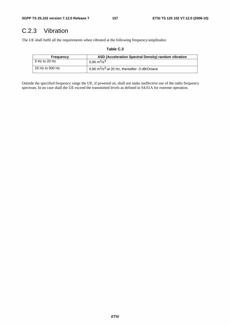
ETSI
ETSI TS 125 102 V7.12.0 (2008-10) 1573GPP TS 25.102 version 7.12.0 Release 7
C.2.3 Vibration The UE shall fulfil all the requirements when vibrated at the following frequency/amplitudes:
Table C.3
Frequency ASD (Acceleration Spectral Density) random vibration 5 Hz to 20 Hz 0,96 m2/s3
20 Hz to 500 Hz 0,96 m2/s3 at 20 Hz, thereafter -3 dB/Octave
Outside the specified frequency range the UE, if powered on, shall not make ineffective use of the radio frequency spectrum. In no case shall the UE exceed the transmitted levels as defined in S4.01A for extreme operation.
ETSI
ETSI TS 125 102 V7.12.0 (2008-10) 1583GPP TS 25.102 version 7.12.0 Release 7
Annex D (informative): Terminal capabilities (TDD) This section provides the UE capabilities related to 25.102.
This section shall be aligned with TS25.306, UE Radio Access Capabilities regarding TDD RF parameters. These RF UE Radio Access capabilities represent options in the UE, that require signalling to the network.
Table D.1 provides the list of UE radio access capability parameters and possible values for 25.102
Table D.1: RF UE Radio Access Capabilities
UE radio access capability parameter
Value range
TDD RF parameters UE power class (25.102 section 6.2.1)
2, 3 NOTE: Only power classes 2 and 3
are part of R99
Radio frequency bands (25.102 section 5.2)
a), b), c), a+b), a+c), b+c, a+b+c)
Chip rate capability (25.102)
3.84 Mcps,1.28 Mcps respectively
ETSI
ETSI TS 125 102 V7.12.0 (2008-10) 1593GPP TS 25.102 version 7.12.0 Release 7
Annex E (informative): Change request history
TSG 29 CR R Title Cat Curr New Work Item RP-29 Rel-7 version created based on v6.2.0 7.0.0 RP-29 RP-050501 0153 Introduction of UMTS 2.6GHz operating band for
TDD B 6.1.0 7.0.0 RInImp-
UMTS2600TDD
RP-29 RP-050501 0154 UMTS 2.6 GHz TDD Propagation Conditions B 6.1.0 7.0.0 RInImp-UMTS2600TDD
RP-29 RP-050501 0155 UMTS 2.6 GHz TDD UE Receiver Specifications B 6.1.0 7.0.0 RInImp-UMTS2600TDD
RP-29 RP-050501 0156 2 Channel Raster and UARFCN for 3.84 Mcps TDD in UMTS 2.6 GHz
B 6.1.0 7.0.0 RInImp-UMTS2600TDD
RP-29 RP-050501 0157 Introduction of UMTS 2.6 GHz new operating band for 1.28Mcps TDD
B 6.1.0 7.0.0 RInImp-UMTS2600TDD
RP-29 RP-050501 0158 Introduction of Propagation Conditions for UMTS 2.6 GHz for 1.28Mcps TDD
B 6.1.0 7.0.0 RInImp-UMTS2600TDD
RP-29 RP-050501 0159 Introduction of UMTS 2.6 GHz requirements for blocking and spurious emission of UE receiver for 1.28Mcps TDD
B 6.1.0 7.0.0 RInImp-UMTS2600TDD
RP-30 RP-050740 0160 1 Additional UE Tx Spurious Emission for co-existence with 2.6 GHz FDD
B 7.0.0 7.1.0 RInImp-UMTS2600TDD
RP-31 RP-060104 0162 1 Modifications to HSDPA test parameters for 1.28Mcps TDD
A 7.1.0 7.2.0 TEI6
RP-31 RP-060113 0163 1 MBMS Requirements for MCCH & MTCH channels B 7.1.0 7.2.0 MBMS-RAN-RF-TDD
RP-32 RP-060313 0165 2 1.28Mcps TDD MBMS UE performance requirements
B 7.2.0 7.3.0 MBMS-RAN-RF-TDD
RP-32 RP-060309 0166 1 7.68 Mcps Frequency Band & Channel Arrangement B 7.2.0 7.3.0 VHCRTDD-RF
RP-32 RP-060309 0167 2 7.68 Mcps UE Transmitter Characteristics B 7.2.0 7.3.0 VHCRTDD-RF
RP-32 RP-060309 0168 7.68 Mcps UE Receiver Characteristics B 7.2.0 7.3.0 VHCRTDD-RF
RP-32 RP-060309 0169 7.68 Mcps - Channel Performance B 7.2.0 7.3.0 VHCRTDD-RF
RP-32 RP-060309 0170 1 7.68 Mcps Measurement Channels & Propagation Conditions
B 7.2.0 7.3.0 VHCRTDD-RF
RP-33 RP-060522 0180 HS-SCCH performance requirement for 3.84 Mcps TDD option and 7.68 Mcps TDD option
7.3.0 7.4.0 TEI7
RP-33 RP-060516 0185 1 Out of band blocking for 3.84 Mcps and 7.68 Mcps TDD UE operating in 2010-2025 MHz of band (a) in Japan.
7.3.0 7.4.0 TEI7
RP-33 RP-060517 0190 Clarification of Tx spurious emission level from 3.84 Mcps and 7.68 MCps TDD UE into PHS band
7.3.0 7.4.0 TEI7
RP-33 RP-060529 0192 Editorial corrections to 3.84 Mcps TDD UE performances on MBMS.
7.3.0 7.4.0 TEI7
RP-33 RP-060528 0193 Performance requirements for 3.84 Mcps E-DCH associated downlink signalling channels: E-AGCH and E-HICH
7.3.0 7.4.0 TEI7
RP-33 RP-060526 0194 7.68 Mcps Operations in 2.6 GHz band 7.3.0 7.4.0 TEI7 RP-33 RP-060530 0195 Clarification of 7.68 Mcps TDD UE ACLR at +/- 10
MHz offset. 7.3.0 7.4.0 MBMS-RAN-
RF-TDD

ETSI
ETSI TS 125 102 V7.12.0 (2008-10) 1603GPP TS 25.102 version 7.12.0 Release 7
RP-33 RP-060530 0196 Performance requirements for 3.84 Mcps E-DCH associated downlink signalling channels: E-AGCH and E-HICH
7.3.0 7.4.0 EDCHTDD-RF
RP-34 RP-060810 0200 Combined MBMS demodulation and Cell identification requirement for 1.28 Mcps TDD
A 7.4.0 7.5.0 TEI6
RP-34 RP-060818 0198 Performance requirements for 7.68 Mcps E-DCH associated downlink signalling channels: E-AGCH and E-HICH
B 7.4.0 7.5.0 TEI7
RP-34 RP-060816 0197 PLCCH Performance Requirement B 7.4.0 7.5.0 RANimp-RABSE-CodOptLCRTDD
RP-35 RP-070081 0209 Modificaiton to SEM for 1.28Mcps TDD A 7.5.0 7.6.0 TEI4 RP-35 RP-070082 0201 Performance requirements for 7.68 Mcps E-DCH
associated downlink signalling channels: E-AGCH and E-HICH
B 7.5.0 7.6.0 TEI7
RP-35 RP-070082 0203 Corrections & clarifications on 7.68 Mcps TDD MTCH demodulation test case.
F 7.5.0 7.6.0 TEI7
RP-35 RP-070085 0202 Performance requirements for MTCH using 16QAM in an extended delay spread environment
B 7.5.0 7.6.0 MBMSE-RANPhysTDD
RP-35 RP-070085 0211 Performance requirement for MCCH in an extended delay spread environment
B 7.5.0 7.6.0 MBMSE-RANPhysTDD
RP-36 RP-070376 0225 Performance requirements for MCCH in an extended delay spread environment.
F 7.6.0 7.7.0 MBMSE-RANPhysTDD
RP-36 RP-070376 0212 1 MCCH & MTCH Channels Performances in TDD MBSFN
B 7.6.0 7.7.0 MBMSE-RANPhysTDD
RP-36 RP-070376 0224 1 Performance requirements for MTCH using 16QAM in an extended delay spread environment.
F 7.6.0 7.7.0 MBMSE-RANPhysTDD
RP-36 RP-070376 0213 1 Performance requirement for MTCH in a MBSFN TDD UE sharing the same platform with a FDD UE
B 7.6.0 7.7.0 MBMSE-RANPhysTDD
RP-36 RP-070377 0223 1 Performance requirements for 1.28 Mcps E-DCH associated downlink signalling channels: E-AGCH and E-HICH
B 7.6.0 7.7.0 LCRTDD-EDCH-RF
RP-36 RP-070373 0222 1 Updating of HSDPA demodulation performance requirements for 1.28Mcps TDD
A 7.6.0 7.7.0 TEI7
RP-36 RP-070373 0216 Updating of HSDPA demodulation performance requirements for 1.28Mcps TDD-FRC
A 7.6.0 7.7.0 TEI7
RP-36 RP-070373 0219 Updating of HSDPA demodulation performance requirements for 1.28Mcps TDD-VRC
A 7.6.0 7.7.0 TEI7
RP-37 RP-070651 0243 Change to HSDPA for 1.28 Mcps TDD F 7.7.0 7.8.0 TEI7 RP-37 RP-070651 0240 Correction of UE maximum output power classes for
1.28 Mcps TDD option F 7.7.0 7.8.0 TEI7
RP-37 RP-070651 0230 Inclusion of 7.68 Mcps in the scope of document D 7.7.0 7.8.0 TEI7 RP-37 RP-070651 0232 Clarification of MBMS test for LCR TDD A 7.7.0 7.8.0 TEI7 RP-37 RP-070652 0229 Requirements for maximum Input level for HS-
PDSCH reception A 7.7.0 7.8.0 TEI7
RP-37 RP-070654 0234 Performance Requirements for TDD MBSFN Channels
B 7.7.0 7.8.0 MBMSE-RANPhysTDD
RP-38 RP-070935 0244 LCR TDD MBSFN UE demodulation performance requirements
B 7.8.0 7.9.0 MBMSE-RANPhysLCRTDD
RP-38 RP-070937 0245 Relative delay corrections in Extended Delay Spread propagation condition
F 7.8.0 7.9.0 TEI7
RP-39 RP-080118 0250 Adding EVM requirement for UL 16QAM F 7.9.0 7.10.0 LCRTDD-EDCH-RF
RP-39 RP-080118 0251 1 Adding requirements for MBSFN capable UE (dedicated carrier case)
F 7.9.0 7.10.0 MBMS-RANPhysLCRTDD
RP-39 RP-080119 0246 Omissions of minimum requirements for blocking characteristics
F 7.9.0 7.10.0 TEI6
ETSI
ETSI TS 125 102 V7.12.0 (2008-10) 1613GPP TS 25.102 version 7.12.0 Release 7
RP-39 RP-080119 0249 Deleting redundant notes for receiver spurious emissions
F 7.9.0 7.10.0 TEI6
RP-40 RP-080324 0263 Clarification of MCCH Physical Channel for MBSFN F 7.10.0 7.11.0 MBMSE-RANPhysTDD
RP-40 RP-080324 0262 Correction to MTCH parameters for demodulation test in TDD MBSFN
F 7.10.0 7.11.0 MBMSE-RANPhysTDD
RP-40 RP-080324 0257 Corrections for LCR TDD MBMS F 7.10.0 7.11.0 MBMSE-RANPhysTDD
RP-40 RP-080324 0256 MBSFN Reference Channel F 7.10.0 7.11.0 MBMSE-RANPhysTDD
RP-41 RP-080628 0268 RF requirements in later releases A 7.11.0 7.12.0 RInImp8-UMTS2300TDD
ETSI
ETSI TS 125 102 V7.12.0 (2008-10) 1623GPP TS 25.102 version 7.12.0 Release 7
History
Document history
V7.1.0 December 2005 Publication
V7.2.0 March 2006 Publication
V7.3.0 June 2006 Publication
V7.4.0 October 2006 Publication
V7.5.0 December 2006 Publication
V7.6.0 March 2007 Publication
V7.7.0 June 2007 Publication
V7.8.0 October 2007 Publication
V7.9.0 January 2008 Publication
V7.10.0 April 2008 Publication
V7.11.0 June 2008 Publication
V7.12.0 October 2008 Publication