trizeps v module - keith & koep
TRANSCRIPT
Keith & Koep GmbH
Confidential Information
Trizeps V Module (Vers. 0.7, Feb. 2015)
1.0 Introduction
The Trizeps V Module is based on the Intel/Marvell® XScale™ Core CPU PXA320 (806) ARM® Architecture v.5TE compliant and application code compa-tible with Intel® SA-1110 and PXA2XX processor which are used on the Trizeps-I, Trizeps II and Trizeps III and Trizeps-IV XX Modules. The CPU is based on Intel/Marvell® Superpipelined RISC technology for high core speeds at low power (1.5 Mio Dhrystone 2.1 per second @ 806 MHz). It includes Intel/Marvell® wire-less MMX® technology, enabling high performance, low-power multimedia accele-ration with a general-purpose instruction set. Intel/Marvell® Quick Capture technology provides one of the industry´s most flexible and powerful camera inter-faces for capturing digital images and video. While performance is key, power con-sumption is also a critical component. The new capabilities of the wireless SpeedStep® technology provide a quantum leap forward in low-power operation.Some features of the PXA320: Integrated memory and PCMCIA/CompactFlash Controller with 133 MHz Memory Bus (DDR). System Control Module includes general-purpose interruptible I/O ports, real-time clock, watchdog and interval timers, power management controller, interrupt and reset controller, LCD controller and two on-chip oscillators. Trizeps V includes also the Wolfson WM9715L, on a single chip it combines audio codec functions, a touch-screen controller and power management interfaces. The incorporated A/D converter and the touch screen inter-face provides complete control and read-out of a 4 wire resistive touch screen.
Features of Trizeps V
Marvell XScale PXA320 806 MHz WM9715L codec with Audio and Touch
16 Bit Intel Strata Flash 32/64MB DM9000 10/100MBit Ethernet-Controller
NAND-flash Option High-Eff. switching core-voltage regula-tor supporting SpeedStep® Features
32 Bit LP DDR-RAM (128 MB or 256MB) Demux Circuit to keep comatibility to for-mer Trizeps Modules
Reset Generator Pin compatible to TRIZEPS III / IV
1 von 17

Keith & Koep GmbH
2.0 Functional description of the Trizeps V Module
In the following you’ll find special information about the Trizeps V Module. For more information concerning the PXA320, WM9715L or Ethernet peripherals ple-ase refer to the manufacturers original manuals:
PXA320 http://marvell.comBGW211 http://www.philips.comWM9715L http://www.wolfsonmicro.com
Figure 1. Trizeps IV-WL Module
Components of the Trizeps V Module:
1. Intel® XScale PXA320 (microprocessor)
2. WM9715L (a single chip, stereo audio codec equipped with touch screen and power management interfaces ), IRQ GP01
3. DDR-RAM 32-Bit wide @ bank 0
4. Flash: Intel Strata® Flash (J3 or P30,P33) 16-Bit wide @ nCS0
5. Optional: NAND Flash Option
6. Davicom DM9000 Ethernet controller
7. Switching-mode core voltage regulator with I2C management interface
8. USB 2.0 Phy. for USB function Interface
9. uSD Socket, 2nd SDIO Interfca (also wired to SODIMM)
10.Reset generator
2.1 Interfaces of the XScale PXA320 on SODIMM socket
The Trizeps V Module offers the following interfaces:
2.1.1 Universal Asynchronous Receiver / Transmitter (UART) serial ports
The XScale PXA320 processor has 3 UARTs: Full Function UART (FFUART), Bluetooth UART (BTUART), and Standard UART (STUART).
The UARTs share the following features:
XScale
CodecWM9715L
Reset Ethernet
Reset In
4wire-Touch
Headphone Output
Mic/Line Input// 32
ADRDATA
PXA320
//Speedstep
Nor-Flash
16/CS1
EEProm
DDR-Ram
Demux
NAND opt.
USB 2.0Phy
uSD-Socket
Regulators
Confidential Information Trizeps V Module (Vers. 0.7, Feb. 2015) 2 von 17

Keith & Koep GmbH
• Functionally compatible with the 16550
• Ability to add or delete standard asynchronous communications bits (start, stop and parity) in the serial data
• Independently controlled transmit, receive, line status, and data set interrupts
• Programmable baud rate generator that allows the internal clock to be divided by
1 to (216-1) to generate an internal 16X clock
• Modem control pins that allow flow control through software
Full Function UART: All of the modem signals are accessible on the SODIMM socket.
Bluetooth UART: The signals TxD, RxD, CTS and RTS are accessible on the SODIMM socket.
Standard UART: The signals IRRxD and IRTxD are accessible on the SODIMM socket. This serial port can work as Fast Infrared Communications Port (FICP). It operates at half-duplex and provides direct connection to commercially available Infrared Data Association (IrDA) compliant LED transceivers. The FICP is based on the 4-Mbps IrDA standard and uses four-position pulse modulation (4PPM) and a specialized serial packet protocol developed for IrDA transmission. To support the standard, the FICP has:
• A bit Encoder / Decoder
• A serial-to-parallel data engine
• A transmit FIFO 128 entries deep and 8 bits wide
• A receive FIFO 128 entries deep and 11 bits wideThe FICP shares GPIO pins for transmit and receive data with the Standard UART. Only one of the ports can be used at a time.
2.1.2 Universal Serial Bus (USB) 2.0 Device Controller (U2D)
The U2D supports 8 endpoints and can operate half-duplex at a rate of 12Mbps ( Full Speed) or 480Mbps (High Speed) .
2.1.3 Universal Serial Bus (USB) Host and OTG-Controller
The PXA320 has one dedicated USB Host Port and one USB OTG Port. The OTG-port can function as host or device-port. Both host-ports support Full Speed and Low Speed. The device-port supports Full Speed only.
2.1.4 I²C Bus Interface Unit
The I²C bus was created by the Phillips Corporation and is a serial bus with a two-pin interface. The SDA data pin is used for input and output functions and the SCL clock pin is used to control and reference the I²C bus. The I²C bus unit allows the PXA320 to serve as a master and slave device that resides on the I²C bus.
The I²C unit enables the PXA320 to communicate with I²C peripherals and micro-controllers for system management functions. The I²C bus requires a minimum amount of hardware to relay status and reliability information concerning the PXA320 subsystem to an external device.
The I²C unit is a peripheral device that resides on the PXA320 internal bus. Data is transmitted to and received from the I²C bus via a buffered interface. Control and status information is relayed through a set of memory-mapped registers. Refer to The I²C-Bus Specification for complete details on I²C bus operation.
Confidential Information Trizeps V Module (Vers. 0.7, Feb. 2015) 3 von 17

Keith & Koep GmbH
2.1.5 MultiMediaCard / SD/SDIO-Card Controller
The PXA320 supports 2 Multimedia-Card and SDCard Controllers.
The MMC/SD/SDIO controllers act as a link between the software that accesses the PXA320 processor and the MMC stack (a set of memory cards) and supports Multi-media Card, Secure Digital, and Secure Digital I/O communications protocols. The MMC controller supports the MMC system, a low-cost data storage and communi-cations system. The MMC controller in the PXA320 processor is based on the stan-dards outlined in the MultiMediaCard System Specification Version 3.2. The SD controller supports one SD or SDIO card based on the standards outlined in the SD Memory Card Specification Version 1.01 and SDIO Card Specification Version 1.0 (Draft 4).The MMC controller features:
• Data-transfer rates up to 19.5 Mbps for MMC, 1-bit SD/SDIO, and SPI mode data transfers
• Data-transfer rates up to 78 Mbps for 4-bit SD/SDIO data transfers
• Two modes of operation: MMC/SD/SDIO mode and SPI mode. MMC/SD/SDIO mode supports MMC, SD, and SDIO communications protocols. SPI mode sup-ports the SPI communications protocol.
• 1- and 4-bit data transfers are supported for SD and SDIO communications pro-tocols.
• Support for all valid MMC and SD/SDIO protocol data-transfer modes
• Using the MMC communications protocol, multiple MMC cards are supported.
• Using the SD or SDIO communications protocol, one SD or SDIO card per slot is supported.
2.2 Codec (WM9715L)
Trizeps-V includes the Wolfson WM9715L. It integrates an AC ’97 Rev. 2.2 inter-face for communication to Intel® XScale processor.
If you need a detailed description please refer to Wolfsons datasheet. For interrupt programming of the codec use GP15 (IRQ). GP15 is a general purpose input/output of the PXA320. The interrupt line is also connected to the processors EXT_Wakeup1 Pin.
Features of the WM9715L:
• Integrated AC ’97 Rev. 2.2 interface.
• 18-bit stereo audio codec with Variable Rate Audio, input and output gain, digital sound processing, capable of driving headphones, and connecting to microphone and line level inputs.
• 4-wire resistive touch screen interface circuit supporting position, pressure and plate resistance measurements.
• 12-bit successive approximation ADC with internal track-and-hold circuit and analog multiplexer for touch screen readout and monitoring of four external (3.3 V) sources.
• 3.3 V supply voltage and two comparator inputs for battery monitoring.
Confidential Information Trizeps V Module (Vers. 0.7, Feb. 2015) 4 von 17

Keith & Koep GmbH
2.3 Memory
The XScale PXA230 offers four different memory spaces: DDR-RAM, internal SRAM, Static Memory and Card Memory.
2.3.1 DDR-RAM interfaceThe PXA2320 Memory Controller supports two chip-selects of SDRAM. Each chip-select can address up to 1 GByte of memory. It supports Jedec compliant DDR SDRAMs with autopowerdown and selfrefresh support. It provides a robus DDR-strobe calibration scheme for hardware calibration and programming. It supports dynamic resistive Compensation (Rcomp) circuits that can change output pad drive-strenght and slew rate. The Trizeps V uses the first chip select of two and 32 data-lines. Currently options for 128 and 256 MByte of mobile DDR-RAM are avail-lable.
2.3.2 Internal SRAM
The PXA320 has 768kByte of internal SRAM.
2.3.3 Data Flash interface / Variable Latency I/O interface
The Trizeps-V NOR Flash memory is selected by the first (CS2 GPIO3) of the 2 chip selects and uses 16 data-lines. Usually the size of Flash memory is 32 MByte. Trizeps-V uses a Demux Circuit to generate a Trizeps-III/IV compatible bus inter-face. \CS_3 (GPIO04 ) is divided into 4 subselects using ADR 24 and ADR 23. Here you can see a truth table for internal external addressing:
2.3.4 NAND Flash Memory
Trizeps -V has a NAND flash mounting option. NAND is mounted 8 bit wide to DF_CS0.
2.4 16-Bit PC Card / Compact Flash Interface
The PXA320 card interface is based on The PC Card Standard - Volume 2 - Electri-cal Specification, Release 2.1, and CF+ and CompactFlash Specification Revision 1.4. The 16-bit PC Card / Compact Flash interface provides control signals to sup-port any combination of 16-bit PC Card / Compact Flash for two card sockets, using address line (A[11:0]) and data lines (D[15:0]).
The PXA320 16-bit PC Card / Compact Flash Controller provides the following signals:
• PREG
• POE and PWE allow memory and attributes reads and writes
• PIOR, PIOW and PIOIS16 control I/O reads and writes
• PWAIT allows extended access times
TABLE 1.
A24 A23 Select
1 1 DM9000 internal Ethernet Controller
1 0 CSX_4 SODIMM Pin 106
0 1 CSX_1 SODIMM Pin 105
0 0 CSX_3 SODIMM Pin 107
Confidential Information Trizeps V Module (Vers. 0.7, Feb. 2015) 5 von 17

Keith & Koep GmbH
• PCE2 and PCE1 are byte select high and low for a 16-bit data bus
• PSKTSEL selects between two card sockets
Keith & Koep GmbH uses a small external logic to switch the power to the cardin-terface and drive external buffers, which are needed to build a hotplug save system. There is also a buffer to read status signals like the BVDDx and VSx signals. Using the reference schematics, you can be sure to be compatible with Keith&Koep’s bootloader and OS adaptions. Note that CF-PCMCIA standard seem to disappear from current designs. The PXA320 seems to read the \PIOIS16 signal in a critical time. You should expect timing issues with 16-Bit accesses.
2.5 Voltage converter
The Trizeps IV-WL Module uses a single power supply of +3V3. To generate the different voltages needed for the PXA320 a highly integrated power supply system with a high efficiency switch-mode voltage converter is used. The core voltage can
be adjusted dynamically through a dedicated I2C interface.
2.6 Reset generator
Resetting the board is possible by using the RESET_IN input or by using the JTAG Reset Input.
2.7 JTAG / Debug Port
The JTAG / Debug port consists of several shift registers, with the destination con-trolled by the TMS pin and data I/O with TDI / TDO. The JTAG / Debug port provi-des two different functionalities:
• Programming Flash memory by pushing data through the shift registers
• Hardware-testing using boundary scan interface according to IEEE 1149.1
Confidential Information Trizeps V Module (Vers. 0.7, Feb. 2015) 6 von 17

Keith & Koep GmbH
3.0 Firmware / Bootloader:
The Trizeps V is delivered with a bootloader which offers an easy way to install or update an operating system by using the serial interface, ehternet, SD-Card or Compact Flash. For more informations refer to the „bootloader3.pdf“ on the Evalu-ation Kit CD-ROM or contact Keith & Koep.
4.0 DC operating conditions
1. Supply voltage 3.3 V
2. Typical operating current @806MHz, 128MB DDR-RAM
Running 530 mA (No USB) tbd.
Idle 270 mA (No USB) tbd.
Suspend tbd.
5.0 Ordering Information
Ordercode:
35120 Trizeps V/C806/R128/P33.32.1BF/ETH/CODW/RoHS
Explanation:
Trizeps-V, 806Mhz, 128MB RAM, 32MB Flash, EthernetWolfson Codec
For further ordering information please contact Keith & Koep.
Confidential Information Trizeps V Module (Vers. 0.7, Feb. 2015) 7 von 17

Keith & Koep GmbH
6.0 Pinout information and description
All of the significant signals are accessible via the 200-pin SODIMM socket.
TABLE 2. Pinout information of the connector J2 of the Trizeps V Module (200-pin SODIMM-socket)
Pin Name Description
1 MIC_OUT microphone input signal (WM9715L)
2 AD3 analog voltage input (WM9715L)a
3 MIC_GND microphone ground switch input (WM9715L)
4 VIN_AD2 analog voltage input (WM9715L)a
5 LINEIN_L Line in left channel (WM9715L)
6 AD1 analog voltage input (WM9715L)a
7 LINEIN_R Line in right channel (WM9715L)
8 VBAT_AD0 analog voltage input (WM9715L)a
9 VSSA_AUDIO Analog ground audio (WM9715L) do not leave open
10 VDDA_AUDIO Analog power audio (WM9715L) do not leave open
11 VSSA_AUDIO Analog ground audio (WM9715L) do not leave open
12 VDDA_AUDIO Analog power audio (WM9715L) do not leave open
13 HEADPHONE_GND Line out ground output (WM9715L)
Note: 1.75 V DC out. Do not connect to GND !
14 TSPX positive X-plate touch screen (WM9715L)b
15 HEADPHONE_L Line out left channel (WM9715L)
16 TSMX negative X-plate touch screen (WM9715L)c
17 HEAPHONE_R Line out right channel (WM9715L)
18 TSPY positive Y-plate touch screen (WM9715L)d
19 COM3_RXD serial port 3 receive pin (IrDA) (PXA 320, GP30[2])
20 TSMY negative Y-plate touch screen (WM9715L)e
21 COM3_TXD serial port 3 transmit pin (IrDA) (PXA 320,GP31[2])
22 VDD_FAULT Main power source goes out of regulation (PXA 320)
23 COM1_DTR Full Function UART DTR (PXA320, GP81)
24 BATT_FAULT Main battery is low or removed (PXA320)
25 COM1_CTS Full Function UART Clear To Send (PXA320,GP77[1])
26 RESET_IN reset input
27 COM1_RTS Full Function UART Ready To Send (PXA320,GP82[1])
28 TUDC- USB Fn bidirectional (U2D) (PXA320, USBC_N)
29 COM1_DSR Full Function UART Data Set Ready (PXA320, GP79[1])
30 TUDC+ USB Fn bidirectional (U2D) (PXA320, USBC_P)
31 COM1_DCD Full Function UART DCD (PXA320, GP78[1])
32 COM2_CTS BlueTooth UART Clear To Send (PXA320, GP112)
33 COM1_RXD Full Function UART Receive Data (PXA320, GP75[1])
34 COM2_RTS BlueTooth UART Ready To Send (PXA320, GP109)
Confidential Information Trizeps V Module (Vers. 0.7, Feb. 2015) 8 von 17

Keith & Koep GmbH
35 COM1_TXD Full Function UART Transmit Data (PXA320, GP76[1])
36 COM2_RXD BlueTooth UART Receive Data (PXA320,GP110)
37 COM1_RI Full Function UART Ring Indicator (PXA320, GP80[1])
38 COM2_TXD BlueTooth UART Transmit Data (PXA320, GP111)
39 GND Ground
40 +3V3 Power Supply
41 GND Ground
42 +3V3 Power Supply
43 GPIO09_IRQ_PIC General purpose I/O (PXA320,GP09)
Also wired to National LP3971
44 L_BIAS LCD controller display data (PXA320,GP17_2)
45 GPIO16_PRDY General purpose I/O (PXA320,GP16)
46 LDD07 LCD controller display data (PXA32,GP13_2)
47 MMC_CLK General purpose I/O (PXA320,GP22[4])
48 LDD09 LCD controller display data (PXA320,GP64)
49 CIF_DD0 General purpose I/O (PXA320,GP49[1])
50 LDD11 LCD controller display data (PXA320,GP66)
51 MMC_DAT3 General purpose I/O (PXA320,GP21[4])
52 LDD12 LCD controller display data (PXA320,GP67)
53 CIF_DD1 General purpose I/O (PXA320,GP50[1])
54 LDD13 LCD controller display data (PXA320,GP68)
55 GPIO113_IRQUSB_SL General purpose I/O (PXA320,GP113)
56 L_PCLK LCD pixel clock (PXA320,GP16_2)
57 CIF_DD2 General purpose I/O (PXA320,GP51[1])
58 LDD03 LCD controller display data (PXA320,GP9_2)
59 MMC_DET (act.Hi) General purpose I/O (PXA320,GP114)
60 LDD02 LCD controller display data (PXA320,GP8_2)
61 CIF_DD3 General purpose I/O (PXA320,GP52_1)
62 LDD08 LCD controller display data (PXA320,GP63)
63 CIF_DD4 General purpose I/O (PXA320,GP53[1])
64 LDD15 LCD controller display data (PXA320,GP70)
65 CIF_DD5 General purpose I/O (PXA320,GP54[1],GP11)
66 LDD14 LCD controller display data (PXA320,GP69)
67 CIF_DD6/PWM1 General purpose I/O (PXA320,GP55[1],GP12)
68 L_LCLK LCD line clock (PXA320,GP15_2)
69 IRQ_HIL, PWM2, CHOUT0
General purpose I/O (PXA320,GP13)
70 LDD01 LCD controller display data (PXA320,GP7_2)
71 CIF_DD7 TTLIO_IRQ General purpose I/O (PXA320,GP56[0],GP84)
TABLE 2. Pinout information of the connector J2 of the Trizeps V Module (200-pin SODIMM-socket)
Pin Name Description
Confidential Information Trizeps V Module (Vers. 0.7, Feb. 2015) 9 von 17
Keith & Koep GmbH
72 LDD05 LCD controller display data (PXA320,GP11_2)
73 CIF_DD8 General purpose I/O (PXA320,GP57[1])
74 LDD10 LCD controller display data (PXA320,GP65)
75 CIF_DD9 General purpose I/O (PXA320,GP58[1])
76 LDD00 LCD controller display data (PXA320,GP6_2)
77 PCD PCMCIA Card Detect General purpose I/O (PXA320,GP17)
78 LDD04 LCD controller display data (PXA320,GP10_2)
79 GPIO14_POWERFAIL
PWM3, CHOUT1, HZ_CLK,
ONE_WIRE
General purpose I/O (PXA320,GP14)
GP14[1]
GP14[4,6]
GP14[5]
80 LDD06 LCD controller display data (PXA320,GP12_2)
81 MMCDAT1 General purpose I/O (PXA320,GP19[4])
82 L_FCLK LCD frame clock (PXA320,GP14_2)
83 GND Ground
84 +3V3 Power Supply
85 MMCDAT2 General purpose I/O (PXA320,GP20)
86 CIF_FV
SSP_FRM4
PXA320,GP62[0]
GP94[1]
87 RESET_OUT Reset output (PXA320)
88 CIF_MCLK
SSP_CLK4
(PXA320,GP59[0])
GP93[1]
89 WE Memory Write Enable (PXA320, DF_ALE_WE1)
90 CIF_PCLK
SSP_CLK4
PXA320,GP60[0]
GP96[1]
91 OE Memory Output Enable (PXA320, D_CLW_OE)
92 CIF_LV
SSP_TXD4
(PXA320,GP61[1])
GP95[1]
93 RD/WR read/write direction control for memory bus (mux bus PXA320)
94 PCE1 PCMCIA card enable (low-byte) (mux bus PXA320)
95 RDY General purpose I/O (PXA320, GP2)
96 PCE2 PCMCIA card enable (high-byte) (mux bus PXA320)
97 POE PCMCIA output enable (PXA320,DF_OE)
(mounting option GP120)
98 PREG PCMCIA register select (mux bus PXA320)
99 PWE PCMCIA write enable, (PXA320, DF_WE)
(mounting option GP119)
TABLE 2. Pinout information of the connector J2 of the Trizeps V Module (200-pin SODIMM-socket)
Pin Name Description
Confidential Information Trizeps V Module (Vers. 0.7, Feb. 2015) 10 von 17

Keith & Koep GmbH
100 PSKTSEL PCMCIA socket select (PXA320, nPXCVREN)
(mounting option GP124)
101 PIOW PCMCIA I/O write (PXA320,GP6)
102 PWAIT PCMCIA wait (PXA320,GP8)
103 PIOR PCMCIA I/O read (PXA320,GP5)
104 PIOIS16 I/O select 16 (PXA320,GP7)
105 CS1 static chip select (PXA320, demux sel)
106 CS4 static chip select (PXA320, demux sel)
107 CS3 static chip select (PXA320, demux sel)
108 +3V3 Power Supply
109 GND Ground
110 A08 memory address bus (PXA320)
111 A00 memory address bus (PXA320)
112 A09 memory address bus (PXA320)
113 A01 memory address bus (PXA320)
114 A10 memory address bus (PXA320)
115 A02 memory address bus (PXA320)
116 A11 memory address bus (PXA320)
117 A03 memory address bus (PXA320)
118 A12 memory address bus (PXA320)
119 A04 memory address bus (PXA320)
120 A13 memory address bus (PXA320)
121 A05 memory address bus (PXA320)
122 A14 memory address bus (PXA320)
123 A06 memory address bus (PXA320)
124 A15 memory address bus (PXA320)
125 A07 memory address bus (PXA320)
126 DQM0 PXA320 BE0
127 USBHPEN2 Turn on/off the external Vbus (PXA320 GP115)
128 DQM1 PXA320, BE1
129 USBHPEN1 Turn on/off the Power OTG (PXA320 GP2_2)
130 DQM2 PXA320 GP121
131 USBHPWR1 Overcurrent detect in PXA320 GP2_3
132 DQM3 PXA320,GP122
133 USBHPWR2 Vbus pulsing control (PXA320 GP116)
134 A25 memory address bus (PXA320, !! A20 !!)
135 OTG_VBUS Not Connected
136 A24 memory address bus (PXA320, !! A19 !!)
TABLE 2. Pinout information of the connector J2 of the Trizeps V Module (200-pin SODIMM-socket)
Pin Name Description
Confidential Information Trizeps V Module (Vers. 0.7, Feb. 2015) 11 von 17
Keith & Koep GmbH
137 OTG_ID Connected to the ID pin of the Mini-AB connector for OTG applications (PXA320, GP117)
138 A23 memory address bus (PXA320, !! A18 !!)
139 USBH_P2 Data line for port 2
140 A22 memory address bus (PXA320)
141 USBH_N2 Data line for port 2
142 A21 memory address bus (PXA320)
143 USBH_P1 Data line for port 1
144 A20 memory address bus (PXA320)
145 USBH_N1 Data line for port 1
146 A19 memory address bus (PXA320)
147 GND Ground
148 +3V3 Power Supply
149 D00 memory data (PXA320)
150 LDD16 PXA320, GP71[1] (MMC_DET))
151 D01 memory data (PXA320)
152 LDD17 PXA320, GP72[1] (MMC_WP)
153 D02 memory data (PXA320)
154 ONE_WIRE PXA320, GP02
155 D03 memory data (PXA320)
156 1,8V or 3,3V LDO Custom Voltage out
157 D04 memory data (PXA320)
158 LCS
(only without U2D)
PXA320, GP73[2]
159 D05 memory data (PXA320)
160 LVSYNC PXA320, GP74[2]
161 D06 memory data (PXA320)
162 SSP_RXD3
TXD3
PXA320, GP92[1]
PXA320, GP92[4]
163 D07 memory data (PXA320)
164 SSP_TXD3
RXD3
PXA320, GP91[1]
PXA320, GP91[4]
165 D08 memory data (PXA320)
166 SSP_CLK3
RTS3
PXA320, GP89[1]
PXA320, GP89[4]
167 D09 memory data (PXA320)
168 SSP_FRM3
CTS3
PXA320, GP90[1]
PXA320, GP90[4]
169 D10 memory data (PXA320)
TABLE 2. Pinout information of the connector J2 of the Trizeps V Module (200-pin SODIMM-socket)
Pin Name Description
Confidential Information Trizeps V Module (Vers. 0.7, Feb. 2015) 12 von 17

Keith & Koep GmbH
170 MM2_DATA0 PXA320, GP24[4]
171 D11 memory data (PXA320)
172 MM2_DATA1 PXA320, GP25[4]
173 D12 memory data (PXA320)
174 MM2_DATA2 PXA320, GP26[4]
175 D13 memory data (PXA320)
176 MM2_DATA3 PXA320, GP27[4]
177 D14 memory data (PXA320)
178 MM2_CLK PXA320, GP28[4]
179 D15 memory data (PXA320)
180 MM2_CMD PXA32, GP29[4]
181 GND Ground
182 +3V3 Power Supply
183 ETH_LINK_AKT Link LED Signal
184 A18 memory address bus (PXA320)
185 ETH_SPEED100 Speed LED Signal
186 A17 memory adress bus (PXA320)
187 ETH_TX0- TP TX Output
188 A16 memory adress bus (PXA320)
189 ETH_TX0+ TP TX Output
190 MMC_CMD MultiMedia Card Command (PXA320, GP23)
191 ETH_AGND Ethernet Analog GND (do not leave open)
192 MMC_DAT MultiMedia Card Data (PXA320, GP18)
193 ETH_RXI- TP RX Input
194 I2C_DATA I2C data (PXA320, GP33)
195 ETH_RXI+ TP RX Input
196 I2C_CLK I2C data (PXA320, GP32)
197 GND Ground
198 +3V3 Power Supply
199 GND Ground
200 VCC_BAT Power Supply VBAT PXA320 (+3.3V)
TABLE 2. Pinout information of the connector J2 of the Trizeps V Module (200-pin SODIMM-socket)
Pin Name Description
Confidential Information Trizeps V Module (Vers. 0.7, Feb. 2015) 13 von 17
Keith & Koep GmbH
Keith & Koep recommends the 200-pin SODIMM connector by Tyco Electronics with the part number 1376408-1
TABLE 3. Pinout information of the connector J4 of the TrizepsV Module (JST 08FHJ-SM1-TB, 8-pin contact)
a.
b. a 10nF decoupling capacitor against VSSA_AUDIO can be optionally placed
c. a 10nF decoupling capacitor against VSSA_AUDIO can be optionally placed
d. a 10nF decoupling capacitor against VSSA_AUDIO can be optionally placed
e. a 10nF decoupling capacitor against VSSA_AUDIO can be optionally placed
Pin Name Description
1 +3V3 Power Supply
2 GND Ground
3 TMS JTAG test mode select (PXA320)
4 TRST JTAG test interface reset (PXA320)
5 TCK JTAG test clock (PXA320)
6 TDO JTAG test data output (PXA320)
7 TDI JTAG test data input (PXA320)
8 RESET Reset input (PXA320)
12 WIPER_AUX4
PCBEEP
20 PHONE
21 MIC1
22 MIC2
23 LINEINL
24 LINEINR
29 COMP1_AUX130 COMP2_AUX231 BMON_AUX3
GPIO5_
WM9715L
127
K1
47K
127
K
127
K
127
K
120
K
120
K
120
K
VBAT_AD0
AD1
VIN_AD2
AD3
VSSA_AUDIO
Confidential Information Trizeps V Module (Vers. 0.7, Feb. 2015) 14 von 17
Keith & Koep GmbH
Appendix
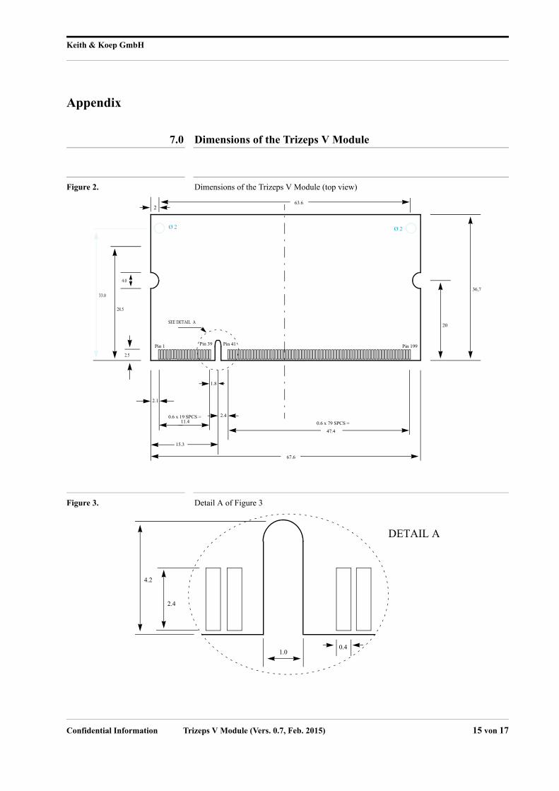
7.0 Dimensions of the Trizeps V Module
Figure 2. Dimensions of the Trizeps V Module (top view)
Figure 3. Detail A of Figure 3
Pin 1 Pin 39 Pin 41 Pin 199
67.6
2.1
11.4
1.8
2.4
47.4
0.6 x 19 SPCS =0.6 x 79 SPCS =
20
36,7
4.0
28.5
SEE DETAIL A
2.5
63.62
Ø 2 Ø 2
33.0
15.3
1.00.4
4.2
DETAIL A
2.4
Confidential Information Trizeps V Module (Vers. 0.7, Feb. 2015) 15 von 17
Keith & Koep GmbH
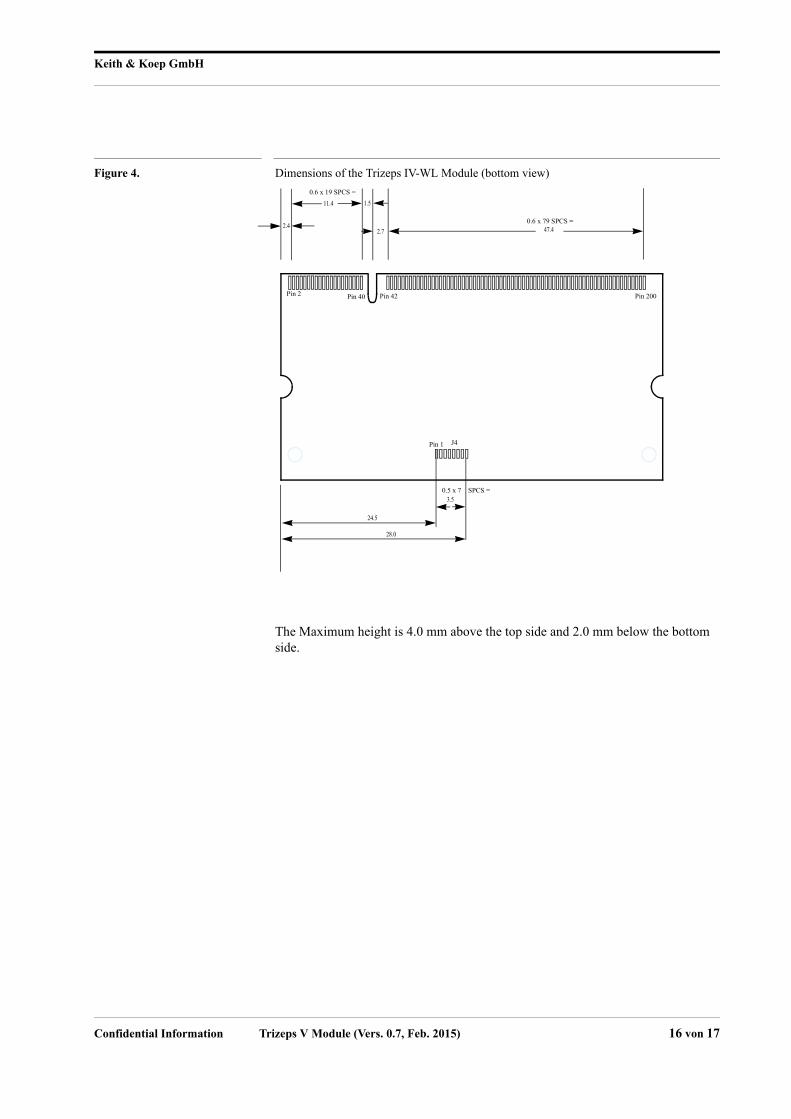
Figure 4. Dimensions of the Trizeps IV-WL Module (bottom view)
The Maximum height is 4.0 mm above the top side and 2.0 mm below the bottom side.
Pin 2 Pin 40 Pin 42 Pin 200
2.4
11.4
2.7
1.5
47.4
0.6 x 19 SPCS =
0.6 x 79 SPCS =
24.5
28.0
3.50.5 x 7 SPCS =
J4Pin 1
Confidential Information Trizeps V Module (Vers. 0.7, Feb. 2015) 16 von 17

Keith & Koep GmbH
Revision
Board: Trizeps V
Revision PCB number Date Changes
0.4 10.07.2008 Initial Version (preliminary)
0.5 10.11.2008 Added 256MB DDR option.
0.6 14.02.2013 Codec Change UCB1400 --> WM9715L
0.7 17.02.2015 Table 2 (description of Pin 164) rectified
Confidential Information Revision 17 von 17