transmitter optimization for ≥ 25gbps retimer links
TRANSCRIPT

1SNLA252–September 2017Submit Documentation Feedback
Copyright © 2017, Texas Instruments Incorporated
Transmitter Optimization for ≥ 25 Gbps Retimer Links
Application ReportSNLA252–September 2017
Transmitter Optimization for ≥ 25 Gbps Retimer Links
Rodrigo Natal
ABSTRACTThis report provides guidance on how to optimally configure the transmitter settings for 25/28G retimerapplications. Measurement examples are presented along with typical data for different test configurations.Moreover, the additional challenges involved for 25/28G data rate systems are discussed relative to theprevious generation systems.
Contents1 Retimer Applications ........................................................................................................ 32 Overview of TI 25G/28G Retimer Tx Output Signal Conditioning .................................................... 33 Configuring the Retimer Tx for ≥ 25Gbps System Challenges ........................................................ 5
List of Figures
1 Typical Uses of TI’s 8-Channel 25/28G Retimer in a Networking System ........................................... 32 Conceptual FIR Waveform with Negative Post-Cursor Only, with Positive Main-cursor ........................... 43 Conceptual FIR Waveform with Negative Pre-Cursor Only, with Positive Main-Cursor............................ 44 Conceptual FIR Waveform Illustrating Positive Post-Cursor On Rising Edge Transition With Positive
Main-Cursor .................................................................................................................. 55 SDD21 Plots for Measured SFP Compliance Test Channels; 1x2 Vertical SFP Cage Used ..................... 66 SFP+/SFP28 Module Compliance Test Setup Used for S-Parameter Evaluation .................................. 77 Measured Response for 10.3125 Gbps Data Rate Pulse, for an 8 dB Loss Channel.............................. 88 Measured Response for 25.78125 Gbps Data Rate Pulse, for an 8 dB Loss Channel ............................ 89 Setup Diagram For Nominal Retimer Test Case (e.g. Retimer Evaluation Board Level Testing) ............... 1010 Measured DS250DF810 25.78125 Gbps Output Eye Diagram with PRBS15, for Nominal Test Case and
Default FIR Settings (main = 26, pre-cursor = 0, post-cursor = 0) .................................................. 1011 Measured DS250DF810 25.78125 Gbps Output Eye Diagram with PRBS15, for Nominal Test Case and
Optimized FIR Settings (main = 22, pre-cursor = -2, post-cursor = 2) .............................................. 1112 Setup Diagram For Test Case of Retimer Evaluation Board Plus Mated QSFP28 Module Compliance
Board-Host Compliance Board Combination ........................................................................... 1213 DS250DF810 25.78125 Gbps Output for PRBS15 Pattern for Worst Case QSFP28 Host-to-module Test
Channel and No Tx Equalization Applied (main = 26, pre-cursor = 0, post-cursor = 0) .......................... 1314 DS250DF810 25.78125 Gbps Output for PRBS15 Pattern For Worst Case QSFP28 Host-to-module Test
Channel and Tx Equalization Applied (main = 16, pre-cursor = -3, post-cursor = -7) ............................ 1315 Block Diagram Illustrating the Component Edge Retimer Test Case ............................................... 1416 Measured DS250DF810 25.78125 Gbps Output Eye Diagram for PRBS15 pattern, for Nominal Test
Case And Default FIR Settings (main = 26, pre-cursor = 0, post-cursor = 0) ..................................... 1517 Measured DS250DF810 25.78125 Gbps Output Eye Diagram for PRBS15 Pattern After De-embedding
And With Optimized Fir Settings (main = 26, pre-cursor = -2, post-cursor = +1).................................. 1518 Backplane/Midplane Application Block Diagram ....................................................................... 1619 SDD21 Response for a ≥ 20 Gbps Backplane Reference Test System For Two Channel Cases ............. 1720 Retimer Test Setup Used For Evaluating Rx Eye Opening Performance As A Function of TX FIR Setting... 1821 DS250DF810 Eye Monitor Plot for 15-inch FR4 Test Card Case, for Default Tx FIR Settings ................. 1822 DS250DF810 Eye Monitor Plot for 15-inch FR4 Test Card Case, for Optimized Tx FIR Settings (main =
20 , post-cursor = 0, pre-cursor = -6 ) ................................................................................... 19

www.ti.com
2 SNLA252–September 2017Submit Documentation Feedback
Copyright © 2017, Texas Instruments Incorporated
Transmitter Optimization for ≥ 25 Gbps Retimer Links
23 Guideline for link Partner FIR Settings When Insertion Loss ≤ 15 dB .............................................. 2024 Guideline for Link Partner FIR Settings When Insertion Loss ≤ 25 dB ............................................. 2125 Guideline for Link Partner FIR Settings When Insertion Loss ≤ 35 dB.............................................. 22
List of Tables
1 DS250DF810 25.78125 Gbps Output Eye Measurements as a Function of FIR Pre-Cursor (post-cursor =0) ............................................................................................................................. 11
2 DS250DF810 25.78125 Gbps Output Eye Measurements as a Function of FIR Post-Cursor (pre-cursor =0) ............................................................................................................................. 11
3 DS250DF810 25.78125 Gbps Rx HEO and VEO Values as a Function of FIR Pre-cursor for 15-inch FR4Test Card Case (with post-cursor = 0) .................................................................................. 18
4 DS250DF810 25.78125 Gbps Rx HEO and VEO Values as a Function of FIR Post-cursor for 15-inchFR4 Test Card Case (with pre-cursor = 0).............................................................................. 19
5 DS250DF810 25.78125 Gbps Rx HEO and VEO Values as a Function of FIR Pre-cursor for 20-inch FR4Test Card Case (with post-cursor = 0) .................................................................................. 19
6 DS250DF810 25.78125 Gbps Rx HEO and VEO Values as a Function of FIR Post-cursor for 20-inchFR4 Test Card Case (with pre-cursor = 0).............................................................................. 19

www.ti.com Retimer Applications
3SNLA252–September 2017Submit Documentation Feedback
Copyright © 2017, Texas Instruments Incorporated
Transmitter Optimization for ≥ 25 Gbps Retimer Links
1 Retimer ApplicationsTI’s 25/28G family of retimers can be implemented in a variety of high-speed serial link applicationsrequiring reach extension and/or signal quality optimization. Figure 1 illustrates the types of interfaceswithin a networking system where retimers are typically implemented.
Figure 1. Typical Uses of TI’s 8-Channel 25/28G Retimer in a Networking System
2 Overview of TI 25G/28G Retimer Tx Output Signal ConditioningThe output driver for TI’s 25G/28G retimers has a three-tap finite impulse response (FIR) filter whichallows for pre- and post-cursor equalization to compensate for a wide variety of output channel media. Thefilter consists of a weighted sum of three consecutive retimed bits as shown in the following diagram. C[0]can take on values in the range [-31, +31]. C[-1] and C[+1] can take on values in the range [-15, 15].
When utilizing the FIR filter, it is important to abide by the following general rules:• |C[-1]|+|C[0]|+|C[+1]| ≤ 31; the FIR tap coefficients absolute sum must be less or equal to 31)• sgn(C[-1])=sgn(C[+1]) ≠ sgn(C[0]), for high-pass filter effect; the sign for the pre-cursor and/or post-
cursor tap must be different from main-cursor tap to realize boost effect• sgn(C[-1])=sgn(C[+1]) = sgn(C[0]), for low-pass filter effect; the sign for the pre-cursor and/or post-
cursor tap must be equal to the main-cursor tap to realize attenuation effect
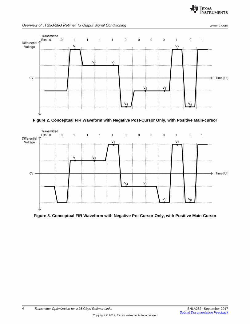
The FIR filter is used to pre-distort the transmitted waveform to compensate for frequency-dependent lossin the output channel. The most common way of pre-distorting the signal is to accentuate the transitionsand de-emphasize the non-transitions. The bit before a transition is accentuated via the pre-cursor tap,and the bit after the transition is accentuated via the post-cursor tap. Figure 2, Figure 3, Figure 4 belowgive a conceptual illustration of how the FIR filter affects the output waveform. The followingcharacteristics can be derived from the example waveforms:• VODpk-pk=v7 - v8• VODlow-frequency = v2 - v5• RpredB = 20 * log10 (v3 ⁄ v2 )• RpstdB = 20 * log10 (v1 ⁄ v2 )
Differential
Voltage
Time [UI]
v1 v2
v3
v4 v5
v6
v7
v8
0V
Transmitted
Bits: 0 0 1 1 1 1 0 0 0 0 1 0 1
Differential
Voltage
Time [UI]
v1
v2 v3
v4
v5 v6
v7
v8
0V
Transmitted
Bits: 0 0 1 1 1 1 0 0 0 0 1 0 1
Overview of TI 25G/28G Retimer Tx Output Signal Conditioning www.ti.com
4 SNLA252–September 2017Submit Documentation Feedback
Copyright © 2017, Texas Instruments Incorporated
Transmitter Optimization for ≥ 25 Gbps Retimer Links
Figure 2. Conceptual FIR Waveform with Negative Post-Cursor Only, with Positive Main-cursor
Figure 3. Conceptual FIR Waveform with Negative Pre-Cursor Only, with Positive Main-Cursor

Differential
Voltage
Time [UI]
v1
v2
0V
Transmitted
Bits: 0 0 1 1 1 1
www.ti.com Configuring the Retimer Tx for ≥ 25Gbps System Challenges
5SNLA252–September 2017Submit Documentation Feedback
Copyright © 2017, Texas Instruments Incorporated
Transmitter Optimization for ≥ 25 Gbps Retimer Links
Figure 4. Conceptual FIR Waveform Illustrating Positive Post-Cursor On Rising Edge Transition WithPositive Main-Cursor
3 Configuring the Retimer Tx for ≥ 25Gbps System Challenges
3.1 25/28G vs 10GSignal conditioning challenges are more significant for ≥ 25G applications compared to previous 10Gnetworking systems. Here are three challenges which are more prevalent in 25/28G applications:
1. Insertion loss
2. Reflections and crosstalk
3. Pre-cursor inter-symbol interference (ISI)
3.1.1 Insertion LossInsertion loss at the Nyquist frequency for a given electrical channel inherently increases with data rate.This becomes a signal conditioning issue when system designers want to reuse existing hardware (e.g. achassis with legacy backplane design), or when high-performance dielectric materials and connectors arecost prohibitive. As a simple example, Figure 5 shows the SDD21 parameter performance for a SFP host-to-module channel test case. Both SFP+ and SFP28 module compliance board channels are plotted. Theelectrical configuration used for the measurement is shown in Figure 6. As per the plots, the insertion lossat the 25.78125 Gbps Nyquist frequency of 12.89 GHz is significantly greater for the SFP+ plots than theSFP28 plots. This result is certainly not surprising, given the use of Nelco dielectric material and 5 GHzrated edge connector for the SFP+ compliance board versus the higher performance Megtron materialand 12 GHz edge connector used on the SFP28 compliance board.

Configuring the Retimer Tx for ≥ 25Gbps System Challenges www.ti.com
6 SNLA252–September 2017Submit Documentation Feedback
Copyright © 2017, Texas Instruments Incorporated
Transmitter Optimization for ≥ 25 Gbps Retimer Links
Blue trace: SFP+ cage topLight blue trace: SFP+ cage bottomGreen trace: SFP28 cage topRed trace: SFP28 cage bottom
Figure 5. SDD21 Plots for Measured SFP Compliance Test Channels; 1x2 Vertical SFP Cage Used

SFP Module Compliance Board
Cage/
Connector
Ele
ctrical
Loo
pp
ack
Mo
du
le
Network Analyzer
Port 1 Port 3
TD+ TD- RD+ RD-
Port 2 Port 4
www.ti.com Configuring the Retimer Tx for ≥ 25Gbps System Challenges
7SNLA252–September 2017Submit Documentation Feedback
Copyright © 2017, Texas Instruments Incorporated
Transmitter Optimization for ≥ 25 Gbps Retimer Links
Figure 6. SFP+/SFP28 Module Compliance Test Setup Used for S-Parameter Evaluation
3.1.2 Reflections and CrosstalkComponents and PCB traces behave less ideally at higher frequencies, due in large part to parasiticeffects. Parasitics (resistive, inductive, or capacitive) affect how the channel impedance behaves overfrequency. Moreover impedance mismatching results in signal reflection. Referring back to the exampleSDD12 plots in Figure 5 12 GHz all four plots start to show a significant amount of ripple. This is in starkcontrast to the fairly smooth characteristic for these plots below 10 GHz. This ripple on the transferfunction is usually indicative of reflection issues, and suggest that return loss must be examined. Thoughnot reviewed in this document, more pronounced parasitic effects and impedance mismatch at higher datarates can also lead to higher crosstalk between adjacent data channels.
Configuring the Retimer Tx for ≥ 25Gbps System Challenges www.ti.com
8 SNLA252–September 2017Submit Documentation Feedback
Copyright © 2017, Texas Instruments Incorporated
Transmitter Optimization for ≥ 25 Gbps Retimer Links
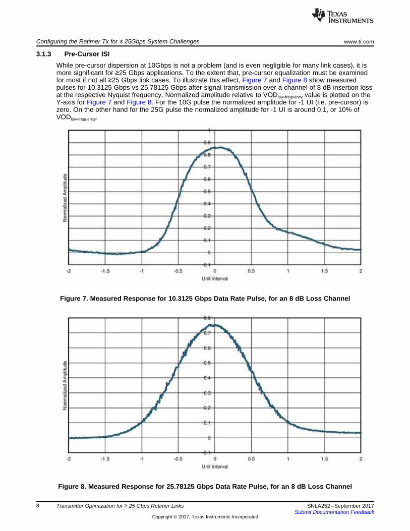
3.1.3 Pre-Cursor ISIWhile pre-cursor dispersion at 10Gbps is not a problem (and is even negligible for many link cases), it ismore significant for ≥25 Gbps applications. To the extent that, pre-cursor equalization must be examinedfor most if not all ≥25 Gbps link cases. To illustrate this effect, Figure 7 and Figure 8 show measuredpulses for 10.3125 Gbps vs 25.78125 Gbps after signal transmission over a channel of 8 dB insertion lossat the respective Nyquist frequency. Normalized amplitude relative to VODlow-frequency value is plotted on theY-axis for Figure 7 and Figure 8. For the 10G pulse the normalized amplitude for -1 UI (i.e. pre-cursor) iszero. On the other hand for the 25G pulse the normalized amplitude for -1 UI is around 0.1, or 10% ofVODlow-frequency.
Figure 7. Measured Response for 10.3125 Gbps Data Rate Pulse, for an 8 dB Loss Channel
Figure 8. Measured Response for 25.78125 Gbps Data Rate Pulse, for an 8 dB Loss Channel

www.ti.com Configuring the Retimer Tx for ≥ 25Gbps System Challenges
9SNLA252–September 2017Submit Documentation Feedback
Copyright © 2017, Texas Instruments Incorporated
Transmitter Optimization for ≥ 25 Gbps Retimer Links
3.2 3.2 Port-Side OptimizationThe typical port-side application requires a switch ASIC to interface to physical media enablingtransmission over some length of cable, be it optical fiber or copper cable of some type. Listed below arethree port-side interface functions where the retimer plays an important role:• Compensation of insertion loss for the host channel between the ASIC Tx and the port – The retimer is
relied on to improve the horizontal and vertical eye opening observed at the port-side module electricalinput by compensating for the host channel insertion loss via its equalization functions
• Compliance to module electrical input criteria for error free data transmission with margin – beyondinsertion loss compensation, module interfaces have electrical requirements which are commonlyspecified on network interface standards such as IEEE802.3 or Multi-Source Agreement (MSA)specifications such as Small Form Factor (SFF). These requirements may include strict limits for eyeheight and jitter. Physical medium dependent interfaces are sensitive to non-compensable jitter at themodule electrical input which may propagate through the link and result in degraded bit error ratesand/or link distance. The retimer’s clock and data recovery function produces a version of the inputdata with much less jitter, thus improving link performance margin.
• ASIC Rx input electrical eye opening optimization – the impairments present through the host channelmay lead to observing bit errors at the ASIC Rx if not sufficiently compensated for. Depending on theimpairments, which include a combination of insertion loss, noise and reflections, the ASIC Rx may nothave enough equalization capability and thus a signal conditioning device such as a retimer is requiredin the link.
To illustrate how to optimally configure the retimer Tx, three different evaluation cases applicable to port-side are examined:• Nominal case (e.g. retimer evaluation board level testing)• Component edge test point case• Module compliance channel test case
Figure 9 shows the nominal evaluation case where a TI DS250DF810 25 Gbps 8-channel retimer isimplemented on a board with SMA connector inputs and outputs. The total insertion loss for the boardtrace, connectors and cables for this setup type is typically around 6 dB for one direction (e.g. from retimerdevice output to scope input), which is within the typical specification range for a standard host-to-modulechannel. Hence, this retimer test setup is a useful transmitter evaluation case for port-side application,ahead of evaluation with module specific test fixtures.
Figure 10 shows a measured retimer output eye diagram for the default FIR settings. The measured eyeopening can be improved by applying some Tx equalization via the FIR taps. Figure 11 shows theoptimized eye diagram. As can be seen, the eye height was improved from 331 mV to 457 mV. Table 1and Table 2 further illustrate how the eye opening is affected by the FIR pre-cursor and post-cursorsetting. For the FIR pre-cursor tap with negative polarity, the vertical eye opening will improve as afunction of magnitude until compensable inter-symbol interference from dispersion is removed. Beyondthis point further increases in the FIR pre-cursor magnitude will translate to smaller vertical eye openingimprovements but an increase in peak-to-peak jitter. Data dependent jitter increases as a result of signalover-equalization for this condition. Similarly, for the FIR post-cursor tap with negative polarity, the verticaleye opening will improve as a function of magnitude until channel insertion loss is compensated for.Beyond this point further increases in the FIR post-cursor magnitude will translate to smaller vertical eyeopening improvement but an increase in peak-to-peak jitter.

Signal
Generator
DS250DF810 Evaluation
Board
RX0P TX0P Sampling
ScopeTx0NRX0N
SMA
cables
SMA
cables
Configuring the Retimer Tx for ≥ 25Gbps System Challenges www.ti.com
10 SNLA252–September 2017Submit Documentation Feedback
Copyright © 2017, Texas Instruments Incorporated
Transmitter Optimization for ≥ 25 Gbps Retimer Links
Figure 9. Setup Diagram For Nominal Retimer Test Case (e.g. Retimer Evaluation Board Level Testing)
Figure 10. Measured DS250DF810 25.78125 Gbps Output Eye Diagram with PRBS15, for Nominal TestCase and Default FIR Settings (main = 26, pre-cursor = 0, post-cursor = 0)

www.ti.com Configuring the Retimer Tx for ≥ 25Gbps System Challenges
11SNLA252–September 2017Submit Documentation Feedback
Copyright © 2017, Texas Instruments Incorporated
Transmitter Optimization for ≥ 25 Gbps Retimer Links
Figure 11. Measured DS250DF810 25.78125 Gbps Output Eye Diagram with PRBS15, for Nominal TestCase and Optimized FIR Settings (main = 22, pre-cursor = -2, post-cursor = 2)
Table 1. DS250DF810 25.78125 Gbps Output Eye Measurements as a Function of FIR Pre-Cursor(post-cursor = 0)
PRE-CURSOR VALUE EYE HEIGHT (mV) JITTER p-p (ps)0 328 6.5-1 365 5.4-2 390 6.3-3 415 7.1-4 435 7.2-5 443 8.1
Table 2. DS250DF810 25.78125 Gbps Output Eye Measurements as a Function of FIR Post-Cursor(pre-cursor = 0)
POST-CURSOR VALUE EYE HEIGHT (mV) JITTER p-p (ps)0 328 6.5-1 359 6.3-2 384 7-3 406 7.4-4 417 8.6-5 414 8.9
Figure 12 shows a test setup that adds a QSFP28 mated module compliance board-host complianceboard pair to the channel from Figure 9. This test case has worse insertion loss than the typical modulehost channel in a networking system, as two separate fixtures are being used combined with externalSMA cables. The total insertion loss for this system is around 12 dB at 12.89 GHz. Figure 13 shows themeasured output eye diagram when no Tx equalization is applied. Vertical eye opening is rather impairedwith a value in the tens of millivolts range. TI’s 25/28G retimers however have ample Tx equalization, andare thus more than capable of opening up the eye for this implementation case. Figure 14 shows theresulting eye diagram after applying Tx equalization via the FIR taps. As can be seen from the Figure 12the resulting eye height of 204mV allows compliance to the CAUI-4 chip-to-module eye mask.

QSFP28 Module Compliance Board
Cage/
Connector
Ho
st
Co
mp
lian
ce
Bo
ard
DS250DF810 Retimer Evaluation Board
TX0P TX0N
Keysight DCAx with
86108B Precision
Timebase Module
RX0P RX0N
Signal Generator
Configuring the Retimer Tx for ≥ 25Gbps System Challenges www.ti.com
12 SNLA252–September 2017Submit Documentation Feedback
Copyright © 2017, Texas Instruments Incorporated
Transmitter Optimization for ≥ 25 Gbps Retimer Links
Figure 12. Setup Diagram For Test Case of Retimer Evaluation Board Plus Mated QSFP28 ModuleCompliance Board-Host Compliance Board Combination

www.ti.com Configuring the Retimer Tx for ≥ 25Gbps System Challenges
13SNLA252–September 2017Submit Documentation Feedback
Copyright © 2017, Texas Instruments Incorporated
Transmitter Optimization for ≥ 25 Gbps Retimer Links
Figure 13. DS250DF810 25.78125 Gbps Output for PRBS15 Pattern for Worst Case QSFP28 Host-to-module Test Channel and No Tx Equalization Applied (main = 26, pre-cursor = 0, post-cursor = 0)
Figure 14. DS250DF810 25.78125 Gbps Output for PRBS15 Pattern For Worst Case QSFP28 Host-to-module Test Channel and Tx Equalization Applied (main = 16, pre-cursor = -3, post-cursor = -7)

Retimer TXTest Channel
Retimer RX
Component Edge Component Edge
Configuring the Retimer Tx for ≥ 25Gbps System Challenges www.ti.com
14 SNLA252–September 2017Submit Documentation Feedback
Copyright © 2017, Texas Instruments Incorporated
Transmitter Optimization for ≥ 25 Gbps Retimer Links
Figure 15 illustrates the test case where the test points are defined right at the input or output of theretimer device. Specifications such as IEEE802.3 and SFF MSA may define such test points as part oftheir definitions of chip-to-module interfaces. The “component edge” may be specified at the retimerpackage interface point (e.g. BGA ball) or perhaps a small PCB trace distance from this point.
For transmitter output measurements at the component edge a useful methodology is to take advantageof the de-emdedding function that is implemented in newer oscilloscopes such as the Keysight DCA-X. Ifthe s-parameters for the test channel have been obtained, the scope de-embed function then allows theuser to remove this s-parameter contribution from the measured waveform. Figure 16 super-imposes theoutput eye diagram measured with the setup of Figure 9 with the waveform resulting from removing theS4P for the evaluation board channel. Figure 17 shows the resulting output eye diagram after optimizingthe FIR settings. The post-cursor of +1 represents a small amount of attenuation that is being applied tothe signal to eliminate residual peaking on the output waveform. The FIR pre-cursor setting of -2compensates for the small amount of pre-cursor dispersion in the channel.
Figure 15. Block Diagram Illustrating the Component Edge Retimer Test Case

www.ti.com Configuring the Retimer Tx for ≥ 25Gbps System Challenges
15SNLA252–September 2017Submit Documentation Feedback
Copyright © 2017, Texas Instruments Incorporated
Transmitter Optimization for ≥ 25 Gbps Retimer Links
Blue trace: non-dembedded waveformPurple trace: waveform after removing S4P for the evaluation board channel
Figure 16. Measured DS250DF810 25.78125 Gbps Output Eye Diagram for PRBS15 pattern, for NominalTest Case And Default FIR Settings (main = 26, pre-cursor = 0, post-cursor = 0)
Figure 17. Measured DS250DF810 25.78125 Gbps Output Eye Diagram for PRBS15 Pattern After De-embedding And With Optimized Fir Settings (main = 26, pre-cursor = -2, post-cursor = +1)

Line CardSwitch Fabric Card
DS
25
0D
F8
10
DS
25
0D
F8
10
ASIC
FPGA
x8 25G
x8 25G
ASIC
FPGA
Co
nn
ecto
r
Co
nn
ecto
r
Passive Backplane/
Midplane
Configuring the Retimer Tx for ≥ 25Gbps System Challenges www.ti.com
16 SNLA252–September 2017Submit Documentation Feedback
Copyright © 2017, Texas Instruments Incorporated
Transmitter Optimization for ≥ 25 Gbps Retimer Links
3.3 3.3 Midplane/Backplane OptimizationFigure 18 below illustrates the typical backplane/midplane configuration in a networking system. High-speed data transmission over the typical backplane involves signal launch through a passive channel withtwo or more multi-pin electrical connectors, and over long lengths of PCB trace. Given the expected signalimpairments, 25/28G backplane applications have rather challenging system requirements. TheIEEE802.3 100GBASE-KR4 specification is one example reference point for ≥ 25 Gbps backplaneapplication requirements. This clause specifies requirements for a 4x25.78125Gbps backplane interfaceand includes requirements for both transmit and receive test points:• The transmit path requirements include specifications for output voltages, return loss, and jitter as well
as output waveform characteristics including support of pre-cursor and post-cursor equalization• The receive path requirements include interference tolerance and jitter tolerance requirements, plus a
specified channel insertion loss of 30 dB to 35 dB at the Nyquist frequency
Figure 18. Backplane/Midplane Application Block Diagram
As illustrated in Figure 18, the optimum placement for the retimer in a backplane/mid-plane application iswith the higher-loss channel segment at the input and the lower-loss channel segment at the output. Thisreduces the equalization burden on the downstream ASIC/FPGA, as the DS250DF810 is equalizing amajority of the overall channel. This type of asymmetric placement is not a requirement, but when anasymmetric placement is required due to the presence of a passive backplane or mid-plane, then thisbecomes the recommended placement. Figure 19 shows the measured SDD21 response for a referencetest system representative of a 25/28G backplane. Consistent with the typical requirements listed above,the insertion loss ranges from 27 dB to 35 dB at 12.89 GHz.

www.ti.com Configuring the Retimer Tx for ≥ 25Gbps System Challenges
17SNLA252–September 2017Submit Documentation Feedback
Copyright © 2017, Texas Instruments Incorporated
Transmitter Optimization for ≥ 25 Gbps Retimer Links
Blue trace: 27.84 dB loss at 12.89 GHzGreen trace: 35.45 dB loss at 12.89 GHz
Figure 19. SDD21 Response for a ≥ 20 Gbps Backplane Reference Test System For Two Channel Cases
For backplane/midplane interconnects within a system a common question that arises is what level of Txpre-cursor and post-cursor equalization to apply to achieve best link performance. One way to assess linkperformance is to evaluate the horizontal eye opening (HEO) and vertical eye opening (VEO) that can berealized at the Rx input after equalization. TI’s 25/28G retimers implement a Eye Opening Monitor (EOM)which for its default setting records HEO and VEO values corresponding to bit error rate in the order of1E-7. TI’s 25/28G retimers such as the DS250DF810 25Gbps 8-channel retimer have strong Rxequalization capability that allow it to recover data over channels of up to 35 dB of insertion loss.Specifically, the TI retimer has both an adaptive Continuous Time Linear Equalizer (CTLE) and adaptiveDecision Feedback Equalizer (DFE) in its Rx chain. Given all of the post-cursor equalization power of theretimer Rx coupled with its adaptive configuration, it is more efficient and optimal for the link to rely on theRx to handle as much of the post-cursor equalization as possible. Additionally, the DFE in particular isable to compensate for reflection and crosstalk effects, while the Tx equalization offers a marginal at bestassistance for these two types of signal impairment.
The setup shown in Figure 20 was used to help quantify how Rx HEO and VEO will vary with Tx pre-cursor and post-cursor in a high insertion loss system. Both 15-inch and 20-inch FR4 PCB test cardswhere used as part of the test system for the measurements. The total channel insertion loss for eachcase respectively is around 35 dB and 44 dB. The TI retimer Rx was set to its adapt mode 2 for the tests(both CTLE and DFE enabled).
Based on the observed results it is most useful for link performance to use the Tx to apply pre-cursorequalization. This result is not too surprising as the CTLE and DFE Rx equalization blocks in the TIretimer are not able to compensate for the pre-cursor dispersion. On the other hand, applying Tx post-cursor is not that useful to further improve link performance for the cases when the overall insertion loss iswithin the compensation capability of the Rx. Figure 23, Figure 24 and Figure 25 below give generalrecommendations for pre- and post-cursor for different channel loss conditions. The insertion loss (IL) inthese plots refers to the total loss between the link partner transmitter and the DS250DF810 receiver. It isimportant to emphasize that the ideal metric for link performance is bit error rate at the Rx input.HEO/VEO at the Rx input is the next best alternative, as HEO and VEO are correlated to a bit error ratevalue. Optimization of Tx equalization settings based on performance measured at intermediate test pointswithin a backplane channel is not recommended.

Signal
Generator
DS250DF810 Evaluation
Board
RX0P TX0P
FR4 Test
Card
Tx0NRX0N
RX1P
RX1N
Configuring the Retimer Tx for ≥ 25Gbps System Challenges www.ti.com
18 SNLA252–September 2017Submit Documentation Feedback
Copyright © 2017, Texas Instruments Incorporated
Transmitter Optimization for ≥ 25 Gbps Retimer Links
Figure 20. Retimer Test Setup Used For Evaluating Rx Eye Opening Performance As A Function of TXFIR Setting
Table 3. DS250DF810 25.78125 Gbps Rx HEO and VEO Values as a Function of FIR Pre-cursor for15-inch FR4 Test Card Case (with post-cursor = 0)
Pre-cursor value HEO (UI) VEO (mV)0 0.65 240-1 0.68 252-2 0.68 264-3 0.68 270-4 0.68 276-5 0.66 273-6 0.65 282-7 0.62 282-8 0.56 282
Figure 21. DS250DF810 Eye Monitor Plot for 15-inch FR4 Test Card Case, for Default Tx FIR Settings

www.ti.com Configuring the Retimer Tx for ≥ 25Gbps System Challenges
19SNLA252–September 2017Submit Documentation Feedback
Copyright © 2017, Texas Instruments Incorporated
Transmitter Optimization for ≥ 25 Gbps Retimer Links
Figure 22. DS250DF810 Eye Monitor Plot for 15-inch FR4 Test Card Case, for Optimized Tx FIR Settings(main = 20 , post-cursor = 0, pre-cursor = -6 )
Table 4. DS250DF810 25.78125 Gbps Rx HEO and VEO Values as a Function of FIR Post-cursor for15-inch FR4 Test Card Case (with pre-cursor = 0)
POST-CURSOR VALUE HEO (UI) VEO (mV)-1 0.62 246-2 0.56 240-3 0.53 222-4 0.5 228-5 0.4 204-6 0.34 168
Table 5. DS250DF810 25.78125 Gbps Rx HEO and VEO Values as a Function of FIR Pre-cursor for20-inch FR4 Test Card Case (with post-cursor = 0)
PRE-CURSOR VALUE HEO (UI) VEO (mV)0 0.4375 143.75-1 0.4375 162.5-2 0.4375 187.5-3 0.5 200-4 0.5 200-5 0.5 212.5-6 0.5 212.5-7 0.5 212.5-8 0.4375 212.5
Table 6. DS250DF810 25.78125 Gbps Rx HEO and VEO Values as a Function of FIR Post-cursor for20-inch FR4 Test Card Case (with pre-cursor = 0)
POST-CURSOR VALUE HEO (UI) VEO (mV)-1 0.375 150-2 0.375 137.5-3 0.3125 125

Configuring the Retimer Tx for ≥ 25Gbps System Challenges www.ti.com
20 SNLA252–September 2017Submit Documentation Feedback
Copyright © 2017, Texas Instruments Incorporated
Transmitter Optimization for ≥ 25 Gbps Retimer Links
Table 6. DS250DF810 25.78125 Gbps Rx HEO and VEO Values as a Function of FIR Post-cursor for20-inch FR4 Test Card Case (with pre-cursor = 0) (continued)
POST-CURSOR VALUE HEO (UI) VEO (mV)-4 0.25 125-5 0.125 62.5-6 0.125 62.5
Figure 23. Guideline for link Partner FIR Settings When Insertion Loss ≤ 15 dB

www.ti.com Configuring the Retimer Tx for ≥ 25Gbps System Challenges
21SNLA252–September 2017Submit Documentation Feedback
Copyright © 2017, Texas Instruments Incorporated
Transmitter Optimization for ≥ 25 Gbps Retimer Links
Figure 24. Guideline for Link Partner FIR Settings When Insertion Loss ≤ 25 dB

Configuring the Retimer Tx for ≥ 25Gbps System Challenges www.ti.com
22 SNLA252–September 2017Submit Documentation Feedback
Copyright © 2017, Texas Instruments Incorporated
Transmitter Optimization for ≥ 25 Gbps Retimer Links
Figure 25. Guideline for Link Partner FIR Settings When Insertion Loss ≤ 35 dB

IMPORTANT NOTICE AND DISCLAIMER
TI PROVIDES TECHNICAL AND RELIABILITY DATA (INCLUDING DATASHEETS), DESIGN RESOURCES (INCLUDING REFERENCE DESIGNS), APPLICATION OR OTHER DESIGN ADVICE, WEB TOOLS, SAFETY INFORMATION, AND OTHER RESOURCES “AS IS” AND WITH ALL FAULTS, AND DISCLAIMS ALL WARRANTIES, EXPRESS AND IMPLIED, INCLUDING WITHOUT LIMITATION ANY IMPLIED WARRANTIES OF MERCHANTABILITY, FITNESS FOR A PARTICULAR PURPOSE OR NON-INFRINGEMENT OF THIRD PARTY INTELLECTUAL PROPERTY RIGHTS.These resources are intended for skilled developers designing with TI products. You are solely responsible for (1) selecting the appropriate TI products for your application, (2) designing, validating and testing your application, and (3) ensuring your application meets applicable standards, and any other safety, security, or other requirements. These resources are subject to change without notice. TI grants you permission to use these resources only for development of an application that uses the TI products described in the resource. Other reproduction and display of these resources is prohibited. No license is granted to any other TI intellectual property right or to any third party intellectual property right. TI disclaims responsibility for, and you will fully indemnify TI and its representatives against, any claims, damages, costs, losses, and liabilities arising out of your use of these resources.TI’s products are provided subject to TI’s Terms of Sale (www.ti.com/legal/termsofsale.html) or other applicable terms available either on ti.com or provided in conjunction with such TI products. TI’s provision of these resources does not expand or otherwise alter TI’s applicable warranties or warranty disclaimers for TI products.
Mailing Address: Texas Instruments, Post Office Box 655303, Dallas, Texas 75265Copyright © 2020, Texas Instruments Incorporated