transmission lines - byuece360web.groups.et.byu.net/notes/old_notes_vectors1.pdf · transmission...
TRANSCRIPT

Chapter 1
Transmission Lines
A transmission line guides energy from one point to another in such a way that the energy doesnot spread as it propagates. Transmission line examples include
• Coaxial cables (network, television)
• Twisted pair lines (telephone, network)
• Waveguides, optical fibers
• Printed circuit board trace; metalized line on an integrated circuit
• Power lines
• Earth/ionosphere system
The circuit diagram symbol for a transmission line is two wires with junctions marked as smallcircles:
Figure 1.1: Circuit diagram symbol for a transmission line.
Circuit theory is an approximation to Maxwell’s equations of electromagnetism. In a circuit, whenthe voltage between two nodes on a pair of wires is changed at one location, the voltage between
1

any other pair of nodes on the same wires changes instantaneously. But in reality, the voltagechange cannot propagate faster than the speed of light.
Transmission line theory can be viewed as a correction to circuit theory that is needed when wiresor other conductors in a system are long enough that this propagation delay along the wires orconductors cannot be neglected.
One important aspect of transmission line theory is that many different types of lines, includingsystems that do not appear to be transmission lines at all, such as optical coatings and evenempty space, can be treated using the same basic set of equations. We will study the behaviorof transmission lines for two types of driving sources: transients or pulses, and sinusoidal or timeharmonic excitation.
1.1 Transmission Line Equations
How can we analyze the behavior of currents and voltages on a transmission line? We need aset of equations that govern the currents and voltages at different locations along the line. Oneway to arrive at these equations is to model the transmission line as a sequence of lumped circuitelements. The inductance and capacitance provide the propagation delay as energy moves alongthe transmission line, and the resistance represents losses. One can then take the limit as the lengthof the lumped-element section goes to zero, and arrive at a set of partial differential equations forthe current and voltage on the transmission line.
Figure 1.2: Lumped element model for a short section of a transmission line.
In the lumped element model, it is convenient to represent the capacitance, inductance, and resis-tance as per-unit-length quantities, so that
L = Inductance per unit length (H/m) (1.1)C = Capacitance per unit length (F/m) (1.2)R = Resistance per unit length (Ω/m) (1.3)G = Conductance per unit length (S/m) (1.4)
It is helpful at this point to understand these quantities in terms of a particular transmission lineexample. For a simple pair of parallel wires, L∆z represents energy stored in the magnetic fieldaround the wires for a section of length ∆z. C∆z represents the capacitance between the two pieces
2

of wire. R∆z represents the series resistance of the wires, and G∆z represents parallel conductanceof the dielectric material around the wires.
Lossless line. If the dielectric material between the conductors is a perfect insulator, then G = 0.If the conductors making up the transmission line are perfect, then R = 0. In this case, the lineis said to be lossless. Real transmission lines are lossy, but in many cases the loss is small, so it isvery common to approximate a transmission line as lossless.
1.1.1 Telegrapher Equations
Applying Kirchoff’s voltage law (KVL) around the loop leads to
v(z, t)− i(z, t)R∆z − L∆z∂i(z, t)
∂t− v(z + ∆z, t) = 0 (1.5)
v(z, t)− v(z + ∆z, t) = ∆z
[i(z, t)R + L
∂i(z, t)∂t
](1.6)
−[v(z + ∆z, t)− v(z, t)
∆z
]= Ri(z, t) + L
∂i(z, t)∂t
(1.7)
When we let ∆z → 0, the left hand side becomes the definition of a derivative, so that
−∂v(z, t)∂z
= Ri(z, t) + L∂i(z, t)
∂t(1.8)
Using Kirchoff’s current law at the top left node, we obtain
i(z, t)−G∆Zv(z + ∆z, t)− C∆z∂v(z + ∆z, t)
∂t− i(z + ∆z, t) = 0 (1.9)
Again taking the limit as ∆z → 0, this equation becomes
−∂i(z, t)∂z
= Gv(z, t) + C∂v(z, t)
∂t(1.10)
Equations (1.8) and (1.10) are known as the Telegrapher equations.
1.1.2 Wave Equation
The Telegrapher equations are coupled first order partial differential equations. Since it is simplerto solve a single second order differential equation, we combine these two equations into a singleequation. We first take the derivative of Eq. (1.8) with respect to z, to obtain
−∂2v
∂z2= R
∂i
∂z+ L
∂2i
∂t∂z(1.11)
3

We can substitute ∂ti from Eq. (1.10). We also need ∂tzi, which we can get by differentiating Eq.(1.10) with respect to t:
− ∂2i
∂z∂t= G
∂v
∂t+ C
∂2v
∂t2(1.12)
Substituting Eqs. (1.10) and (1.12) into Eq. (1.11) leads to
−∂2v
∂z2= −R
− ∂i∂z︷ ︸︸ ︷[
Gv + C∂v
∂t
]−L
− ∂2i∂t ∂z︷ ︸︸ ︷[
G∂v
∂t+ C
∂2v
∂t2
](1.13)
∂2v
∂z2= RGv + (RC + LG)
∂v
∂t+ LC
∂2v
∂t2(1.14)
This is a second order partial differential equation, where the only unknown is the voltage v(z, t)on the transmission line. This is called the wave equation. A similar equation for i(z, t) could bederived by eliminating the voltage instead, but once we know the voltage on the line, the currentcan be found using the transmission line equations.
1.1.3 Wave Solutions
How do we solve the wave equation (1.14)? Most of the time when we use differential equations inengineering, we look up or remember the general form of the solution and solve for the unknownsusing initial or boundary conditions. For the wave equation, in the lossless case the general solutionconsists of two traveling waves of the form
v(z, t) = v+(z − ut) + v−(z + ut) (Lossless line) (1.15)
The term v+(z − ut) represents a pulse or wave traveling to the right (+z direction), and v−
represents a pulse traveling to the left (−z direction). The functions v+ and v− depend on theexcitation of the transmission line, and the constant u is determined by the coefficients of the waveequation.
Let’s look at the first part of the general solution where the excitation produces a square pulse asgiven by
p(x) =
1 |x| < 10 otherwise
(1.16)
We will set v+(z − ut) = p(z − ut). At time t = 0, the pulse v+(z) is centered at z = 0. At thetime t = to the pulse becomes
v+(z − uto) =
1 |z − uto| < 10 otherwise
(1.17)
The pulse is now centered at the position z = uto. The pulse has moved in the +z direction. Theresulting velocity is given by
velocity =∆z
∆t=
utoto
= u (1.18)
The other part of the general solution v−(z + ut) travels at the same velocity in the −z direction.
4

1.1.4 Phase Velocity
To solve for the constant u, we plug either part of the general solution (1.15) into the wave equation.Using the chain rule for the derivative,
∂2
∂z2v+(z − ut) = v+′′(z − ut) (1.19)
where the primes denote ordinary differentiation. Follow the same process to get the second deriva-tive with respect to time leads to
∂2
∂t2v+(z − ut) = v+′′(z − ut)(−u)2 (1.20)
Substituting these two terms into the wave equation gives
v+′′(z − ut) = LC u2 v+′′(z − ut). (1.21)
In order for this equality to hold, we must have that u2LC = 1, so that
u =1√LC
(Phase velocity) (1.22)
This quantity is called the phase velocity of waves on the transmission line.
For some common transmission lines, the phase velocity is
Coaxial Cable :1√LC
=
(√2π
µ ln(b/a)
)(√ln(b/a)
2πε
)=
1√µε
(1.23)
Two Wire :1√LC
=1√µε
(1.24)
Parallel Plate :1√LC
=1√µε
(1.25)
where µ and ε are parameters of the material separating the conductors. For these transmissionlines, the velocity only depends on the properties of the material around the transmission line,not the geometry. For transmission lines which consist of a dielectric (insulator) and a pair ofconductors, µ = µo, where µo is the permeability of free space (µo = 4π× 10−7 H/m), and ε = εrεo,where εo is the permittivity of free space (εo ' 8.854×10⁻¹² F/m) and εr is the relative permittivityof the dielectric. A typical value for the phase velocity is
u =1√µε
= (1√
µo εo)(
1√εr
) =c√εr≈ 2
3c (1.26)
where c ' 3× 10⁸ m/s is the speed of light in a vacuum.
5

1.1.5 Characteristic Impedance
For a lossless line, the first of the two telegrapher’s equations is
−∂v
∂zv = L
∂i
∂t(1.27)
Let us consider just the forward traveling wave,
− ∂
∂zv+(z − ut) = L
∂
∂ti+(z − ut) (1.28)
Using the chain rule this becomes
−v+′(z − ut) = L (−u)i+′(z − ut) (1.29)
Integrating both side with respect to x = z − ut gives
−∫
v+′(x) dx = −u L
∫i+′(x) dx (1.30)
−v+ = −uLi+ + constant (1.31)
Since i+ = 0 if v+ = 0, the constant is zero, and we have
v+
i+= u L =
L√L C
=
√L
C(1.32)
The constant on the right-hand side has units of Ohms, and we call this the ”characteristicimpedance” of the line:
Zo =
√L
C(1.33)
If we repeat this derivation for the reverse traveling wave, we get
v−
i−= −u L = −
√L
C= −Zo (1.34)
The total current can then be related to the total voltage using
v(z, t) = v+(z − ut) + v−(z + ut) (1.35)
i(z, t) =v+(z − ut)
Zo− v−(z + ut)
Zo(1.36)
This allows us to find the current on a transmission line if we know the forward and reverse voltagewaveforms.
The minus sign in the second equation is important. The characteristic impedance Zo is not a simpleresistance produced by the conductors in the line, because even a transmission line constructed fromperfect conductors has a finite, nonzero characteristic impedance. An impedance is the ratio of totalvoltage to total current, whereas the characteristic impedance is the ratio of the forward voltagewaveform to the associated current and the negative of the ratio of the reverse voltage waveform tothe associated current. If Eq. (1.36) had a positive sign instead of a negative sign, then Zo wouldbe a regular impedance. Can you understand this minus sign physically?
6

1.2 Transients on Transmission Lines
Consider the transmission line circuit in Fig. 1.3. When the switch closes a step voltage appears
Figure 1.3: Transmission line circuit.
across the generator end of the line. What is the value of that voltage? The characteristic impedanceis not the total impedance of the line but rather the relationship between the forward and reversetraveling voltages and currents. But when the switch first closes there is no reverse wave, becausethe forward step has not had time to travel down to the end and back. Therefore, the characteristicimpedance of the line is the total impedance of the line imediately after the switch closes. Thisleads to the equivalent circuit shown in Fig. 1.4 when the switch is first closed. From the equivalent
Figure 1.4: Equivalent circuit at t = 0.
circuit we can use a voltage divider relationship to calculate the magnitude of the step voltage,
v+1 (z = 0, t = 0) =
Zo
Zo + RgVg (1.37)
This initial pulse then starts to travel down the line at speed u. At time t = `/(2u), for examplethe step is halfway down the line. At t = `/u, the step arrives at the load.
1.2.1 Reflection Coefficient
What happens when the step hits the load? The pulse will reflect, and the v− term in the waveequation solution will no longer be zero. We need to find the amplitude of the reflected wave. Thisis easy to do using boundary conditions at the load end of the transmission line. The boundary
7

conditions are
v(`, T ) = vL(T ) (1.38)i(`, T ) = iL(T ) (1.39)
where T = `/u and vL(T ) and iL(T ) are the voltage across and the current through the loadresistor. vL and iL are related by Ohm’s law: vL = iLRL. Putting Ohm’s law together with theboundary conditions at the load end of the line, we obtain
v(`, T ) = RLi(`, T ) (1.40)
Using Eqs. (1.35) and (1.36), this can be rewritten as
v+1 + v−1 = RL
[v+1
Zo− v−1
Zo
](1.41)
where the line voltages and currents are all evaluated at z = ` and t = T . Solving this for v−1 gives
v−1 =RL − Zo
RL + Zov+1 (1.42)
We call the constant in this expression the load reflection coefficient:
ΓL =RL − Zo
RL + Zo(Load reflection coefficient) (1.43)
From this we can find the magnitude of the reflected wave:
v−1 = ΓLv+1 =
RL − Zo
RL + Zo
Zo
Zo + RgVg (1.44)
The voltage waveform on the transmission line at a time that is after the reflection from the load,and before the reflected pulse arrives at the generator, is shown in Fig. 1.5.
Figure 1.5: Voltage waveform at time t = 3T/2.
What happens when the reflected wave gets back to the generator? Using the same idea as at theload end, we can show that
v+2 =
Rg − Zo
Rg + Zov−1 = Γgv
−1 = ΓgΓLv+
1 (1.45)
Can you derive this expression on your own?
8

Figure 1.6 shows the voltage waveform after the reflected pulse has reflected again from the gener-ator end of the transmission line. The total voltage at a point on the transmission line is the sumof all the reflected and forward steps (v+
1 , v−1 , v+2 ) that have occured up until the current time.
Figure 1.6: Voltage waveform at time t = 9T/4.
If we look at the results we have found so far, we can see a pattern:
v+1 = Zo
Zo+RgVg (Voltage divider at t = 0)
v−1 = ΓLv+1 (First reflection at the load)
v+2 = ΓgΓLv+
1 (Reflection at generator)v−2 = ΓLΓgΓLv+
1
v+3 = ΓgΓLΓgΓLv+
1...
(1.46)
We can write out the total voltage at some point on the line at t = ∞ as an infinite series:
v(z, t = ∞) = v+1 + ΓLv+
1 + ΓgΓLv+1 + ΓLΓgΓLv+
1 + ΓgΓLΓgΓLv+1 + · · ·
= v+1
[(1 + ΓL) + (1 + ΓL)ΓLΓg + (1 + ΓL)Γ2
LΓ2g + · · · ] (1.47)
= v+1 (1 + ΓL)
[1 + ΓLΓg + Γ2
LΓ2g + · · · ]︸ ︷︷ ︸
Geometric series
(1.48)
= v+1 (1 + ΓL)
11− ΓLΓg
(1.49)
If we plug in the definitions of ΓL and Γg, this reduces to
v(z, t = ∞) =RL
Rg + RLVg (1.50)
This is the steady state voltage on the transmission line. Does this result make sense?
9

1.2.2 Bounce Diagrams
A convenient tool for understanding transmission line transients is a bounce diagram. One axis ofthe diagram is the z coordinate, and the other is time. On it we plot the location of the leading edgeof the reflected pulse as it propagates between the load and generator terminations, and note theamplitude of each reflection. The bounce diagram for a single transmission line with load reflectioncoefficient ΓL and generator reflection coefficient Γg is shown in Fig. 1.7.
Figure 1.7: Bounce diagram for a single transmission line with load reflection coefficient ΓL andgenerator reflection coefficient Γg.
The voltage at a point on the transmission line at a time t is the sum of all of the reflections thathave occured up to the given time. So, if we want to plot the voltage at a point on the line as afunction of time, we draw a vertical line on the bounce diagram at the given location. The reflectedpulse passes that point at each time for which the vertical line crosses the line representing theleading edge of the reflected pulse. At a given time, the voltage on the transmission line is the sumof all the reflection amplitudes below the current time (Fig. 1.8).
Figure 1.8: Voltage as a function of time at the location z = `/4 obtained from the bounce diagram.
10

We can also find the current using
i =v+
Zo− v−
Zo(1.51)
If the currents and voltages are evaluated at one of the ends of the transmission line, this can berearranged to obtain
i−
i+=−v−/Zo
v+/Zo= −v−
v+= −Γ (1.52)
where Γ is the voltage reflection coefficient at the load or generator end. So, the current bouncediagram is the same as the voltage bounce diagram, but with the signs of all the reflection coefficientsreversed and v+
1 replaced by i+1 .
1.2.3 Multi-section Lines
Transmission lines can be placed in series or in parallel. By proper application of boundary condi-tions at each junction, any situation can be handled using the techniques we have developed. Let’sconsider the former case, as shown in Fig. 1.9.
Figure 1.9: Two transmission lines in series.
We first find the initial pulse amplitude
v+11 = 10
5050 + 50
= 5V
and compute the reflection coefficients at each junction:
Γg =50− 5050 + 50
= 0
Γ12 =100− 50100 + 50
=13
Γ21 =50− 10050 + 100
= −13
ΓL =300− 100300 + 100
=12
The amplitude of the first reflection from the junction between the two lines is v−11 = 5Γ12 = 5/3V.At the time of the first reflection, the total voltage at the right end of line 1 is v+
11 +v−11 = 5+5/3 =
11

20/3V. Applying the voltage boundary condition, this must also be the voltage at the left end ofthe second line, so that a pulse with amplitude v+
21 = 20/3 V is launched down the second line. Thispulse reflects from the load with amplitude v−21 = ΓLv+
21 = 10/3V . The load reflection reaches thejunction between the two lines, and reflects to the right with amplitude v+
22 = Γ21v−21 = −10/9, while
at the same time launching a wave down the first transmission line with amplitude v+22+v−21 = 20/9.
Because the generator impedance is matched to the characteristic impedance of line 1, there is noreflection from the generator, but reflections continue between the right and left ends of line 2.
The resulting bounce diagram is shown in Fig. 1.10. Figure 1.11 shows the voltage at z = 15 cm asa function of time.
Figure 1.10: Bounce diagram for the series transmission lines in Fig. 1.9.
Figure 1.11: Voltage for the series transmission lines in Fig. 1.9 at z = 15 cm as a function of time.
We can also handle a branched transmission line. If we replace the second line in Fig. 1.9 with twolines in parallel, the system shown in Fig. 1.12 is obtained. The same forward wave with amplitudev+11 = 5V is launched at t = 0. When the pulse arrives at the branch junction, the effective load
impedance seen by the pulse is the parallel combination of the characteristic impedances of lines 2and 3:
RL = 50‖50 = 25 Ω (1.53)
12

The reflection coefficient is thenΓ1 =
25− 5025 + 50
= −13
The reflection back down line 1 has amplitude v−11 = Γ1v+11 = −5/3V. Pulses with amplitude
v+11 + v−11 = 10/3V are launched down lines 2 and 3. Continuing in this way, we can compute the
values of all the reflections at each junction and complete the analysis of the branched line system.A bounce diagram can be drawn for the branched lines as shown in Fig. 1.13.
Figure 1.12: Branched transmission lines.
Figure 1.13: Bounce diagram for the branched transmission lines in Fig. 1.12.
13

1.2.4 Reactive Load
What happens if the load is a capacitor? Using the general principles we have already developed,we can solve this and many other types of new problems.
Figure 1.14: Transmission line with a reactive load.
Figure 1.14 shows a transmission line with a reactive load. At t = 0, the voltage on the capacitoris assumed to be zero. This remains unchanged until the step launched by the generator arrives atthe load at time T = `/u. At this time, the capacitor begins to charge. The steady state voltageon the capacitor will be Vg, as shown in Fig. 1.15.
Figure 1.15: Voltage across load capacitor.
We can find the analytical form of the voltage across the capacitor by solving a differential equation.By the current boundary condition at the load end of the transmission line and the capacitorvoltage-current relationship, we can say that
i+ + i− = CdvL(t)
dt
Using the relationship between the current and voltage waves on the transmission line, we canrewrite this as
v+
Zo− v−
Zo= C
dvL(t)dt
There are two unknowns in this equation, but we can reduce that to one by using the voltageboundary condition vL = v+ + v− to eliminate v−, so that we have
v+
Zo− vL − v+
Zo= C
dvL(t)dt
14

By rearranging this into standard form, we obtain the differential equation that we need to solve:
CdvL(t)
dt+
vL
Zo=
2v+
Zo(1.54)
This can be solved using standard techniques for differential equations. The form of the solutionfor t ≥ T is
vL(t) = A + Be−m(t−T ) (1.55)
The constants A, B, and m can be found by substituting this into the differential equation (1.54).After doing this, the final solution is found to be
vL(t) = 2v+ − 2v+e−(t−T )/(ZoC) (1.56)
The amplitude of the reflected wave at the load end is
v−(t) = v+(1− 2e−(t−T )/(ZoC)) (1.57)
This result can be used to find the voltage at, say, the generator end of the transmission line.The voltage waveform given in Eq. (1.57) arrives at the generator at time t = 2T . Before thattime, the voltage at the generator end is Vg/2. At time t = 2T , the arriving reflected wave hasamplitude −v+ = −Vg/2, so the total voltage at the generator changes to zero. As the reflectedwave becomes less negative, the voltage at the generator increases. The steady state voltage is thesum of the initial forward wave v+ = Vg/2 and the limiting value of the reflected wave, which isv−(∞) = v+ = Vg/2, so that the final voltage at the generator is Vg. This is shown in Fig. 1.16.
Figure 1.16: Voltage at the generator end of the transmission line.
If we turn off the source at some time to, then v+ goes to zero and the voltage at the generator endchanges to v− = Vg/2. The edge of the step down in the v+ wave propagates to the right. When itarrives at the load, v+ is zero all the way along the line, and the capacitor is charged to Vg, so thereverse wave changes to v− = Vg. At this time, the capacitor begins discharging and v− decays tozero. The step up in v− propagates to the left until it arrives at the generator at time t = to + T .The voltage at the generator then changes to Vg and decays to zero (Fig. 1.17).
Figure 1.17: Voltage at the generator end of the transmission line if source is turned off.
15

1.3 Sinusoidal Steady State
Electromagnetics applications can be divided into two broad classes:
• Time-domain: Excitation is not sinusoidal (pulsed, broadband, etc.)
– Ultrawideband communications
– Pulsed radar
– Digital signals
• Time-harmonic: Excitation is sinusoidal
– Narrowband communication schemes - amplitude modulation (AM), frequency modula-tion (FM), phase shift keying (PSK), etc.
– Continuous wave radar
– Optical communications
Time-harmonic systems are fundamental to applications of electrical engineering. The conceptof sharing a communication channel by using carrier sinusoids with different frequencies togetherwith receivers tuned to discriminate among the carriers dates back to the earliest days of radiocommunications.
1.3.1 Phasor Notation
In analyzing time-harmonic systems, we assume that the signal of interest is narrowband enoughthat it can be approximated as a sinusoid. This approximation works very well for many importantapplications. Due to capacitance, inductance, and propagation delays in a system, the phase ofa signal depends on where the signal is measured. For this reason, it takes two parameters tocharacterize the signal at any point in the system:
v(x, y, z, t) = vo(x, y, z)︸ ︷︷ ︸Amplitude
cos [ωt + φ(x, y, z)︸ ︷︷ ︸Phase
] (1.58)
where ω is the time frequency of the signal in radians per meter. It is inconvenient to have thephase φ(x, y, z) inside the argument of the cosine function. Dealing with time-harmonic signals ismuch easier if we express these two degrees of freedom in a more symmetric way, as the real andimaginary parts of a complex number, which we call a phasor. The definition of a phasor voltageV is
v(x, y, z, t) = Re
V (x, y, z)ejωt
(1.59)
At this point, we will drop the x and y dependence, and assume that for a transmission line thevoltage only depends on time and the position z along the line.
16
How does the complex number V relate to the real voltage V ? By placing the complex number Vin polar form, we can express the voltage as
v(z, t) = Re|V (z)|ej 6 V (z)ejωt
(1.60)
= |V (z)|Re
ej[ωt+6 V (z)]
(1.61)
= |V (z)| cos[ωt + 6 V (z)
](1.62)
By comparing this to Eq. (1.58), we can see that the magnitude of the voltage is equal to themagnitude of the phasor and the phase shift of the voltage relative to ωt is equal to the phase ofV . Keep in mind that there is no such thing as a complex voltage. The real and imaginary parts ofthe phasor voltage V simply offer a convenient tool for keeping track of the magnitude and phasein Eq. (1.58) at different locations in a circuit or system.
Another simplification that results from the use of phasor notation is that time derivatives becomemultiplication by jω, through the use of the identity
∂v(z, t)∂t
= Re
jωV (z)ejωt
(1.63)
The current-voltage relationship for a capacitor, for example, is
i(t) = Cdv(t)dt
(1.64)
In the phasor domain, this becomesI = jωCV (1.65)
The inverse relationship is
V = I1
jωC︸ ︷︷ ︸Impedance
(1.66)
The beauty of this result is that the capacitor current-voltage relationship now has the form ofOhm’s law, but with an imaginary value in place of resistance. So, we can handle resistors, capac-itors, and inductors without having to solve differential equations by using phasor notation.
1.3.2 Time-harmonic Wave Equation
By substituting Eqs. (1.59) and (1.63) into the wave equation (1.14), we obtain the time-harmonicwave equation,
d2V
dz2=
[RG + jω(RC + LG)− ω2LC
]V (1.67)
= (R + jωL)(G + jωC)V (1.68)
The constant on the right-hand side is the square of the complex propagation constant, with thesymbol γ, so that
γ2 = (R + jωL)(G + jωC) (1.69)
17

The solution to the ordinary differential equation (1.68) has the form
V (z) = Aemz + Be−mz (1.70)
Substituting this expression into Eq. (1.68) leads to
m2V = γ2V (1.71)
so that the general solution can be expressed as
V (z) = Aeγz + Be−γz (1.72)
The constants A and B are determined by the excitation and boundary conditions on the trans-mission line.
In general, γ is complex, and can be expressed in terms of its real and imaginary parts as
γ = α + jβ (1.73)
Using this in the general solution leads to
V (z) = Aeαzejβz + Be−αze−jβz (1.74)
If we use Eq. (1.59) to find the voltage on the transmission line, we obtain
v(z, t) = Re
Aeαzejβzejωt + Be−αze−jβzejωt
(1.75)
= Re|A|ejφAeαzejβzejωt + |B|ejφBe−αze−jβzejωt
(1.76)
= |A|eαz cos [ωt + βz + φA]︸ ︷︷ ︸Reverse wave
+ |B|e−αz cos [ωt− βz + φB]︸ ︷︷ ︸Forward wave
(1.77)
By looking at this expression, we can understand the physical meaning of the real and imaginaryparts of the complex propagation constant γ. The real part α represents attenuation and has unitsof Nepers per meter (Np/m). The imaginary part β determines the wavelength of the wave, andis called the wavenumber with units of radians per meter (rad/m). β is also called the spatialfrequency or phase constant of the wave. The phase velocity of the wave is u = ω/β and thewavelength is λ = 2π/β (Fig. 1.18).
Figure 1.18: Propagating, attenuating forward wave.
From Eq. (1.77), we can see that the constant A represents the amplitude of the wave moving in the−z direction, and B represents the wave moving in the +z direction. Because of this, we renamethe constants so that V +
o = B and V −o = A, so that (1.72) becomes
V (z) = V +o e−γz + V −
o eγz (1.78)
18

For a lossless line,γ = jω
√LC = jβ (Lossless line) (1.79)
so that the attenuation constant α is zero, and there is no decay of the amplitude of a wave as itpropagates. The general solution for the voltage simplifies to
V (z) = V +o e−jβz + V −
o ejβz (Lossless line) (1.80)
Because many transmission lines can be approximated as lossless, we use this expression in mostanalyses instead of (1.72).
1.3.3 Current
To get the current on the line, we use one of the telegrapher’s equations in time-harmonic form:
−dV (z)dz
= (R + jωL)I(z) (1.81)
Substituting the general solution (1.72) leads to
I(z) = − 1R + jωL
d
dz
[V +
o e−γz + V −o eγz
](1.82)
= − 1R + jωL
[−γV +o e−γz + γV −
o eγz]
(1.83)
=γ
R + jωL
[V +
o e−γz − V −o eγz
](1.84)
=
√(R + jωL)(G + jωC)
R + jωL
[V +
o e−γz − V −o eγz
](1.85)
=
√G + jωC
R + jωL︸ ︷︷ ︸
1Zo
[V +
o e−γz − V −o eγz
](1.86)
=V +
o
Zo︸︷︷︸I+o
e−γz −V −o
Zo︸ ︷︷ ︸I−o
eγz (1.87)
1.3.4 Reflection Coefficient
At the load end of a transmission line (Fig. 1.19), we can use boundary conditions to find the ratioof the forward and reflected waves. For the sinusoidal steady state, it is convenient to shift thecoordinate system so that load end is at z = 0. The goal is to find
ΓL =V −
o
V +o
(1.88)
The voltage and current boundary conditions at the load end, together with Ohm’s law for the loadimpedance, lead to the following relationship between the total current and voltage at the load endof the transmission line:
V (0) = ZLIL(0) (1.89)
19

Figure 1.19: Transmission line and load.
Substituting the general voltage and current solutions leads to
V +o + V −
o = ZL
(V +
o
Zo− V −
o
Zo
)(1.90)
Now we can solve for the reflection coefficient:
ΓL =V −
o
V +o
=ZL − Zo
ZL + Zo(1.91)
Although this is the same expression as was obtained for the transient case (except that it is aphasor-domain formula and allows for complex load impedances), the meaning of the reflection co-efficient is different. For the sinusoidal steady state, the forward and reverse waves exist everywhereon the transmission line. If we know V +
o , for example, we can find V −o using ΓL, and then we can
use Eq. (1.78) or (1.80) to find the voltage anywhere on the transmission line.
Generalized reflection coefficient. In the lossless case, it is also sometimes useful to define ageneralized reflection coefficient as the ratio of the forward and reverse waves at any point on thetransmission line:
Γ(z) =V −
o ejβz
V +o e−jβz
= ΓLej2βz (1.92)
20

1.3.5 Standing Waves
When forward and reverse sinusoidal waves are both present on a transmission line, the two prop-agating waves add to form a standing wave pattern. If we apply a voltmeter to a transmissionline instead of an oscilloscope, at high frequencies the voltmeter cannot respond rapidly enoughto follow the cosωt time variation, so what we actually measure is the standing wave pattern onthe line. Standing waves are also helpful into gaining insight into transmission line phenomena fordifferent types of loads.
Using the load reflection coefficient, the phasor voltage on a transmission line can be written as
V (z) = V +o e−jβz + ΓLV +
o ejβz (1.93)
In terms of the generalized reflection coefficient in Eq. (1.92), this becomes
V (z) = V +o e−jβz [1 + Γ(z)] (1.94)
To analyze the standing wave pattern, we look at the magnitude of the phasor:
|V (z)| = |V +o ||1 + Γ(z)|
= |V +o ||1 + ΓLej2βz| (1.95)
= |V +o ||1 + |ΓL|ejθL
︸ ︷︷ ︸ΓL
ej2βz|
= |V +o |
[(1 + |ΓL|ejθL+j2βz)(1 + |ΓL|e−jθL−j2βz)
]1/2
= |V +o |
[1 + 2|ΓL| cos (2βz + θL) + |ΓL|2
]1/2 (1.96)
We can understand this function graphically by going back to Eq. (1.95). If we plot the phasorvoltage in the complex plane, we find that its value is equal to |V +
o | on the real axis plus a complexnumber with magnitude |ΓL||V +
o | and phase 2βz, as shown in Fig. 1.20. The magnitude of thephasor is equal to the distance from the origin to the sum of the two terms. It is easy to see
Figure 1.20: (a) Graphical representation of Eq. (1.95). (b) Corresponding standing wave pattern.
graphically that |V (z)| is bounded by
|V (z)|max = |V +o |(1 + |ΓL|) (1.97)
|V (z)|min = |V +o |(1− |ΓL|) (1.98)
The phasor travels around the circle each time z changes by π/β, which is equal to λ/2 or onehalf wavelength. Because the magnitude of the phasor voltage is the amplitude of the time-varyingvoltage in Eq. (1.58), |V (z)| is the envelope of the voltage along the transmission line as it oscillatesin time.
21

VSWR. The voltage standing wave ratio (VSWR) is defined to be
S =|V (z)|max
|V (z)|min
=1 + |ΓL|1− |ΓL| (1.99)
This quantity is useful because it is more easily measured on high frequency transmission lines thanthe time-varying voltage itself. For a matched load, ΓL = 0, so that the VSWR is equal to one andthere is no standing wave on the transmission line.
1.3.6 Load Examples
Matched load (ΓL = 0): Only a forward wave exists on the transmission line, and there is nostanding wave.
Figure 1.21: Standing wave pattern for a matched load.
Open circuit (ΓL = 1): In this case, |V (z)|min is zero and the VSWR is infinite. The standingwave pattern exhibits nulls spaced one half wavelength apart along the transmission line with amaximum at the load.
Figure 1.22: Standing wave pattern for an open circuit load.
Short circuit (ΓL = −1): |V (z)|min is zero as with the open circuit load, and the VSWR is alsoinfinite. In this case, however, there is a null instead of a maximum at the short circuit load.
Figure 1.23: Standing wave pattern for a short circuit load.
22

1.3.7 Input Impedance
We need one more tool in order to analyze a complete sinusoidal steady state transmission system.Unlike the transient case, the impedance looking into the generator end depends on the entiretransmission line and the load.
To understand impedance on a transmission line for a time-harmonic excitation, we can define aline impedance that is the ratio of the phasor voltage to the phasor current at a point on the line:
Zin(z) =V (z)I(z)
(1.100)
=V +
o (1 + ΓLej2βz)V +
o (1− ΓLej2βz)/Zo(1.101)
= Zo1 + Γ(z)1− Γ(z)
(1.102)
If the generator is located at z = −`, then the input impedance seen by the source is Zin = Zin(−`).By substituting Eq. (1.91) for ΓL and applying trigonometric identities to Eq. (1.101), the inputimpedance can be placed in an alternate form
Zin = Zin(−`) = ZoZL + jZo tanβ`
Zo + jZL tanβ`(1.103)
This now allows us to analyze a complete time-harmonic transmission line system (Fig. 1.24). In
Figure 1.24: Transmission line system with sinusoidal excitation.
the steady state, as noted above the impedance seen by the source is Zin as given by Eq. (1.103),so the voltage on the transmission line at the input port can be found using a voltage divider:
V (−`) = VgZin
Zg + Zin(1.104)
We can then find V +o using Eq. (1.93), so that
V +o =
V (−`)ejβ` + ΓLe−jβ`
(1.105)
Once V +o is known, all currents and voltages anywhere on the transmission line can be determined.
23

Example: Sinusoidal Steady State Transmission Line System
Figure 1.25: Transmission line with source and load.
1. Find ΓL
2. Find Γin = Γ(−`)
3. Find Zin
4. Find Vin
5. Find V +o
With these quantities, we can determine whatever else we may want to know about the system.How about the power dissipated at the load?
24

Special Cases
Let’s consider a few common loads and line lengths, and for each we will determine the inputimpedance looking into the generator end of the line using
Zin(−`) = Zoe−jβz + ΓLejβz
e−jβz − ΓLejβz(1.106)
or one of the alternate forms of this expression that we derived previously.
Open circuit (ΓL = 1):
Zocin(−`) = Zo
ejβ` + e−jβ`
ejβ` − e−jβ`
= Zo2 cos (β`)2j sin (β`)
= −jZo cot (β`) (1.107)
Short circuit (ΓL = −1):Zsc
in(−`) = jZo tan (β`) (1.108)
Notice that in both the open and short circuit cases, the input impedance is purely imaginary,corresponding to a reactive load, and the lines appear inductive or capacitative. By changing thelength `, we can make the line look like a capacitor or inductor of any value. This principle is oftenused in microwave designs. (Is is possible to realize a reactive impedance corresponding to a verylarge inductance or capacitance?)
Half-integer line length (` = nλ/2, n = 1, 2, 3, . . .)
Zin(−nλ/2) = ZoZL + jZo tanβ`
Zo + jZL tanβ`
∣∣∣∣tan (βnλ/2)=tan (nπ)=0
= ZL (1.109)
The load impedance repeats along the line each half wavelength.
Quarter-wave transformer (` = nλ/2 + λ/4, n = 0, 1, 2, . . .) The input impedance lookinginto a quarter-wave section (or an integer number of half-wavelengths plus λ/4) as shown in Fig.1.26 is
Zin(nλ/2 + λ/4) = ZoZL + jZo tanβ`
Zo + jZL tanβ`
∣∣∣∣tan (βλ/4)=tan (π/2)→∞
(1.110)
=Z2
o
ZL(1.111)
In order to see a matched load looking into the quarter-wave line, we can set
Zo1 =Z2
o2
ZL⇒ Zo2 =
√Zo1ZL (1.112)
This is called quarter-wave matching.
25

Figure 1.26: Quarter-wave transformer.
1.4 Power
There are several ways to quantify power for sinusoidal steady state systems:
1. Instantaneous power: pi(t) = v(t)i(t).
2. Time-average power: pav = 1T
∫ T0 pi(t) dt, T = 2π/ω.
3. Complex power: P = V I∗
It is easy to show that time-average power is related to complex power by
pav =12ReV I∗ (1.113)
The imaginary part of V I∗ is not associated with dissipated or supplied power, but rather representschanges in the amount of energy stored in inductive and capacitative elements. We will look ateach of these for the case of a transmission line system.
1.4.1 Instantaneous Power
Energy is carried along a transmission line by both the forward and reverse waves. The instanta-neous power arriving at a load is
p+(t) = v+(t)i+(t)
= ReV +
o ejωt
Re
V +o
Zoejωt
= Re|V +
o |ejφ+ejωt
Re
|V +o |
Zoejφ+
ejωt
=|V +
o |2Zo
cos2 (ωt + φ+) (1.114)
What this result means is that each half cycle of the forward wave delivers power to the load. Ifwe repeat this derivation for the reverse wave, we find that
p−(t) = −|V−o |2Zo
cos2 (ωt + φ−)
= −|ΓL|2 |V+o |2Zo
cos2 (ωt + φ+ + θL) (1.115)
26

where ΓL = |ΓL|ejθL . The negative sign means that the reverse wave carries power away from theload. The net power delivered to the load is equal to the sum of the incident and reflected power:
p(t) = p+(t) + p−(t) (1.116)
1.4.2 Time-Average Power
The time-average power associated with the forward wave is
p+av =
1T
∫ T
0
|V +o |2Zo
cos2 (ωt + φ+) dt
=|V +
o |2Zo
1T
∫ T
0cos2 (ωt + φ+) dt
︸ ︷︷ ︸1/2
=|V +
o |22Zo
(1.117)
The time-average power carried away by the reverse wave can be computed in the same way, butwe will use the phasor expression in Eq. (1.113) to illustrate an alternate approach:
p−av =12Re
V −(0)I−∗(0)
(1.118)
=12Re
V −
o
(−V −
o
Zo
)∗
= −|V−o |2
2Zo
= −|ΓL|2 |V+o |2
2Zo(1.119)
The net time-average power delivered to the load is
pav = p+av + p−av =
|V +o |2
2Zo(1− |ΓL|2) (1.120)
What happens if the load is purely reactive (lossless)?
Another way to arrive at the same result is to compute the power absorbed by the load directlyfrom the total phasor voltage at the load:
pav =12Re
V (0)I∗(0)
=12Re
V (0)
V ∗(0)Z∗L
=12|V (0)|2Re
1
Z∗L
=12|V +
o (1 + ΓL)|2Re
ZL
|ZL|2
=|V +
o |2RL
2|ZL|2 |1 + ΓL|2
Although the expression appears different, it gives the same absorbed power as Eq. (1.120).
27

1.5 Smith Chart
The Smith chart provides a graphical way to solve the transmission line equations that we havederived. Most high frequency engineering is done using computer aided design packages, so wedon’t really need the Smith chart as a calculation tool. But it does provide a powerful way tocommunicate the behavior of a transmission line system visually. In fact, software packages andinstruments often present computed or measured values on a Smith chart. Thus, the Smith chartis mainly a tool for gaining insight into transmission line systems.
The Smith chart is a plot of a reflection coefficient in the complex plane. Superimposed on that isa curved grid of lines that represent the load impedance corresponding to the reflection coefficient.
A passive load cannot reflect more power than is incident on it, so from Eq. (1.119), we must have|ΓL| < 1. Thus, for most transmission line systems the reflection coefficient is confined to the unitcircle.
Now, let’s derive equations for the curved grid representing the impedance corresponding to ΓL. Ifwe solve Eq. (1.91) for the load impedance, we obtain
ZL = Zo1 + ΓL
1− ΓL(1.121)
Because we don’t want to have to have a different Smith chart for every possible value of thecharacteristic impedance, we will rearrange this expression and work with normalized impedance,which we will identify with a lower case symbol:
zL =ZL
Zo=
1 + ΓL
1− ΓL(Normalized impedance) (1.122)
Now, we break both zL and ΓL into their real and imaginary parts,
rL + jxL =1 + ΓLr + jΓLi
1− ΓLr − jΓLi
=1 + ΓLr + jΓLi
1− ΓLr − jΓLi
1− ΓLr + jΓLi
1− ΓLr + jΓLi
=1− Γ2
Lr − Γ2Li
(1− ΓLr)2 + Γ2Li
+ j2ΓLi
(1− ΓLr)2 + Γ2Li
With some algebra, the real and imaginary parts of this equation can be rearranged into the forms(
ΓLr − rL
1 + rL
)2
+ Γ2Li =
(1
1 + rL
)2
(1.123)
(ΓLr − 1)2 +(
ΓLi − 1xL
)2
=(
1xL
)2
(1.124)
Both of these equations represent circles. The first one is centered at (ΓLr, Γli) = (rL/(1 + rL), 0)and has radius 1/(1 + rL). The second circle is centered at (1, 1/xL) and has radius 1/xL. Sincethe imaginary part of the impedance can be positive or negative, we have to consider two circlesfor each value of xL. For a given reflection coefficient in the complex plane, two circles intersectat that point, one given by (1.123) for a particular value of rL and the other given by (1.124) for
28

a value of xL. On the Smith chart, the rL and xL are labeled, so that the value of zL = rL + jxL
can easily be read from the chart.
Before using the Smith chart to analyze transmission lines, it is helpful to learn our way aroundthe chart by considering some important landmarks (Fig. 1.27):
1. The unit circle |ΓL| = 1 corresponds to lossless loads (capacitative, inductive, open circuit,short circuit).
2. The real axis corresponds to purely resistive load impedances. The left side of the real axiscorresponds to RL < Zo, and the right side to RL > Zo.
3. The upper half plane represents inductive loads and the lower half plane represents capacita-tive loads.
4. The center of the Smith chart (Γ = 0) corresponds to a matched load (zL = 1).
5. The point Γ = −1 corresponds to a short circuit.
6. The point Γ = 1 corresponds to an open circuit or infinite load impedance. Since smallcapacitances, large inductances, and large resistances all lead to Γ ' 1, all of the impedancecircles go through that point.
Figure 1.27: Smith chart landmarks.
29

Generalized reflection coefficient. The next key principle for the Smith chart is that we canalso plot the generalized reflection coefficient
Γ(z) =V −
o ejβz
V +o e−jβz
= ΓLej2βz (1.125)
and the corresponding normalized input impedance zin(z) = Zin(z)/Zo as a function of position onthe line. As z moves away from zero, the phase of Γ(z) changes such that Γ(z) on the Smith chartmoves around a circle centered at the origin. The radius of the circle is |ΓL|. Increasing z causesthe phase angle in Eq. (1.125) to increase, which corresponds to counterclockwise rotation. Sincethe generator is at z = −`, moving from the load towards the generator corresponds to clockwiserotation along the circle. If z changes by λ/2, the generalized reflection coefficient moves oncearound the circle. If the distance moved along the line is given in wavelengths, so that L = `/λ,then we rotate 2L times around the circle.
VSWR. The VSWR on a transmission line is
S =1 + |Γ|1− |Γ| (1.126)
where Γ can be the load reflection coefficient or the generalized reflection coefficient anywhere onthe line. A circle of constant |Γ| on the Smith chart is also a circle of constant VSWR. When theVSWR circle crosses the positive real axis, the imaginary part of zin is zero and the real part isequal to some value r > 1, so the magnitude of the generalized reflection coefficient is
|Γ(z)| = r − 1r + 1
(1.127)
If we solve this equation for r and compare the resulting expression to (1.126), we find that S = r.As we move along a transmission line, the voltage standing wave maxima occur when the generalizedreflection coefficient crosses the positive real axis. The minima occur when it crosses the negativereal axis.
Admittance. When transmission lines or circuit elements are in parallel, it is convenient toconvert from impedances to admittances. There are two ways to work with admittances on aSmith chart. One is to add another grid for admittances in a different color. The other is to shiftan impedance point to a new point and then reinterpret the impedance circles on the Smith chartas admittance lines. The load admittance is
yL =1zL
=1− ΓL
1 + ΓL
By comparing this to
zin(z = −λ/4) =1 + ΓLe2jβz
1− ΓLe2jβz
=1 + ΓLejπ
1− ΓLejπ
=1− ΓL
1 + ΓL
30

it can be seen that a λ/4 rotation on the Smith chart transforms an impedance to an admittance.This corresponds to reflection with respect to the origin. So, if we are given an admittance, we canplot it on a single color Smith chart using its real and imaginary parts as values for the impedancecircles, and the resulting reflection coefficient is found by reflecting the point about the origin.
1.5.1 Smith Chart Solution Procedure
To solve a lossless transmission line problem with generator and load impedance graphically on aSmith chart, the following steps are involved:
1. Find the normalized load impedance and plot it on the Smith chart.
2. Rotate the load reflection coefficient clockwise around a circle of constant radius on the Smithchart by an angle of 2βl or 2`/λ times around the circle.
3. Read the normalized input impedance zin(−`) from the Smith chart, and unnormalize to getZin. This can be used in a voltage divider to get V (−`), from which V +
o can be found usingequations.
4. Other quantities can be read from the Smith chart as well:
(a) VSWR: Real part of the input impedance when the constant VSWR circle crosses thepositive real axis.
(b) Voltage maxima/minima: The first voltage maximum occurs when the generalized re-flection coefficient first crosses the positive real axis. The voltage minima occur when itcrosses the negative real axis. The rotation angles at which the extrema occur can beread from the Smith chart and converted to distances along the line.
31

Example: Smith Chart Solution
Figure 1.28: Transmission line with source and load.
1. Find the normalized load impedance and plot on Smith chart.
2. Rotate to the generator end.
3. Read off zin and unnormalize to get Zin.
4. Read the VSWR from the Smith chart.
5. Locate the first voltage minimum.
32

1.6 Matching
A mismatched load (ZL 6= Zo) means that power is reflected and is not delivered to the load. Ifthis is undesirable, an impedance matching network can be used to make the load appear to bematched. There are many ways to do this:
• Stub tuning
• Quarter-wave matching
• Lumped element matching
• Matching transformers
• Multistage (broadband) matching networks
• Tapered transmission lines
• Isolators (non-reciprocal devices allowing only one-way power flow)
1.6.1 Shunt Single-Stub Matching
One type of matching network is a short section of transmission line placed in parallel with the mainline at some distance from the load (Fig. 1.29). The stub is typically terminated with an open orshort circuit. Since we are placing two elements in parallel, it is convenient to use admittances forthe design procedure, since the admittance of two parallel elements is the sum of the admittancesof the elements. The basic principle is to place the stub at a location where the input admittanceon the main line is of the form Yo + jB, and then choose the length of the stub so that its inputadmittance is −jB. The parallel combination of the stub and main line then has admittanceYin = Yo, which represents a match.
Figure 1.29: Shunt single-stub matching network.
The goal is to find the length of the stub d2 and the distance of the stub from the load d1 suchthat the input impedance looking into the junction of the stub and main line is equal to Zo. Thesolution procedure is as follows:
1. Normalize the load impedance.
33

2. Plot yL on the Smith chart. On a single-color Smith chart, this is done by plotting zL andthen rotating by 180 to yL.
3. Rotate towards the generator (clockwise) around the constant VSWR circle until the inputimpedance reaches the g = 1 circle. At this point, the normalized input admittance of theline is of the form yd1 = 1 + jb. Read yd1 and d1 in wavelengths from the Smith chart.
4. The input admittance of the sub must be ystub = −jb, so that yin = yd1 + ystub = 1. Fromthe Smith chart, determine the length of the stub d2 that gives this input admittance. Thegenerator end of the stub is at the point (0,−1). On a single color Smith chart, we flip thisabout the origin to the point (1, 0). We then rotate towards the generator end until theadmittance is −jb, and read off the length of the stub in wavelengths. The lengths can easilybe converted to meters by multiplying by λ.
5. What would d2 be if we want to use an open circuit stub?
There are other solutions for this matching problem. We could continue rotating away from theload until the main line input impedance hits the g = 1 circle again.
1.6.2 Series Single-Stub Matching
If the stub is in series, then the design procedure changes, so that we rotate from the load end ofthe main line to the r = 1 circle, and then add a series stub to cancel the imaginary part of theimpedance.
34

Shunt Stub Matching Example 2
Figure 1.30: Shunt sub matching example.
1. Normalize the load impedance.
2. Plot yL on the Smith chart.
3. Rotate towards the generator (clockwise) around the constant VSWR circle until the inputimpedance reaches the g = 1 circle. Read yd1 and d1 in wavelengths from the Smith chart.
4. The input admittance of the sub must be ystub = −jb. For an open circuit stub, we start atyL,stub = 0 and rotate towards the generator end until the admittance is −jb, and read offthe length of the stub in wavelengths.
5. Find another solution to the problem:
35

1.7 Digital Signaling
One important application of transmission line theory is modeling connections carrying digitalsignals between logic elements. Two of the main issues that must be dealt with are terminationsto reduce reflections and cross-talk between closely spaced lines.
1.7.1 Microstrip
One important type of transmission line that is used for both analog and digital systems is themicrostrip, which consists of a conductive strip separated from a ground plane by a dielectric layer(Fig. 1.31). An example is a printed circuit board trace with a ground plane on the bottom of theboard.
Figure 1.31: (a) Microstrip transmission line. (b) Dielectric and air replaced by an effective mediumwith relative permittivity ε′r.
The microstrip produces electric and magnetic fields in both the dielectric and the air above thedielectric. To a good approximation, the dielectric and air can be replaced by an effective mediumeverywhere above the ground plane with relative permittivity
ε′r =εr + 1
2+
εr − 12
1√1 + 10h/w
(1.128)
The inductance per unit length of a microstrip line can be approximated by
L '
60c ln
[8hw + w
4h
]wh ≤ 1
120πc
[wh + 1.393 + 0.667 ln
(wh + 1.444
)]−1 wh ≥ 1
(1.129)
The capacitance per unit length is
C '
ε′r60c ln [ 8h
w+ w
4h ]wh ≤ 1
ε′r120πc
[wh + 1.393 + 0.667 ln
(wh + 1.444
)]wh ≥ 1
(1.130)
These formulas allow microstrip transmission lines to be designed for a given characteristic impedance.
36

1.8 Printed Circuit Board (PCB) Termination
Consider a connection between two digital logic elements, as shown in Fig. 1.32. This can bemodeled as a microstrip transmission line. There are several ways to terminate the system tominimize undesirable reflections on the transmission line.
Figure 1.32: Connection between two digital logic elements.
No termination. The FET at the receiver end appears as a high impedance load, which isessentially an open circuit. The load reflection coefficient is ΓL ' 1. For a driver impedance of10Ω and pulse amplitude 5 V, the initial forward step amplitude is
v+1 =
5010 + 50
5V =256
V ' 4.167V
This wave propagates until reaches the receiver, at which time it reflects and a reverse pulsepropagates towards the driver. The source reflection coefficient is
Γs =10− 5010 + 50
= −23
Repeated reflections lead to the voltage signal at the receiver end shown in Fig. 1.33.
Figure 1.33: Voltage as a function of time at the receiver end.
The change in the voltage decreases by ΓLΓs = −2/3 at each bounce. In order for the voltage atthe receiver to settle to within 10%, we must have
(ΓLΓs)N ≤ 0.1 (1.131)
which first occurs when N = 6. The time required for the voltage to settle to this level is
ts = 2NT (1.132)
37

If the pulse is repeated with a frequency f , we would like to have the voltage settle by at least themiddle of the pulse, so that the next pulse is not disturbed too strongly by reflections still occurringfrom the previous pulse. This means that we must have
ts ≤ 14f
(1.133)
Substituting the definition of phase velocity and using N = 6, for the given example we find thatf < u/(48L).
If the line is very short, then the delay time T is small, and so the settling time ts is also small. Inthis case, termination may be unnecessary. A rule of thumb is that if the pulse rise time is greaterthan 6T , termination is not needed. For example, a trace 6.6” long on standard FR4 PC boardhas a delay of T = 1 ns. The pulse rise or fall time must be greater than 6 ns in order to neglecttermination.
For a longer line or higher pulse repetition rates, reflections may be intolerable. For L = 10 cm andu = 2 × 10⁸ m/s, we find for the given example that f < 42MHz. Alternately, the length of theline must be less than about 0.1λ. For a digital system, this is a very low operating frequency. Todo better, we need to add some kind of termination to the line to reduce the reflections.
Load termination. Another way to terminate the connection is to add a matching resistor ofvalue equal to Zo in parallel with the receiver transistor (Fig. 1.34). This eliminates all reflections.But the power dissipated at the load is
P =V 2
R' 4.1662
50' 0.35W
For a system with many connections, the total dissipated power would be intolerably large. More-over, this is more power than can be supplied by a typical driver circuit.
Figure 1.34: Matching resistor at the load.
Source termination. Another termination scheme with less power consumption is to add aresistor at the driver end which increases the effective source impedance to Zo (Fig. 1.35). Theinitial forward wave has amplitude v+
1 = 2.5V, and the reflection from the receiver is v−1 = 2.5V.But the reflection coefficient looking into the driver and source termination is zero, so there is onlyone bounce, and the settling time is faster than in the case of no termination. Because the receiverstill appears as a high impedance load, little current flows and the power dissipated is small. Somepotential problems with this approach are that the driver impedance may be different depending
38

Figure 1.35: Matching resistor at the source.
on whether it is sourcing or sinking current; multiple loads do not see a “high” voltage at the sametime; and there is still some power dissipated due to the source resistance.
Figure 1.36: Thevenin load termination.
Thevenin termination. Another approach is to use a pullup resistor at the receiver (Fig. 1.36).When the driver switches high and a forward wave travels to the load end, there is no reflection,since the termination has value Zo. But in this case the voltage across the resistor is small and notvery much current flows through it. The current associated with the reflected wave is almost equaland opposite to the incident current. When the driver goes low, the incident current turns off, sothere is a net current flow towards the driver. This setup has the advantage that the driver doesnot have to supply very much current and only has to sink current when the pulse turns off.
Figure 1.37: Diode clamp termination.
Diode clamp termination. If the diode turn-on voltage is vd, and the incident voltage is v+1 ,
when the incident pulse arrives at the load, the upper diode in Fig. 1.37 will turn on. The voltageat the load will be clamped at vcc + vd, so the amplitude of the reflected wave is only vcc + vd− v+
1 .
39

For the given example, with vd = 0.7V, v−1 = 1.53 V, which is smaller than the reflection in thecase of no termination.
When further reflected forward pulses arrive at the diode, as long as the total current through thediode is positive, the load appears to be a short, since the total voltage at the diode is clampedand new pulses cannot change the load voltage. At some point, the total current through the diodedrops to zero and the diode shuts off, and the reflected wave must be determined by requiring thetotal current (the sum of all forward and reverse currents) through the diode to be zero. Afterthat, the diode remains off, and the load appears to be an open circuit.
(Time t = 3T ) For the example circuit, the second forward wave has amplitude v+2 = Γsv
−1 '
−1.022V. Since the voltage is clamped to 5.7 V, the reflection cannot change the voltage, so v−2 =−v+
2 . To check and make sure the diode is still on, we need to look at the current through thediode, which at the time of the second reflection is (v+
1 − v−1 + v+2 − v−2 )/Zo ' 0.59/Zo. Since this
is positive, the diode is still on.
(Time t = 5T ) At the time of the third reflection from the load, the current would go negativeif we considered the diode to still be on. So, the diode turns off, and the total load current(v+
1 − v−1 + v+2 − v−2 + v+
3 − v−3 )/Zo must be zero. Solving for v−3 gives a value of −.0926. After thistime, the pulse bounces between the source and open load. In the steady state, no current flows,and the load voltage approaches 5V.
Figure 1.38: (a) Bounce diagram and load voltage plot (b) for diode termination.
The bottom diode will never let the voltage at the load become smaller then −vd. The diodes alsoprotect the other circuit elements from damage due to static discharge.
40

1.9 Cross-talk
Consider two coupled transmission lines. One line (A) is active, and the other line is quiet (Q).The lines share a common ground. The lines are coupled by mutual capacitance per unit lengthCm (F/m) and mutual inductance per unit length Lm (H/m). The goal is to determine the signalinduced on the quiet line when the active line is driven by a source.
Figure 1.39: Coupled transmission lines. The lines share a common ground.
Capacitative Coupling
Figure 1.40: Capacitative coupling.
As with the distributed capacitance associated with a single transmission line, the distributedmutual inductance can also be approximated by a lumped element section as shown in in Fig. 1.40.The current and voltage satisfy
∆im(z, t) = Cm∆z∂vA(z, t)
∂t(1.134)
The current induced on the quiet line splits in half going in each direction, so that
∆iCrQ (z, t) = ∆iCf
Q (z, t) =Cm∆z
2∂vA(z, t)
∂t(1.135)
The ∆ means that this is only the contribution from coupling of one small section of the line, andwe will later add up the contributions all along the line to get the total induced voltage. Thecorresponding forward and reverse voltage waveforms are
∆vCrQ (z, t) = ∆vCf
Q (z, t) =ZoCm∆z
2∂vA(z, t)
∂t(1.136)
41

Figure 1.41: Inductive coupling.
Inductive Coupling
For the mutual inductance in Fig. 1.41, a similar analysis leads to
∆vLrQ (z, t) = −∆vLf
Q (z, t) =Lm∆z
2Zo
∂vA(z, t)∂t
(1.137)
Total Coupling
The combined inductive and capacitative forward and reverse voltage contributions from a sectionof the line are
∆vfQ = ∆vCf
Q + ∆vLfQ =
(ZoCm
2− Lm
2Zo
)
︸ ︷︷ ︸Kf
∆z∂vA(z, t)
∂t(1.138)
∆vrQ = ∆vCr
Q + ∆vLrQ =
(ZoCm
2+
Lm
2Zo
)
︸ ︷︷ ︸Kr
∆z∂vA(z, t)
∂t(1.139)
The constants Kf and Kr represent the strength of the coupling between the two lines. Notice thatKr is always positive, whereas Kf can be positive, negative, or zero.
Figure 1.42: Summing up the contributions ∆vfQ(z′, t) at each z′ between 0 and z to get the total
forward wave at z.
Now we want to add up the contributions from the coupling due to each short section of the linesby integrating. For the forward wave, the voltage at a point z on the quiet line is due to theforward coupled wave at all points z′ ≤ z (see Fig. 1.42). The voltage on the active line at z′ isvA(z′, t) = vA(t− z′/u). Using Eq. (1.138), this induces a voltage at z′ of
∆vfQ(z′, t) = Kf∆z′
∂vA(t− z′/u)∂t
(1.140)
42

This voltage signal takes a time to = (z − z′)/u to arrive at the point z, so that
∆vfQ(z, t) = Kf∆z′
∂vA(t− (z − z′)/u− z′/u)∂t
= Kf∆z′∂vA(t− z/u)
∂t(1.141)
We now integrate the contributions from all z′ between the left end of the line and the point z:
vQf (z, t) = lim∆z′→0
∑Kf∆z′
∂vA(t− z/u)∂t
= Kf
∫ z
0
∂vA(t− z/u)∂t
dz′
= Kfz∂vA(t− z/u)
∂t(1.142)
Does this result make sense? Let’s look at each term:
Kf : As the coupling capacitance and inductance grow, Kf increases, and the induced voltage alsoincreases, as expected.
z: The farther we go down the line, the bigger z is, and the bigger the induced voltage. In otherwords, one mile of parallel quiet line picks up a lot more voltage than one inch.
vA: Because of the time derivative, the induced voltage doesn’t depend on the DC voltage on theactive line, but on how fast the active signal changes. This makes sense, because it is thetransients that couple energy to the quiet line, not the DC voltage.
Figure 1.43: Summing up the contributions ∆vrQ(z′, t) at each z′ between z and ` to get the total
reverse wave at z.
Now we will follow a similar procedure for the reverse wave. To find the total induced reverse waveat a point z on the quiet line, we have to add up the contributions for all z′ > z. The inducedreverse wave contribution at z′ is
∆vrQ(z′, t) = Kr∆z′
∂vA(t− z′/u)∂t
(1.143)
As this contribution propagates from z′ to z, the time shift is to = (z′ − z)/u, and after that timeshift the signal at z is
∆vrQ(z, t) = Kr∆z′
∂vA(t− (z′ − z)/u− z′/u)∂t
= Kr∆z′∂vA(t + z/u− 2z′/u)
∂t(1.144)
43

Now we integrate the contributions from z to `:
vrQ(z, t) = Kr
∫ `
z
∂vA(t + z/u− 2z′/u)∂t
dz′ (1.145)
Using the chain rule twice and combining the results,
∂
∂tvA(t + z/u− 2z′/u) = v′A(t + z/u− 2z′/u)
∂
∂z′vA(t + z/u− 2z′/u) = v′A(t + z/u− 2z′/u)(−2/u)
∂
∂tvA(t + z/u− 2z′/u) = (−u/2)
∂
∂z′vA(t + z/u− 2z′/u)
Now, we can work the integral in Eq. (1.145) using the fundamental theorem of calculus:
vrQ(z, t) = Kr
∫ `
z(−u/2)
∂
∂z′vA(t + z/u− 2z′/u) dz′
= (−Kru/2) vA(t + z/u− 2z′/u)∣∣`z
= (−Kru/2) [vA(t + z/u− 2`/u)− vA(t + z/u− 2z/u)]= (Kru/2) [vA(t− z/u)− vA(t + z/u− 2`/u)] (1.146)
Equations (1.142) and (1.146) allow us to find the induced voltage on the quiet line in terms of thevoltage on the forward line.
44

Example
Consider a pair of coupled transmission lines with length ` = 1, coupling constants Kf = −0.02 ns/m,Kr = 0.15 ns/m, and phase velocity u = 0.2m/ns. We want to plot the forward and reverse voltagesat z = 0 and z = ` as functions of time. The active line is driven with the signal shown in Fig. 1.44
Figure 1.44: Voltage signal on active line.
Forward wave. At z = 0, we have vfQ(0, t) = 0 because of the factor of z in Eq. (1.142). At
z = `,
vfQ(`, t) = (−0.02 ns/m)(1m)
∂
∂tvA(t− 5 ns) (1.147)
The derivative of the active voltage is zero except during the rise time of the pulse, when thederivative is equal to 50V/ns. The forward voltage on the quiet line at z = ` is then
vfQ(`, t) =
(−.02 ns)(50 V/ns) = −1V 5 ns ≤ t ≤ 5.1 ns0 otherwise
(1.148)
as shown in Fig. 1.45.
Figure 1.45: Induced forward wave on quiet line at z = `.
Reverse wave. At z = 0, we have
vrQ(0, t) = 0.015 [vA(t)− vA(t− 10 ns)] (1.149)
This waveform is shown in Fig. 1.46. At z = `, the two terms in the reverse wave cancel, sovrQ(`, t) = 0.
Figure 1.46: Induced reverse wave on quiet line at z = 0.
45

1.10 Review
Transmission line equations
– Lumped element equivalent circuit
– Telegrapher equations
– Wave equation
Transients
– Voltage solution - forward and reverse waves
– Phase velocity
– Current solution and characteristic impedance
– Reflection coefficient
– Steady state voltage
– Bounce diagrams
– Multi-section lines
Sinusoidal steady state (time-harmonic)
– Phasor notation
– Time-harmonic wave equation
– Voltage solution - forward and reverse waves
– Complex propagation constant, attenuation constant, wavenumber
– Current solution and characteristic impedance
– Reflection coefficient
– Generalized reflection coefficient
– Standing waves, VSWR
– Input impedance
– Matched load, open circuit, short circuit, half-integer line, quarter-wave line
– Instantaneous power, complex power, time-average power
– Smith chart
∗ Reflection coefficient plane∗ Impedance circles∗ Landmarks: unit circle, real axis, upper/lower half planes, center, short, open∗ Standing waves - VSWR, voltage maxima and minima∗ Admittance
– Matching - shunt or series single stub
Digital signaling
– Matching terminations - load, source, diode clamp
– Cross-talk - forward and reverse waves on quiet line
46

Fundamentals
Transients
Lossless wave equation: ∂2v(z, t)∂z2 = LC
∂2v(z, t)∂t2
Voltage solution: v(z, t) = v+(z − ut) + v−(z + ut), u = 1/√
LC
Current solution: i(z, t) = v+(z − ut)/Zo − v−(z + ut)/Zo, Zo =√
L/C
Reflections: Current and voltage boundary conditions at end of line, ΓL = v−v+ = RL − Zo
RL + Zo
Sinusoidal steady state
Phasor: v(z, t) = Re
V (z)ejωt
Lossless time-harmonic wave equation: d2V (z)dz2 + β2V (z) = 0, β2 = ω2LC
Voltage solution: V (z) = V +o e−jβz + V −
o ejβz
Current solution: I(z) = V +o e−jβz/Zo − V −
o ejβz/Zo
Reflections: Current and voltage boundary conditions at end of line, ΓL = V −o
V +o
= ZL − ZoZL + Zo
Generalized reflection coefficient: Γ(z) = V −0 ejβz
V +0 e−jβz = ΓLej2βz
V (z) = V +o e−jβz[1 + Γ(z)]
Standing wave pattern: v(z, t) = |V (z)| cos [ωt + φ(z)]
Input impedance: Zin(z) = V (z)I(z)
= Zo1 + Γ(z)1− Γ(z)
Zin(−`) = ZoZL + jZo tan β`Zo + jZL tan β`
Power: pav = 12Re
V I∗
Smith chart: Complex Γ(z) plane together with impedance circles from Zin(z)Zo
= 1 + Γ(z)1− Γ(z)
Shunt stub matching: Find z so that Yin(z) = Yo + jB, add parallel reactance −jB at z so thatthe parallel combination is Yo (matched)
Series stub matching: Find z so that Zin(z) = Z0 + jX, add series reactance −jX at z so that theseries combination is Zo (matched)
47
Chapter 2
Electrostatics
2.1 Maxwell’s Equations
Electromagnetic behavior can be described using a set of four fundamental relations known asMaxwell’s Equations. These equations are not derived, but rather are a mathematical model forobservations. In general, these equations are given by
∇ ·D = ρv (2.1)
∇× E = −∂B
∂t(2.2)
∇ ·B = 0 (2.3)
∇×H = J +∂D
∂t(2.4)
where
E: Electric field intensity V/mH: Magnetic field intensity A/mD: Electric flux density C/m2
B: Magnetic flux density Wb/m2
ρv: Electric charge density C/m3
J : Electric current density A/m2
There is also an integral form of these equations that can be represented as∮
SD · ds =
∫
Vρv dV = Q (2.5)
∮
CE · d` = − d
dt
∫
AB · ds (2.6)
∮
SB · ds = 0 (2.7)
∮
CH · d` =
∫
AJ · ds +
d
dt
∫
AD · ds (2.8)
48
where S is the closed surface bounding the volume V and C is the closed path bounding the areaA. We will actually show how the integral and differential forms of these equations are related alittle later. For now, just take them on faith.
Suppose that the fields do not change in time (static fields). All of the time derivatives go to zero,and so Maxwell’s equations become
∇ ·D = ρv (2.9)∇× E = 0 (2.10)∇ ·B = 0 (2.11)∇×H = J (2.12)
Note that for the case of static fields, the electric and magnetic fields are no longer coupled.Therefore, we can treat them separately. For electric fields, we are dealing with electrostatics. Formagnetic fields, we are dealing with magnetostatics.
2.2 Charge and Current Distributions
We need to remind ourselves about charges. The volume charge density is the amount of chargeper unit volume. It can vary with position in the volume. The total charge is the integral of thecharge density over the volume V , or
Q =∫
Vρv dV (2.13)
where Q is the charge in coulombs (C). When dealing with things like conductors, the charge maybe distributed on the surface of a material. We therefore are interested in the surface charge densityρs with units of C/m2. This is the amount of charge per unit area on the surface. The total chargeQ would be the integral of ρs over the surface. Finally, we can have a line charge density ρ` withunits of C/m which is the amount of charge per unit distance along a line. An example of thismight be a very thin wire. The total charge Q would be the integral of ρ` over the length of theline segment.
By a similar token, we can discuss current density. J is the volume current density, measured inunits of A/m2. It represents the amount of current flowing through a unit surface area. The totalcurrent flowing through a surface A is therefore
I =∫
AJ · ds (2.14)
We can also define a surface current density Js with units of A/m. This means the current isconfined to the surface, and so Js is the amount of current per unit length, where the lengthrepresents the “cross-section” of the surface.
If we have a volume charge density ρv moving at a velocity u (note that we are including the vectordirection in the velocity), then J = ρvu.
2.3 Electric Fields and Flux
Let’s also quickly review electric fields and flux. Coulomb’s law states that
49

1. an isolated charge q induces an electric field E at every point in space. At an observationpoint a distance R from this charge, the electric field is
E = Rq
4πεR2(2.15)
where R is the unit vector pointing from the charge to the observation point. ε is called thepermittivity of the medium.
2. The force on a charge q′ due to an electric field is
F = q′E (2.16)
Now, the permittivity is:
ε = ε0εr
ε0 = 8.854× 10⁻¹² F/m permittivity of vacuum (free space)εr relative permittivity or dielectric constant of material
The electric flux density due to an electric field is
D = εE (2.17)
The electric field for a charge distribution is given by
E =1
4πε
∫
v′ρ′v
R−R′
|R−R′|3
dv′ (2.18)
In cartesian coordinates this becomes
ρv'
R'
R
R-R
'
P(x,y,z)
x
y
z
R′ = x′x + y′y + z′z (2.19)R = xx + yy + zz (2.20)
dv′ = dx′dy′dz′ (2.21)
50

E(x, y, z) =1
4πε
∫
v′ρ′v(x
′, y′, z′)(x− x′)x + (y − y′)y + (z − z′)
[(x− x′)2 + (y − y′)2 + (z − z′)2]3/2dx′ dy′ dz′ (2.22)
Even for a fairly simple charge distribution ρ′v this equation is very complicated.
2.4 Review of Cylindrical and Spherical Coordinates
2.4.1 Cylindrical Coordinates
x
z
y
φr
z
x
z
y
φr
z
(r, φ, z)r =
√x2 + y2
φ = tan−1(y/x) = angle from +x axis
Swept Variable Differential Lengthr drφ rdφz dz
2.4.2 Spherical Coordinates
(R, θ, φ)R =
√x2 + y2 + z2
φ = tan−1(y/x) = angle from +x axisθ = cos−1(z/R) = angle from +z axis
Swept Variable Differential LengthR dRθ R dθφ R sin θdφ
51

x
z
y
φ
R
θ
x
z
y
φ
R
θ
2.5 Gauss’s Law
Starting with the point form of one of Maxwell’s equations
∇ ·D = ρv (2.23)
we want to convert it into the integral for. We do this by integrating both sides over a particularvolume to get
∫
v∇ ·Ddv =
∫
vρvdv. (2.24)
The divergence theorem is then used to convert the volume integral on the left side to a surfaceintegral as given by
∮
SD · ds =
∫
vρvdV = Q. (2.25)
This equation is Gauss’s Law.
Let’s look at a parallel plate capacitor. We know that we have charge (equal and opposite) on thetwo conductors. Gauss’s Law says that the flux equals the charge:
ψe =∮
SD · ds =
∫
VρvdV = Q (2.26)
z+V0
0
z+V0
0
52

2.5.1 Applying Gauss’s Law
1. Use symmetry to guess direction of D.
2. Express flux as a vector (use unit vectors) with an unknown constant.
3. Pick surface to use for applying Gauss’s Law.
4. Apply Gauss’s Law.
5. Solve for unknown constant.
2.5.2 Point Charge
RR
1. Flux must extend radially from point charge.
2. Flux density: D = DoR.
3. Surface = sphere of radius R.
4. Gauss’s Law:∮
SD · ds =
∫
VρvdV = Q (2.27)
∮
SD · ds =
∫ 2π
0
∫ π
0DoR · RR2 sin θdθdφ (2.28)
= 2πDoR2
∫ π
0sin θdθ = 4πDoR
2 = Q (2.29)
5.
Do =Q
4πR2(2.30)
D =Q
4πR2R (2.31)
So, the flux density falls off as 1/4πR2 = 1/surface area of sphere of radius R.
Note that we often use sin θdθdφ, which is a differential solid angle. A full sphere has 4π steradiansof solid angle.
53

2.5.3 Line Charge
D = Dor (2.32)∫ L
0
∫ 2π
0Dor · rrdφdz = 2πrLDo = Q (2.33)
Do =Q
2πrL(2.34)
D =Q
2πrLr =
Q
L
12πr
r (2.35)
Note that Q/L = ρ` which is the line charge density. So
D =ρ`
2πrr (2.36)
z
r
z
r
2.5.4 Plane Charge
x
z
y
charge
integrationsurface
x
z
y
charge
integrationsurface
Suppose we have charge uniformly distributed over a plane. We choose the x-y plane for simplicity.Since the flux will be uniform in x and y, just look over a small area.
D =
Doz z > 0−Do z z < 0
(2.37)
Our surface for applying Gauss’s law is the cube with the plane of charge cutting it in half.
54

∫ Lx
0
∫ Ly
0Doz · zdxdy −−
∫ Lx
0
∫ Ly
0Doz · zdxdy = Q (2.38)
2DoLxLy = Q (2.39)
Do =Q
2LxLy(2.40)
D =12
Q
LxLyz, z > 0 (2.41)
Note that Q/LxLy = ρs. Note also that the factor of 2 can be explained by the fact that 1/2 ofthe flux goes in the +z direction and 1/2 goes in the −z direction.
2.5.5 Sphere of Charge
R
2a ρv C/m3
R
2a ρv C/m3
Rv
3
ρ2
3
3R
avρ
a R
DR
Rv
3
ρ2
3
3R
avρ
a R
DR
Consider a sphere of radius a filled with charge at a volume charge density of ρv. The flux will beD = DoR.
For R ≤ a:∫ 2π
0
∫ π
0DoR · RR2 sin θdθdφ =
∫ 2π
0
∫ π
0
∫ R
0ρvR
2 sin θdRdθdφ (2.42)
4πR2Do =ρv
3R34π (2.43)
Do =ρvR
3(2.44)
D =ρv
3RR (2.45)
For R ≥ a:∫ 2π
0
∫ π
0DoR · RR2 sin θdθdφ =
∫ 2π
0
∫ π
0
∫ a
0ρvR
2 sin θdRdθdφ (2.46)
4πR2Do =ρv
3a34π (2.47)
Do =ρva
3
3R2(2.48)
D =ρva
3
3R2R (2.49)
55

2.6 Electric Potential
Suppose that we have a positive charge in an electric field. To move the charge against the electricfield requires that we apply a force:
F ext = −qE (2.50)
The energy expended is:dW = −qE · d` (2.51)
The differential energy per unit charge is defined as the differential electric potential:
dV =dW
q= −E · d` (2.52)
with units of volts = J/C.
To find the potential difference, we integrate dV:
V21 = V2 − V1 =∫ P2
P1
dV = −∫ P2
P1
E · d` (2.53)
Let’s carefully consider the sign. If we have E = Eox, and we integrate in d` from x1 to x2, wherex2 > x1, then V2 < V1. Therefore, V2 − V1 < 0, meaning we have experienced a voltage drop. Theequation is:
V21 = V2 − V1 = −∫ x2
x1
Eodx = −Eo(x2 − x1) (2.54)
For static fields, V21 is independent of the path taken. This also implies that∮
CE · d` = 0 (2.55)
Note that this is one of Maxwell’s equations for statics. In fact, there is a theorem in vector calculusknown as Stokes’ Theorem which states that
∫
S(∇× E) · ds =
∮
CE · d` (2.56)
So, using (2.55) in Stokes’ Theorem results in
∇× E = 0 (2.57)
which is the differential form of Faraday’s Law for statics.
2.6.1 Example 1
LetE = xx + yy = r cosφx + r sinφy = r(x cosφ + y sinφ) = rr (2.58)
We want to find the potenial for the path defined by x = y from (0, 0) to (1, 1).
VBA = VB − VA = −∫ √
2
0rdr = − r2
2
∣∣∣∣
√2
0
= −1 (2.59)
56

A
B
x
y
1
1A
B
x
y
1
1
2.6.2 Example 2
Let E = xx = r cosφx. We want to find the potenial for the circle of radius r = 1 about the originin the x-y plane. Therefore, d` = φrdφ (don’t forget to plug in r = 1 everywhere).
VBA = −∫ 2π
0xx · φdφ
= −∫ 2π
0cosφ(− sinφ)dφ
=12
∫ 2π
0sin 2φdφ = 0
x
y
A
Bx
y
A
B
2.6.3 Example 3
Let E = yx + xy = r sinφx + r cosφy. We will use the same unit circle as above.
VBA = −∫ 2π
0[sinφ(x · φ) + cosφ(y · φ)]dφ
= −∫ 2π
0[− sin2 φ + cos2 φ]dφ
= −∫ 2π
0cos 2φdφ = 0
57

2.6.4 Poisson’s and Laplace’s Equations
We have examined the integral relation between electric field and potential. However, if we knowthe potential, how do we obtain the electric field? First, we need to recall from vector calculus thatthe differential of any scalar can be written as
dT =∂T
∂xdx +
∂T
∂ydy +
∂T
∂zdz (2.60)
=(
∂T
∂xx +
∂T
∂yy +
∂T
∂zz
)· (dxx + dyy + dzz) (2.61)
= ∇T · d` (2.62)
Therefore, we can rewrite (2.52) as
dV = −E · d` = ∇V · d` (2.63)
and can conclude from this thatE = −∇V (2.64)
Now, using Gauss’s Law in differential form leads to
∇ ·D = ∇ · εE = −ε∇ · ∇V = ρv (2.65)
∇ · ∇V = −ρv
ε(2.66)
∇2V = −ρv
ε(2.67)
This is known as Poisson’s Equation. If we have a charge-free region (ρv = 0) then
∇2V = 0 (2.68)
which is known as Laplace’s Equation. Now we have mechanisms for finding the field if we knowthe potential Note that in Cartesian coordinates
∇2V =∂2V
∂x2+
∂2V
∂y2+
∂2V
∂z2(2.69)
We will actually solve these equations in the laboratory.
2.7 Electric Properties of Materials
We classify materials based upon their constitutive parameters
ε electrical permittivity F/mµ magnetic permeability H/mσ conductivity S/m
We will focus on µ later in our discussion of magnetostatics. For now, let’s focus on the other two.
Conductors and dielectrics are classified by how well they conduct current. Dielectrics are essentiallyinsulators, meaning that while they may allow small amounts of current flow through them, thiscurrent is quite small. Conductors on the other hand allow free flow of current. Materials that arein between are called semiconductors. Semiconductors have the interesting property that we candope them properly such that we can control current flow and restrict it to given region.
58

2.7.1 Conductors
We are not going into great detail here. But we need to simply recognize that the conductivity re-lates current flow to the electric field which supplies the force to move the charges. This relationshipis
J = σE (2.70)
which looks a lot like Ohm’s law (in fact, Ohm’s law is a simplification of this). Given this definition,we see that a perfect dielectric has σ = 0 so that J = 0. A perfect conductor, on the other hand,has σ →∞, which implies that to have finite current density we must have E = 0 since E = J/σ.
For metals σ ∼ 10−7, so it is common practice to set E = 0. A perfect conductor is an equipotentialmedium, meaning that the electric potential is the same everywhere.
2.7.2 Resistance
R =V
I=− ∫
l E · dl∫S J · ds
=− ∫
l E · dl∫S σE · ds
(2.71)
Example: Linear resistor
1. Assume a particular voltage.
2. Calculate the resulting electric field.
3. Calculate the current from the electric field.
4. Divide voltage by current to get resistance.
V = −∫ x2
x1
E · dl (2.72)
= −∫ x2
x1
xEx · xdl (2.73)
= Exl (2.74)
I =∫
AJ · ds =
∫
AσE · ds = σExA (2.75)
R =V
I=
Exl
σExA=
l
σA(2.76)
59

How does the resistance apply to integrated circuits? A typical process technology has interconnectlines that are 0.4µm wide and 0.6µm high. With copper as the metal the resistance is given by
R =l
(5.8107)(.24µm2)= 72 Ω/mm (2.77)
Example: Conductance of a Coaxial Cable
What is the conduction between the conductors of a coaxial cable?
This time assume a current flowing between the two conductors I and then calculate the voltagefrom this assumed current.
Jv = rI
A= r
I
2πrl(2.78)
Since Jv = σE
Ev = rI
2πσrl(2.79)
Calculate the voltage from the electric field
Vab = −∫ a
bE · dl = −
∫ a
b
I
2πσl
r · rdr
r(2.80)
Vab =I
2πσlln
(b
a
)(2.81)
G′ =G
l=
1Rl
=I
Vabl=
2πσ
ln(b/a)(2.82)
2.7.3 Dielectrics
Let’s examine dielectrics a little bit more. We will assume we are dealing with perfect dielectricswith σ = 0 and therefore J = 0. If we look at the microscopic level, we consider an atom ormolecule with a positively charged nucleus and negatively charged electron cloud. The cloud centeris coincident with the nucleus center, leading to a neutral charge configuration. If an externalelectric field Eext is applied to the material, the center of the electron cloud will be displaced fromits equilibrium value. While we still have charge neutrality, we can consider that there will be anelectric field emanating from the positively charged nucleus and ending at the negatively chargedcloud center. This process of creating electric dipoles within the material by applying an electricfield is called polarizing the material.
The induced electric field created by our new dipole is referred to as a polarization field, and it isweaker and in the opposite direction to Eext. We actually express this using the flux density
D = ε0E + P (2.83)
60

+
---
---- +
---
----
extE extE
+
-
+q
-q
+
---
---- +
---
----
extE extE
+
-
+q
-q
where P is referred to as the Polarization of the material. This quantity is proportional to theapplied field strength, since the separation of the charges is more pronounced for stronger externalfields. We can therefore write
P = ε0χeE (2.84)D = ε0E + ε0χeE = ε0(1 + χe)E = εE (2.85)ε = ε0 (1 + χe)︸ ︷︷ ︸
εr
(2.86)
2.8 Capacitance
Capacitance is capacity to store charge.
C =Q
V(2.87)
with units of Farads = C/V. V is the potential difference between the conductor with charge +Qand the conductor with charge −Q.
Steps:
1. Assume a charge on the conductors
2. Find D from Gauss’s Law
3. Find E = D/ε.
4. Find V from E
5. Find C from C = Q/V
2.8.1 Parallel Plate Capacitor
We assume that the charge will evenly distribute itself over the conducting plates.
61

∮D · ds = Q (2.88)
∫ Ly
0
∫ Lx
0Dodxdy = Q (2.89)
Do =Q
LxLy=
Q
A(2.90)
D = −Q
Az (2.91)
E = − Q
Aεz (2.92)
V = −∫ d
0− Q
Aεz · zdz =
Qd
Aε(2.93)
C =Q
V=
εA
d(2.94)
+Q
-Q Ey
z
d
Area = LxLy
+Q
-Q Ey
z
d
Area = LxLy
2.8.2 Spherical Shell Capacitor
x
y
a
b
+Q
-Q
ε
x
y
a
b
+Q
-Q
ε
62

The charge will evenly distribute itself over the conducting spherical shells.∮
D · ds = Q (2.95)∫ 2π
0
∫ π
0DoR
2 sin θ dθdφ = Q (2.96)
4πR2Do = Q (2.97)
Do =Q
4πR2(2.98)
D =Q
4πR2R (2.99)
E =Q
4πεR2R (2.100)
Vab = Va − Vb = −∫ a
b
Q
4πεR2R · RdR (2.101)
=Q
4πεR
∣∣∣∣a
b
=Q
4πε
(1a− 1
b
)(2.102)
C =Q
Vab=
4πε1a − 1
b
(2.103)
Question: Why does larger ε increase the capacitance?
63

Chapter 3
Magnetostatics
In electrostatics, we considered the electric field and flux density arising from charges. In magne-tostatics, we are concerned with magnetic fields and flux density arising from currents. The basicequations of interest are Ampere’s Law and Gauss’ Law for magnetostatics:
Point or Differential Form:
∇ ·B = 0 (3.1)∇×H = J (3.2)
Integral Form:∮
SB · ds = 0 (3.3)
∮
CH · d` =
∫
SJ · ds (3.4)
We will begin by using this integral form of Ampere’s Law to determine magnetic fields much likewe used Gauss’ Law to determine electric fields in the prior section.
3.1 Ampere’s Law
Suppose we are given a static current distribution, which means we have charges that move, butthat motion is constant in time. We can use Ampere’s Law to determine the electric field thatemanates from the current. Let’s try a few examples:
3.1.1 Line Current
Suppose we have a current of I amperes moving through a thin wire. The current flows in the zdirection. Recall that we use the right hand rule which means that we put the thumb of our righthand in the direction of the current and our fingers will go in the direction of the magnetic field.The magnetic field will loop around the wire.
39

z
x
yI
C
z
x
yI
C
∮
CH · d` =
∫
SJ · ds = I (3.5)
∫ 2π
0Hoφ · φrdφ = I (3.6)
2πHor = I (3.7)
Ho =I
2πr(3.8)
H =I
2πrφ (3.9)
The magnetic flux density is then
B = µH =µI
2πrφ (3.10)
3.1.2 Coaxial Cable
On the conductors, the current density can be written as
a
bc
a
bc
J =
I
πa2 z inner conductor−I
π(c2−b2)z outer conductor (3.11)
We can compute the magnetic field in 4 regions:
r < a:∫ 2π
0Hoφ · φrdφ =
∫ 2π
0
∫ r
0
I
πa2z · zrodrodφ (3.12)
2πrHo =I
πa22π
r2
2= I
r2
a2(3.13)
Ho =Ir
2πa2(3.14)
H =Ir
2πa2φ (3.15)
a < r < b: Note that the integral on the left hand side is the same for all regions.
2πrHo =∫ 2π
0
∫ a
0
I
πa2z · zrdrdφ =
I
πa22π
a2
2= I (3.16)
Ho =I
2πr(3.17)
H =I
2πrφ (3.18)
40

b < r < c:
2πrHo = I −∫ 2π
0
∫ r
b
I
π(c2 − b2)rodrodφ (3.19)
= I − I
π(c2 − b2)2π
(r2
2− b2
2
)(3.20)
= I − I
(r2 − b2
c2 − b2
)(3.21)
= I
[c2 − b2 − r2 + b2
c2 − b2
](3.22)
= I
(c2 − r2
c2 − b2
)(3.23)
H =I
2πr
(c2 − r2
c2 − b2
)φ (3.24)
r > c: Note that on the right hand side of (3.23), we simply replace r with the outer limit ofintegration c (the left hand side remains the same). Therefore, the right hand side will be zero, so
H = 0 (3.25)
This makes sense, since there is no net current enclosed.
3.1.3 Infinite Current Sheet
Consider a surface current in the x-y plane flowing in the x direction. The magnetic field will be
H = −Hoy z > 0
Hoy z < 0(3.26)
Let’s consider doing the integration over a square path of side length b:
z
y
0 b
xJ s ˆz
y
0 b
xJ s ˆ
∫ b
0Hody −
∫ 0
bHody =
∫ b
0Jsdy (3.27)
2Hob = Jsb (3.28)
Ho =Js
2(3.29)
H = ±Js
2y (3.30)
Note that we only integrated the surface current density over the line from 0 to b in y. We did notintegrate in z since the surface current density is in units of A/m (ie we only need to integrate inone dimension to get the total current enclosed).
3.1.4 Solenoid (coil)
In this case, H = Hoz and the total current enclosed by the surface is NI, where N is the numberof turns of wire and I is the current flowing in the wire. Also, we let the contour of the surface
41

outside of the solenoid go off to infinity where the fields are zero. The main contribution to theline integral then comes from the integration within the solenoid of length L:
IL
z
N turns, radius a
IL
z
N turns, radius a ∫ L
0Hoz · zdz = NI (3.31)
Ho =NI
L(3.32)
H =NI
Lz (3.33)
B = µNI
Lz (3.34)
3.1.5 Toroid
b
N turns
Ib
N turns
I
∫ 2π
0Hoφ · φrdφ = NI (3.35)
2πrHo = NI (3.36)
Ho =NI
2πr(3.37)
H =NI
2πrφ (3.38)
B = µNI
2πrφ (3.39)
3.2 Magnetic Vector Potential
In electrostatics, we had the notion of a potential. This concept is useful, since sometimes it ismore convenient to compute the potential and then compute the electric field using E = −∇V . Itwould be convenient to also define a magnetic potential to assist in the computation of magneticfields. It turns out that we have not identified a measurable quantity that we could call a magneticpotential. However, we can define one mathematically to assist us in computation. We call thisquantity the magnetic vector potential and denote it as A.
In constructing an equation for A, we use Gauss’s Law of magnetics that ∇ ·B = 0. We also takeadvantage of a vector identity that for any vector A,
∇ · (∇×A) = 0 (3.40)
Therefore, we will useB = ∇×A (3.41)
so that we are guaranteed to satisfy Gauss’s Law. Since B has units Wb/m2, A has units of Wb/m.
42

Since B = µH, Ampere’s Law gives
∇×B = µJ (3.42)∇× (∇×A) = µJ (3.43)
Now, we invoke a second vector identity that states
∇2A = ∇(∇ ·A)−∇× (∇×A) (3.44)
where ∇2A is the vector Laplacian operation. We can therefore write
∇(∇ ·A)−∇2A = µJ (3.45)
Now, when we define B = ∇×A, we have not uniquely specified the vector A. In order to uniquelyspecify a vector, we must specify its curl and it divergence. Therefore, we are still free to choosethe divergence of A any way we like. It is clearly convenient to specify
∇ ·A = 0 (3.46)
Our equation therefore becomes∇2A = −µJ (3.47)
So, we now have a differential equation for A much like we had an equation for V . A solution tothis differential equation (which we will not prove) is
A =µ
4π
∫
V
J
R′dV ′ (3.48)
where R is the distance from the integration point to the point where the field is observed, orR′ = |R −Ri|. Here, R is the point where A is evaluated. Ri is the point of integration. So, if wehave a current distribution, we can compute A using this integral and then compute B = ∇×A.
3.3 Magnetic Properties of Materials
We need to briefly discuss the magnetic permeability µ much like we discussed the permittivityfor electrostatics. Using a classical description of matter, all atoms have electrons which orbit thenucleus. This orbiting charge represents a current loop which creates a magnetic moment. In mostmaterials, called diamagnetic materials, these atoms are randomly aligned so that there is no netmagnetic effect.
The electrons also spin which creates another contribution to the magnetic moment. In atoms witheven numbers of electrons, there are always two spins that are equal but opposite, resulting in zeronet magnetic moment from spin. For an odd number of electrons, there is a net magnetic effectfrom the single unpaired electron.
When a material is exposed to a magnetic field H, we can express the magnetic flux density as
B = µ0H + µ0M = µ0(H + M) (3.49)
where M is called the magnetization vector of a material. This vector represents the vector sumof the magnetic dipole moments of the atoms. Physically, the magnetic field is aligning the atomic
43

magnetic dipoles. The degree to which these dipoles can be aligned is represented by the magnitudeof M . Much like we did in electrostatics, we define a magnetic susceptibility χm and write
M = χmH (3.50)B = µ0(H + χmH) = µ0 (1 + χm)︸ ︷︷ ︸
µr
H (3.51)
B = µH (3.52)
The units of µ are H/m. For most materials, χm is so small that we can write µr = 1. Ferromagneticmaterials, however, which are suceptible to magnetic alignment, can have high values of µr. Forexample, pure iron has µr = 2× 10⁵.
1. Diamagnetic χm < 0 (χm ∼ 10−5, µr ∼ 1)
2. Paramagnetic χm < 0 (χm ∼ 10−5, µr ∼ 1)
3. Ferromagnetic |χm| À 1
3.4 Inductance
The physical behavior of currents and magnetic fields is interesting. For example, we know thatcurrents create magnetic fields. However, a static magnetic field (created by a magnet) which cutsthrough a loop of wire will not create a current. The key concept is that sources (charges, currents)create fields.
We will see that time-varying magnetics fields can induce currents. For example, if we have twoseparate loops, and drive a current through one (that changes with time), we will observe a currentin the other. This magnetic linking is mutual inductance. Similarly, in a solenoid, the behavior ofthe current in one loop is influenced by time-varying current in another loop. This is self inductance,since the actual current flowing through both loops is the same.
Despite the fact that we need time-varying currents/fields to have this coupling, we can computethe strength of the coupling using static analysis. The strength of the coupling is the inductanceof the system:
Inductance: L =ΛI
(3.53)
where
Λ = magnetic flux linkage = flux linking currentI = current producing flux linkage
3.4.1 Steps for Computing Inductance
1. Assume a current and a form for H
2. Calculate H using Ampere’s Law
44

3. Calculate B = µH
4. Calculate Λ =∫s B · ds
5. Calculate L = Λ/I
3.4.2 Solenoid
We will change the notation so that the length of the solenoid is `, since we will be using the symbolL to mean inductance.
1. We know the current and H was computed previously in class
2.H =
NI
`z (3.54)
3.B = µ
NI
`z (3.55)
4. For a single loop, the flux is:
Λ1 =∫ 2π
0
∫ a
0B · ds (3.56)
=∫ 2π
0
∫ a
0µ
NI
`z · zrdrdφ (3.57)
= µ2πa2
2NI
`(3.58)
= µπa2 NI
`(3.59)
For N loops, the flux linkage is
Λ = NΛ1 = µπa2 N2I
`(3.60)
5.
L =ΛI
=µπa2N2
`(3.61)
You may wonder why we use Λ = NΛ1. The concept is that if flux passes through one loop, it willinfluence current in that loop (time-varying fields). If it passes through multiple loops, it will havean effect on each one. But since the current through each loop is the same, the overall effect onthe solenoid current is additive.
45

3.4.3 Toroid
Based on our prior work, steps 1-3 yield:
B = µNI
2πrφ (3.62)
The integral in step 4 is relatively difficult to perform, so let’s make an approximation. If the radiusa of the core of the toroid is small compared to the radius of the toroid (ie b À a), then
B ≈ µNI
2πbφ (3.63)
Now, the integration is over the area of the toroid cross-section:
b ab aΛ1 =
∫ ∫µ
NI
2πbφ · φdrdz (3.64)
= µNI
2πbπa2 = µ
NIa2
2b(3.65)
Λ = NΛ1 = µN2Ia2
2b(3.66)
The inductance is therefore:
L =ΛI
= µN2a2
2b(3.67)
3.4.4 Coax
We have already computed
B =µI
2πrφ (3.68)
The flux linking the two conductors is now the flux passing through the area between the conductors:
ll Λ =∫ b
a
∫ `
0
µI
2πrφ · φdzdr (3.69)
=µI`
2πln r|ba (3.70)
=µI`
2πln
(b
a
)(3.71)
The inductance is:
L =µ`
2πln
(b
a
)(3.72)
L
`=
µ
2πln
(b
a
)(3.73)
46

3.4.5 Parallel Flat Conductors
H ≈ Hoy
I
wy
x
d
w >> d
I
I
wy
x
d
w >> d
I
∫ w
0Hoy · ydy = How = I (3.74)
H =I
wy (3.75)
B =µI
wy (3.76)
Λ =∫ d
0
∫ `
0
µI
wdzdx =
µI
w`d (3.77)
L
`= µ
d
w(3.78)
47

Chapter 4
Dynamic Fields
We are now ready to look at the behavior of fields that vary in time. To begin, let’s examine a veryinteresting law: Faraday’s Law. We will then look more generally at Maxwell’s Equations.
4.1 Faraday’s Law
A time-varying magnetic flux through a loop will cause a current to flow in the loop of wire.Faraday’s Law describes this effect. To begin, consider a wire loop as shown. A magnetic fieldpasses through the loop (supplied by an external source) such that the flux density vector B isnormal to the surface defines by the loop. The flux is defined as
φ =∫ ∫
SB · ds (4.1)
with units of Weber (Wb). When this flux changes in time, a current will flow in the loop. Thismeans that a voltage has been created across the loop terminals called the electromotive force (emf).
-
+
I
VemfCharge buildup createspositive potential-
+
I
VemfCharge buildup createspositive potential
Vemf = −dφ
dt= − d
dt
∫ ∫
SB · ds (4.2)
Note that if B does not change in time, Vemf = 0.
The negative sign comes from Lenz’s Law, which states that the induced current will oppose thechange in flux. To ensure the correct polarity of Vemf , we use the right hand rule.
48

Thumb = direction of dsFingers = direction of + terminal to − terminal
For the above loop, let ds be out of the page. If φ decreases, Vemf is positive. So, Vemf representsthe voltage available to the load circuit.
-
+
I
Vemf ~-
+
I
Vemf ~
There are two distinct ways to get this emf.
• Transformer emf: A time varying magnetic field linking a stationary loop
• Motional emf: A moving loop with a time varying area (relative to the normal component ofB) in a static magnetic field
4.1.1 Transformer Action
This is what we’ve been talking about. The applied B through a loop changes in time. The inducedpotential at the loop terminals is called the transformer emf.
z
yb
I-+x
z
yb
I-+x
For example, consider the loop shown with
B = Botz (4.3)
φ =∫ 2π
0
∫ b
0Botrdrdφ = Bot
b2
22π = Botπb2 (4.4)
Vemf = −dφ
dt= −Boπb2 (4.5)
B is increasing in time, so I is induced as shown to oppose the change. Vemf is therefore negative.
49

Notice also the following. Since Vemf 6= 0 in this system, E 6= 0. If we integrate E around the loop,we will obtain the voltage Vemf . Using the right hand rule for integration direction gives
Vemf =∮
CE · d` = − d
dt
∫ ∫
SB · ds (4.6)
This is Faraday’s Law. Note that in statics, we had a minus sign to maintain the proper potentialreference. However, here the electric field is pushing the charge to make one terminal more positivethan the other. Therefore, we do not have the minus sign.
-
+
I
Vemf
E-
+
I
Vemf
E
The ideal transformer uses the transformer emf. The time varying voltage creates a time varyingmagnetic field in the core that has a high magnetic permeability. The time varying magnetic fluxinduced a current in second winding.
4.1.2 Generator Action
This occurs when the loop is mechanically altered while the flux density remains constant.
v
x
l-
+Vemf
zBB ˆ0=
y
v
x
l-
+Vemf
zBB ˆ0=
y
φ(t) =∫ `
0
∫ vt
0Bodxdy = Bo`vt (4.7)
Vemf = − d
dtφ = −Bo`v (4.8)
Electromagnetic Generator
A loop of length ` and width w is rotating with an angular velocity of ω within a constant magneticfield given by
B = zBo (4.9)
50

Φ =∫
SB · ds (4.10)
=∫
SzBo · nds (4.11)
n = sinα z + cosα y (4.12)
where
α = ωt + Co (4.13)
Φ =∫ `
0
∫ w
0Bocosαdydz (4.14)
= Bo w` cos (ωt + Co) (4.15)
4.2 Relating Maxwell’s Laws in Point and Integral Form
We need to recall once again the vector derivative operations:
Gradient:∇φ(x, y, z) =
∂φ
∂xx +
∂φ
∂yy +
∂φ
∂zz (4.16)
Divergence:
∇ · F (x, y, z) =∂Fx
∂x+
∂Fy
∂y+
∂Fz
∂z(4.17)
Curl:
∇× F (x, y, z) = x
(∂Fz
∂y− ∂Fy
∂z
)+ y
(∂Fx
∂z− ∂Fz
∂x
)+ z
(∂Fy
∂x− ∂Fx
∂y
)(4.18)
We also have two vector identities:
∇×∇f = 0 (4.19)∇ · (∇× F ) = 0 (4.20)
We also need to consider the integral relations:
Stokes Theorem: ∫ ∫
S∇× F · ds =
∮
CF · d` (4.21)
Divergence Theorem: ∫ ∫ ∫
V∇ · FdV =
∮
SF · ds (4.22)
51

Let’s use these to derive Maxwell’s equations in point form from the equations in integral form:
Faraday’s Law:∮
CE · d` = − d
dt
∫ ∫
SB · ds (4.23)
∫ ∫
S∇× E · ds = − d
dt
∫ ∫
SB · ds (4.24)
∇× E = − ∂
∂tB (4.25)
Ampere’s Law:∮
CH · d` =
d
dt
∫ ∫
SD · ds +
∫ ∫
SJ · ds (4.26)
∫ ∫
S∇×H · ds =
d
dt
∫ ∫
SD · ds +
∫ ∫
SJ · ds (4.27)
∇×H =∂
∂tD + J (4.28)
Gauss’ Laws:∮
SD · ds =
∫ ∫ ∫
VρvdV (4.29)
∫ ∫ ∫
V∇ ·DdV =
∫ ∫ ∫
VρvdV (4.30)
∇ ·D = ρv (4.31)
∮
SB · ds = 0 (4.32)
∇ ·B = 0 (4.33)
4.3 Displacement Current
Consider Ampere’s Law:∮
H · d` =d
dt
∫ ∫D · ds +
∫ ∫J · ds =
∫ ∫∂
∂tD · ds + Ic (4.34)
where Ic represents the conduction current. Notice that the term
Id =∫ ∫
∂
∂tD · ds (4.35)
has units of Amperes. We call this the displacement current.
52

Consider a parallel plate capacitor as shown. In the wire, E = 0 and so D = 0. Therefore, thecurrent is
Iw = Ic = conduction current (4.36)
= Cdvs
dt= −CVoω sinωt (4.37)
~ Cε1
y
)(tvs-
+
tVtvs ωcos)( 0=
~ Cε1
y
)(tvs-
+
tVtvs ωcos)( 0=
In the capacitor, J = 0 so
Icap = Id =∫ ∫
∂
∂tD · ds (4.38)
Since E = (Vo/d) cos ωt y, D = (Voε1/d) cos ωt y.
Icap = −∫ ∫
Voε1d
ω sinωt dxdy = − ε1A
d︸︷︷︸C
Voω sinωt = −CVoω sinωt (4.39)
So: Id = Ic so that the displacement current allows continuity of current.
4.4 Continuity of Charge
Consider a volume V containing a charge density ρv and total charge Q. The only way for Q tochange is by charge entering/leaving the surface S bounding V . If I = the net current flowingacross S out of V
I = −dQ
dt= − d
dt
∫ ∫ ∫
VρvdV (4.40)
But we can also writeI =
∮
SJ · ds = − d
dt
∫ ∫ ∫
VρvdV (4.41)
The last term came from Eq. (4.40). This equation represents the integral form of the continuityof charge. If we now use the Divergence theorem:
∮
SJ · ds =
∫ ∫ ∫
V∇ · JdV (4.42)
∇ · J = − ∂
∂tρv (4.43)
This is the continuity of charge in point or differential form.
53

4.5 Maxwell’s Laws in Time-Harmonic Form
To go to sinusoidal steady state, we assume a time variation of cosωt. Recall once again that
v(t) = Re
V ejωt
(4.44)
Now, we haven’t explicitly written it this way yet, but all of the fields are functions of space andtime:
E = E(x, y, z, t) = E(R, t) (4.45)
E(R, t) = Re
E(R)ejωt
(4.46)
∂E(R, t)∂t
= Re
E(R)jωejωt
(4.47)
Therefore, Maxwell’s equations in time-harmonic (phasor) form are∮
E · d` = −jω
∫ ∫B · ds (4.48)
∮H · d` = jω
∫ ∫D · ds +
∫ ∫J · ds (4.49)
∮
SD · ds =
∫ ∫ ∫ρvdV (4.50)
∮
SB · ds = 0 (4.51)
∇× E = −jωB (4.52)
∇× H = jωD + J (4.53)
∇ · D = ρv (4.54)
∇ · B = 0 (4.55)
54

4.6 Boundary Conditions
Our goal is to understand how boundaries in materials impact electric and magnetic fields. Breakthe electric field and magnetic field into components that are either tangential or normal to theboundary as given by
E1 = E1t t + E1n n (4.56)E2 = E2t t + E2n n (4.57)H1 = H1t t + H1n n (4.58)H2 = H2t t + H2n n. (4.59)
The goal is to find the relationship between the various components.
We will begin with electric fields. Consider a material boundary as shown with a contour thatcrosses the boundary. Faraday’s law is
∮
CE · d` = − d
dt
∫ ∫
SB · ds (4.60)
n2
1 222 ,, σµε
111 ,, σµε
Normal points from 1 to 2n
tw
hn2
1 222 ,, σµε
111 ,, σµε
Normal points from 1 to 2n
tw
h
To apply this to the contour, let the contour shrink to zero area so that the right hand side ofFaraday’s law goes to zero. If we let w → 0, the left hand side becomes
∫ 0
−h/2En1n · nd` +
∫ 0
−h/2En1n · (−n)d` +
∫ h/2
0En2n · nd` +
∫ h/2
0En2n · (−n)d` = 0 (4.61)
In other words, 0 = 0. This isn’t very useful.
n
t
hn
t
h
If we instead let h → 0, we get∫ w
0E1tt · (−t)d` +
∫ w
0E2tt · td` = 0 (4.62)
∫ w
0(E2t − E1t)d` = 0 (4.63)
E2t − E1t = 0 (4.64)
55
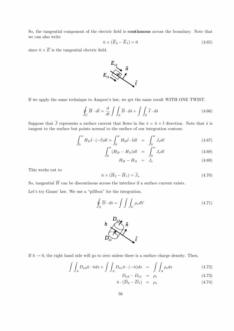
So, the tangential component of the electric field is continuous across the boundary. Note thatwe can also write
n× (E2 − E1) = 0 (4.65)
since n× E is the tangential electric field.
n
t
w1tE
2tEn
t
w1tE
2tE
If we apply the same technique to Ampere’s law, we get the same result WITH ONE TWIST.∮
CH · d` =
d
dt
∫ ∫
SB · ds +
∫ ∫
SJ · ds (4.66)
Suppose that J represents a surface current that flows in the s = n × t direction. Note that s istangent to the surface but points normal to the surface of our integration contour.
∫ w
0H1tt · (−t)d` +
∫ w
0H2tt · td` =
∫ w
0Jsd` (4.67)
∫ w
0(H2t −H1t)d` =
∫ w
0Jsd` (4.68)
H2t −H1t = Js (4.69)
This works out ton× (H2 −H1) = Js (4.70)
So, tangential H can be discontinous across the interface if a surface current exists.
Let’s try Gauss’ law. We use a “pillbox” for the integration.∮
SD · ds =
∫ ∫ ∫
VρvdV (4.71)
n
t1nD
2nDh n
t1nD
2nDh
If h → 0, the right hand side will go to zero unless there is a surface charge density. Then,∫ ∫
ADn2n · nds +
∫ ∫
ADn1n · (−n)ds =
∫ ∫
Aρsds (4.72)
Dn2 −Dn1 = ρs (4.73)n · (D2 −D1) = ρs (4.74)
56

So normal D is discontinous by the surface charge density. For magnetic fields:
Bn2 −Bn1 = 0 (4.75)n · (B2 −B1) = 0 (4.76)
Normal B is continous. Let’s summarize:
Field Two Dielectrics Dielectric ConductorTangential E Continuous Continous: n×E = 0Tangential H Continuous Discontinous: n×H1 = 0, n×H2 = Js
Normal D Continuous Discontinous: n ·D1 = 0, n ·D2 = ρs
Normal B Continuous Continous: n ·B = 0
57