transistors and layout - pearsonhighered.com need to study fabrication processes and the design...
TRANSCRIPT
33
2
Transistors and Layout
2.1 Introduction
We will start our study of VLSI design by learning about transistors and wiresand how they are fabricated. The basic properties of transistors are clearlyimportant for logic design. Going beyond a minimally-functional logic circuitto a high-performance design requires the consideration of
parasitic circuitelements
—capacitance and resistance. Those parasitics are created as neces-sary by-products of the fabrication process which creates the wires and tran-sistors, which gives us a very good reason to understand the basics of howintegrated circuits are fabricated. We will also study the rules which must beobeyed when designing the masks used to fabricate a chip and the basics oflayout design.
Our first step is to understand the basic fabrication techniques as described inSection 2.2. This material will describe how the basic structures for transistorsand wires are made. We will then study transistors and wires, both as inte-grated structures and as circuit elements, in Section 2.3 and Section 2.4,respectively. We will study design rules for layout in Section 2.5. Finally, wewill introduce some basic concepts and tools for layout design in Section 2.6.
34 Transistors and Layout
2.2 Fabrication Processes
We need to study fabrication processes and the design rules that govern lay-out. Examples are always helpful. We will use as our example the SCMOSrules, which have been defined by MOSIS, the MOS Implementation Service.(MOSIS is supported by the United States National Science Foundation. Simi-lar services, such as EuroChip/EuroPractice in the European Community,VDEC in Japan, and CIC in Taiwan, serve educational VLSI needs in othercountries.) SCMOS is unusual in that it is not a single fabrication process, buta collection of rules that hold for a family of processes. Using generic technol-ogy rules gives greater flexibility in choosing a manufacturer for your chips. Italso means that the SCMOS technology is less aggressive than any particularfabrication process developed for some special purpose—some manufactur-ers may emphasize transistor switching speed, for example, while othersemphasize the number of layers available for wiring. We will point outadvanced technology features that are not part of the SCMOS specificationbut may be found in a particular fabrication process.
2.2.1 Overview
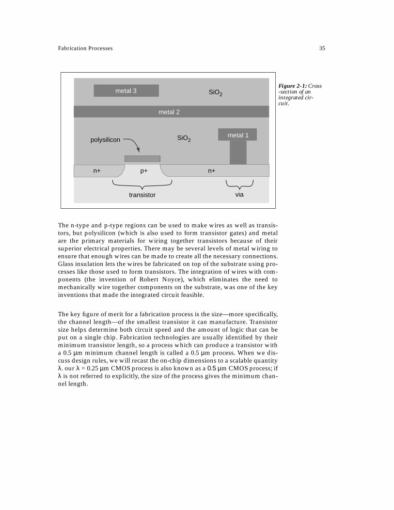
A cross-section of an integrated circuit is shown in Figure 2-1. Integrated cir-cuits are built on a silicon
substrate
. Components are formed by a combina-tion of processes:
•
doping
the substrate with impurities to create areas such as the n+and p+ regions;
• adding or cutting away insulating glass (
silicon dioxide
, or SiO
2
) ontop of the substrate;
• adding wires made of polycrystalline silicon (
polysilicon
, alsoknown as
poly
) or metal, insulated from the substrate by SiO
2
.
A pure silicon substrate contains equal numbers of two types of electrical car-riers: electrons and holes. While we will not go into the details of device phys-ics here, it is important to realize that the interplay between electrons andholes is what makes transistors work. The goal of doping is to create twotypes of regions in the substrate: an
n-type
region which contains primarilyelectrons and a
p-type
region which is dominated by holes. (Heavily dopedregions are referred to as n+ and p+.) Transistor action occurs at properlyformed boundaries between n-type and p-type regions.
Fabrication Processes 35
The n-type and p-type regions can be used to make wires as well as transis-tors, but polysilicon (which is also used to form transistor gates) and metalare the primary materials for wiring together transistors because of theirsuperior electrical properties. There may be several levels of metal wiring toensure that enough wires can be made to create all the necessary connections.Glass insulation lets the wires be fabricated on top of the substrate using pro-cesses like those used to form transistors. The integration of wires with com-ponents (the invention of Robert Noyce), which eliminates the need tomechanically wire together components on the substrate, was one of the keyinventions that made the integrated circuit feasible.
The key figure of merit for a fabrication process is the size—more specifically,the channel length—of the smallest transistor it can manufacture. Transistorsize helps determine both circuit speed and the amount of logic that can beput on a single chip. Fabrication technologies are usually identified by theirminimum transistor length, so a process which can produce a transistor witha 0.5
µ
m minimum channel length is called a 0.5
µ
m process. When we dis-cuss design rules, we will recast the on-chip dimensions to a scalable quantity
λ
. our
λ
= 0.25
µ
m CMOS process is also known as a
0.5 µ
m CMOS process; if
λ
is not referred to explicitly, the size of the process gives the minimum chan-nel length.
n+ n+p+
polysilicon
metal 3
metal 2
metal 1
transistor via
SiO2
SiO2
Figure 2-1: Cross-section of an integrated cir-cuit.

36 Transistors and Layout
2.2.2 Fabrication Steps
Features are patterned on the wafer by a photolithographic process; the waferis covered with light-sensitive material called
photoresist
, which is thenexposed to light with the proper pattern. The patterns left by the photoresistafter development can be used to control where SiO
2
is grown or materials areplaced on the surface of the wafer.
A layout contains summary information about the patterns to be made on thewafer. Photolithographic processing steps are performed using
masks
whichare created from the layout information supplied by the designer. In simpleprocesses there is roughly one mask per layer in a layout, though in morecomplex processes some masks may be built from several layers while onelayer in the layout may contribute to several masks. Figure 2-2 shows a sim-ple layout and the mask used to form the polysilicon pattern.
layout
poly mask
metal
metal-poly via
diffusion
poly
Figure 2-2: The relationship between layouts and fabrication masks.
Fabrication Processes 37
Transistors are fabricated within regions called
tubs
or
wells
: an n-type tran-sistor is built in a p-tub, and a p-type transistor is built in an n-tub. The wellsprevent undesired conduction from the drain to the substrate. (Rememberthat the transistor type refers to the minority carrier which forms the inver-sion layer, so an n-type transistor pulls electrons out of a p-tub.) There arethree ways to form tubs in a substrate:
• start with a p-doped wafer and add n-tubs;
• start with an n-doped wafer and add p-tubs;
• start with an undoped wafer and add both n- and p-tubs.
CMOS processes were originally developed from nMOS processes, which usep-type wafers into which n-type transistors are added. However, the
twin-tub process
, which uses an undoped wafer, has become the most commonlyused process because it produces tubs with better electrical characteristics.We will therefore use a twin-tub process as an example.
Figure 2-3 illustrates important steps in a twin-tub process. Details can varyfrom process to process, but these steps are representative. The first step is toput tubs into the wafer at the appropriate places for the n-type and p-typewafers. Regions on the wafer are selectively doped by implanting ionizeddopant atoms into the material, then heating the wafer to heal damagecaused by ion implantation and further move the dopants by diffusion. Thetub structure means that n-type and p-type wires cannot directly connect.Since the two diffusion wire types must exist in different type tubs, there is noway to build a via which can directly connect them. Connections must bemade by a separate wire, usually metal, which runs over the tubs.
The next steps form an oxide covering of the wafer and the polysilicon wires.The oxide is formed in two steps: first, a thick field oxide is grown over theentire wafer. The field oxide is etched away in areas directly over transistors;a separate step grows a much thinner oxide which will form the insulator ofthe transistor gates. After the field and thin oxides have been grown, the pol-ysilicon wires are formed by depositing polysilicon crystalline directly on theoxide.
Note that the polysilicon wires have been laid down before the diffusionwires were made—that order is critical to the success of MOS processing. Dif-fusion wires are laid down immediately after polysilicon deposition to create
self-aligned
transistors—the polysilicon masks the formation of diffusionwires in the transistor channel. For the transistor to work properly, there must
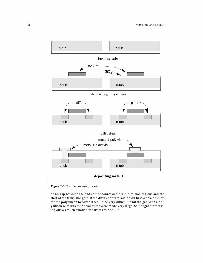
38 Transistors and Layout
be no gap between the ends of the source and drain diffusion regions and thestart of the transistor gate. If the diffusion were laid down first with a hole leftfor the polysilicon to cover, it would be very difficult to hit the gap with a pol-ysilicon wire unless the transistor were made very large. Self-aligned process-ing allows much smaller transistors to be built.
Figure 2-3: Steps in processing a wafer.
forming tubs
depositing polysilicon
depositing metal 1
diffusion
p-tub n-tub
p-tub n-tub
poly
SiO2
p-tub n-tub
n diff p diff
metal 1-n diff via
p-tub n-tub
metal 1-poly via

Transistors 39
After the diffusions are complete, another layer of oxide is deposited to insu-late the polysilicon and metal wires. Although copper wires promise to pro-vide substantially lower-resistance wires, at this writing metal connectionsare made using aluminum. Holes are cut in the field oxide where vias aredesired, then metal 1 is deposited where desired. The metal fills the cuts tomake connections between layers. The metal 2 layer requires an additionaloxidation/cut/deposition sequence. After all the important circuit featureshave been formed, the chip is covered with a final
passivation layer
of SiO
2
to protect the chip from chemical contamination.
2.3 Transistors
2.3.1 Structure of the Transistor
Figure 2-4 shows the cross-section of an n-type MOS transistor. (The nameMOS is an anachronism. The first such transistors used a metal wire for agate, making the transistor a sandwich of metal, silicon dioxide, and the semi-conductor substrate. Even though transistor gates are now made of polysili-con, the name MOS has stuck.) An n-type transistor is embedded in a p-typesubstrate; it is formed by the intersection of an n-type wire and a polysiliconwire. The region at the intersection, called the
channel
, is where the transis-tor action takes place. The channel connects to the two n-type wires whichform the source and drain, but is itself doped to be p-type. The insulating sili-con dioxide at the channel (called the
gate oxide
) is much thinner than it isaway from the channel (called the
field oxide
); having a thin oxide at thechannel is critical to the successful operation of the transistor.
source (n+) drain (n+)channel
substrate (p)
SiO2
L
Wpoly
Figure 2-4: Cross-section of an n-type transistor.
40 Transistors and Layout
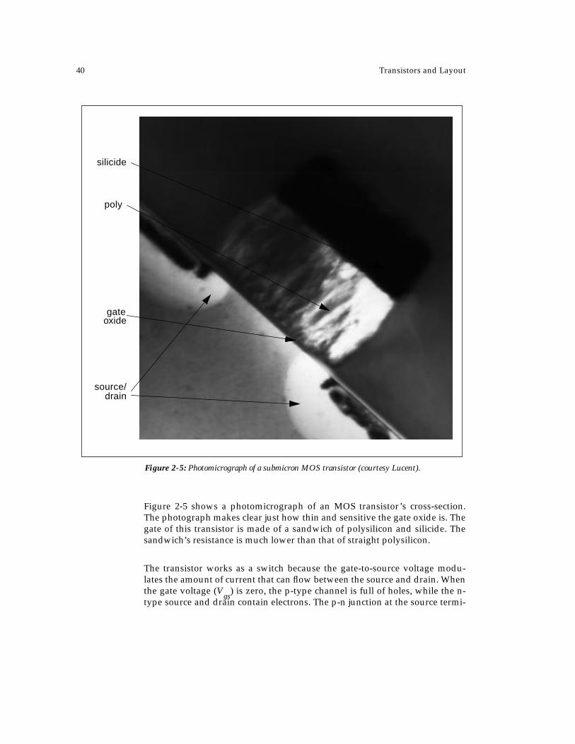
Figure 2-5 shows a photomicrograph of an MOS transistor’s cross-section.The photograph makes clear just how thin and sensitive the gate oxide is. Thegate of this transistor is made of a sandwich of polysilicon and silicide. Thesandwich’s resistance is much lower than that of straight polysilicon.
The transistor works as a switch because the gate-to-source voltage modu-lates the amount of current that can flow between the source and drain. Whenthe gate voltage (
V
gs
) is zero, the p-type channel is full of holes, while the n-type source and drain contain electrons. The p-n junction at the source termi-
gate
poly
silicide
source/drain
Figure 2-5: Photomicrograph of a submicron MOS transistor (courtesy Lucent).
oxide

Transistors 41
nal forms a diode, while the junction at the drain forms a second diode thatconducts in the opposite direction. As a result, no current can flow from thesource to the drain.
As
V
gs
rises above zero, the situation starts to change. While the channelregion contains predominantly p-type carriers, it also has some n-type carri-ers. The positive voltage on the polysilicon which forms the gate attracts theelectrons. Since they are stopped by the gate oxide, they collect at the top ofthe channel along the oxide boundary. At a critical voltage called the
thresh-old voltage
(
V
t
), enough electrons have collected at the channel boundary toform an
inversion layer
—a layer of electrons dense enough to conduct cur-rent between the source and the drain.
The size of the channel region is labeled relative to the direction of currentflow: the channel
length
(
L
) is along the direction of current flow betweensource and drain, while the
width
(
W
) is perpendicular to current flow. Theamount of current flow is a function of the
W
/
L
ratio, for the same reasonsthat bulk resistance changes with the object’s width and length: widening thechannel gives a larger cross-section for conduction, while lengthening thechannel increases the distance current must flow through the channel. Sincewe can choose
W
and
L
when we draw the layout, we can very simply designthe transistor current magnitude.
P-type transistors have identical structures but complementary materials:trade p’s and n’s in Figure 2-4 and you have a picture of a p-type transistor.The p-type transistor conducts by forming an inversion region of holes in then-type channel; therefore, the gate-to-source voltage must be negative for thetransistor to conduct current.
42 Transistors and Layout
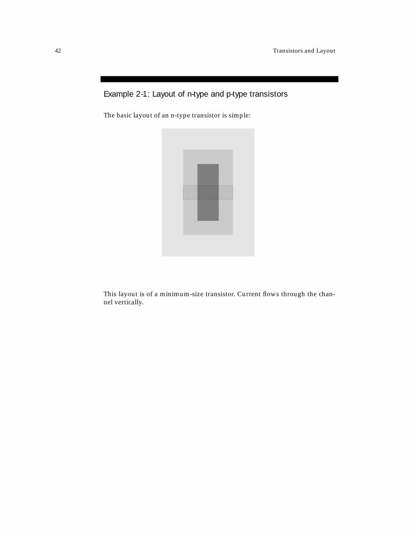
Example 2-1: Layout of n-type and p-type transistors
The basic layout of an n-type transistor is simple:
This layout is of a minimum-size transistor. Current flows through the chan-nel vertically.

Transistors 43
The layout of a p-type transistor is very similar:
In both cases, the tub rectangles are added as required. The details of whichtub must be specified vary from process to process; many designers use sim-ple programs to generate the tubs required around rectangles.
Fabrication engineers may sometimes refer to the
drawn length
of a transis-tor. Photolithography steps may affect the length of the channel. As a result,the actual channel length may not be the drawn length. The drawn length isusually the parameter of interest to the digital designer, since that is the sizeof rectangle that must be used to get a transistor of the desired size.

44 Transistors and Layout
We can also draw a wider n-type transistor, which delivers more current:
2.3.2 A Simple Transistor Model
The behavior of both n-type and p-type transistors is described by two equa-tions and two physical constants; the sign of one of the constants distin-guishes the two types of transistors. The variables that describe a transistor’sbehavior, some of which we have already encountered, are:
•
V
gs
—the gate-to-source voltage;
•
V
ds
—the drain-to-source voltage (remember that
V
ds
= -
V
sd
);
•
I
d
—the current flowing between the drain and source.
The constants that determine the magnitude of source-to-drain current in thetransistor are:
•
V
t
—the transistor threshold voltage, which is positive for an n-type
Transistors 45
transistor and negative for a p-type transistor;
•
k
’—the transistor transconductance, which is positive for both typesof transistors;
•
W
/
L—
the width-to-length ratio of the transistor.
Both
V
t
and
k
’ are measured, either directly or indirectly, for a fabrication pro-cess.
W
/
L
is determined by the layout of the transistor, but since it does notchange during operation, it is a constant of the device equations.
The equations that govern the transistor’s behavior are traditionally writtento show the drain current as a function of the other parameters. A reasonablyaccurate model for the transistor’s behavior, written in terms of the drain cur-rent
I
d
, divides operation into
linear
and
saturated
[Yan78]. For an n-typetransistor, we have:
•
Linear region
:
(EQ 2-1)
•
Saturated region
:
VDS
saturationlinear
VGS = 1.5V
VGS = 2.5V
VGS = 5VID
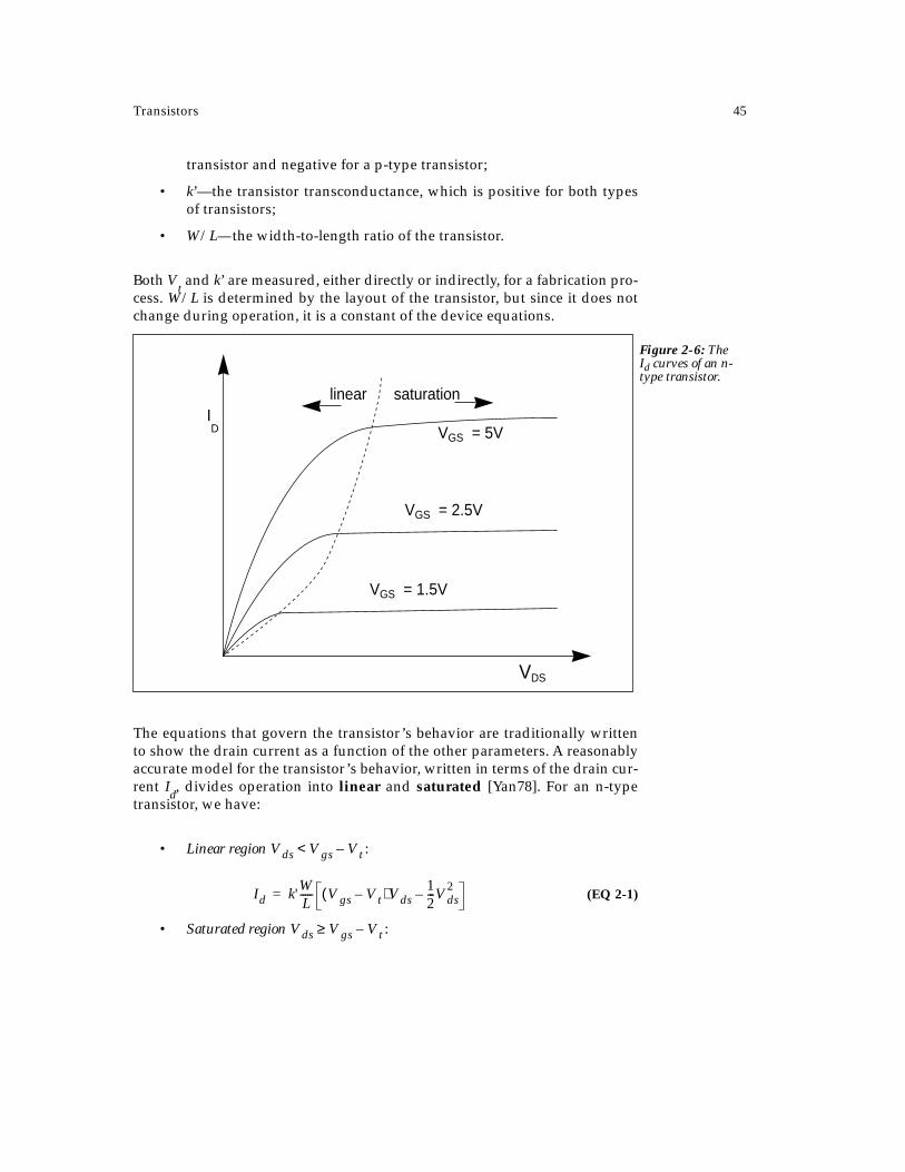
Figure 2-6: The Id curves of an n-type transistor.
Vds Vgs Vt–<
Id k'WL----- Vgs Vt–( )Vds
12---Vds
2–=
Vds Vgs Vt–≥
46 Transistors and Layout
(EQ 2-2)
For a p-type transistor, the drain current is negative and the device is on whenVgs is below the device’s negative threshold voltage. Figure 2-6 plots theseequations over some typical values for an n-type device. Each curve showsthe transistor current as Vgs is held constant and Vds is swept from 0 V to alarge voltage.
The transistor’s switch action occurs because the density of carriers in thechannel depends strongly on the gate-to-substrate voltage. For ,there are not enough carriers in the inversion layer to conduct an appreciablecurrent. (To see how much current is conducted in the subthreshold region,check Section 2.3.5.) Beyond that point and until saturation, the number ofcarriers is directly related to Vgs: the greater the gate voltage applied, themore carriers are drawn to the inversion layer and the greater the transistor’sconductivity.
The relationship between W/L and source-drain current is equally simple. Asthe channel width increases, more carriers are available to conduct current. Aschannel length increases, however, the drain-to-source voltage diminishes ineffect. Vds is the potential energy available to push carriers from drain tosource; as the distance from drain to source increases, it takes longer to pushcarriers across the transistor for a fixed Vds, reducing current flow.
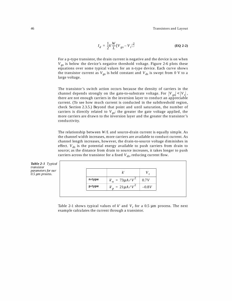
Table 2-1 shows typical values of k’ and Vt for a 0.5 µm process. The nextexample calculates the current through a transistor.
Id12---k'W
L----- Vgs Vt–( )2
=
Vgs Vt<
n-type
p-type
k' Vt
k'n 73µA V2⁄= 0.7V
k'p 21µA V2⁄= 0.8V–
Table 2-1 Typical transistor parameters for our 0.5 µm process.

Transistors 47
Example 2-2: Current through a transistor
A minimum-size transistor in the SCMOS rules is formed by a L = 2 λ and W= 3 λ. Given this size of transistor and the 0.5 µm transistor characteristics, thecurrent through a minimum-sized n-type transistor at the boundary betweenthe linear and saturation regions when the gate is at the low voltage
would be
.
The saturation current when the transistor’s gate is connected to a 5 V powersupply would be
.
2.3.3 Transistor Parasitics
Real devices have parasitic elements which are necessary artifacts of thedevice structure. Since the transistor is a non-linear device, we are primarilyconcerned with its capacitances as parasitics, although the source and drainregions have significant resistance.
The transistor itself introduces significant gate capacitance, Cg. This capaci-
tance, which comes from the parallel plates formed by the poly gate and thesubstrate, forms the majority of the capacitive load in small logic circuits;
for both n-type and p-type transistors in a typical 2 µm pro-cess. The total gate capacitance for a transistor is computed by measuring thearea of the active region (or W × L) and multiplying the area by the unitcapacitance C
g. We don’t worry about fringing because the edges of the gate
are capacitively coupled to the source and drain and the total gate capaci-
Vgs 2V=
Id12--- 73
µA
V2--------
3µm2µm------------
2V 0.7V–( )293µA= =
Id12--- 73
µAV
-------- 3µm
2µm------------
5V 0.7V–( )21.0mA= =
Cg 0.9fF µm2⁄=

48 Transistors and Layout
tance contributed by all sources remains relatively constant throughout thetransistor’s operating regime.
We may, however, want to worry about the source/drain overlap capaci-tances. During fabrication, the dopants in the source/drain regions diffuse inall directions, including under the gate as shown in Figure 2-7. Thesource/drain overlap region tends to be a larger fraction of the channel areain deep submicron devices. The overlap region is independent of the transis-tor length, so it is usually given in units of Farads per unit gate width. Thenthe total source overlap capacitance for a transistor would be
. (EQ 2-3)
There is also a gate/bulk overlap capacitance due to the overhang of thegate past the channel and onto the bulk.
The source and drain regions also have a non-trivial capacitance to the sub-strate and a very large resistance. Circuit simulation may require the specifi-cation of source/drain capacitances and resistances. However, the techniquesfor measuring the source/drain parasitics at the transistor are the same asthose used for measuring the parasitics of long diffusion wires. Therefore, wewill defer the study of how to measure these parasitics to Section 2.4.1.
2.3.4 Tub Ties and Latchup
An MOS transistor is actually a four-terminal device, but we have up to nowignored the electrical connection to the substrate. The substrates underneaththe transistors must be connected to a power supply: the p-tub (which con-tains n-type transistors) to V
SS and the n-tub to V
DD. These connections are
made by special vias called tub ties.
source drain
Cgs Cgd
overlap
Figure 2-7: Para-sitic capacitances from the gate to the source/drain-overlap regions.
Cgs ColW=

Transistors 49
Figure 2-8 shows the cross-section of a tub tie connecting to an n-tub and Fig-ure 2-9 shows a tub tie next to a via and an n-type transistor. The tie connectsa metal wire connected to the V
DD power supply directly to the substrate.
The connection is made through a standard via cut. The substrate underneath
Figure 2-8: Cross-sec-tion of an n-tub tie.
n-tub
n+
substrate
metal 1 (VDD)
oxide
Figure 2-9: A layout sec-tion featuring a tub tie.
tub tie
via

50 Transistors and Layout
the tub tie is heavily doped with n-type dopants (denoted as n+) to make alow-resistance connection to the tub. The SCMOS rules make the conservativesuggestion that tub ties be placed every one to two transistors. Other pro-cesses may relax that rule to allow tub ties every four to five transistors. Whynot place one tub tie in each tub—one tub tie for every 50 or 100 transistors?Using many tub ties in each tub makes a low-resistance connection betweenthe tub and the power supply. If that connection has higher resistance, para-sitic bipolar transistors can cause the chip to latch-up, inhibiting normal chipoperation.
Figure 2-10 shows a chip cross-section which might be found in an inverter orother logic gate. The MOS transistor and tub structures form parasitic bipolartransistors: npn transistors are formed in the p-tub and pnp transistors in then-tub. Since the tub regions are not physically isolated, current can flowbetween these parasitic transistors along the paths shown as wires. Since thetubs are not perfect conductors, some of these paths include parasitic resis-tors; the key resistances are those between the power supply terminals andthe bases of the two bipolar transistors.
The parasitic bipolar transistors and resistors create a parasitic silicon-con-trolled rectifier, or SCR. The schematic for the SCR and its behavior areshown in Figure 2-11. The SCR has two modes of operation. When both bipo-lar transistors are off, the SCR conducts essentially no current between its twoterminals. As the voltage across the SCR is raised, it may eventually turn onand conducts a great deal of current with very little voltage drop. The SCRformed by the n- and p-tubs, when turned on, forms a high-current, low-volt-
Figure 2-10: Parasitics which cause latch-up.
p-tub n-tub
VDDVSS
RW
RS
n+ p+
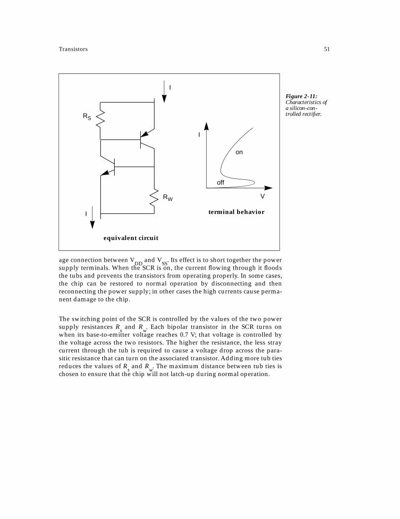
Transistors 51
age connection between VDD
and VSS
. Its effect is to short together the powersupply terminals. When the SCR is on, the current flowing through it floodsthe tubs and prevents the transistors from operating properly. In some cases,the chip can be restored to normal operation by disconnecting and thenreconnecting the power supply; in other cases the high currents cause perma-nent damage to the chip.
The switching point of the SCR is controlled by the values of the two powersupply resistances R
s and R
w. Each bipolar transistor in the SCR turns on
when its base-to-emitter voltage reaches 0.7 V; that voltage is controlled bythe voltage across the two resistors. The higher the resistance, the less straycurrent through the tub is required to cause a voltage drop across the para-sitic resistance that can turn on the associated transistor. Adding more tub tiesreduces the values of R
s and R
w. The maximum distance between tub ties is
chosen to ensure that the chip will not latch-up during normal operation.
equivalent circuit
terminal behavior
RW
RS
I
I
I
V
off
on
Figure 2-11: Characteristics of a silicon-con-trolled rectifier.

52 Transistors and Layout
2.3.5 Advanced Transistor Characteristics
In order to better understand the transistor, we will derive the basic devicecharacteristics that were stated in Section 2.3.2. Along the way we will be ableto identify some second-order effects that can become significant when we tryto optimize a circuit design.
The parallel place capacitance of the gate determines the characteristics of thechannel. We know from basic physics that the parallel-plate oxide capacitanceper unit area (in units of Farads per cm2) is
, (EQ 2-4)
where is the permittivity of silicon dioxide (about 3.9ε0, where ε0, the per-mittivity of free space, is ) and xox is the oxide thickness incentimeters.
The intrinsic carrier concentration of silicon is denoted as . N-type dopingconcentrations are written as (donor) while p-type doping concentrationsare written as (acceptor). Table 2-2 gives the values of some importantphysical constants.
Applying a voltage of the proper polarity between the gate and substratepulls minority carriers to the lower plate of the capacitor, namely the channelregion near the gate oxide. The threshold voltage is defined as the voltage atwhich the number of minority carriers (electrons in an n-type transistor) inthe channel region equals the number of majority carriers in the substrate.(This actually defines the strong threshold condition.) So the threshold volt-age may be computed from the component voltages which determine the
Cox εox xox⁄=
εox8.854 10
14–× F cm⁄
Table 2-2 Values of some physical constants.
charge of an electron q
Si intrinsic carrier concentration ni
permittivity of free space
permittivity of Si
thermal voltage (300K) kT/q
1.6 1019–× C
1.45 1012C cm3⁄×
ε0 8.854 1014– F cm2⁄×
εSi 3.9ε0
0.026V
niNd
Na

Transistors 53
number of carriers in the channel. The threshold voltage (assuming that thesource/substrate voltage is zero) has four major components:
. (EQ 2-5)
Let us consider each of these terms.
• The first component, , is the flatband voltage, which in modernprocesses has two main components:
(EQ 2-6)
is the difference in work functions between the gate and sub-strate material, while Qf is the fixed surface charge. (Trapped chargeused to be a significant problem in MOS processing which increasedthe flatband voltage and therefore the threshold voltage. However,modern processing techniques control the amount of trappedcharge.)
If the gate polysilicon is n-doped at a concentration of Ndp, the for-mula for the work function difference is
. (EQ 2-7)
If the gate is p-doped at a concentration of Nap, the work function dif-ference is
. (EQ 2-8)
• The second term is the surface potential. At the threshold voltage, thesurface potential is twice the Fermi potential of the substrate:
. (EQ 2-9)
• The third component is the voltage across the parallel plate capacitor.The value of the charge on the capacitor is
. (EQ 2-10)
Vt0 V fb φsQbCox--------- VII+ + +=
V fb
V fb Φgs Q f Cox⁄–=
Φgs
ΦgskTq
------ lnNaNdp
ni2
-----------------
–=
ΦgskTq
------ lnNapNa---------
=
φs 2 φF≈ 2kTq
------ lnNani------=
Qb
2qεsiNaφs

54 Transistors and Layout
(We will not derive this value, but the square root comes from thevalue for the depth of the depletion region.)
• An additional ion implantation step is also performed to adjust thethreshold voltage—the fixed charge of the ions provides a bias volt-age on the gate. The voltage adjustment has the value ,where is the ion implantation concentration; the voltage adjust-ment may be positive or negative, depending on the type of ionimplanted.
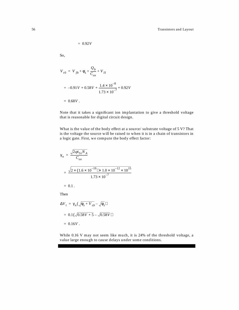
When the source/substrate voltage is not zero, we must add another term tothe threshold voltage. Variation of threshold voltage with source/substratevoltage is called body effect, which can significantly affect the speed of com-plex logic gates. The amount by which the threshold voltage is increased is
(EQ 2-11)
The term is the body effect factor, which depends on the gate oxide thick-ness and the substrate doping:
. (EQ 2-12)
(To compute , we substitute the n-tub doping ND for NA.) We will see howbody effect must be taken into account when designing logic gates inSection 3.3.4.
Example 2-3: Threshold voltage of a transistor
First, we will calculate the value of the threshold voltage of an n-type transis-tor at zero source/substrate bias. First, some reasonable values for the param-eters:
• ;
• ;
• ;
VII qDI Cox⁄DI
Vt∆ γn φs Vsb+ φs–( )=
γn
γn2qεSiNA
Cox--------------------------=
γp
xox 200A°=
εox 3.5 1013–× F cm⁄=
φs 0.6V=

Transistors 55
• ;
• ;
• NA = 1015 cm-3;
• Nap = 1019 cm-3;
• .
Let’s compute each term of :
•
.
•
•
.
•
•
•
Q f q 1011× 1.6 10
8–× F cm2⁄= =
εsi 1.0 1012–×=
NII 1 1012×=
Vt0
Cox εox xox⁄=
3.45 1013–× 2 10
6–×⁄ 1.73 107–× F cm2⁄= =
ΦgskTq
------ lnNaNdp
ni2
-----------------
–=
0.02610
1510
19
1.45 1010×( )
2-----------------------------------
–=
0.82V–=
V fb Φgs Q f Cox⁄+=
0.82– 1.6 108–× 1.73 10
7–×⁄–=
˙ 0.91– V=
φs 2kTq
------ lnNani------=
2 0.026 ln10
15
1.45 1010×
---------------------------
××=
0.58V=
Qb 2qεsiNaφs=
2 1.6 1019–×( ) 1.0 10
12–× 1015
0.58××××=
1.4 108–×=
VII qDI Cox⁄=
1.6 1019–×( ) 1 10
12×( )× 1.73 107–×( )⁄=
56 Transistors and Layout
So,
.
Note that it takes a significant ion implantation to give a threshold voltagethat is reasonable for digital circuit design.
What is the value of the body effect at a source/substrate voltage of 5 V? Thatis the voltage the source will be raised to when it is in a chain of transistors ina logic gate. First, we compute the body effect factor:
.
Then
.
While 0.16 V may not seem like much, it is 24% of the threshold voltage, avalue large enough to cause delays under some conditions.
0.92V=
Vt0 V fb φsQbCox--------- VII+ + +=
0.91– V 0.58V 1.4 108–×
1.73 107–×
---------------------------- 0.92V+ + +=
0.68V=
γn2qεSiNA
Cox--------------------------=
2 1.6 1019–×( ) 1.0 10
12–× 1015×××
1.73 107–×
------------------------------------------------------------------------------------------------=
0.1=
Vt∆ γn φs Vsb+ φs–( )=
0.1 0.58V 5+ 0.58V–( )=
0.16V=
Transistors 57
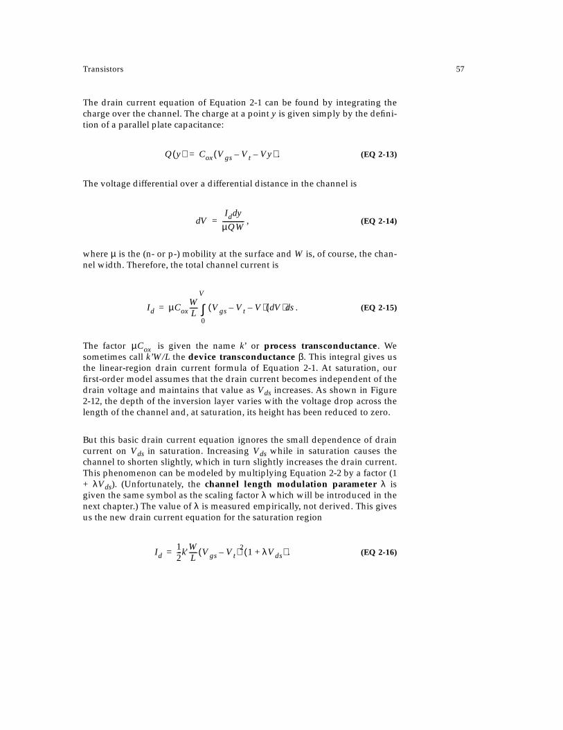
The drain current equation of Equation 2-1 can be found by integrating thecharge over the channel. The charge at a point y is given simply by the defini-tion of a parallel plate capacitance:
. (EQ 2-13)
The voltage differential over a differential distance in the channel is
, (EQ 2-14)
where µ is the (n- or p-) mobility at the surface and W is, of course, the chan-nel width. Therefore, the total channel current is
. (EQ 2-15)
The factor is given the name k’ or process transconductance. Wesometimes call k’W/L the device transconductance β. This integral gives usthe linear-region drain current formula of Equation 2-1. At saturation, ourfirst-order model assumes that the drain current becomes independent of thedrain voltage and maintains that value as Vds increases. As shown in Figure2-12, the depth of the inversion layer varies with the voltage drop across thelength of the channel and, at saturation, its height has been reduced to zero.
But this basic drain current equation ignores the small dependence of draincurrent on Vds in saturation. Increasing Vds while in saturation causes thechannel to shorten slightly, which in turn slightly increases the drain current.This phenomenon can be modeled by multiplying Equation 2-2 by a factor (1+ λVds). (Unfortunately, the channel length modulation parameter λ isgiven the same symbol as the scaling factor λ which will be introduced in thenext chapter.) The value of λ is measured empirically, not derived. This givesus the new drain current equation for the saturation region
. (EQ 2-16)
Q y( ) Cox Vgs Vt Vy––( )=
VdId yd
µQW--------------=
Id µCoxWL----- Vgs Vt– V–( ) Vd( ) sd
0
V
∫=
µCox
Id12---k'W
L----- Vgs Vt–( )2
1 λVds+( )=

58 Transistors and Layout
Unfortunately, the λ term causes a slight discontinuity between the drain cur-rent equations in the linear and saturation regions—at the transition point,the λVds term introduces a small jump in Id. A discontinuity in drain currentis clearly not physically possible, but the discontinuity is small and usuallycan be ignored during manual analysis of the transistor’s behavior. Circuitsimulation, however, may require using a slightly different formulation thatkeeps drain current continuous.
It is also possible to model the subthreshold conduction of the transistor—thecurrent carried when the gate voltage is below the threshold. The thresholdvoltage is chosen somewhat arbitrarily and the transistor does carry a verysmall current. Furthermore, that current drops off exponentially as the gatevoltage decreases as shown in Figure 2-13. We can derive the subthresholdcurrent by modeling the device as a bipolar transistor [Sze85], since the draincurrent is dominated by diffusion, not drift. In this case, the channel forms avery wide base for the bipolar transistor.
source (n+)
current
drain (n+)
inversionlayer
source (n+)
current
drain (n+)
source (n+)
current
drain (n+)
Vgs Vt<Figure 2-12: Shape of the inversion layer as a function of gate voltage.
Vgs Vt=
Vgs Vt>
Transistors 59
Then the current through the channel is
. (EQ 2-17)
In this formula, Dn is the diffusion coefficient, A is the area of the channelcross section (perpendicular to current flow). n(0) and n(L) are the electrondensities at the source and drain, whose values are:
, (EQ 2-18)
. (EQ 2-19)
By substituting into Equation 2-17, we can see that the subthreshold current isin fact an exponential function of threshold voltage. We also see that the sub-threshold current is temperature-dependent.
The relationship between Id and Vgs is approximately
(EQ 2-20)
subthreshold
10-8
10-7
10-6
10-5
ln Id
Vgs
Figure 2-13: Characteristics of subthreshold cur-rent.
Id qADnndyd
------– qADnn 0( ) n L( )–
L-----------------------------–= =
n 0( ) nieq ΨS ΨB–( ) kT⁄( )
=
n 0L( ) nieq ΨS ΨB Vd––( ) kT⁄( )
=
Vgsdd Idln
1– kTq
------ 10 1 α+( )ln=
60 Transistors and Layout
where α is a physical constant greater than 1. The details of subthreshold con-duction are not important for most digital circuits. However, the fact that thetransistor is not a perfect switch with infinite off impedance affects the designof dynamic gates because the subthreshold current changes the charge storedin the gate.
In contrast to the subthreshold drain current, leakage currents flow from thesource or drain to the substrate. The source/drain and the substrate form adiode which conducts whenever the voltage across the diode is non-zero. Thegeneral form of the leakage current comes from the diode current law:
. (EQ 2-21)
Il0 is the reverse saturation current, typically on the order of a few tenths of ananoamp. Leakage currents are the source of static power dissipation in prop-erly-designed CMOS circuits, as we will see in Section 3.3.5.
2.3.6 Advanced Transistor Structures
The modern MOS transistor is more complex than the basic transistor shownin Figure 2-4. A number of improvements to the basic MOS structure havebeen introduced over time to increase performance and permit the construc-tion of efficient, short-channel devices [Bre90]. These new structures increaseprocess complexity. The region between the source and drain is more heavilydoped than the region underneath, allowing the source and drain to be putcloser together. An epitaxial layer—a crystalline layer grown on top of thewafer during processing—allows fine control of doping in large regions; thelightly-doped region created underneath the source and drain by epitaxialgrowth reduces the junction capacitance between the two. The contacts to thesource and drain are also designed to reduce source/drain capacitance byreducing the contact area. The diffusion is made thin near the channel area toreduce the penetration of the source/drain electric fields into the channelarea. Many transistors also use lightly-doped drains to reduce the generationof hot electrons—high-energy electrons which can physically damage thedrain region. We saw a silicided poly gate in Figure 2-5; silicides can also beapplied to diffusions to reduce their resistance.
Il Il0 eVd kT⁄
1–( )=

Transistors 61
2.3.7 Spice Models
A circuit simulator, of which Spice [Nag75] is the prototypical example, pro-vides the most accurate description of system behavior by solving for volt-ages and currents over time. The basis for circuit simulation is Kirchoff’slaws, which describe the relationship between voltages and currents. Linearelements, like resistors and capacitors, have constant values in Kirchoff’slaws, so the equations can be solved by standard linear algebra techniques.However, transistors are non-linear, greatly complicating the solution of thecircuit equations. The circuit simulator uses a model—an equivalent circuitwhose parameters may vary with the values of other circuits voltages andcurrents—to represent a transistor. Unlike linear circuits, which can be solvedanalytically, numerical solution techniques must be used to solve non-linearcircuits. The solution is generated as a sequence of points in time. Given thecircuit solution at time t, the simulator chooses a new time t+δ and solves forthe new voltages and currents. The difficulty of finding the t+δ solutionincreases when the circuit’s voltages and currents are changing very rapidly,so the simulator chooses the time step δ based on the derivatives of the Is andVs. The resulting values can be plotted in a variety of ways using interactivetools.
A circuit simulation is only as accurate as the model for the transistor. Mostversions of Spice offer three MOS transistor models, called naturally enoughlevel 1, level 2, and level 3 [Gei90, Rab96]. The level 1Spice model is roughlythe device equations of Section 2.3. The level 2Spice model provides moreaccurate determination of effective channel length and the transition betweenthe linear and saturation regions, but is used less frequently today. The level3Spice model uses empirical parameters to provide a better fit to the mea-sured device characteristics. Each model requires a number of parameterswhich should be supplied by your fabrication vendor. The level 4 model, alsoknown as the BSIM model, uses some extracted parameters, but is smallerand more efficient. Even more recent models, including level 28 (BSIM2) andlevel 47 (BSIM3) have been developed recently to more accurately modeldeep submicron transistors.
Table 2-3 gives the Spice names for some common parameters of Spice mod-els and their correspondence to names used in the literature. Process vendorstypically supply customers with Spice model parameters directly. You shoulduse these values rather than try to derive them from some other parameters.

62 Transistors and Layout
parameter symbol Spice name
channel drawn length L L
channel width W W
source, drain areas AS, AD
source, drain perimeters PS, PD
source/drain resistances Rs, Rd RS, RD
source/drain sheet resistance RSH
zero-bias bulk junction capacitance Cj0 CJ
bulk junction grading coefficient m MJ
zero-bias sidewall capacitance Cjsw0 CJSW
sidewall grading coefficient msw MJSW
gate-bulk/source/drain overlap capacitances Cgb0/Cgs0/Cgd0
CGBO, CGSO, CGDO
bulk junction leakage current Is IS
bulk junction leakage current density Js JS
bulk junction potential φ0 PB
zero-bias threshold voltage Vt0 VT0
transconductance k’ KP
body bias factor γ GAMMA
channel modulation λ LAMBDA
oxide thickness tox TOX
lateral diffusion xd LD
metallurgical junction depth xj XJ
surface inversion potential PHI
substrate doping NA, ND NSUB
surface state density Qss/q NSS
surface mobility µ0 U0
maximum drift velocity vmax VMAX
mobility critical field Ecrit UCRIT
critical field exponent in mobility degradation UEXP
type of gate material TPG
2 φF
Table 2-3 Names of some Spice parame-ters.

Wires and Vias 63
2.4 Wires and Vias
Figure 2-14 illustrates the cross-section of a nest of wires and vias. N-diffu-sion and p-diffusion wires are created by doping regions of the substrate. Pol-ysilicon and metal wires are laid over the substrate, with silicon dioxide toinsulate them from the substrate and each other. Wires are added in layers tothe chip, alternating with SiO
2: a layer of wires is added on top of the existing
silicon dioxide, then the assembly is covered with an additional layer of SiO2
to insulate the new wires from the next layer. Vias are simply cuts in the insu-lating SiO
2; the metal flows through the cut to make the connection on the
desired layer below. Figure 2-15 shows a photomicrograph of a multi-levelinterconnect structure, including four levels of metal and one level of polysil-icon.
In addition to carrying signals, metal lines are used to supply power through-out the chip. On-chip metal wires have limited current-carrying capacity, asdoes any other wire. (Poly and diffusion wires also have current limitations,but since they are not used for power distribution those limitations do notaffect design.) Electrons drifting through the voltage gradient on a metal linecollide with the metal grains which form the wire. A sufficiently high-energycollision can appreciably move the metal grain. Under high currents, electroncollisions with metal grains cause the metal to move; this process is calledmetal migration (also known as electromigration) [Mur93].
n+
substrate
metal 1
metal 2
poly
vias
oxide
Figure 2-14: A cross-section of a chip show-ing wires and vias.
64 Transistors and Layout
The mean time to failure (MTF) for metal wires—the time it takes for 50% oftesting sites to fail—is a function of current density:
, (EQ 2-22)
where j is the current density, n is a constant between 1 and 3, and Q is the dif-fusion activation energy. This equation is derived from the drift velocity rela-tionship.
Metal wires can handle 1.5 mA of current per micron of wire width under theSCMOS rules. (Width is measured perpendicular to current flow.) A 3 µmwire can handle 4.5 mA of current. We will see in Chapter 3 that 4.5 mA isenough current to supply a large number of logic gates, so in small designs,metal migration limits are not a major problem. In larger designs, however,sizing power supply lines is critical to ensuring that the chip does not failonce it is installed in the field.
Figure 2-15: Cross-section of 4-level metal/1-level poly interconnect (courtesy UMC).
MTF j n– eQ kT⁄∝

Wires and Vias 65
2.4.1 Wire Parasitics
Wires, vias and transistors all introduce parasitic elements into our circuits.Inductance is not a significant problem in current generations of integratedcircuit technology (though, as we will see in Chapter 7, it is an important con-cern in IC packaging), so the parasitics of interest are resistance and capaci-tance. It is important to understand the structural properties of ourcomponents that introduce parasitic elements, and how to measure parasiticelement values from layouts.
Diffusion wire capacitance is introduced by the p-n junctions at the bound-aries between the diffusion and underlying tub or substrate. While thesecapacitances change with the voltage across the junction, which varies duringcircuit operation, we generally assume worst-case values. An accurate mea-surement of diffusion wire capacitance requires separate calculations for thebottom and sides of the wire—the doping density, and therefore the junctionproperties, vary with depth. To measure total capacitance, we measure thediffusion area, called bottomwall capacitance, and perimeter, called side-wall capacitance, as shown in Figure 2-16, and sum the contributions of each.
The depletion region capacitance value is given by
. (EQ 2-23)
This is the zero-bias depletion capacitance, assuming zero voltage and anabrupt change in doping density from Na to Nd. The depletion region widthxd0 is shown in Figure 2-16 as the dark region; the depletion region is splitbetween the n+ and p+ sides of the junction. Its value is given by
substrate (NA)
sidewallcapacitance
bottomwallcapacitance
n+ (ND)
depletionregion
Figure 2-16: Side-wall and bottom-wall capacitances of a diffusion region.
Cj0εsixd------=

66 Transistors and Layout
, (EQ 2-24)
where the built-in voltage Vbi is given by
. (EQ 2-25)
The junction capacitance is a function of the voltage across the junction Vr:
. (EQ 2-26)
So the junction capacitance decreases as the reverse bias voltage increases.
The capacitance mechanism for poly and metal wires is, in contrast, the paral-lel plate capacitor from freshman physics. We must also measure area andperimeter on these layers to estimate capacitance, but for different reasons.The plate capacitance per unit area assumes infinite parallel plates. We take
xd01
NA-------- 1
ND--------+
2εsiVbiq
------------------=
VbikTq
------ lnNAND
ni2
-----------------
=
Cj Vr( )Cj0
1VrVbi--------+
----------------------=
metal
plate capacitance
fringe capacitance
Figure 2-17: Plate and fringe capaci-tances of a par-allel-plate capacitor.
Wires and Vias 67
into account the changes in the electrical fields at the edges of the plate byadding in a fringe capacitance per unit perimeter. These two capacitancesare illustrated in Figure 2-17. Capacitances can form between signal wires. Inconservative technologies, the dominant parasitic capacitance is between thewire and the substrate, with the silicon dioxide layer forming the insulatorbetween the two parallel plates.
However, as the number of metal levels increases and the substrate capaci-tance decreases, wire-to-wire parasitics are becoming more important. Bothcapacitance between two different layers and between two wires on the samelayer are basic parallel plate capacitances. The parasitic capacitance betweentwo wires on different layers, such as Cm1m2 in Figure 2-18, depends on thearea of overlap between the two wires. In a typical 0.5 µm process, the platecapacitance between metal 1 and metal 2 is 0.3 fF/cm2 and the metal 1-metal3plate capacitance is 0.1 fF/cm2. When two wires run together for a long dis-tance, with one staying over the other, the layer-to-layer capacitance can bevery large. The capacitance between two wires on the same layer, Cw1w2 inthe figure, is formed by the vertical sides of the metal wires. Metal wires canbe very tall in relation to their width, so the vertical wall coupling is non-neg-ligible. However, this capacitance depends on the distance between twowires. The values given in process specifications are for minimum-separationwires, and the capacitance decreases by a factor of as distance increases.When two wires on the same layer run in parallel for a long distance, the cou-pling capacitance can become very large.
The following example illustrates how to measure parasitic capacitance froma layout.
1 x⁄
metal2
Cm1m2
Cw1w2
metal1
metal1
Figure 2-18: Capacitive cou-pling between sig-nals on the same and different lay-ers.

68 Transistors and Layout
Example 2-4: Parasitic capacitance measurement
N-diffusion wires in our typical 0.5 µm process have a bottomwall capaci-tance of 0.6 fF/mm2 and a sidewall capacitance of 0.2 fF/µm. P-diffusionwires have bottomwall and sidewall capacitances of 0.9 fF/µm2 and 0.3fF/µm, respectively. The sidewall capacitance of a diffusion wire is typicallyas large or larger its bottomwall capacitances because the well/substrate dop-ing is highest near the surface. Typical metal 1 capacitances in a process are0.04 fF/µm2 for plate and 0.09 fF/µm for fringe; typical poly values are 0.09fF/µm2 plate and 0.04 fF/µm fringe. The fact that diffusion capacitance is anorder of magnitude larger than metal or poly capacitance suggests that weshould avoid using large amounts of diffusion.
Here is our example wire, made of n-diffusion and metal connected by a via:
To measure wire capacitance of a wire, simply measure the area and perime-ter on each layer, compute the bottomwall and sidewall capacitances, and addthem together. The only potential pitfall is that our layout measurements areprobably, as in this example, in λ units, while unit capacitances are measuredin units of µm. The n-diffusion section of the wire occupies 3 µm × 0.75 µm + 1µm × 1 µm = 3.25 µm2, for a bottomwall capacitance of 2 fF. In this case, wecount the n-diffusion which underlies the via, since it contributes capacitanceto the substrate. The n-diffusion’s perimeter is, moving counterclockwisefrom the upper left-hand corner,
, giving a total side-wall capacitance of 2 fF. Because the sidewall and bottomwall capacitancesare in parallel, we add them to get the n-diffusion’s contribution of 4 fF.
The metal 1 section has a total area of , giving aplate capacitance of 0.15 fF. The metal’s perimeter is
for a fringe capacitance of 0.72 fF and a totalmetal contribution of 0.87 fF. A slightly more accurate measurement would
n-diffmetal
0.75λ
3λ
1.5λ
2.5λ
1λ
0.75µm 3µm 0.25µm 1µm 1µm 4µm+ + + + + 10µm=
2.5µm 1.5µm× 3.75µm=2
2.5µm 2 1.5µm 2×+× 8µm=
Wires and Vias 69
count the metal area overlying the n-diffusion differently—strictly speaking,the metal forms a capacitance to the n-diffusion, not the substrate, since thediffusion is the closer material. However, since the via area is relatively small,approximating the metal 1-n-diffusion capacitance by a metal 1-substratecapacitance doesn’t significantly change the result.
The total wire capacitance is the sum of the layer capacitances, since the layercapacitors are connected in parallel. The total wire capacitance is 4.9 fF; the n-diffusion capacitance dominates the wire capacitance, even though the metal1 section of the wire is larger.
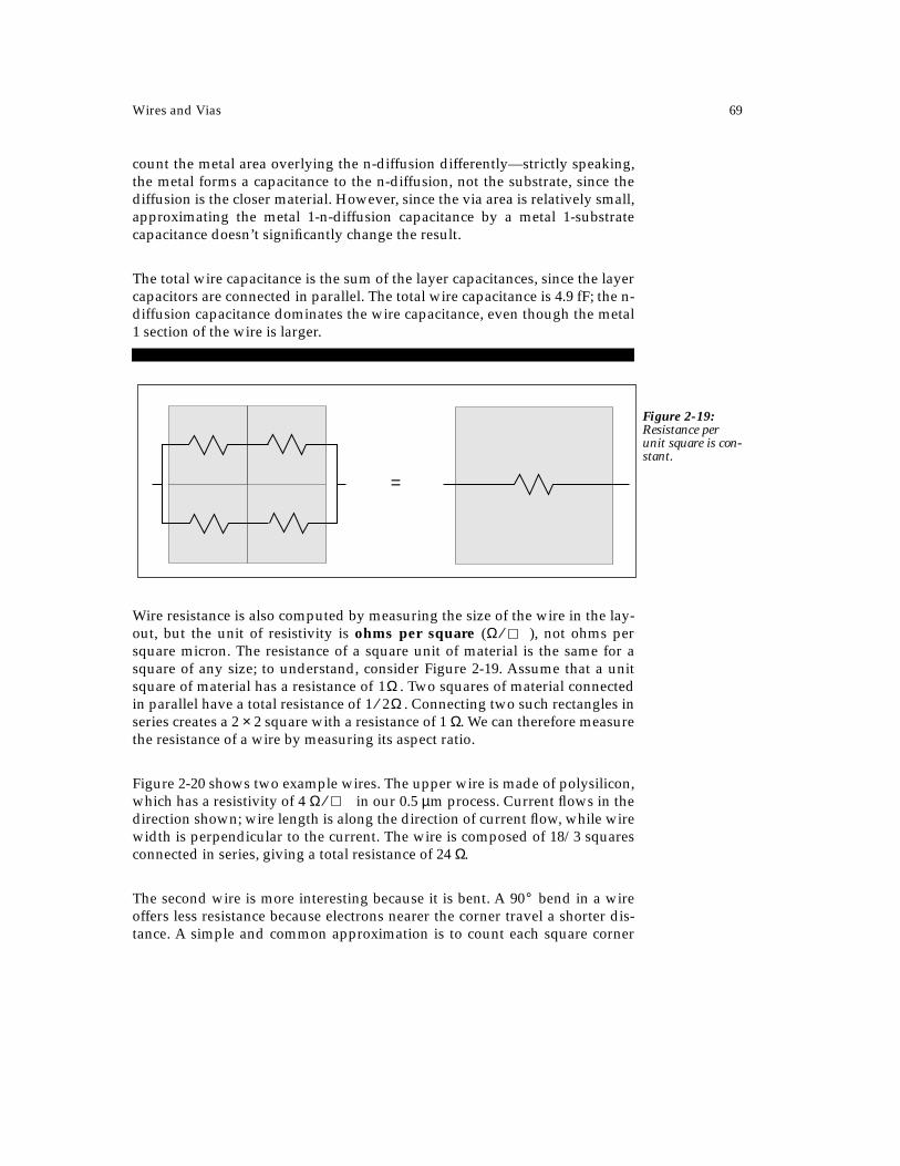
Wire resistance is also computed by measuring the size of the wire in the lay-out, but the unit of resistivity is ohms per square ( ), not ohms persquare micron. The resistance of a square unit of material is the same for asquare of any size; to understand, consider Figure 2-19. Assume that a unitsquare of material has a resistance of . Two squares of material connectedin parallel have a total resistance of . Connecting two such rectangles inseries creates a 2 × 2 square with a resistance of 1 Ω. We can therefore measurethe resistance of a wire by measuring its aspect ratio.
Figure 2-20 shows two example wires. The upper wire is made of polysilicon,which has a resistivity of 4 in our 0.5 µm process. Current flows in thedirection shown; wire length is along the direction of current flow, while wirewidth is perpendicular to the current. The wire is composed of 18/3 squaresconnected in series, giving a total resistance of 24 Ω.
The second wire is more interesting because it is bent. A bend in a wireoffers less resistance because electrons nearer the corner travel a shorter dis-tance. A simple and common approximation is to count each square corner
Figure 2-19: Resistance per unit square is con-stant.
=
Ω ⁄
1Ω1 2⁄ Ω
Ω ⁄
90°

70 Transistors and Layout
rectangle as 1/2 squares of resistance. The wire can be broken into threepieces: 9/3 = 3 squares, 1/2 squares, and 6/3 = 2 squares. P-diffusion resistiv-ity is approximately 2 , giving a total resistance of 11 Ω.
In our typical 0.5 µm process, an n-diffusion wire has a resistivity of approxi-mately 2 , with metal 1, metal 2, and metal 3 having resistivities ofabout 0.08, 0.07, and 0.03 , respectively. Note that p-diffusion wires inparticular have higher resistivity than polysilicon wires, and that metal wireshave low resistivities.
The source and drain regions of a transistor have significant capacitance andresistance. These parasitics are, for example, entered into a Spice simulationas device characteristics rather than as separate wire models. However, wemeasure the parasitics in the same way we would measure the parasitics onan isolated wire, measuring area and perimeter up to the gate-source/drainboundary.
Vias have added resistance because the cut between the layers is smaller thanthe wires it connects and because the materials interface introduces resis-tance. The resistance of the via is usually determined by the resistance of thematerials: a metal 1-metal 2 via has a typical resistance of less than 0.5 Ω whilea metal1-poly contact has a resistance of 2.5 Ω. We rarely worry about theexact via resistance in layout design; instead, we try to avoid introducingunnecessary vias in current paths for which low resistance is critical.
current 3λ
current
9λ
6λ
3λ
Figure 2-20: An example of resis-tance calculation.
Ω ⁄
Ω ⁄Ω ⁄

Design Rules 71
2.5 Design Rules
Layouts are built from three basic component types: transistors, wires, andvias. We have seen the structures of these components created during fabrica-tion. Now we will consider the design of the layouts which determine the cir-cuit that is fabricated. Design rules govern the layout of individualcomponents and the interactions—spacings and electrical connections—between those components. Design rules determine the low-level propertiesof chip designs: how small individual logic gates can be made; how small thewires connecting gates can be made, and therefore, the parasitic resistanceand capacitance which determine delay.
Design rules are determined by the conflicting demands of component pack-ing and chip yield. On the one hand, we want to make the components assmall as possible, to put as many functions as possible on-chip. On the otherhand, since the individual transistors and wires are about as small as thesmallest feature that our manufacturing process can produce, errors duringfabrication are inevitable: wires may short together or never connect, transis-tors may be faulty, etc. One common model for yield of a single type of struc-ture is a Gamma distribution [Mur93]:
. (EQ 2-27)
The total yield for the process is then the product of all the yield components:
. (EQ 2-28)
This formula suggests that low yield for even one of the process steps cancause serious final yield problems. But being too conservative about designrules leads to chips that are too large (which itself reduces yield) and too slowas well. We try to balance chip functionality and manufacturing yield by fol-lowing rules for layout design which tell us what layout constructs are likelyto cause the greatest problems during fabrication.
Yi1
1 Aβi+-------------------
α i
=
Y Yii 1=
n
∏=
72 Transistors and Layout
2.5.1 Fabrication Errors
The design rules for a particular process can be confusing unless you under-stand the motivation for the rules—the types of errors that are likely to occurwhile the chip is being manufactured. The design rules for a process are for-mulated to minimize the occurrence of common fabrication problems andbring the yield of correct chips to an acceptable level.
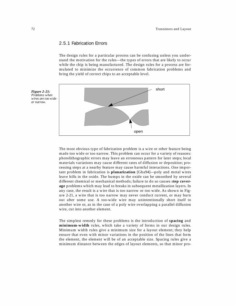
The most obvious type of fabrication problem is a wire or other feature beingmade too wide or too narrow. This problem can occur for a variety of reasons:photolithographic errors may leave an erroneous pattern for later steps; localmaterials variations may cause different rates of diffusion or deposition; pro-cessing steps at a nearby feature may cause harmful interactions. One impor-tant problem in fabrication is planarization [Gha94]—poly and metal wiresleave hills in the oxide. The bumps in the oxide can be smoothed by severaldifferent chemical or mechanical methods; failure to do so causes step cover-age problems which may lead to breaks in subsequent metallization layers. Inany case, the result is a wire that is too narrow or too wide. As shown in Fig-ure 2-21, a wire that is too narrow may never conduct current, or may burnout after some use. A too-wide wire may unintentionally short itself toanother wire or, as in the case of a poly wire overlapping a parallel diffusionwire, cut into another element.
The simplest remedy for these problems is the introduction of spacing andminimum-width rules, which take a variety of forms in our design rules.Minimum width rules give a minimum size for a layout element; they helpensure that even with minor variations in the position of the lines that formthe element, the element will be of an acceptable size. Spacing rules give aminimum distance between the edges of layout elements, so that minor pro-
Figure 2-21: Problems when wires are too wide or narrow.
short
open

Design Rules 73
cessing variations will not cause the element to overlap nearby layout ele-ments.
We also have a number of composition rules to ensure that components arewell-formed. Consider the transistor layout in Figure 2-22—the transistoraction itself takes place in the channel, at the intersection of the polysiliconand diffusion regions, but a valid transistor layout requires extensions of boththe poly and diffusion regions beyond the boundary. The poly extensionsensure that no strand of diffusion shorts together the source and drain. Thediffusion extensions ensure that adequate contact can be made to the sourceand drain.
Vias have construction rules as well: the material on both layers to be con-nected must extend beyond the SiO
2 cut itself; and the cut must be of a fixed
size. As shown in Figure 2-23, the overlap requirement simply ensures thatthe cut will completely connect the desired layout elements and not mistak-enly connect to the substrate or another wire. The key problem in via fabrica-tion, however, is making the cuts. A large chip may contain millions of vias,all of which must be opened properly for the chip to work. The acid etchingprocess which creates cuts must be very uniform—cuts may be neither toosmall and shallow nor too large. It isn’t hard to mount a bookcase in a wallwith an electric drill—it is easy to accurately size and position each hole
Figure 2-22: Potential problems in transistor fabri-cation.
diffusionshorts channel
Figure 2-23: Potential prob-lems in via fabrica-tion.
misaligned bloated

74 Transistors and Layout
required. Now imagine making those holes by covering the wall with acid atselected points, then wiping the wall clean after a few minutes, and youshould empathize with the problems of manufacturing vias on ICs. The cutmust also be filled with material without breaking as the material flows overthe edge of the cut. The size, shape, and spacing of via cuts are all strictly reg-ulated by modern fabrication processes to give maximum via yield.
2.5.2 Scalable Design Rules
Manufacturing processes are constantly being improved. The ability to makeever-smaller devices is the driving force behind Moore’s Law. But many char-acteristics of the fabrication process do not change as devices shrink—layoutsdo not have to be completely redesigned, simply shrunk in size. We can takebest advantage of process scaling by formulating our design rules to beexplicitly scalable.
We will scale our design rules by expressing them not in absolute physicaldistances, but in terms of λ, the size of the smallest feature in a layout. All fea-tures can be measured in integral multiples of λ. By choosing a value for λ weset all the dimensions in a scalable layout.
Scaling layouts makes sense because chips actually get faster as layoutsshrink. As a result, we don’t have to redesign our circuits for each new pro-cess to ensure that speed doesn’t go down as packing density goes up. If cir-cuits became slower with smaller transistors, then circuits and layouts wouldhave to be redesigned for each process.
Digital circuit designs scale because the capacitive loads that must be drivenby logic gates shrink faster than the currents supplied by the transistors in thecircuit [Den74]. To understand why, assume that all the basic physical param-eters of the chip are shrunk by a factor 1/x:
• lengths and widths: W → W/x, L → L/x;
• vertical dimensions such as oxide thicknesses: tox
→ tox
/x;
• doping concentrations: Nd → N
d/x;
• supply voltages: VDD
- VSS
→ (VDD
- VSS
)/x.
We now want to compute the values of scaled physical parameters, which wewill denote by variables with hat symbols. One result is that the transistor

Design Rules 75
transconductance scales: since [Mul77], . ( isthe carrier mobility and is the dielectric constant.) The threshold voltagescales with oxide thickness, so . Now compute the scaling of thesaturation drain current W/L:
(EQ 2-29)
The scaling of the gate capacitance is simple to compute: ,so . The total delay of the logic circuit depends on the capaci-tance to be charged, the current available, and the voltage through which thecapacitor must be charged; we will use as a measure of the speed of acircuit over scaling. The voltage through which the logic circuit swings isdetermined by the power supply, so the voltage scales as . When we plugin all our values,
. (EQ 2-30)
So, as the layout is scaled from λ to , the circuit is actually speededup by a factor x.
In practice, few processes are perfectly λ-scalable. As process designers learnmore, they inevitably improve some step in the process in a way that does notscale. High-performance designs generally require some modification whenmigrated to a smaller process as detailed timing properties change. However,the scalability of VLSI systems helps contain the required changes.
2.5.3 SCMOS Design Rules
Finally, we reach the SCMOS design rules themselves1. We will cast theserules in terms of λ. For the SCMOS rules, a 0.5 µm process, the nominal valuefor λ is 0.25 µm. However, fabrication lines often make minor adjustments tothe masks (bloating or shrinking) to adjust the final physical dimensions of
k' µeff εox( ) tox⁄= k'ˆ k'⁄ x= µeffεox
Vt Vt x⁄=
IdId---- k'ˆ
k'---
W L⁄W L⁄-------------
Vgs Vt–( )2
Vgs Vt–( )2-----------------------------=
x 1 x⁄1 x⁄----------
1x---
2=
1x---=
Cg εoxWL tox⁄=Cg Cg⁄ 1 x⁄=
CV I⁄
1 x⁄
CV I⁄CV I⁄--------------- 1
x---=
λ λ x⁄=
76 Transistors and Layout
the features. We will concentrate on the rules for the basic two-level metalprocess, with some discussion of the rules for metal 3, since the rules for thehigher levels of metal are not as well standardized as for the two-level metalprocess. At this writing, MOSIS provides up to four metal layers in some pro-cesses.
Design rules are generally specified as pictures illustrating basic situations,with notes to explain features not easily described graphically. While this pre-sentation may be difficult to relate to a real layout, practice will teach you toidentify potential design rule violations in a layout from the prototype situa-tions in the rules. Many layout editor programs, such as Magic [Ost84], havebuilt-in design-rule checkers which will identify design-rule violations on thescreen for you. Using such a program is a big help in learning the processdesign rules.
Figure 2-24 summarizes the design rules. Classifying the situations describedin these pictures as separation, minimum size, or composition will help youdistinguish and learn the rules. Many of these rules hold for any tub struc-ture: n-tub, p-tub, or twin-tub. The rules regarding tubs and tub ties necessar-ily depend on the tub structure, however.
The basic separation and minimum size rules are:
• metal 1 Minimum width is 3 λ, minimum separation is 3 λ.
• metal 2 Minimum width is 3 λ, minimum separation is 4 λ.
• polysilicon Minimum width is 2 λ, minimum poly–poly separationis 2 λ.
• p-, n-diffusion Minimum width is 3 λ, minimum separationbetween same-type diffusions is 3 λ, minimum p-diff–n-diff separa-tion is 10 λ.
• tubs Tubs must be at least 10 λ wide. The minimum distance from thetub edge to source/drain active area is 5 λ.
The basic construction rules are:
1. We will describe the most recent set of rules available to us. Since theserules change over time, it is always best to consult MOSIS(http://www.mosis.org) before starting a design that will be fabricatedusing the SCMOS rules.

Design Rules 77
poly
metal 1
metal 2
tub tie
p-type transistor
p diff
n diff
n-type
tub tie
n diff vias
transistors
2 λ
p tub
n tub
2 λ
10 λ
2 λ
3 λ
3 λ
3 λ
3 λ
3 λ
3 λ
3 λ
3 λ4 λ
Figure 2-24: A summary of the SCMOS design rules for two-level metal processes.

78 Transistors and Layout
• transistors The smallest transistor is of width 3 λ and length 2 λ; polyextends 2 λ beyond the active region and diffusion extends 3 λ. Theactive region must be at least 1 λ from a poly-metal via, 2 λ fromanother transistor, and 3 λ from a tub tie.
• vias Cuts are 2 λ × 2 λ; the material on both layers to be connectedextends 1 λ in all directions from the cut, making the total via size 4 λ× 4 λ. (MOSIS also suggests another via construction with 1.5 λ ofmaterial around the cut. This construction is safer but the fractionaldesign rule may cause problems with some design tools.) Availablevia types are:
• n/p-diffusion–poly;
• poly–metal 1;
• n/p-diffusion–metal 1;
• metal 1–metal 2;
If several vias are placed in a row, successive cuts must be at least 2 λ apart.Spacing to a via refers to the complete 4 λ × 4 λ object, while spacing to a viacut refers to the 2 × 2 λ cut.
• tub ties A p-tub tie is made of a 2 λ × 2 λ cut, a 4 λ × 4 λ metal ele-ment, and a 4 λ × 4 λ p+ diffusion. An n-tub tie is made with an n+ dif-fusion replacing the p+ diffusion. A tub tie must be at least 2 λ from adiffusion contact.
It is important to remember that different rules have different dependencieson electrical connectivity. Spacing rules for wires, for example, depend onwhether the wires are on the same electrical node. Two wire segments on thesame electrical node may touch. However, two via cuts must be at least 2 λapart even if they are on the same electrical net. Similarly, two active regionsmust always be 2 λ apart, even if they are parallel transistors.
The rules for metal 3 are:
• Minimum metal 3 width is 6 λ, minimum separation is 4 λ.
• Available via from metal 3 is to metal 2. Connections from metal 3 toother layers must be made by first connecting to metal 2.
There are some specialized rules that do not fit into the separation/minimumsize/composition categorization.

Design Rules 79
• A cut to polysilicon must be at least 3 λ from other polysilicon.
• Polysilicon cuts and diffusion cuts must be at least 2 λ apart.
• A cut must be at least 2 λ from a transistor active region.
• A diffusion contact must be at least 4 λ away from other diffusion.
• A metal 2 via must not be directly over polysilicon.
One final special rule is to avoid generating small negative features. Con-sider the layout of Figure 2-25: the two edges of the notch are 1 λ apart, butboth sides of the notch are on the same electrical node. The two edges are notin danger of causing an inadvertent short due to a fabrication error, but thenotch itself can cause processing errors. Some processing steps are, for conve-nience, done on the negative of the mask given, as shown in the figure. Thenotch in the positive mask forms a 1λ wide protrusion on the negative mask.Such a small feature in the photoresist can break off during processing, floataround the chip, and land elsewhere, causing an unwanted piece of material.We can minimize the chances of stray photoresist causing problems byrequiring all negative features to be at least 2 λ in size.
2.5.4 Typical Process Parameters
Typical values of process parameters for a 0.5 µm fabrication process aregiven in Table 2-4. We use the term typical loosely here; these are estimatedvalues which do not reflect a particular manufacturing process and the actualparameter values can vary widely. You should always request process param-eters from your vendor when designing a circuit that you intend to fabricate.
Figure 2-25: A negative mask fea-ture.
negative feature

80 Transistors and Layout
Table 2-4 Typical parameters for our 0.5 µm process.
n-type transconductance k’np-type transconductance k’pn-type threshold voltage Vtn
p-type threshold voltage Vtp
gate capacitance Cg
n-diffusion bottomwall capacitance Cndiff,bot
n-diffusion sidewall capacitance Cndiff,side
p-diffusion bottomwall capacitance Cpdiff,bot
p-diffusion sidewall capacitance Cpdiff,side
n-type source/drain resistivity Rndiff
p-type source/drain resistivity Rpdiff
poly-substrate plate capacitance Cpoly,plate
poly-substrate fringe capacitance Cpoly,fringe
poly resistivity Rpoly
metal 1-substrate plate capacitance Cmetal1,plate
metal 1-substrate fringe capacitance Cmetal1,fringe
metal 2-substrate capacitance Cmetal2,plate
metal 2-substrate fringe capacitance Cmetal2,fringe
metal 3-substrate capacitance Cmetal3,plate
metal 3-substrate fringe capacitance Cmetal3,fringe
metal 1 resistivity Rmetal1
metal 2 resistivity Rmetal2
metal 3 resistivity Rmetal3
metal current limit Im,max
73µA V2⁄
21– µA V2⁄
0.7V
0.8V–
0.9fF µm2⁄
0.6fF µm2⁄
0.2fF µm⁄
0.9fF µm2⁄
0.3fF µm⁄
2Ω ⁄
2Ω ⁄
0.09fF µm2⁄
0.04fF µm⁄
4Ω ⁄
0.04fF µm2⁄
0.09fF µm⁄0.02fF µm2⁄0.06fF µm⁄0.009fF µm2⁄0.02fF µm⁄0.08Ω ⁄
0.07Ω ⁄
0.03Ω ⁄
1.5mA µm⁄

Layout Design and Tools 81
2.6 Layout Design and Tools
2.6.1 Layouts for Circuits
We ultimately want to design layouts for circuits. Layout design requires notonly a knowledge of the components and rules of layout, but also strategiesfor designing layouts which fit together with other circuits and which havegood electrical properties.
Since layouts have more physical structure than schematics, we need to aug-ment our terminology. Chapter 1 introduced the term net to describe a set ofelectrical connections; a net corresponds to a variable in the voltage equa-tions, but since it may connect many pins, it is hard to draw. A wire is a set ofpoint-to-point connections; as shown in Figure 2-26, a wire may containmany branches. The straight sections are called wire segments.
The starting point for layout is a circuit schematic. The schematic symbolsfor n- and p-type transistors are shown in Figure 2-27. The schematic showsall electrical connections between transistors (except for tub ties, which areoften omitted to simplify the diagram); it must also be annotated with theW/L of each transistor. We will discuss the design of logic circuits from tran-sistors in detail in Chapter 3. At this point, we will treat the circuit schematic
Figure 2-26: Wires and wire segments.
wiresegments
n-type p-type
Figure 2-27: Schematic sym-bols for transis-tors.

82 Transistors and Layout
as a specification for which we must implement the transistors and connec-tions in layout. (Most professional layout designers, in fact, have no trainingin electrical engineering and treat layout design strictly as an artwork designproblem.) The next example walks through the design of an inverter’s layout.
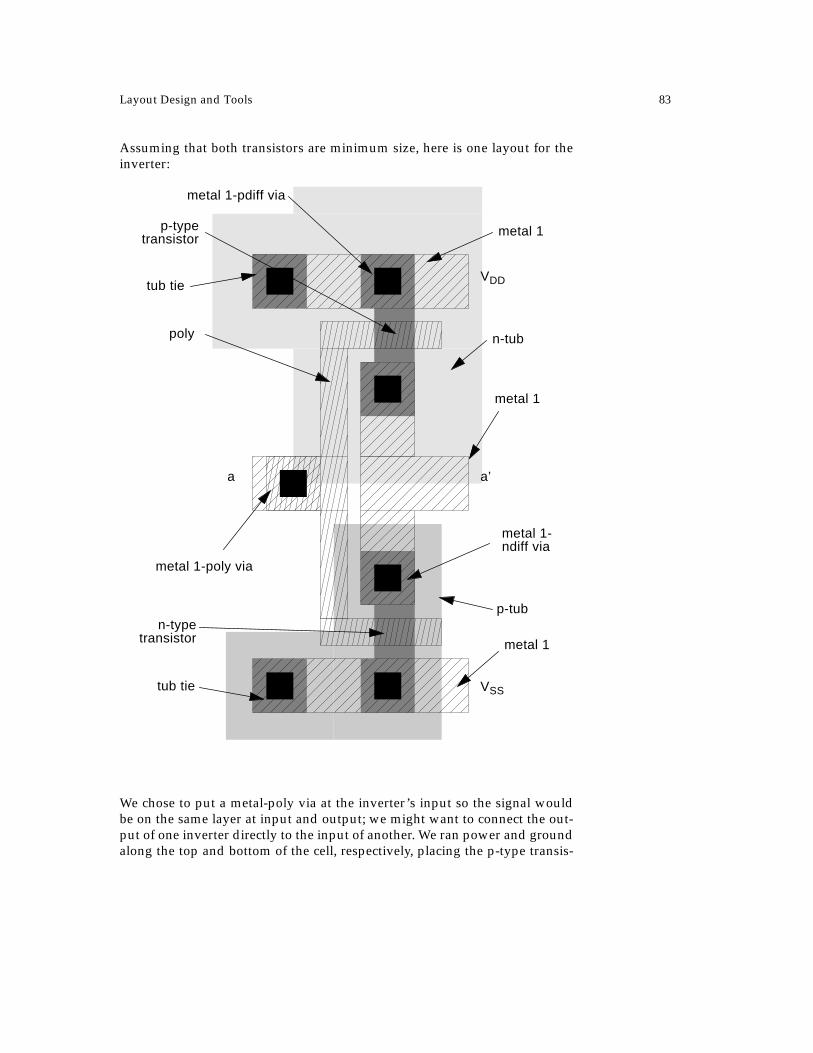
Example 2-5: Design of an inverter layout
The inverter circuit is simple (+ is VDD and the triangle is VSS):
In thinking about how the layout will look, a few problems become clear.First, we cannot directly connect the p-type and n-type transistors with pdiffand ndiff wires. We must use vias to go from ndiff to metal and then to pdiff.Second, the in signal is naturally in polysilicon, but the out signal is naturallyin metal, since we must use a metal strap to connect the transistors’ sourceand drain. Third, we must use metal for the power and ground connections.We probably want to place several layouts side-by-side, so we will run thepower/ground signals from left to right across the layout.
outin
+
Layout Design and Tools 83
Assuming that both transistors are minimum size, here is one layout for theinverter:
We chose to put a metal-poly via at the inverter’s input so the signal wouldbe on the same layer at input and output; we might want to connect the out-put of one inverter directly to the input of another. We ran power and groundalong the top and bottom of the cell, respectively, placing the p-type transis-
metal 1
VDD
VSS
a’a
p-typetransistor
poly
n-typetransistor
tub tie
metal 1
metal 1
metal 1-pdiff via
p-tub
metal 1-poly via
n-tub
tub tie
metal 1-ndiff via

84 Transistors and Layout
tor in the top half and the n-type in the bottom half. Larger layouts with manytransistors follow this basic convention: p-type on the top, n-type on the bot-tom. The large tub spacing required between p-type and n-type devicesmakes it difficult to mix them more imaginatively. We also included a tub tiefor both the n-tub and p-tub.
2.6.2 Stick Diagrams
We must design a complete layout at some point, but designing a complexsystem directly in terms of rectangles can be overwhelming. We need anabstraction between the traditional transistor schematic and the full layout tohelp us organize the layout design. A stick diagram is a cartoon of a chip lay-out. Figure 2-28 shows a stick diagram for an inverter. The stick diagram rep-resents the rectangles with lines which represent wires and componentsymbols. While the stick diagram does not represent all the details of a layout,it makes some relationships much clearer and it is simpler to draw.
Layouts are constructed from rectangles, but stick diagrams are built fromcartoon symbols for components and wires. The symbols for wires used onvarious layers are shown in Figure 2-29. You probably want to draw yourown stick diagrams in color: red for poly, green for n-diffusion, yellow for p-diffusion, and shades of blue for metal are typical colors. A few simple rulesfor constructing wires from straight-line segments ensure that the stick dia-gram corresponds to a feasible layout. First, wires cannot be drawn at arbi-trary angles—only horizontal and vertical wire segments are allowed.Second, two wire segments on the same layer which cross are electrically con-nected. Vias to connect wires that do not normally interact are drawn as black
Figure 2-28: A stick diagram for an inverter.
outin
VDD
VSS

Layout Design and Tools 85
dots. Figure 2-30 shows the stick figures for transistors—each type of transis-tor is represented as poly and diffusion crossings, much as in the layout.
The complete rules which govern how wires on different layers interact areshown in Table 2-5; they tell whether two wires on given layers are allowed tocross and, if so, the electrical properties of the new construct. This table isderived from the manufacturing design rules.
Stick diagrams are not exact models of layouts. Most of the differences arecaused by the use of zero-width lines and zero-area transistors in stick dia-grams. When you draw a layout using a stick diagram as a guide, you mayfind it necessary to move transistors and vias and to reroute wires. Area and
metal2
metal1
poly
ndiff
pdiff
metal3 Figure 2-29: Stick diagram symbols for wires.
n-type p-type
electricallyconnected
via
Figure 2-30: Symbols for com-ponents in stick diagrams.
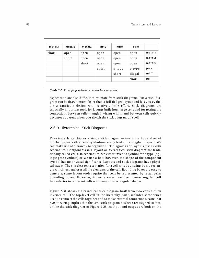
86 Transistors and Layout
aspect ratio are also difficult to estimate from stick diagrams. But a stick dia-gram can be drawn much faster than a full-fledged layout and lets you evalu-ate a candidate design with relatively little effort. Stick diagrams areespecially important tools for layouts built from large cells and for testing theconnections between cells—tangled wiring within and between cells quicklybecomes apparent when you sketch the stick diagram of a cell.
2.6.3 Hierarchical Stick Diagrams
Drawing a large chip as a single stick diagram—covering a huge sheet ofbutcher paper with arcane symbols—usually leads to a spaghetti layout. Wecan make use of hierarchy to organize stick diagrams and layouts just as withschematics. Components in a layout or hierarchical stick diagram are tradi-tionally called cells. In schematics, we either invent a symbol for a type (e.g.,logic gate symbols) or we use a box; however, the shape of the componentsymbol has no physical significance. Layouts and stick diagrams have physi-cal extent. The simplest representation for a cell is its bounding box: a rectan-gle which just encloses all the elements of the cell. Bounding boxes are easy togenerate; some layout tools require that cells be represented by rectangularbounding boxes. However, in some cases, we use non-rectangular cellboundaries to represent cells with very non-rectangular shapes.
Figure 2-31 shows a hierarchical stick diagram built from two copies of aninverter cell. The top-level cell in the hierarchy, pair1, includes some wiresused to connect the cells together and to make external connections. Note thatpair1’s wiring implies that the inv1 stick diagram has been redesigned so that,unlike the stick diagram of Figure 2-28, its input and output are both on the
Table 2-5 Rules for possible interactions between layers.
metal3 metal2 metal1 poly ndiff pdiff
short open open open open open metal3
short open open open open metal2
short open open open metal1
short n-type p-type poly
short illegal ndiff
short pdiff
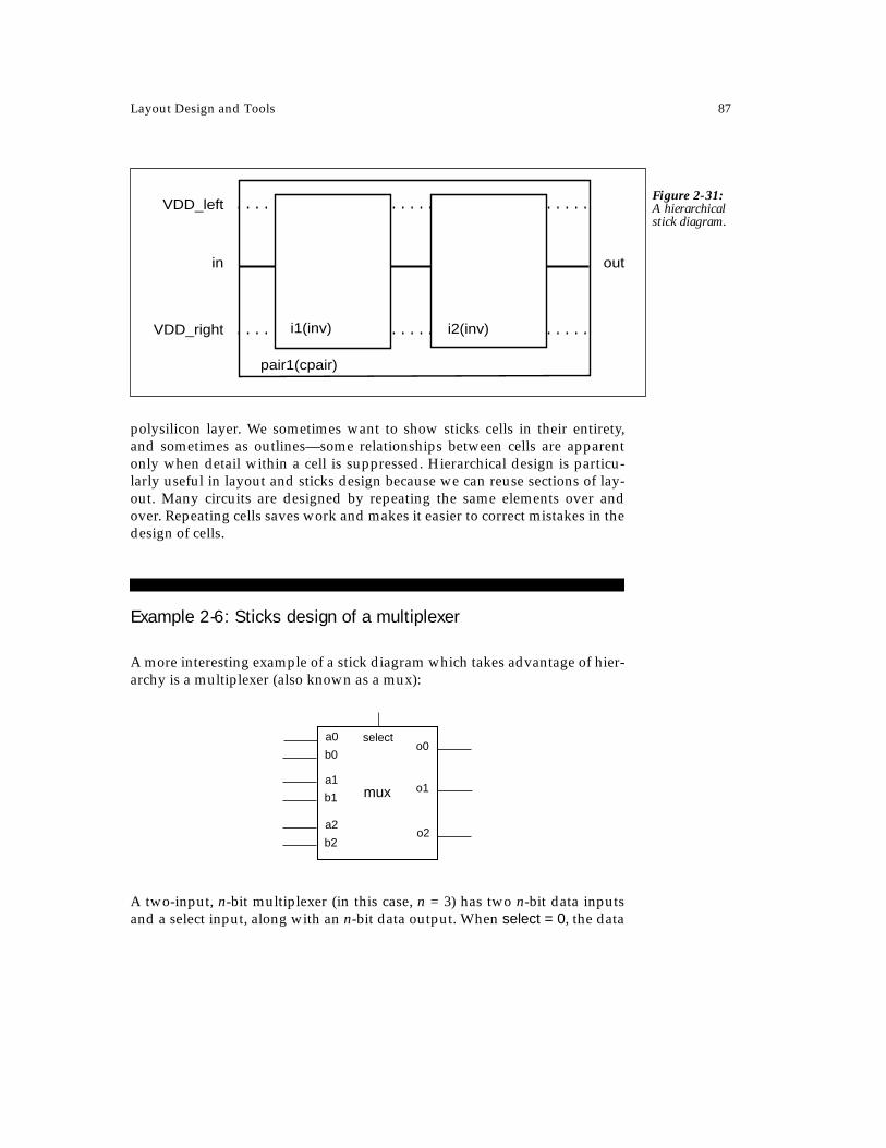
Layout Design and Tools 87
polysilicon layer. We sometimes want to show sticks cells in their entirety,and sometimes as outlines—some relationships between cells are apparentonly when detail within a cell is suppressed. Hierarchical design is particu-larly useful in layout and sticks design because we can reuse sections of lay-out. Many circuits are designed by repeating the same elements over andover. Repeating cells saves work and makes it easier to correct mistakes in thedesign of cells.
Example 2-6: Sticks design of a multiplexer
A more interesting example of a stick diagram which takes advantage of hier-archy is a multiplexer (also known as a mux):
A two-input, n-bit multiplexer (in this case, n = 3) has two n-bit data inputsand a select input, along with an n-bit data output. When select = 0, the data
i1(inv) i2(inv)
out
VDD_left
in
VDD_right
pair1(cpair)
Figure 2-31: A hierarchical stick diagram.
a0
b0
a1
b1
a2
b2
o0
o1
o2
mux
select
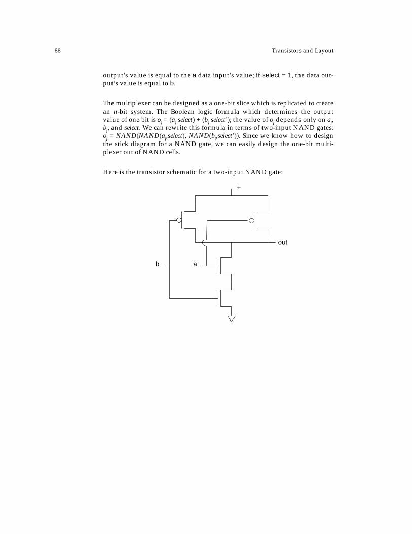
88 Transistors and Layout
output’s value is equal to the a data input’s value; if select = 1, the data out-put’s value is equal to b.
The multiplexer can be designed as a one-bit slice which is replicated to createan n-bit system. The Boolean logic formula which determines the outputvalue of one bit is o
i = (a
i select) + (b
i select’); the value of o
i depends only on a
i,
bi, and select. We can rewrite this formula in terms of two-input NAND gates:
oi = NAND(NAND(a
i,select), NAND(b
i,select’)). Since we know how to design
the stick diagram for a NAND gate, we can easily design the one-bit multi-plexer out of NAND cells.
Here is the transistor schematic for a two-input NAND gate:
+
ab
out

Layout Design and Tools 89
And here is a stick diagram for the two-input NAND:
We can use the NAND cell to build a one-bit multiplexer cell:
In this case we’ve drawn the hierarchical stick diagram using boundingboxes; to design the complete layout we would have to look into the cells.The connections designed between NAND cells were designed to avoid cre-ating unwanted shorts with wires inside the NANDs; to be completely surethe intercell wires do not create problems, you must expand the view of thebit slice to include the internals of the NAND cells. However, making an ini-tial wiring design using the NANDs as boxes, remembering the details oftheir internals as you work, makes it easier to see the relationships betweenwires that go between the cells.
out
a
VDD
VSS
b
a
b
out
VDD
VSS
a
b
out
VDD
VSS
a
b
out
VDD
VSS
select'
VDD
VSS
aibi
oi
n1(NAND) n2(NAND) n3(NAND)
select
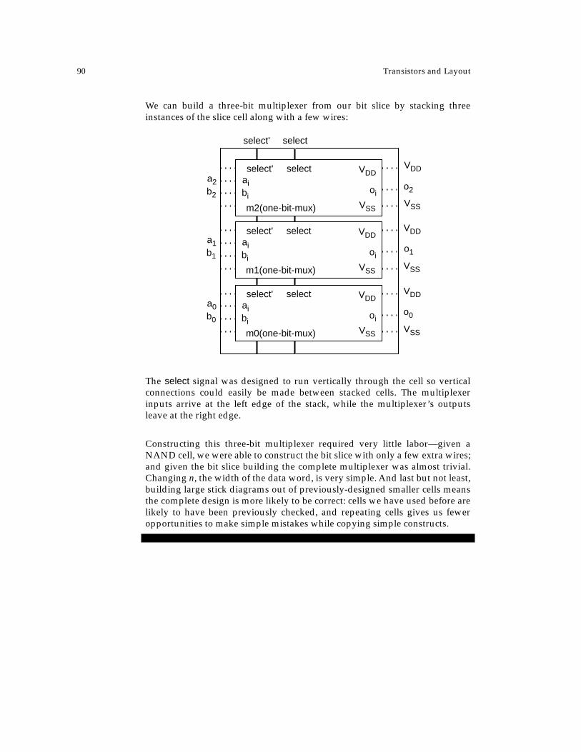
90 Transistors and Layout
We can build a three-bit multiplexer from our bit slice by stacking threeinstances of the slice cell along with a few wires:
The select signal was designed to run vertically through the cell so verticalconnections could easily be made between stacked cells. The multiplexerinputs arrive at the left edge of the stack, while the multiplexer’s outputsleave at the right edge.
Constructing this three-bit multiplexer required very little labor—given aNAND cell, we were able to construct the bit slice with only a few extra wires;and given the bit slice building the complete multiplexer was almost trivial.Changing n, the width of the data word, is very simple. And last but not least,building large stick diagrams out of previously-designed smaller cells meansthe complete design is more likely to be correct: cells we have used before arelikely to have been previously checked, and repeating cells gives us feweropportunities to make simple mistakes while copying simple constructs.
m2(one-bit-mux)
select' VDD
VSS
aibi
oi
m1(one-bit-mux)
select' VDD
VSS
aibi
oi
m0(one-bit-mux)
select' VDD
VSS
aibi
oi
a2b2
o2
select'
a1b1
a0b0
o1
o0
VDD
VSS
VDD
VSS
VDD
VSS
select
select
select
select
Layout Design and Tools 91
2.6.4 Layout Design and Analysis Tools
A variety of CAD tools help us design and verify layouts. The most impor-tant tools are layout editors, design rule checkers, and circuit extractors.
A layout editor is an interactive graphic program that lets you create anddelete layout elements. Most layout editors work on hierarchical layouts,organizing the layout into cells which may include both primitive layout ele-ments and other cells. Some layout editing programs, such as Magic, work onsymbolic layouts, which include somewhat more detail than do stick dia-grams but are still more abstract than pure layouts. A via, for example, maybe represented as a single rectangle while you edit the symbolic layout; whena final physical layout is requested, the symbolic via is fleshed out into all therectangles required for your process. Symbolic layout has several advantages:the layout is easier to specify because it is composed of fewer elements; thelayout editor ensures that the layouts for the symbolic elements are properlyconstructed; and the same symbolic layout can be used to generate severalvariations, such as n-tub, p-tub, and twin-tub versions of a symbolic design.
A design rule checker (often called a DRC program), as the name implies,looks for design rule violations in the layout. It checks for minimum spacingand minimum size and ensures that combinations of layers form legal com-ponents. The results of the DRC are usually shown as highlights. on top of thelayout. Some layout editors, including Magic, provide on-line design rulechecking. Design rule checking algorithms are briefly described in Chapter10.
Circuit extraction is an extension of design rule checking and uses similaralgorithms. A design rule checker must identify transistors and vias to ensureproper checks—otherwise, it might highlight a transistor as a poly-diffusionspacing error. A circuit extractor performs a complete job of component andwire extraction. It produces a net list which lists the transistors in the layoutand the electrical nets which connect their terminals. Vias do not appear inthe net list—a via simply merges two nets into a single larger net. The circuitextractor usually measures parasitic resistance and capacitance on the wiresand annotates the net list with those parasitic values. The next exampledescribes how we can extract a circuit from a layout.

92 Transistors and Layout
Example 2-7: Circuit extraction
We will extract the circuit by successively identifying, then deleting compo-nents. After all component types have been extracted, only the wires willremain.
Identifying components from the layout requires manipulating masks singlyand in combination. Grow and shrink are two important operations:
The grow operation increases the extent of each polygon in the mask by afixed amount in every direction; the shrink operation does the converse. Wewill also need to form Boolean combinations of masks: the NOT of a maskcovers all the area not covered by the mask itself; the AND of two masks cov-ers only the area under both masks; and the OR includes the area covered byeither mask. Boolean and grow/shrink operations generate new masks.
When we extract the circuit, we will assume the layout has no design-ruleerrors; we can always DRC the layout before extraction. We can identify allthe transistors in the layout very easily: the n-type transistors’ active areas areexactly the AND of the poly and the n-diff masks, with analogous definitionfor the p-type transistors. After identifying the transistors, we can removethem from the layout of the active-area mask, which leaves the gate, source,and drain connections hanging. We will mark and remember the locations ofthe transistors’ terminals for the final step of extraction.
Identifying vias requires a little more effort. To identify poly-metal1 vias, wefirst grow the cut mask by 2λ, then we form the AND of the grown-cut, metal,and poly masks. The result is one 4λ-by-4λ square for each poly-metal1 via.After identifying all the vias, we remove them while marking their place. We
grow
Layout Design and Tools 93
can identify tub ties, but we won’t need them for the later stages of analysis,since they don’t make new electrical connections.
At this point, only the wires are left in the layout. A polygon on one layerforms an electrically connected region. However, we’re not quite done,because connections may have been made by vias or by wires through tran-sistors. To take account of all connections, we must first identify where eachwire touches a connection point to a via or transistor. We then form the transi-tive closure of all the connection points: if one wire connects points A and B,and another wire connects B and C, then A, B, and C are all electrically con-nected.
Once we have traced through all the connections, we have a basic circuitdescription. We have not yet taken parasitics into account. To do so, we mustcount parasitics for each wire, via, and transistor, then mark each electricalnode appropriately. However, for simple functional analysis, extracting para-sitics may not be necessary. Here is a fragment of an extracted circuit writtenin Magic’s ext format:
The exact format of this file isn’t important, but a few details should helpmake this information less forbidding. A node record defines an electricalnode in the circuit—explicit declaration of the nodes simplifies the programwhich reads the file. The record gives total resistance and capacitance for thenode, an x, y position which can be used to identify the node in the layout,and area and perimeter information for resistance extraction. A cap recordgives two nodes and the capacitance between them. A fet record describes thetype of transistor, the corners of its channel, and the electrical nodes to whichthe source, drain, and gate are connected.
node “6_38_29#” 122 55 19 -14 green 0 0 0 0 54 34 0 0 92 62 0 0 0 0 0 0node “6_50_15#” 120 10 25 -7 green 0 0 0 0 12 16 0 0 0 0 0 0 0 0 0 0node “6_50_7#” 521 92 25 -3 green 0 0 60 44 30 22 0 0 80 64 0 0 0 0 0 0node “6_36_19#” 825 12 18 -9 p 110 114 0 0 0 0 0 0 0 0 0 0 0 0 0 0node “6_36_11#” 690 9 18 -5 p 92 96 0 0 0 0 0 0 0 0 0 0 0 0 0 0node “6_40_40#” 559 83 20 20 brown 0 0 80 54 0 0 0 0 68 58 0 0 0 0 0 0cap “6_36_19#” “6_50_7#” 1fet nfet 25 -9 26 -8 12 16 “GND!” “6_36_19#” 4 0 “6_38_29#” 6 0 “6_50_15#” 6 0fet nfet 25 -5 26 -4 12 16 “GND!” “6_36_11#” 4 0 “6_50_15#” 6 0 “6_50_7#” 6 0fet pfet 39 17 40 18 12 16 “Vdd!” “6_36_19#” 4 0 “6_50_7#” 6 0 “6_40_40#” 6 0fet pfet 25 17 26 18 12 16 “Vdd!” “6_36_11#” 4 0 “6_50_7#” 6 0 “6_40_40#” 6 0

94 Transistors and Layout
The simplest extraction algorithm works on a layout without cells—this isoften called flat circuit extraction because the component hierarchy is flat-tened to a single level before extraction. However, a flattened layout is verylarge: a layout built of one 100-rectangle cell repeated 100 times will have 100rectangles plus 100 (small) cell records; the same layout flattened to a singlecell will have 10,000 rectangles. That added size claims penalties in disk stor-age, main memory, and CPU time.
Hierarchical circuit extraction extracts circuits directly on the hierarchicallayout description. Dealing with cell hierarchies requires more sophisticatedalgorithms which are beyond our scope. Hierarchical extraction may alsorequire design restrictions, such as eliminating overlaps between cells. How-ever, one problem which must be solved illustrates the kinds of problemsintroduced by component hierarchies.
Consider the example of Figure 2-32. Each cell has its own net list. The netlists of leaf cells make sense on their own, but A’s net list is written in terms ofits components. We often want to generate a flattened net list—flattening thenet list after extraction makes sense because the net list is much smaller thanthe layout. To create the flattened net list, we must make correspondencesbetween nets in the cells and nets in the top-level component. Once again, weuse transitive closure: if net o in cell B is connected to n2 in A, which in turn isconnected to net a in C, then B.o, A.n2, and C.a are all connected. Flatteningalgorithms can be very annoying if they choose the wrong names for com-bined elements. In this case, n2, the top-level component’s name for the net, isprobably the name most recognizable to the designer.
i oa
bo
n1n2
i
x
A
B C
B C
Figure 2-32: Tracing nets for hierarchical cir-cuit extraction.

Layout Design and Tools 95
An extracted layout has two important uses. First, the extracted circuit can besimulated and the results compared to the specified circuit design. Seriouslayout errors, such as a missing transistor or wire, should show up as a differ-ence in the specified and extracted circuits. Second, extracted parasitics canbe used to calculate actual delays. Circuit performance may have been esti-mated using standard parasitic values or parasitics may have been ignoredentirely, but long wires can slow down logic gates. Comparing the actual per-formance of the extracted layout to the predicted performance tells youwhether the logic and circuits need to be modified and, if so, where criticaldelay problems exist.
2.6.5 Automatic Layout
Hierarchical stick diagrams are a good way to design large custom cells. Butyou will probably design large cells from scratch infrequently. You are muchmore likely to use layouts generated by one of two automated methods: cellgenerators (also known macrocell generators), which create optimized lay-outs for specialized functions such as ALUs; or standard cell placement androuting, which use algorithms to build layouts from gate-level cells.
A cell generator is a parameterized layout—it is a program written by a per-son to generate the layout for a particular cell or a families of cells. The gener-ator program is usually written textually, though some graphical layouteditors provide commands to create parameterized layouts. If the generatorcreates only one layout, it may as well have been created with a graphical lay-out editor. But designers often want to create variations on a basic cell: chang-ing the sizes of transistors, choosing the number of busses which run througha cell, perhaps adding simple logic functions. Specialized functions likeALUs, register files, and RAMs often require careful layout and circuit designto operate at high speed. Generator languages let skilled designers createparameterized layouts for such cells which can be used by chip designerswhose expertise is in system design, not circuit and layout design.
Figure 2-33 shows a fragment of a layout generator written in the CLL lan-guage [Sax83]. The wire command works like a pen—it lays down material ona layer as it moves from point to point. Movement may be specified by abso-lute coordinate or by relative movement; a layer switch instantiates a via atthe point of the switch. This small example doesn’t show how to build layoutprocedures, which can take parameters much like procedures in program-ming languages. Parameters passed in at run time can control whether layoutelements are placed at all and where they are placed.
96 Transistors and Layout
Place-and-route programs take a very different approach to layout synthesis:they break the problem into placing components on the plane, then routingwires to make the necessary connections. Placement and routing algorithmsmay not be able to match the quality of hand-designed layouts for some spe-cialized functions, but they often do better than people on large random logicblocks because they have greater patience to search through large, unstruc-tured problems to find good solutions.
The most common placement-and-routing systems use standard cells, whichare logic gates, latches, flip-flops, or occasionally slightly larger functions likefull adders. Figure 2-34 shows the architecture of a standard cell layout: thecomponent cells, which are of standard height but of varying width, arearranged in rows; wires are run in routing channels between the cell rows,along the sides, and occasionally through feedthroughs (spaces left open forwires in the component cells). The layout is designed in two stages: compo-nents are placed using approximations to estimate the amount of wirerequired to make the connections; then the wires are routed. We will discuss
#define diff1 0,6#define via1 11,6#define poly1 5,12#define poly2 15,1/* wire starts in diffusion, goes to metal */wire ndiff diff1 via1 metal1 r 15 /* go right 15 */;/* poly wire*/wire poly poly1 d 4 /* go down 4 */ poly2;
generator program
generated layout
poly1
poly2
diffl via1
Figure 2-33: A layout generation program.

Layout Design and Tools 97
standard cell layout synthesis in more detail in Chapter 6. Figure 2-35 showsa small standard cell layout generated by the wolfe program [San84, Sec85].
cells
routing area
rout
ing
area
Figure 2-34: Architecture of a standard cell lay-out.
Figure 2-35: An example of stan-dard cell layout.

98 Transistors and Layout
2.7 References
As mentioned in the last chapter, Dennard et al. [Den74] first explained whyshrinking IC line widths led to higher performance as well as smaller chips.That observation led to the development of scalable design rules, which werefirst introduced by Mead and Conway [Mea80]. The specifications for theMOSIS SCMOS process were derived from MOSIS data. Complete documen-tation on the SCMOS rules is available on the World Wide Web athttp://www.isi.edu/mosis or by sending electronic mail to [email protected]. TheMOSIS SCMOS rules do occasionally change, so it is always best to consultMOSIS for the latest design rules before starting a design.

Problems 99
2.8 Problems
Use process parameters from Table 2-4 as required.
2-1. Draw the cross-section of the inverter shown below along a cut throughthe middle of the p-type and n-type transistors.
2-2. Assuming that Vgs = 3.3V, compute the drain current through n-typetransistors of these sizes at Vds values of 1V, 2V, 3.3V, and 5V:
a) W/L = 5/2.b) W/L = 8/2.c) W/L =12/2.d) W/L = 25/2.
2-3. Using the parameter values given in Example 2-2:
a) How much would you have to change the gate oxide thickness toreduce the threshold voltage by 0.1 V?
cut

100 Transistors and Layout
b) How much would you have to change the doping NA to reducethe threshold voltage by 0.1 V?
2-4. Plot Id vs. Vgs at Vds = 5V for two values of the channel length modulationparameter: λ = 0 and λ = 0.03.
2-5. Evaluate the effects of leakage currents:
a) First, compute the gate capacitance of a minimum-size transistor(ignoring source/drain overlap capacitances).b) Assuming that Il0 = 0.1 nA, how long will it take leakage currentsto drain half the charge of that gate capacitance, assuming that itstarts at 5 V?c) How long will it take for leakage currents to drain the capacitorassuming it starts at 3.3 V?
2-6. Justify each of these design rules:
a) 2λ poly-poly spacing;b) no required poly-metal spacing;c) 1λ of diffusion and metal surrounding cut;d) 2λ overhang of poly at transistor gate.
2-7. Explain:
a) Why is ndiff-to-pdiff spacing so large?b) Why is metal-metal spacing larger than poly-poly spacing?c) Why is metal2-metal2 spacing larger than metal1-metal1 spacing?
2-8. What distinguishes a tub tie from an ndiff-metal1 via?
2-9. Design the layout for an ndiff wire connected to a pdiff wire.
2-10. Compute the resistance and capacitance for each polysilicon wire below:
a)
b)
2λ
15λ

Problems 101
2-11. Compute the parasitic resistance and capacitance of the source/drainregion of transistors of the types and sizes given below, assuming that thesesource drain-regions have the required 2 λ overhang past the gate:
a) p-type; W/L = 3/2;b) n-type, W/L = 4/2;c) p-type; W/L = 6/2;d) n-type; W/L = 12/2.
2-12. Recompute the parasitic resistances and capacitances of the transistorsof Question 2-11. Assume in this case that the source/drain regions have therequired overhang but also include as many diffusion/metal 1 vias as will fitin the given gate width. Measure the total resistance including the via resis-tance.
2-13. Measure the parasitic resistance and capacitance on the input to theinverter shown on the next page. The transistors have W/L = 3 λ / 2 λ andthe VDD and VSS lines are each 4 λ wide. Give the total resistance and capaci-
2λ
2λ
15λ
4λ

102 Transistors and Layout
tance of all the material connected to the inverter’s input, showing how youbroke the layout elements into sections for measurement.
2-14. Reverse-engineer the layout shown on the next page. Draw:
a) a stick diagram corresponding to the layout;b) a transistor schematic.

Problems 103
Label inputs and outputs in your drawings in accordance with the labels inthe layout.
2-15. Design a layout for the circuit fragment below in two stages:
a) a stick diagram;b) the complete layout.
2-16. Design two different stick diagrams for the inverter circuit of Example2-5. Your only constraint is that both VDD and VSS must be available on twoopposite sides of the cell.
2-17. Expand the stick diagram for the one-bit-mux cell of Example 2-6 toinclude the wires in the NAND cells.
2-18. Redesign the three-bit multiplexer of Example 2-6 so that adjacent one-bit-mux cells share VDD and VSS lines. You can overlap cells to force sharingof wires.
104 Transistors and Layout
2-19. Design two different stick diagrams for this circuit, such that both VDDand VSS are available on two opposite sides of the cell:
2-20. Design a layout for the circuit shown below in two stages: first draw astick diagram, then design the complete layout. Assume that all transistorsare 3 λ / 2 λ. The power supply lines should run through the cell in metal 1,available on opposite sides of the cell.
2-21. Design a stick diagram for the circuit shown below, assuming that tran-sistor sizes have W/L = 3 λ / 2 λ except as indicated. The cell should bedesigned to be area-efficient and to be horizontally tilable—you should be
+
ab
out
+
i1
i2
out
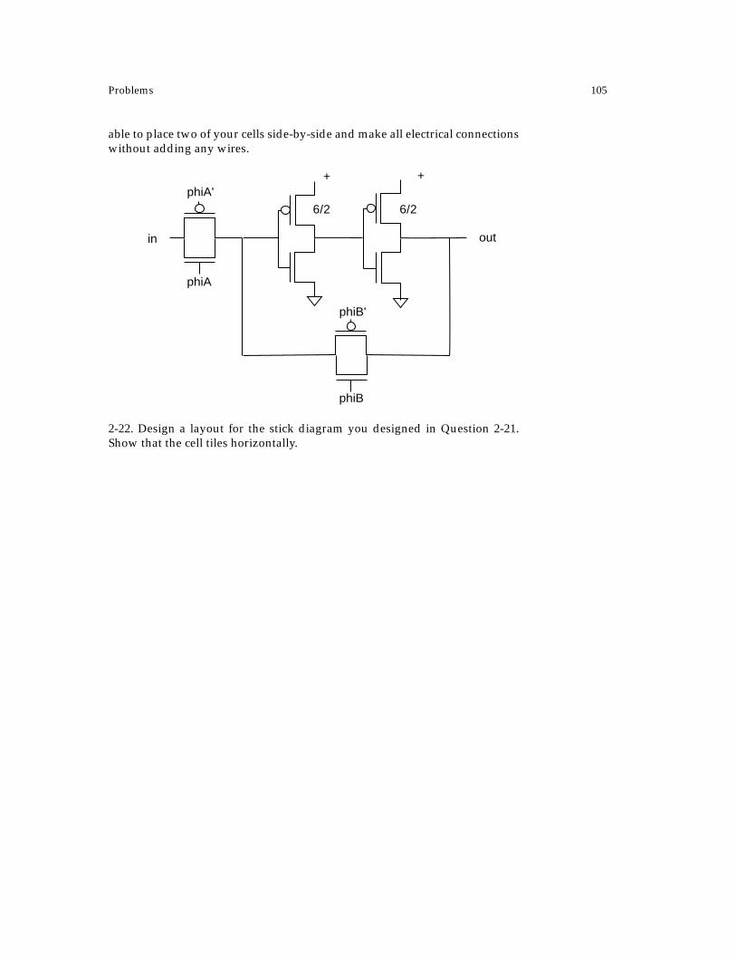
Problems 105
able to place two of your cells side-by-side and make all electrical connectionswithout adding any wires.
2-22. Design a layout for the stick diagram you designed in Question 2-21.Show that the cell tiles horizontally.
+ +
in out
phiA'
phiB'
phiA
phiB
6/26/2

106 Transistors and Layout