tps65270 loop compensation design consideration · slva510– april 2012 tps65270 loop compensation...
TRANSCRIPT

Application ReportSLVA510–April 2012
TPS65270 Loop Compensation Design ConsiderationTony Huang .................................................................... Power Management Products/Filed Applications
ABSTRACT
Peak current mode (PCM) is a popular, affordable, and stable control mode. This report discusses thecontrol principle and small signal model, as well as the stability and loop compensation approach forTPS65270.
Contents1 Introduction .................................................................................................................. 22 PCM Principle and Modeling .............................................................................................. 2
2.1 PCM Behavior ...................................................................................................... 22.2 Overall Control Block Diagram Implementation ................................................................ 32.3 Small Signal Model of the TPS65270 Synchronous BUCK Converter ...................................... 32.4 Transfer Function Derivation from the Average Mode and the Small Signal Model ...................... 42.5 Inductor Current Sampling-Hold and Slope Compensation .................................................. 52.6 Simplify the Current Loop Parameters .......................................................................... 6
3 TPS65270 Modeling and Loop Compensation .......................................................................... 73.1 Results vs Simulation Based on a Practical Design ........................................................... 73.2 Simulation for a Specific Design ................................................................................. 9
4 Conclusion .................................................................................................................. 115 References ................................................................................................................. 11
List of Figures
1 TPS65270 Block Diagram ................................................................................................. 2
2 PCM Implementation ....................................................................................................... 3
3 Overall Control Implementation ........................................................................................... 3
4 Average Model .............................................................................................................. 3
5 Small Signal Model ......................................................................................................... 3
6 PWM with Slope Compensation .......................................................................................... 4
7 Practical Sampling-Hold Waveforms with the Current and Control Distortion ...................................... 5
8 Approximated Sampling-Hold Waveforms with the Current and Control Distortion ................................ 5
9 Control Block for Current Regulation Loop .............................................................................. 6
10 Equivalent Small Signal Model ............................................................................................ 7
11 TPS65270 Design with 3.3- and 7.7-V Output .......................................................................... 7
12 Overall Small Signal Modeling for TPS65270 with 3.3-V/0.65-A Output ............................................ 8
13 Bode Plot of the AC Simulation ........................................................................................... 8
14 Closed Loop Bode Plot Test Results at Vin = 12 V and Vout = 3.3 V/0.65 A ...................................... 9
15 Signal Modeling From Control to Output................................................................................. 9
16 Bode Plot of Control to Output........................................................................................... 10
17 Overall Small Signal Modeling........................................................................................... 11
18 Overall Gain and Phase Bode Plot...................................................................................... 11
List of Tables
1 Modeling Parameters....................................................................................................... 9
1SLVA510–April 2012 TPS65270 Loop Compensation Design ConsiderationSubmit Documentation Feedback
Copyright © 2012, Texas Instruments Incorporated

C8
IUM
180°
Logic
InternalLDO
OSC
LOW_P 5
6
8
VCC
ROSC
SS1 3
2
4
FB1FB1
COMP1
EN1 1EN1 Logic
EN2 LogicEN2
12
9
11
10
COMP2
FB2FB2
SS2
AGND 8
23 VIN1VIN1
24 BST1
LX121,22
19,20 GND
FB1
BUCK 1
17,18
15,16
GND
LX2
FB2
Same as Buck 1
BUCK 2BST2
VIN2VIN2
VOUT BUCK1
VOUT BUCK2
+
–
–
+
SLP
EA0.8V
COMP
S
REN
Q
Q
13
14
Pre-regulator, Voltage Reference,Current Bias
Latch
Introduction www.ti.com
1 Introduction
TPS65270 is a dual channel DCDC with peak current mode (PCM) implementation. The integratedsynchronous rectifier power FET, as well as the novel power save mode, power-up sequence, and over-current protection configuration, benefit the customer design with high flexibility, efficiency, and morecompact size.
This dual DCDC is designed with 5- to 16-V wide input, and a loading capability of up to 3/2 A outputcurrents. It is all MOSFET integrated, has individual SS and EN pins, adjusted frequency (300 kHz ~ 1.4MHz), automatic Power-Save-Mode for light load operations and 24-pin TSSOP and 24-pin 4 × 4 mmQFN.
Figure 1. TPS65270 Block Diagram
2 PCM Principle and Modeling
2.1 PCM Behavior
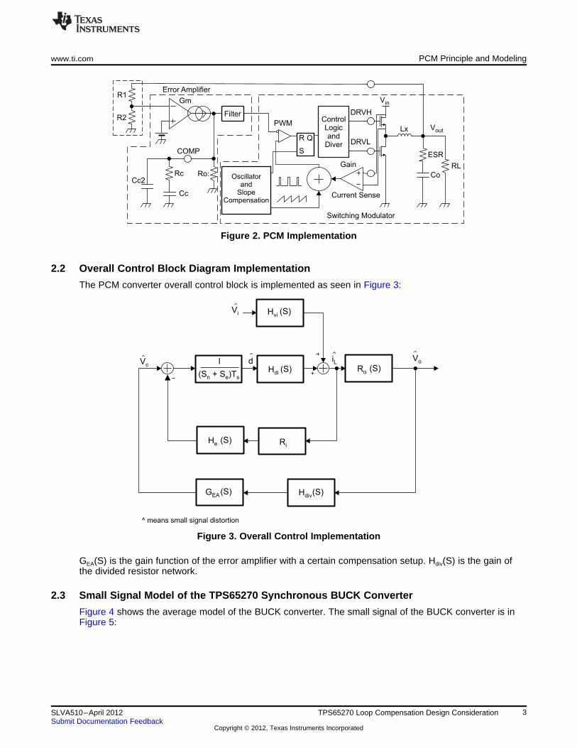
PCM employs a current-sampling RAMP to compare with the output of the Error Amplifier (EA), thereforegenerating the regulated duty cycle as shown in Figure 2. PCM initiates the fast response by input orloading transient with current and voltage loops, achieving higher crossover frequency.
2 TPS65270 Loop Compensation Design Consideration SLVA510–April 2012Submit Documentation Feedback
Copyright © 2012, Texas Instruments Incorporated
Vi (S)Hvi
iLd(S)Hdi
(S)Ro
VoVc
Ri(S)He
(S)GEA (S)Hdiv
l
(S + S )Tn e s
^ means small signal distortion
R1
R2
Gm
Error Amplifier
Filter
Cc2
Cc
Rc Ro:
COMP
Oscillatorand
SlopeCompensation
PWM
R
S
Q
ControlLogicand
Diver
DRVH
DRVL
Gain
Current Sense
Vin
Lx Vout
ESR
Co
RL
Switching Modulator
www.ti.com PCM Principle and Modeling
Figure 2. PCM Implementation
2.2 Overall Control Block Diagram Implementation
The PCM converter overall control block is implemented as seen in Figure 3:
Figure 3. Overall Control Implementation
GEA(S) is the gain function of the error amplifier with a certain compensation setup. Hdiv(S) is the gain ofthe divided resistor network.
2.3 Small Signal Model of the TPS65270 Synchronous BUCK Converter
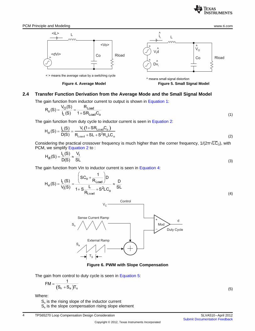
Figure 4 shows the average model of the BUCK converter. The small signal of the BUCK converter is inFigure 5:
3SLVA510–April 2012 TPS65270 Loop Compensation Design ConsiderationSubmit Documentation Feedback
Copyright © 2012, Texas Instruments Incorporated
( )n e s
1 FM
S S T=
+
VC
Control
Sense Current Ramp
Sn
Se
External Ramp
TS
Mod
+ d
Duty Cycle–
oLoadL
vi2I
oLoad
1SC D
RI (S) DH (S)
LV(S) SL1 S S LC
R
æ ö+ç ÷
è ø= = »
+ +
L Idi
I (S) V H (S)
D(S) SL= »
( )I Lo ad oLdi 2
Loa d o o
V 1 SR CI (S)H (S)
D(S) R SL S R LC
+= =
+ +
O Loado
L Load o
V (S) R R (S)
I (S) 1 SR C= =
+
iL L
Co Rload
V dI
Dvi
VO
^ means small signal distortion
^
^^
^
<iL> L
<Vo>
Co Rload<dVi>
< > means the average value by a switching cycle
PCM Principle and Modeling www.ti.com
Figure 4. Average Model Figure 5. Small Signal Model
2.4 Transfer Function Derivation from the Average Mode and the Small Signal Model
The gain function from inductor current to output is shown in Equation 1:
(1)
The gain function from duty cycle to inductor current is seen in Equation 2:
(2)
Considering the practical crossover frequency is much higher than the corner frequency, 1/(2π√LCO), withPCM, we simplify Equation 2 to :
(3)
The gain function from Vin to inductor current is seen in Equation 4:
(4)
Figure 6. PWM with Slope Compensation
The gain from control to duty cycle is seen in Equation 5:
(5)
Where:Sn is the rising slope of the inductor currentSe is the slope compensation rising slope element
4 TPS65270 Loop Compensation Design Consideration SLVA510–April 2012Submit Documentation Feedback
Copyright © 2012, Texas Instruments Incorporated

f e
n e
S S
S S
-
a =
+
^^
cL Li
^ 1(K 1) (k) v (k 1)i i
R (1 )+ = -a + +
+ a
Approximate
i (k)s
sn sf
VC VC+
se
(a)
(b)
i (n)s
k k+1t
^ means small signal distortion
Practical
i (k)s
sn sf
VC VC+
se
(a)
(b)
i (n)s
k k+1t
^ means small signal distortion
www.ti.com PCM Principle and Modeling
Ts is the switching cycleConsidering the sampling-hold circuitry for the current ramp, the gain function is He(S):
2.5 Inductor Current Sampling-Hold and Slope Compensation
The Ridley sampling-hold model is shown in Figure 7 and Figure 8:
Figure 7. Practical Sampling-Hold Waveforms with the Current and Control Distortion
Figure 8. Approximated Sampling-Hold Waveforms with the Current and Control Distortion
The discrete equation is derived to describe the sampling-hold behavior in Equation 6:
(6)
Here: Where:
Sf is the inductor current ramp down slope.
Sn is the rising slope of the inductor currentSe is the slope compensation rising slope element
5SLVA510–April 2012 TPS65270 Loop Compensation Design ConsiderationSubmit Documentation Feedback
Copyright © 2012, Texas Instruments Incorporated

si
e
(1 D)TD L F
L R 2
é ù-= -ê ú
ë û
2
se e 2
s
T2L Let : R : C
2 LT 1
1
= =æ ö p-ç ÷+ aè ø
( ) 2i s n e 2s s
2I i
1 1H(S)
R T L S S T T1 S S
VR 2´
» ´é ù+
+ - +ê úpê úë û
s
2s
e T S 2
ss
T S S SAs a result : H (S) 1
2e 1T
T
= » - +- æ öp
ç ÷è ø
VC l d iL(S)Hdi
(S)He Ri
(S + S )Tn e s
^ ^ ^
^ means small signal distortion
s s s
s s
T S T S T S
T S T Si s i s
1 e 1 e 1 e 1H(S)
R T S R T Se e
-+ a - + a -
= ´ ´ = ´
+ a + a
sT S
s
1 e
T S
-
-
L
c i
I (Z) 1 Z H(Z)
V (Z) R Z
+ a= = ´
+ a
PCM Principle and Modeling www.ti.com
Based on the discrete sampling model, Z, domain translation results should be:
(7)
Based on Z domain stability theory, the single pole should meet this condition: | α | < 1
As a result, the slope compensation element, Se, should adequately meet: Se > Sn / 2
With substituting “Z” with “eTsS” and considering zero order sampling-hold gain , the gain functionis seen in Equation 8:
(8)
According to Figure 6, the H(S) is described as Figure 9, considering Equation 3 for Hdi(S)
Figure 9. Control Block for Current Regulation Loop
(9)
2.6 Simplify the Current Loop Parameters
Based on Equation 9 and Equation 10, the approximate gain from control to inductor current should be:
(10)
(11)
And considering Equation 4, let:
then the current loop is simplified as shown in Figure 10:
6 TPS65270 Loop Compensation Design Consideration SLVA510–April 2012Submit Documentation Feedback
Copyright © 2012, Texas Instruments Incorporated

GND C116
100pF
C249
2.2nF
R127 R126
10K 383K
C250
10µF
2.2nF
C248C119
30K
R125 270pF
U11 24
23
22
21
20
19
1
2
3
4
5
6
18
17
16
15
14
13
7 8 9
10 11
12
LX
2
LX
1
LX1LX2
GN
D
GN
D
GN
D
GN
D
FB2
EN2
SS2
BST2
VIN2
SS1
FB1
EN1
BST1
VIN1
CO
MP
2
RO
SC
AG
ND
VC
C
LO
W_
P
CO
MP
1
TPS65270
10nFC53
C165 4.7nF
C148 47nF
R157
GND
C152 47nF
GND
00
C153
4.7nFEN_7.7V
C173
10µF R105
L5
L9
VCC
C154
6.8µH
4.7µH
10µF
CNI
GND
TPS65270
GN
D
R124
C247
82pFC155
10µF
86.6K
R123
10K
+ C189
470µF
0
R174
+7.7V
GND
GND
10nF
C191 C190
10µF
CNICNI
+3.3V
R253
0
C361+ C258
10µF470µF 100nF
C396 C395
22µF
CNI
10K
GND
GND
GN
D VCC
10µF
L6
L16
6.8µH
4.7µH
CNI
22µF82pF
R122
C151
C150 C148
31.6K
R120
e
s
2L If : R 0
2T 1
1
= >æ ö
-ç ÷+ aè ø
Re Ce Co Rload
L VO
iL
FiVi
Ri
VC
^ means small signal distortion
^
^
^^
www.ti.com TPS65270 Modeling and Loop Compensation
Figure 10. Equivalent Small Signal Model
Figure 10 reveals an internal resistance, Re and Ce, in the small signal model:
(12)
Then: 0 < 1 + α < 2; Or |α| < 1
As a result Se > Sn / 2
In conclusion, the PCM small signal model is simplified as shown in Figure 10. Meanwhile, a positive Re
brings up a stable system without the sub-harmonic oscillation, which is reached by a certain amount ofslope compensation. The simplified model is more feasibly simulated with EDA tools.
3 TPS65270 Modeling and Loop Compensation
3.1 Results vs Simulation Based on a Practical Design
Figure 11. TPS65270 Design with 3.3- and 7.7-V Output
Figure 11 shows the frequency is 635 kHz, input is 12 V and output is 3.3 V/2 A and 7.7 V/1 A.
For channel 2 with 3.3-V output:
7SLVA510–April 2012 TPS65270 Loop Compensation Design ConsiderationSubmit Documentation Feedback
Copyright © 2012, Texas Instruments Incorporated
80
60
40
20
0
–20
–40
–60
200
100
0
–100
–20010 100 1k 10k 100k 1M
Gain
(dB
)P
hase (
deg)
Frequency (Hz)
-
++3
2
6
7
4
EA
Rgm 7.69k
C3 560p
V–
+
Vos
V
+
Vo
ISNS 1
Co 22u Rload 1.65
R1 18.8k
C16 56p
AcsRs 100m
R4a 40.2k
R4b 12.8k
C11 82p
L 4.7u
Re 3.03 Ce
V(+)
59.88n
f e
n e
S S 0.427
S S
-
a = = -
+
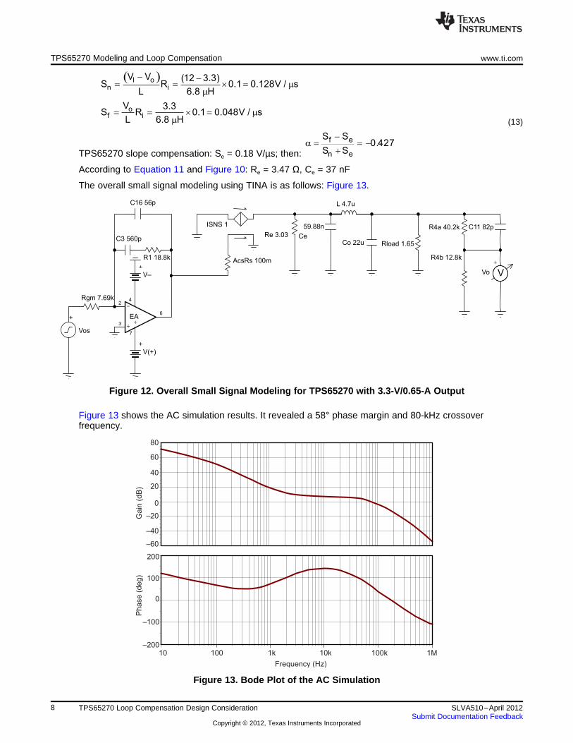
( )I on i
of i
V V (12 3.3)S R 0.1 0.128V / s
L 6.8 H
V 3.3S R 0.1 0.048V / s
L 6.8 H
- -= = ´ = m
m
= = ´ = mm
TPS65270 Modeling and Loop Compensation www.ti.com
(13)
TPS65270 slope compensation: Se = 0.18 V/µs; then:
According to Equation 11 and Figure 10: Re = 3.47 Ω, Ce = 37 nF
The overall small signal modeling using TINA is as follows: Figure 13.
Figure 12. Overall Small Signal Modeling for TPS65270 with 3.3-V/0.65-A Output
Figure 13 shows the AC simulation results. It revealed a 58° phase margin and 80-kHz crossoverfrequency.
Figure 13. Bode Plot of the AC Simulation
8 TPS65270 Loop Compensation Design Consideration SLVA510–April 2012Submit Documentation Feedback
Copyright © 2012, Texas Instruments Incorporated

V
+
Vo
ISNS 1
Co 22u Rload 1.65
AcsRs 100m
R4a 40.2k
R4b 12.8k
C11 82p
L 4.7u
Re 3.03Ce 59.88n
+Vc
^ means small signal distortion
www.ti.com TPS65270 Modeling and Loop Compensation
The practical test results for the 3.3 V/0.65 A are shown in Figure 14:
Figure 14. Closed Loop Bode Plot Test Results at Vin = 12 V and Vout = 3.3 V/0.65 A
The loop parameters in Figure 14 are 86-kHz crossover frequency and 60° phase margin.
The model shown in Figure 10 is used in PCM loop compensation.
3.2 Simulation for a Specific Design
A design topic: Vin = 12 V, Vout = 3.3 V at 2 A, fs = 600 kHz, L = 4.7 µH
The related parameters are shown in Table 1:
Table 1. Modeling Parameters
Vin (V) Vout (V) L (µH) f (kHz) Ri Se (V/µs)
12 3.3 4.7 600 0.1 0.18
Sn(V/µs) Sf(V/µs) α Re Ce(nF)
0.19 0.07 –0.30 3.03 59.88
The small signal modeling from control to output:
Figure 15. Signal Modeling From Control to Output
9SLVA510–April 2012 TPS65270 Loop Compensation Design ConsiderationSubmit Documentation Feedback
Copyright © 2012, Texas Instruments Incorporated

10
3 c
K R 18.8 k
2 C= = W
p ¦
gmc gm
K 1 1 And : ; R 7.69 k
A 2 ƒ R C 130u7
= = = Wp
( )6.9
20co c
70 ( 78 ) 90 Let : A G j2 10 0.45; K tg 45 3.5
2
-- ° - - ° - °æ ö
= p¦ = = = + ° =ç ÷è ø
T
Gain
(dB
)
–50
–40
–30
–20
–10
0
10
Frequency (Hz)
10 100 1k 10k 100k 1M
Phase (
deg)
-300
–200
–100
0
a
b
TPS65270 Modeling and Loop Compensation www.ti.com
The simulation reveals the bode plot in Figure 16.
Assuming a target crossover frequency is 50 kHz, and target phase margin is 70°.
According to the bode plot in Figure 16:
Gco(50 kHz) = –6.87 dB; Phaseco (50 kHz) = –77°
Figure 16. Bode Plot of Control to Output
The Type II compensation network setup:
Assume a crossover frequency of fc = 50 kHz.
Then: C16 = 52.9 pF, select C16 = 56 pF, C3 = (K2 – 1), C16 = 590 pF, select C3 = 560 pF:
As a result in Figure 17 and Figure 18, the final crossover frequency is 49 kHz and the phase margin is69°.
10 TPS65270 Loop Compensation Design Consideration SLVA510–April 2012Submit Documentation Feedback
Copyright © 2012, Texas Instruments Incorporated

T
Gain
(dB
)
–80
–60
–40
–20
0
20
40
60
80
Frequency (Hz)
10 100 1k 10k 100k 1M
Phase (
deg)
–200
–100
0
100
200
a
b
–
+ +3
2
6
7
4
EA
Rgm 7.69k
C3 2.2n
V–
+
Vos
V
+
Vo
ISNS 1
Co 470u
Rload 5.1
R1 30k
C16 100p
AcsRs 100m
R4a 31.6k
R4b 10k
C11 82p
L 6.8u
Re 3.47 Ce 37n
V(+)
Esr 300m C1 10u
www.ti.com Conclusion
Figure 17. Overall Small Signal Modeling
Figure 18. Overall Gain and Phase Bode Plot
4 Conclusion
This application note introduces a practical modeling approach for PCM control using TPS65270. A simpleequivalent circuit representation is shown for easy understanding and implementation of peak current-mode control. Simulation results are used to demonstrate the proposed model.
5 References1. TPS65270 datasheet , (SLVSAX07A), Texas Instruments
2. Tony Huang, Floating Buck-Boost LED Driver Control-Loop Analysis, (SLVA312), Texas Instruments
3. R. B. Ridley, A new, continuous-time model for current-mode control, IEEE Trans. Power Electron., vol.6, no. 2, pp. 271-280, April 1991.
4. L. H. Dixon, Average Current-Mode Control of Switching Power Supplies,” Unitrode Power Supply
11SLVA510–April 2012 TPS65270 Loop Compensation Design ConsiderationSubmit Documentation Feedback
Copyright © 2012, Texas Instruments Incorporated

References www.ti.com
Design Seminar handbook, 1990, pp. 5.1-5.14.
5. Jian Li, Fred C. Lee, New Modeling Approach for Current-Mode Control, 2009 IEEE.
12 TPS65270 Loop Compensation Design Consideration SLVA510–April 2012Submit Documentation Feedback
Copyright © 2012, Texas Instruments Incorporated

IMPORTANT NOTICE
Texas Instruments Incorporated and its subsidiaries (TI) reserve the right to make corrections, modifications, enhancements, improvements,and other changes to its products and services at any time and to discontinue any product or service without notice. Customers shouldobtain the latest relevant information before placing orders and should verify that such information is current and complete. All products aresold subject to TI’s terms and conditions of sale supplied at the time of order acknowledgment.
TI warrants performance of its hardware products to the specifications applicable at the time of sale in accordance with TI’s standardwarranty. Testing and other quality control techniques are used to the extent TI deems necessary to support this warranty. Except wheremandated by government requirements, testing of all parameters of each product is not necessarily performed.
TI assumes no liability for applications assistance or customer product design. Customers are responsible for their products andapplications using TI components. To minimize the risks associated with customer products and applications, customers should provideadequate design and operating safeguards.
TI does not warrant or represent that any license, either express or implied, is granted under any TI patent right, copyright, mask work right,or other TI intellectual property right relating to any combination, machine, or process in which TI products or services are used. Informationpublished by TI regarding third-party products or services does not constitute a license from TI to use such products or services or awarranty or endorsement thereof. Use of such information may require a license from a third party under the patents or other intellectualproperty of the third party, or a license from TI under the patents or other intellectual property of TI.
Reproduction of TI information in TI data books or data sheets is permissible only if reproduction is without alteration and is accompaniedby all associated warranties, conditions, limitations, and notices. Reproduction of this information with alteration is an unfair and deceptivebusiness practice. TI is not responsible or liable for such altered documentation. Information of third parties may be subject to additionalrestrictions.
Resale of TI products or services with statements different from or beyond the parameters stated by TI for that product or service voids allexpress and any implied warranties for the associated TI product or service and is an unfair and deceptive business practice. TI is notresponsible or liable for any such statements.
TI products are not authorized for use in safety-critical applications (such as life support) where a failure of the TI product would reasonablybe expected to cause severe personal injury or death, unless officers of the parties have executed an agreement specifically governingsuch use. Buyers represent that they have all necessary expertise in the safety and regulatory ramifications of their applications, andacknowledge and agree that they are solely responsible for all legal, regulatory and safety-related requirements concerning their productsand any use of TI products in such safety-critical applications, notwithstanding any applications-related information or support that may beprovided by TI. Further, Buyers must fully indemnify TI and its representatives against any damages arising out of the use of TI products insuch safety-critical applications.
TI products are neither designed nor intended for use in military/aerospace applications or environments unless the TI products arespecifically designated by TI as military-grade or "enhanced plastic." Only products designated by TI as military-grade meet militaryspecifications. Buyers acknowledge and agree that any such use of TI products which TI has not designated as military-grade is solely atthe Buyer's risk, and that they are solely responsible for compliance with all legal and regulatory requirements in connection with such use.
TI products are neither designed nor intended for use in automotive applications or environments unless the specific TI products aredesignated by TI as compliant with ISO/TS 16949 requirements. Buyers acknowledge and agree that, if they use any non-designatedproducts in automotive applications, TI will not be responsible for any failure to meet such requirements.
Following are URLs where you can obtain information on other Texas Instruments products and application solutions:
Products Applications
Audio www.ti.com/audio Automotive and Transportation www.ti.com/automotive
Amplifiers amplifier.ti.com Communications and Telecom www.ti.com/communications
Data Converters dataconverter.ti.com Computers and Peripherals www.ti.com/computers
DLP® Products www.dlp.com Consumer Electronics www.ti.com/consumer-apps
DSP dsp.ti.com Energy and Lighting www.ti.com/energy
Clocks and Timers www.ti.com/clocks Industrial www.ti.com/industrial
Interface interface.ti.com Medical www.ti.com/medical
Logic logic.ti.com Security www.ti.com/security
Power Mgmt power.ti.com Space, Avionics and Defense www.ti.com/space-avionics-defense
Microcontrollers microcontroller.ti.com Video and Imaging www.ti.com/video
RFID www.ti-rfid.com
OMAP Mobile Processors www.ti.com/omap
Wireless Connectivity www.ti.com/wirelessconnectivity
TI E2E Community Home Page e2e.ti.com
Mailing Address: Texas Instruments, Post Office Box 655303, Dallas, Texas 75265Copyright © 2012, Texas Instruments Incorporated