tps56528 4.5-v to 18-v input, 5-a synchronous step-down
TRANSCRIPT
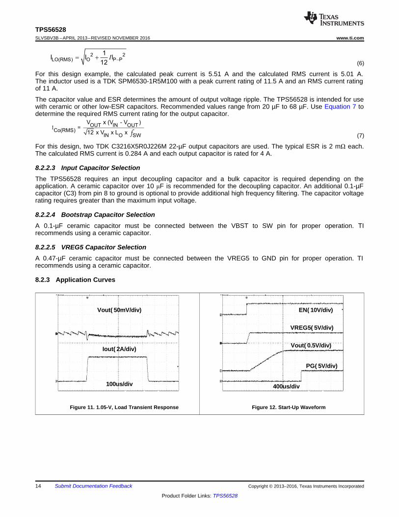
Vout( 50mV/div)
Iout( 2A/div)
100us/div
TPS56528
Copyright © 2016, Texas Instruments Incorporated
Product
Folder
Sample &Buy
Technical
Documents
Tools &
Software
Support &Community
ReferenceDesign
An IMPORTANT NOTICE at the end of this data sheet addresses availability, warranty, changes, use in safety-critical applications,intellectual property matters and other important disclaimers. PRODUCTION DATA.
TPS56528SLVSBV3B –APRIL 2013–REVISED NOVEMBER 2016
TPS56528 4.5-V to 18-V Input, 5-A Synchronous Step-Down ConverterWith Advanced Eco-Mode™
1
1 Features1• D-CAP2™ Mode Enables Fast Transient
Response• Low Output Ripple and Allows Ceramic Output
Capacitor• Wide VIN Input Voltage Range: 4.5 V to 18 V• Output Voltage Range: 0.6 V to 7 V• Highly Efficient Integrated FETs Optimized
for Lower Duty Cycle Applications–68 mΩ (High-Side) and 37 mΩ (Low-Side)
• High Efficiency, Less Than 10 µA at Shutdown• High Initial Band-Gap Reference Accuracy• Prebiased Soft Start• 650-kHz Switching Frequency (fSW)• Cycle-By-Cycle Overcurrent Limit• Advanced Auto-Skip Eco-Mode™ for High
Efficiency at Light Load• Power Good Output• Fixed Soft Start: 1 ms
2 Applications• Wide Range of Applications for Low Voltage
Systems– Digital TV Power Supply– High Definition Blu-ray Disc™ Players– Networking Home Terminals– Digital Set-Top Boxes (STB)
3 DescriptionThe TPS56528 device is an adaptive on-timeD-CAP2™ mode synchronous buck converter. TheTPS56528 enables system designers to complete thesuite of various end-equipment power bus regulatorswith a cost-effective, low component count, lowstandby current solution. The main control loop forthe TPS56528 uses the D-CAP2™ mode control thatprovides a fast transient response with no externalcompensation components. The adaptive on-timecontrol supports seamless transition between PWMmode at higher load conditions and advanced Eco-Mode™ operation at light loads. Advanced Eco-Mode™ allows the TPS56528 to maintain highefficiency during lighter load conditions. TheTPS56528 also has a proprietary circuit that enablesthe device to adopt to both low equivalent seriesresistance (ESR) output capacitors, such asPOSCAP or SP-CAP, and ultra-low ESR ceramiccapacitors. The device operates from 4.5-V to 18-VVIN input. The output voltage can be programmedbetween 0.6 V and 7 V. The device also features afixed 1-ms soft-start time and power good output. TheTPS56528 is available in the 8-pin SO PowerPAD™package, and designed to operate from –40°C to85°C.
Device Information(1)
PART NUMBER PACKAGE BODY SIZE (NOM)TPS56528 SO PowerPAD (8) 4.89 mm × 3.90 mm
(1) For all available packages, see the orderable addendum atthe end of the data sheet.
Simplified Schematic Transient Response
2
TPS56528SLVSBV3B –APRIL 2013–REVISED NOVEMBER 2016 www.ti.com
Product Folder Links: TPS56528
Submit Documentation Feedback Copyright © 2013–2016, Texas Instruments Incorporated
Table of Contents1 Features .................................................................. 12 Applications ........................................................... 13 Description ............................................................. 14 Revision History..................................................... 25 Pin Configuration and Functions ......................... 36 Specifications......................................................... 4
6.1 Absolute Maximum Ratings ...................................... 46.2 ESD Ratings.............................................................. 46.3 Recommended Operating Conditions....................... 46.4 Thermal Information .................................................. 56.5 Electrical Characteristics........................................... 56.6 Timing Requirements ................................................ 66.7 Typical Characteristics .............................................. 7
7 Detailed Description .............................................. 97.1 Overview ................................................................... 97.2 Functional Block Diagram ......................................... 97.3 Feature Description................................................. 107.4 Device Functional Modes........................................ 11
8 Application and Implementation ........................ 128.1 Application Information............................................ 128.2 Typical Application ................................................. 12
9 Power Supply Recommendations ...................... 1510 Layout................................................................... 16
10.1 Layout Guidelines ................................................. 1610.2 Layout Example .................................................... 1610.3 Thermal Information .............................................. 17
11 Device and Documentation Support ................. 1811.1 Device Support...................................................... 1811.2 Documentation Support ....................................... 1811.3 Receiving Notification of Documentation Updates 1811.4 Community Resources.......................................... 1811.5 Trademarks ........................................................... 1811.6 Electrostatic Discharge Caution............................ 1811.7 Glossary ................................................................ 18
12 Mechanical, Packaging, and OrderableInformation ........................................................... 18
4 Revision HistoryNOTE: Page numbers for previous revisions may differ from page numbers in the current version.
Changes from Revision A (April 2013) to Revision B Page
• Added Pin Configuration and Functions section, ESD Ratings table, Feature Description section, Device FunctionalModes, Application and Implementation section, Power Supply Recommendations section, Layout section, Deviceand Documentation Support section, and Mechanical, Packaging, and Orderable Information section .............................. 1
Changes from Original (April 2013) to Revision A Page
• Changed the device From: Product Preview To: Production ................................................................................................. 1
1EN 8 VIN
2VFB 7 VBST
3VREG5 6 SW
4PG 5 GND
Not to scale
PowerPAD
3
TPS56528www.ti.com SLVSBV3B –APRIL 2013–REVISED NOVEMBER 2016
Product Folder Links: TPS56528
Submit Documentation FeedbackCopyright © 2013–2016, Texas Instruments Incorporated
5 Pin Configuration and Functions
DDA Package8-Pin SO PowerPAD
Top View
Pin FunctionsPIN
I/O DESCRIPTIONNO. NAME1 EN I Enable input control. EN is active high and must be pulled up to enable the device.2 VFB I Converter feedback input. Connect to output voltage with feedback resistor divider.
3 VREG5 O 5.5-V power supply output. A capacitor (0.47 µF typical) must be connected to GND. VREG5 is notactive when EN is low.
4 PG O Open-drain power good output.
5 GND — Ground pin. Power ground return for switching circuit. Connect sensitive SS and VFB returns toGND at a single point.
6 SW O Switch node connection between high-side NFET and low-side NFET.
7 VBST O Supply input for the high-side FET gate drive circuit. Connect 0.1-µF capacitor between VBST andSW pins. An internal diode is connected between VREG5 and VBST.
8 VIN I Input voltage supply pin.
— PowerPAD — Thermal pad of the package. This pad must be soldered to achieve appropriate dissipation andmust be connected to GND.
4
TPS56528SLVSBV3B –APRIL 2013–REVISED NOVEMBER 2016 www.ti.com
Product Folder Links: TPS56528
Submit Documentation Feedback Copyright © 2013–2016, Texas Instruments Incorporated
(1) Stresses beyond those listed under Absolute Maximum Ratings may cause permanent damage to the device. These are stress ratingsonly, and functional operation of the device at these or any other conditions beyond those indicated under Recommended OperatingConditions is not implied. Exposure to absolute-maximum-rated conditions for extended periods may affect device reliability.
6 Specifications
6.1 Absolute Maximum Ratingsover operating free-air temperature range (unless otherwise noted) (1)
MIN MAX UNIT
Input voltage
VIN and EN –0.3 20
V
VBST –0.3 26VBST (10-ns-transient) –0.3 28VBST (vs SW) –0.3 6.5VFB and PG –0.3 6.5SW –2 20SW (10-ns-transient) –3 22
Output voltageVREG5 –0.3 6.5
VGND –0.3 0.3
Voltage from GND to thermal pad, Vdiff –0.2 0.2 VOperating junction temperature, TJ –40 150
°CStorage temperature, Tstg –55 150
(1) JEDEC document JEP155 states that 500-V HBM allows safe manufacturing with a standard ESD control process.(2) JEDEC document JEP157 states that 250-V CDM allows safe manufacturing with a standard ESD control process.
6.2 ESD RatingsVALUE UNIT
V(ESD) Electrostatic dischargeHuman body model (HBM), per ANSI/ESDA/JEDEC JS-001 (1) ±2000
VCharged-device model (CDM), per JEDEC specification JESD22-C101 (2) ±500
6.3 Recommended Operating Conditionsover operating free-air temperature range (unless otherwise noted)
MIN MAX UNITVIN Supply input voltage 4.5 18 V
VI Input voltage
VBST –0.1 24
V
VBST (10-ns-transient) –0.1 27VBST(vs SW) –0.1 6PG –0.1 5.7EN –0.1 18VFB –0.1 5.5SW –1.8 18SW (10-ns-transient) –3 21GND –0.1 0.1
VO Output voltage (VREG5) –0.1 5.7 VIO Output current (IVREG5) 0 5 mATA Operating free-air temperature –40 85 °CTJ Operating junction temperature –40 150 °C

5
TPS56528www.ti.com SLVSBV3B –APRIL 2013–REVISED NOVEMBER 2016
Product Folder Links: TPS56528
Submit Documentation FeedbackCopyright © 2013–2016, Texas Instruments Incorporated
(1) For more information about traditional and new thermal metrics, see the Semiconductor and IC Package Thermal Metrics applicationreport.
6.4 Thermal Information
THERMAL METRIC (1)TPS56528
UNITDDA (SO PowerPAD)8 PINS
RθJA Junction-to-ambient thermal resistance 44.4 °C/WRθJCtop Junction-to-case (top) thermal resistance 51.6 °C/WRθJB Junction-to-board thermal resistance 27.8 °C/WψJT Junction-to-top characterization parameter 8.7 °C/WψJB Junction-to-board characterization parameter 27.7 °C/WRθJCbot Junction-to-case (bottom) thermal resistance 5.3 °C/W
(1) Not production tested.
6.5 Electrical Characteristicsover operating free-air temperature range, VIN = 12 V (unless otherwise noted)
PARAMETER TEST CONDITIONS MIN TYP MAX UNITSUPPLY CURRENT
I(VIN) Operating non-switching supply current VIN current, TA = 25°C, EN = 5 V,V(FB) = 0.7 V 170 350 μA
I(VINSDN) Shutdown supply current VIN current, TA = 25°C, EN = 0 V 3.8 10 µALOGIC THRESHOLD
V(EN)EN high-level input voltage EN 1.6 VEN low-level input voltage EN 0.6 V
R(EN) EN pin resistance to GND VEN = 12 V 180 350 700 kΩVFB VOLTAGE AND DISCHARGE RESISTANCE
V(FBTH) V(FB) threshold voltage
TA = 25°C, VO = 1.05 V, IO = 10 mA, advancedEco-Mode operation 606 mV
TA = 25°C, VO = 1.05 V, continuous modeoperation 593 600 607 mV
TA = -40 to 85°C, VO = 1.05 V, continuousmode operation (1) 588 600 612 mV
I(VFB) V(FB) input current V(FB) = 0.7 V, TA = 25°C 0 ±0.15 µASW DISCHARGEI(DISCHG) SW discharge current EN = 0 V, SW = 1 V, TA = 25°C 1 1.5 mAV(REG5) OUTPUT
V(VREG5) VREG5 output voltage TA = 25°C, 6.0 V < VIN < 18 V,0 < I(VREG5) < 5 mA 5.2 5.5 5.7 V
I(VREG5) Output current VIN = 6 V, V(REG5) = 4 V, TA = 25°C 20 mAMOSFET
RDS(on)High-side switch resistance 25°C, V(BST) - SW = 5.5 V 68 mΩ
Low-side switch resistance 25°C 37 mΩ
CURRENT LIMITI(ocl) Current limit LOUT = 1.5 µH (1) 5.5 6.2 7.8 ATHERMAL SHUTDOWN
T(SDN) Thermal shutdown thresholdShutdown temperature (1) 165
°CHysteresis (1) 35
POWER GOOD
V(THPG) PG thresholdVFB rising (good) 85% 90% 95%VFB falling (Fault) 85%
IPG PG sink current PG = 0.5 V 2 4 mA

6
TPS56528SLVSBV3B –APRIL 2013–REVISED NOVEMBER 2016 www.ti.com
Product Folder Links: TPS56528
Submit Documentation Feedback Copyright © 2013–2016, Texas Instruments Incorporated
Electrical Characteristics (continued)over operating free-air temperature range, VIN = 12 V (unless otherwise noted)
PARAMETER TEST CONDITIONS MIN TYP MAX UNITOUTPUT UNDERVOLTAGE AND OVERVOLTAGE PROTECTIONVOVP Output OVP threshold OVP Detect (L>H) 125%VUVP Output UVP threshold UVP detect (H>L) 65%UVLO
UVLO UVLO thresholdWake-up VREG5 voltage 3.45 3.75 4.05
VHysteresis VREG5 voltage 0.13 0.32 0.48
6.6 Timing RequirementsMIN NOM MAX UNIT
ON-TIME TIMER CONTROLtON On-time VIN = 12 V, VO = 1.05 V 150 nstOFF(MIN) Minimum off-time TA = 25°C, VFB = 0.5 V 260 310 nsSOFT STARTtSS Soft-start time Internal soft-start time 0.7 1 1.3 msOUTPUT UNDERVOLTAGE AND OVERVOLTAGE PROTECTIONtUVPDEL Output UVP delay to hiccup state 7
µstUVPEN Output UVP enable delay Relative to soft-start time ×1.7
1.000
1.025
1.050
1.075
1.100
0 5 10 15 20
VO
UT
- O
utpu
t V
olta
ge (
V)
VIN - Input Voltage (V)
IOUT = 10mA
IOUT = 1A
C007
IOUT = 10mA
IOUT = 1A 400
450
500
550
600
650
700
750
800
850
900
0.0 5.0 10.0 15.0 20.0
f SW
- S
witc
hing
Fre
quen
cy (
kHz)
VIN - Input Voltage (V)
Vo=1.05V Vo=1.2V Vo=1.5V Vo=1.8V Vo=2.5V Vo=3.3V Vo=5V
C011
VO = 1.05 V VO = 1.2 V VO = 1.5 V VO = 1.8 V VO = 2.5 V VO = 3.3 V VO = 5 V
IO = 1A
0
10
20
30
40
50
60
0 5 10 15 20
EN
Inpu
t C
urre
nt (
uA)
EN Input Voltage (V) C014
VIN = 18 V
1.000
1.025
1.050
1.075
1.100
0.0 1.0 2.0 3.0 4.0 5.0
VO
UT -
Out
put
Vol
tage
(V
)
IOUT - Output Current (A)
VIN=5V
VIN=12V
VIN=18V
C010
VIN = 5 V VIN = 12 V
VIN = 18 V
0
50
100
150
200
250
300
350
400
±50 0 50 100 150
I CC -
Sup
ply
Cur
rent
(uA
)
Tj Junction Temperature (�C) C004
VIN = 12 V VO = 1.2 V
0
5
10
15
20
±50 0 50 100 150
I VC
CS
DN -
Shu
tdow
n S
uppl
y C
urre
nt (
uA)
TJ - Junction Temperature -�C C001
EN = 0 V
7
TPS56528www.ti.com SLVSBV3B –APRIL 2013–REVISED NOVEMBER 2016
Product Folder Links: TPS56528
Submit Documentation FeedbackCopyright © 2013–2016, Texas Instruments Incorporated
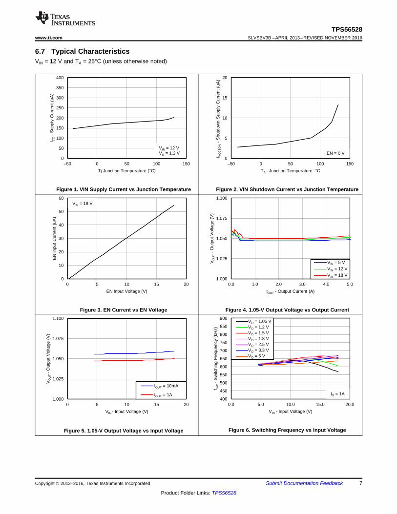
6.7 Typical CharacteristicsVIN = 12 V and TA = 25°C (unless otherwise noted)
Figure 1. VIN Supply Current vs Junction Temperature Figure 2. VIN Shutdown Current vs Junction Temperature
Figure 3. EN Current vs EN Voltage Figure 4. 1.05-V Output Voltage vs Output Current
Figure 5. 1.05-V Output Voltage vs Input Voltage Figure 6. Switching Frequency vs Input Voltage

0.00
1.00
2.00
3.00
4.00
5.00
6.00
0 20 40 60 80 100
V = 1.0 to 4.5VO
V = 5VO
V = 6VO
V = 7VO
Outp
ut
Curr
ent
(A)
Ambient Temperature (°C)
0.585
0.590
0.595
0.600
0.605
0.610
0.615
-50 0 50 100 150
VF
B V
olta
ge -
V
TJ - Junction Temperature - �C
Iout = 1 A
C015
0
100
200
300
400
500
600
700
800
0 1 2 3 4 5
f SW
- S
witc
hing
Fre
quen
cy (
kHz)
IOUT - Output Current (A)
VIN=5V
VIN=12V
VIN=18V
C012
VO = 1.05 V VO = 1.8 V
VO = 3.3 V
8
TPS56528SLVSBV3B –APRIL 2013–REVISED NOVEMBER 2016 www.ti.com
Product Folder Links: TPS56528
Submit Documentation Feedback Copyright © 2013–2016, Texas Instruments Incorporated
Typical Characteristics (continued)VIN = 12 V and TA = 25°C (unless otherwise noted)
Figure 7. Switching Frequency vs Output Current Figure 8. VFB Voltage vs Junction Temperature
Figure 9. Output Current vs Ambient Temperature
SW
VBST
EN
VFB
GND
VO
5
6
4
7
VIN
PG
VIN
VREG5
ENLogic
SW
OCL
ProtectionLogic
REF
SS
UVLO
UVLO
Softstart SS
REF
TSD
REF
VREG5
8
VIN
CeramicCapacitor
3AGND
PGND
PWM+
-
+
OCP
+
-
VREG5
XCON
VREG5
Control Logic
1 shot
ON
SW
PGNDZC
+
-
2
1
OV
+
-
+
-
+25%OV
EN
REF
-10%
EN
PGND
Copyright © 2016, Texas Instruments Incorporated
9
TPS56528www.ti.com SLVSBV3B –APRIL 2013–REVISED NOVEMBER 2016
Product Folder Links: TPS56528
Submit Documentation FeedbackCopyright © 2013–2016, Texas Instruments Incorporated
7 Detailed Description
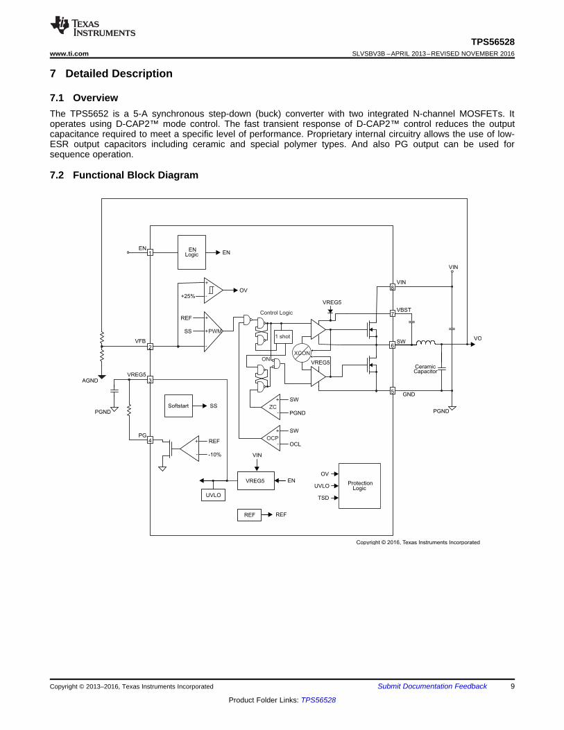
7.1 OverviewThe TPS5652 is a 5-A synchronous step-down (buck) converter with two integrated N-channel MOSFETs. Itoperates using D-CAP2™ mode control. The fast transient response of D-CAP2™ control reduces the outputcapacitance required to meet a specific level of performance. Proprietary internal circuitry allows the use of low-ESR output capacitors including ceramic and special polymer types. And also PG output can be used forsequence operation.
7.2 Functional Block Diagram
10
TPS56528SLVSBV3B –APRIL 2013–REVISED NOVEMBER 2016 www.ti.com
Product Folder Links: TPS56528
Submit Documentation Feedback Copyright © 2013–2016, Texas Instruments Incorporated
7.3 Feature Description
7.3.1 PWM OperationThe main control loop of the TPS56528 is an adaptive on-time pulse width modulation (PWM) controller thatsupports a proprietary D-CAP2™ mode control. D-CAP2™ mode control combines constant on-time control withan internal compensation circuit for pseudo-fixed frequency and low external component count configuration withboth low-ESR and ceramic output capacitors. It is stable even with virtually no ripple at the output.
At the beginning of each cycle, the high-side MOSFET is turned on. This MOSFET is turned off after internalone-shot timer expires. This one shot is set by the converter input voltage, VIN, and the output voltage, VO, tomaintain a pseudo-fixed frequency over the input voltage range, hence it is called adaptive on-time control. Theone-shot timer is reset and the high-side MOSFET is turned on again when the feedback voltage falls below thereference voltage. An internal ramp is added to reference voltage to simulate output ripple, eliminating therequirement for ESR-induced output ripple from D-CAP2™ mode control.
7.3.2 PWM Frequency and Adaptive On-Time ControlTPS56528 uses an adaptive on-time control scheme and does not have a dedicated on board oscillator. TheTPS56528 runs with a pseudo-constant frequency of 650 kHz by using the input voltage and output voltage toset the on-time one-shot timer. The on-time is inversely proportional to the input voltage and proportional to theoutput voltage; therefore, when the duty ratio is VOUT/VIN, the frequency is constant.
7.3.3 Soft Start and Prebiased Soft StartThe TPS56528 has an internal 1-ms soft start. When the EN pin becomes high, internal soft-start function beginsramping up the reference voltage to the PWM comparator.
The TPS56528 contains a unique circuit to prevent current from being pulled from the output during start-up if theoutput is prebiased. When the soft start commands a voltage higher than the prebias level (internal soft startbecomes greater than feedback voltage VFB), the controller slowly activates synchronous rectification by startingthe first low-side FET gate driver pulses with a narrow on-time. It then increments that on-time on a cycle-by-cycle basis until it coincides with the time dictated by (1-D), where D is the duty cycle of the converter. Thisscheme prevents the initial sinking of the prebias output, and ensure that the out voltage (VO) starts and rampsup smoothly into regulation and the control loop is given time to transition from prebiased start-up to normalmode operation.
7.3.4 Power GoodThe power good function is activated after soft start has finished. The power good function becomes active after1.7 × soft-start time. When the output voltage becomes within –10% of the target value, internal comparatorsdetect power good state and the power good signal becomes high. The power good output, PG is an open-drainoutput. If the feedback voltage goes under 15% of the target value, the power good signal becomes low.
7.3.5 Output Discharge ControlTPS56528 discharges the output through the SW pin when EN is low, or the controller is turned off by theprotection functions (UVP, UVLO and thermal shutdown). The internal regular low-side MOSFET is not turned onduring the output discharge operation to avoid the possibility of causing negative voltage at the output.
7.3.6 Current ProtectionThe output overcurrent protection (OCP) is implemented using a cycle-by-cycle valley detect control circuit. Theswitch current is monitored by measuring the low-side FET switch voltage between the SW pin and GND. Thisvoltage is proportional to the switch current. To improve accuracy, the voltage sensing is temperaturecompensated.
During the on-time of the high-side FET switch, the switch current increases at a linear rate determined by VIN,VOUT, the on-time and the output inductor value. During the on-time of the low-side FET switch, this currentdecreases linearly. The average value of the switch current is the load current, Iout. The TPS56528 constantlymonitors the low-side FET switch voltage, which is proportional to the switch current, during the low-side on-time.If the measured voltage is above the voltage proportional to the current limit, an internal counter is incrementedper each SW cycle and the converter maintains the low-side switch on until the measured voltage is below thevoltage corresponding to the current limit at which time the switching cycle is terminated and a new switching
( )( )
2
IN OUT OUTOUT LL
IN
V V VI
L fsw V
- ×= ×
× ×
1
11
TPS56528www.ti.com SLVSBV3B –APRIL 2013–REVISED NOVEMBER 2016
Product Folder Links: TPS56528
Submit Documentation FeedbackCopyright © 2013–2016, Texas Instruments Incorporated
Feature Description (continued)cycle begins. In subsequent switching cycles, the on-time is set to a fixed value and the current is monitored inthe same manner. If the over current condition exists for 7 consecutive switching cycles, the internal OCLthreshold is set to a lower level, reducing the available output current. When a switching cycle occurs where theswitch current is not above the lower OCL threshold, the counter is reset and the OCL limit is returned to thehigher value.
There are some important considerations for this type of overcurrent protection. The peak current is the averageload current plus one half of the peak-to-peak inductor current. The valley current is the average load currentminus one half of the peak-to-peak inductor current. Because the valley current is used to detect the overcurrentthreshold, the load current is higher than the overcurrent threshold. Also, when the current is being limited, theoutput voltage tends to fall as the demanded load current may be higher than the current available from theconverter. This protection is non-latching. When the VFB voltage becomes lower than 65% of the target voltage,the UVP comparator detects it. After 7 µs detecting the UVP voltage, device shut downs and restarts after hiccuptime.
When the overcurrent condition is removed, the output voltage returns to the regulated value.
7.3.7 UVLO ProtectionUndervoltage lockout protection (UVLO) monitors the voltage of the VREG5 pin. When the VREG5 voltage is lowerthan UVLO threshold voltage, the TPS56528 is shut off. This protection is non-latching.
7.3.8 Thermal ShutdownTPS56528 monitors the temperature of itself. If the temperature exceeds the threshold value (typically 165°C),the device is shut off. This is non-latch protection.
7.4 Device Functional Modes
7.4.1 Advanced Auto-Skip Eco-Mode™ ControlThe TPS56528 is designed with advanced auto-skip Eco-Mode™ to increase higher light load efficiency. As theoutput current decreases from heavy load condition, the inductor current is also reduced. If the output current isreduced enough, the inductor current ripple valley reaches the zero level, which is the boundary betweencontinuous conduction and discontinuous conduction modes. The rectifying low-side MOSFET is turned off whenits zero inductor current is detected. As the load current further decreases the converter run into discontinuousconduction mode. The on-time is kept approximately the same as is in continuous conduction mode. The off-timeincreases as it takes more time to discharge the output capacitor to the level of the reference voltage withsmaller load current. The transition point to the light load operation IOUT(LL) current can be calculated inEquation 1.
(1)
U1TPS56528DDA
Copyright © 2016, Texas Instruments Incorporated
12
TPS56528SLVSBV3B –APRIL 2013–REVISED NOVEMBER 2016 www.ti.com
Product Folder Links: TPS56528
Submit Documentation Feedback Copyright © 2013–2016, Texas Instruments Incorporated
8 Application and Implementation
NOTEInformation in the following applications sections is not part of the TI componentspecification, and TI does not warrant its accuracy or completeness. TI’s customers areresponsible for determining suitability of components for their purposes. Customers shouldvalidate and test their design implementation to confirm system functionality.
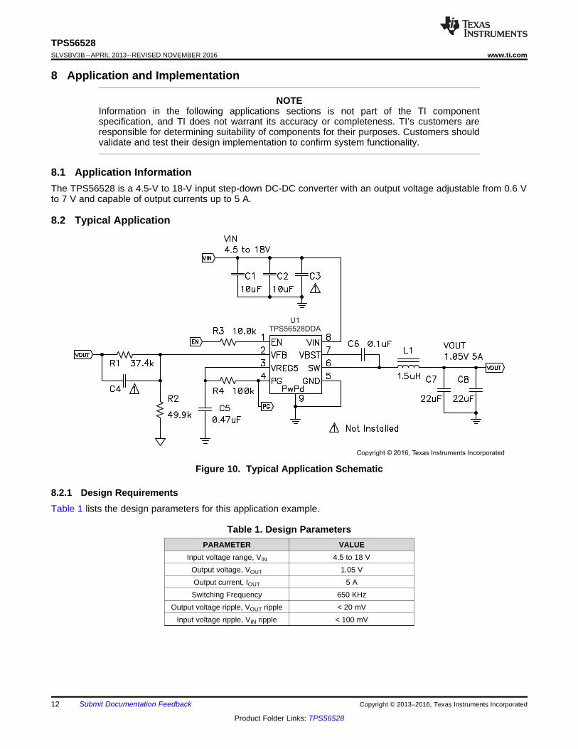
8.1 Application InformationThe TPS56528 is a 4.5-V to 18-V input step-down DC-DC converter with an output voltage adjustable from 0.6 Vto 7 V and capable of output currents up to 5 A.
8.2 Typical Application
Figure 10. Typical Application Schematic
8.2.1 Design RequirementsTable 1 lists the design parameters for this application example.
Table 1. Design ParametersPARAMETER VALUE
Input voltage range, VIN 4.5 to 18 VOutput voltage, VOUT 1.05 VOutput current, IOUT 5 ASwitching Frequency 650 KHz
Output voltage ripple, VOUT ripple < 20 mVInput voltage ripple, VIN ripple < 100 mV

P PPEAK O
ll I
2
-= +
II
IN(MAX) OUTOUTP P
IN(MAX) O SW
V VVl
V L-
-= ´
´ ¦I
P
OUT OUT
1F
2 L C=
p ´
OUT
R1V 0.60 1
R2
æ ö= ´ +ç ÷
è ø
13
TPS56528www.ti.com SLVSBV3B –APRIL 2013–REVISED NOVEMBER 2016
Product Folder Links: TPS56528
Submit Documentation FeedbackCopyright © 2013–2016, Texas Instruments Incorporated
(1) Optional
8.2.2 Detailed Design Procedure
8.2.2.1 Output Voltage Resistors SelectionThe output voltage is set with a resistor divider from the output node to the VFB pin. TI recommends using 1%tolerance or better divider resistors. Start by using Equation 2 to calculate VOUT.
To improve efficiency at light loads, consider using larger value resistors, high resistance is more susceptible tonoise, and the voltage errors from the VFB input current are more noticeable.
(2)
8.2.2.2 Output Filter SelectionThe output filter used with the TPS56528 is an LC circuit. This LC filter has double pole in Equation 3.
(3)
At low frequencies, the overall loop gain is set by the output setpoint resistor divider network and the internalgain of the TPS56528. The low frequency phase is 180 degrees. At the output filter pole frequency, the gain rollsoff at a –40 dB per decade rate and the phase drops rapidly. D-CAP2™ introduces a high frequency zero thatreduces the gain roll off to –20 dB per decade and increases the phase to 90 degrees one decade above thezero frequency. The inductor and capacitor selected for the output filter must be selected so that the double poleof Equation 3 is located below the high frequency zero but close enough that the phase boost provided by thehigh frequency zero provides adequate phase margin for a stable circuit. To meet this requirement, use thevalues recommended in Table 2.
Table 2. Recommended Component ValuesOUTPUT
VOLTAGE(V)
R1 (kΩ) R2 (kΩ)C4 (pF) (1) L1 (µH) C7 + C8
(µF)MIN TYP MAX MIN TYP MAX
1 33.2 49.9 5 33 100 1 1.5 4.7 20 to 681.05 37.4 49.9 5 33 100 1 1.5 4.7 20 to 681.2 49.9 49.9 5 22 47 1 1.5 4.7 20 to 681.5 75.0 49.9 5 15 33 1 1.5 4.7 20 to 681.8 100 49.9 5 10 22 1 1.5 4.7 20 to 682.5 158 49.9 5 10 22 1.5 2.2 4.7 20 to 683.3 226 49.9 2 5 15 1.5 2.2 4.7 20 to 685 365 49.9 2 5 10 2.2 3.3 4.7 20 to 68
6.5 487 49.9 2 2 10 2.2 3.3 4.7 20 to 68
For higher output voltages at or above 1.8 V, additional phase boost can be achieved by adding a feed-forwardcapacitor (C4) in parallel with R1
The inductor peak-to-peak ripple current, peak current, and RMS current are calculated using Equation 4,Equation 5, and Equation 6. The inductor saturation current rating must be greater than the calculated peakcurrent and the RMS or heating current rating must be greater than the calculated RMS current. Use 650 kHz forfSW.
Ensure the chosen inductor is rated for the peak current of Equation 5 and the RMS current of Equation 6.
(4)
(5)
Vout( 50mV/div)
Iout( 2A/div)
100us/div
Vout( 0.5V/div)
EN( 10V/div)
400us/div
VREG5( 5V/div)
PG( 5V/div)
INOUT OUT=Co(RMS)
IN O SW
V x (V - V )
12 x V x L xI
f
2 2LO(RMS) O P P
1I I l
12-
= + I
14
TPS56528SLVSBV3B –APRIL 2013–REVISED NOVEMBER 2016 www.ti.com
Product Folder Links: TPS56528
Submit Documentation Feedback Copyright © 2013–2016, Texas Instruments Incorporated
(6)
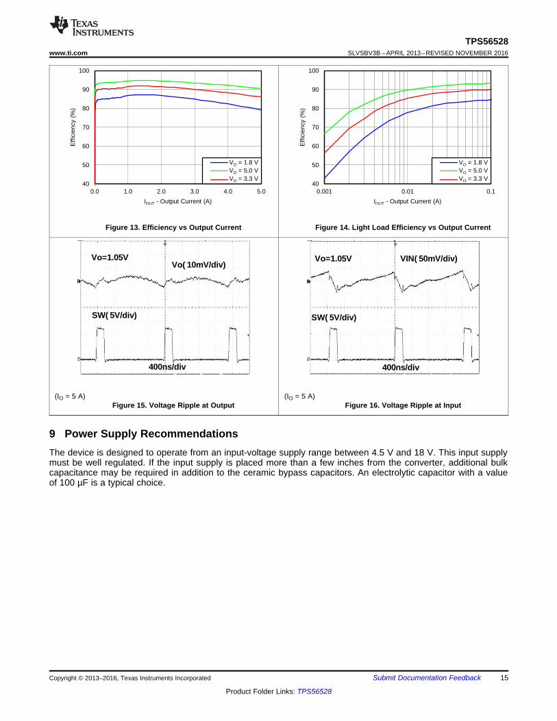
For this design example, the calculated peak current is 5.51 A and the calculated RMS current is 5.01 A.The inductor used is a TDK SPM6530-1R5M100 with a peak current rating of 11.5 A and an RMS current ratingof 11 A.
The capacitor value and ESR determines the amount of output voltage ripple. The TPS56528 is intended for usewith ceramic or other low-ESR capacitors. Recommended values range from 20 µF to 68 µF. Use Equation 7 todetermine the required RMS current rating for the output capacitor.
(7)
For this design, two TDK C3216X5R0J226M 22-µF output capacitors are used. The typical ESR is 2 mΩ each.The calculated RMS current is 0.284 A and each output capacitor is rated for 4 A.
8.2.2.3 Input Capacitor SelectionThe TPS56528 requires an input decoupling capacitor and a bulk capacitor is required depending on theapplication. A ceramic capacitor over 10 μF is recommended for the decoupling capacitor. An additional 0.1-µFcapacitor (C3) from pin 8 to ground is optional to provide additional high frequency filtering. The capacitor voltagerating requires greater than the maximum input voltage.
8.2.2.4 Bootstrap Capacitor SelectionA 0.1-µF ceramic capacitor must be connected between the VBST to SW pin for proper operation. TIrecommends using a ceramic capacitor.
8.2.2.5 VREG5 Capacitor SelectionA 0.47-µF ceramic capacitor must be connected between the VREG5 to GND pin for proper operation. TIrecommends using a ceramic capacitor.
8.2.3 Application Curves
Figure 11. 1.05-V, Load Transient Response Figure 12. Start-Up Waveform
SW( 5V/div)
Vo=1.05VVo( 10mV/div)
400ns/div
Vo=1.05V VIN( 50mV/div)
SW( 5V/div)
400ns/div
40
50
60
70
80
90
100
0.0 1.0 2.0 3.0 4.0 5.0
Effi
cien
cy (
%)
IOUT - Output Current (A)
Vo=1.8V Vo = 5 V Vo=3.3V
C008
VO = 1.8 V VO = 5.0 V VO = 3.3 V
40
50
60
70
80
90
100
0.001 0.01 0.1
Effi
cien
cy (
%)
IOUT - Output Current (A)
Vo=1.8V Vo = 5 V Vo=3.3V
C009
VO = 1.8 V VO = 5.0 V VO = 3.3 V
15
TPS56528www.ti.com SLVSBV3B –APRIL 2013–REVISED NOVEMBER 2016
Product Folder Links: TPS56528
Submit Documentation FeedbackCopyright © 2013–2016, Texas Instruments Incorporated
Figure 13. Efficiency vs Output Current Figure 14. Light Load Efficiency vs Output Current
(IO = 5 A)Figure 15. Voltage Ripple at Output
(IO = 5 A)Figure 16. Voltage Ripple at Input
9 Power Supply RecommendationsThe device is designed to operate from an input-voltage supply range between 4.5 V and 18 V. This input supplymust be well regulated. If the input supply is placed more than a few inches from the converter, additional bulkcapacitance may be required in addition to the ceramic bypass capacitors. An electrolytic capacitor with a valueof 100 µF is a typical choice.
VFB
VREG5
PG GND
EN VIN
VBST
SW
EXPOSED
THERMAL PAD
AREA
BOOST
CAPACITOR
VOUT
VIA to Ground Plane
OUTPUT
INDUCTOR
OUTPUT
FILTER
CAPACITOR
POWER
GOOD
PULL UP
ANALOG
GROUND
TRACE
VIN
INPUT
BYPASS
CAPACITOR
VIN
FEEDBACK
RESISTORS
TO ENABLE
CONTROL
POWER GROUND
BIAS
CAP
VIN
HIGH FREQENCY
BYPASS
CAPACITOR
TO POWER
GOOD
MONITOR
16
TPS56528SLVSBV3B –APRIL 2013–REVISED NOVEMBER 2016 www.ti.com
Product Folder Links: TPS56528
Submit Documentation Feedback Copyright © 2013–2016, Texas Instruments Incorporated
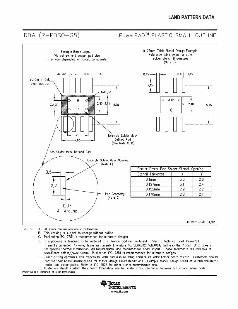
10 Layout
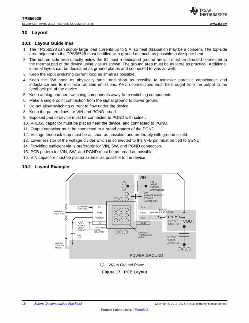
10.1 Layout Guidelines1. The TPS56528 can supply large load currents up to 5 A, so heat dissipation may be a concern. The top-side
area adjacent to the TPS56528 must be filled with ground as much as possible to dissipate heat.2. The bottom side area directly below the IC must a dedicated ground area. It must be directed connected to
the thermal pad of the device using vias as shown. The ground area must be as large as practical. Additionalinternal layers can be dedicated as ground planes and connected to vias as well.
3. Keep the input switching current loop as small as possible.4. Keep the SW node as physically small and short as possible to minimize parasitic capacitance and
inductance and to minimize radiated emissions. Kelvin connections must be brought from the output to thefeedback pin of the device.
5. Keep analog and non-switching components away from switching components.6. Make a single point connection from the signal ground to power ground.7. Do not allow switching current to flow under the device.8. Keep the pattern lines for VIN and PGND broad.9. Exposed pad of device must be connected to PGND with solder.10. VREG5 capacitor must be placed near the device, and connected to PGND.11. Output capacitor must be connected to a broad pattern of the PGND.12. Voltage feedback loop must be as short as possible, and preferably with ground shield.13. Lower resistor of the voltage divider which is connected to the VFB pin must be tied to SGND.14. Providing sufficient via is preferable for VIN, SW, and PGND connection.15. PCB pattern for VIN, SW, and PGND must be as broad as possible.16. VIN capacitor must be placed as near as possible to the device.
10.2 Layout Example
Figure 17. PCB Layout
17
TPS56528www.ti.com SLVSBV3B –APRIL 2013–REVISED NOVEMBER 2016
Product Folder Links: TPS56528
Submit Documentation FeedbackCopyright © 2013–2016, Texas Instruments Incorporated
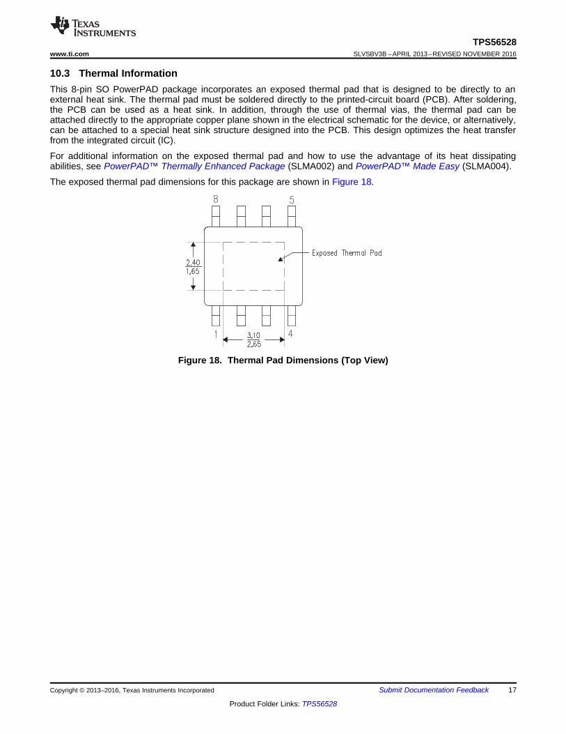
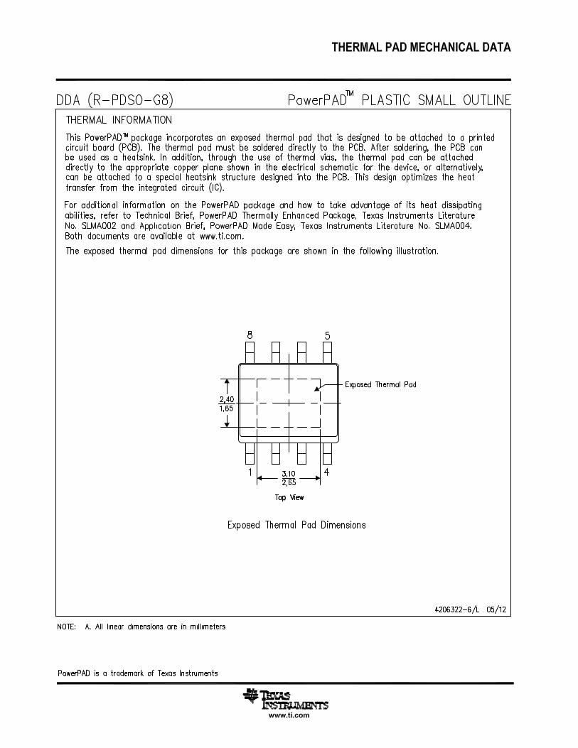
10.3 Thermal InformationThis 8-pin SO PowerPAD package incorporates an exposed thermal pad that is designed to be directly to anexternal heat sink. The thermal pad must be soldered directly to the printed-circuit board (PCB). After soldering,the PCB can be used as a heat sink. In addition, through the use of thermal vias, the thermal pad can beattached directly to the appropriate copper plane shown in the electrical schematic for the device, or alternatively,can be attached to a special heat sink structure designed into the PCB. This design optimizes the heat transferfrom the integrated circuit (IC).
For additional information on the exposed thermal pad and how to use the advantage of its heat dissipatingabilities, see PowerPAD™ Thermally Enhanced Package (SLMA002) and PowerPAD™ Made Easy (SLMA004).
The exposed thermal pad dimensions for this package are shown in Figure 18.
Figure 18. Thermal Pad Dimensions (Top View)
18
TPS56528SLVSBV3B –APRIL 2013–REVISED NOVEMBER 2016 www.ti.com
Product Folder Links: TPS56528
Submit Documentation Feedback Copyright © 2013–2016, Texas Instruments Incorporated
11 Device and Documentation Support
11.1 Device Support
11.1.1 Third-Party Products DisclaimerTI'S PUBLICATION OF INFORMATION REGARDING THIRD-PARTY PRODUCTS OR SERVICES DOES NOTCONSTITUTE AN ENDORSEMENT REGARDING THE SUITABILITY OF SUCH PRODUCTS OR SERVICESOR A WARRANTY, REPRESENTATION OR ENDORSEMENT OF SUCH PRODUCTS OR SERVICES, EITHERALONE OR IN COMBINATION WITH ANY TI PRODUCT OR SERVICE.
11.2 Documentation Support
11.2.1 Related DocumentationFor related documentation see the following:• PowerPAD™ Thermally Enhanced Package (SLMA002)• PowerPAD™ Made Easy (SLMA004)
11.3 Receiving Notification of Documentation UpdatesTo receive notification of documentation updates, navigate to the device product folder on ti.com. In the upperright corner, click on Alert me to register and receive a weekly digest of any product information that haschanged. For change details, review the revision history included in any revised document.
11.4 Community ResourcesThe following links connect to TI community resources. Linked contents are provided "AS IS" by the respectivecontributors. They do not constitute TI specifications and do not necessarily reflect TI's views; see TI's Terms ofUse.
TI E2E™ Online Community TI's Engineer-to-Engineer (E2E) Community. Created to foster collaborationamong engineers. At e2e.ti.com, you can ask questions, share knowledge, explore ideas and helpsolve problems with fellow engineers.
Design Support TI's Design Support Quickly find helpful E2E forums along with design support tools andcontact information for technical support.
11.5 TrademarksD-CAP2, Eco-Mode, PowerPAD, E2E are trademarks of Texas Instruments.Blu-ray Disc is a trademark of Blu-ray Disc Association.All other trademarks are the property of their respective owners.
11.6 Electrostatic Discharge CautionThese devices have limited built-in ESD protection. The leads should be shorted together or the device placed in conductive foamduring storage or handling to prevent electrostatic damage to the MOS gates.
11.7 GlossarySLYZ022 — TI Glossary.
This glossary lists and explains terms, acronyms, and definitions.
12 Mechanical, Packaging, and Orderable InformationThe following pages include mechanical, packaging, and orderable information. This information is the mostcurrent data available for the designated devices. This data is subject to change without notice and revision ofthis document. For browser-based versions of this data sheet, refer to the left-hand navigation.
PACKAGE OPTION ADDENDUM
www.ti.com 10-Dec-2020
Addendum-Page 1
PACKAGING INFORMATION
Orderable Device Status(1)
Package Type PackageDrawing
Pins PackageQty
Eco Plan(2)
Lead finish/Ball material
(6)
MSL Peak Temp(3)
Op Temp (°C) Device Marking(4/5)
Samples
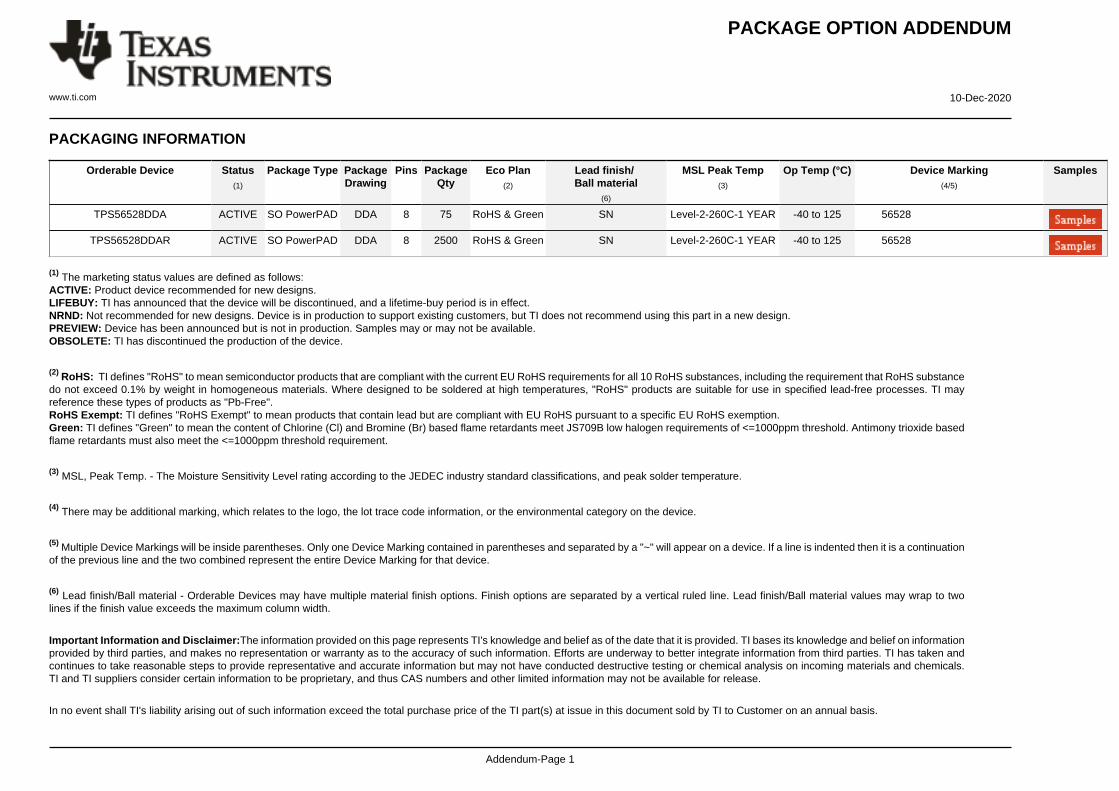
TPS56528DDA ACTIVE SO PowerPAD DDA 8 75 RoHS & Green SN Level-2-260C-1 YEAR -40 to 125 56528
TPS56528DDAR ACTIVE SO PowerPAD DDA 8 2500 RoHS & Green SN Level-2-260C-1 YEAR -40 to 125 56528
(1) The marketing status values are defined as follows:ACTIVE: Product device recommended for new designs.LIFEBUY: TI has announced that the device will be discontinued, and a lifetime-buy period is in effect.NRND: Not recommended for new designs. Device is in production to support existing customers, but TI does not recommend using this part in a new design.PREVIEW: Device has been announced but is not in production. Samples may or may not be available.OBSOLETE: TI has discontinued the production of the device.
(2) RoHS: TI defines "RoHS" to mean semiconductor products that are compliant with the current EU RoHS requirements for all 10 RoHS substances, including the requirement that RoHS substancedo not exceed 0.1% by weight in homogeneous materials. Where designed to be soldered at high temperatures, "RoHS" products are suitable for use in specified lead-free processes. TI mayreference these types of products as "Pb-Free".RoHS Exempt: TI defines "RoHS Exempt" to mean products that contain lead but are compliant with EU RoHS pursuant to a specific EU RoHS exemption.Green: TI defines "Green" to mean the content of Chlorine (Cl) and Bromine (Br) based flame retardants meet JS709B low halogen requirements of <=1000ppm threshold. Antimony trioxide basedflame retardants must also meet the <=1000ppm threshold requirement.
(3) MSL, Peak Temp. - The Moisture Sensitivity Level rating according to the JEDEC industry standard classifications, and peak solder temperature.
(4) There may be additional marking, which relates to the logo, the lot trace code information, or the environmental category on the device.
(5) Multiple Device Markings will be inside parentheses. Only one Device Marking contained in parentheses and separated by a "~" will appear on a device. If a line is indented then it is a continuationof the previous line and the two combined represent the entire Device Marking for that device.
(6) Lead finish/Ball material - Orderable Devices may have multiple material finish options. Finish options are separated by a vertical ruled line. Lead finish/Ball material values may wrap to twolines if the finish value exceeds the maximum column width.
Important Information and Disclaimer:The information provided on this page represents TI's knowledge and belief as of the date that it is provided. TI bases its knowledge and belief on informationprovided by third parties, and makes no representation or warranty as to the accuracy of such information. Efforts are underway to better integrate information from third parties. TI has taken andcontinues to take reasonable steps to provide representative and accurate information but may not have conducted destructive testing or chemical analysis on incoming materials and chemicals.TI and TI suppliers consider certain information to be proprietary, and thus CAS numbers and other limited information may not be available for release.
In no event shall TI's liability arising out of such information exceed the total purchase price of the TI part(s) at issue in this document sold by TI to Customer on an annual basis.

PACKAGE OPTION ADDENDUM
www.ti.com 10-Dec-2020
Addendum-Page 2
TAPE AND REEL INFORMATION
*All dimensions are nominal
Device PackageType
PackageDrawing
Pins SPQ ReelDiameter
(mm)
ReelWidth
W1 (mm)
A0(mm)
B0(mm)
K0(mm)
P1(mm)
W(mm)
Pin1Quadrant
TPS56528DDAR SOPower PAD
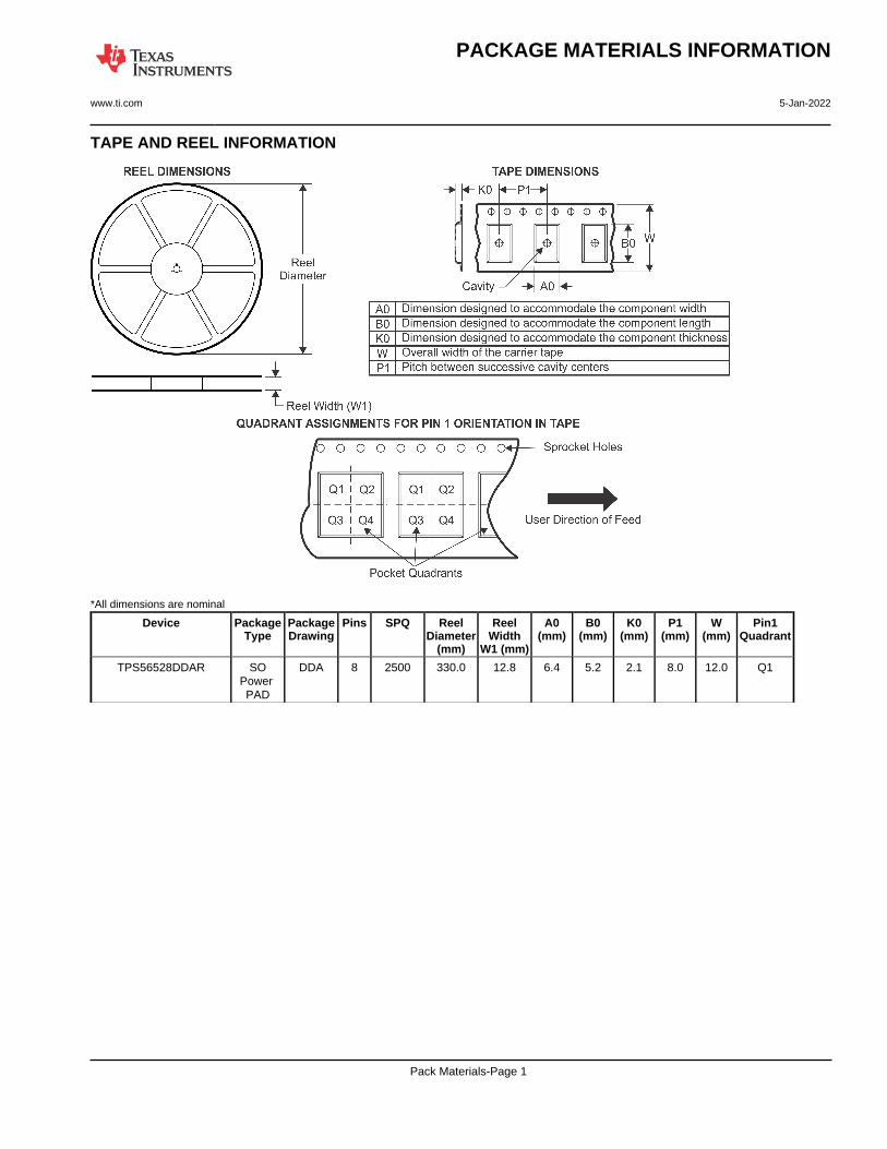
DDA 8 2500 330.0 12.8 6.4 5.2 2.1 8.0 12.0 Q1
PACKAGE MATERIALS INFORMATION
www.ti.com 5-Jan-2022
Pack Materials-Page 1
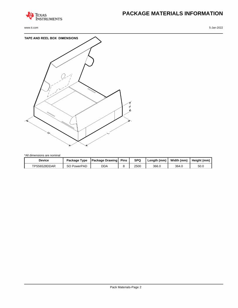
*All dimensions are nominal
Device Package Type Package Drawing Pins SPQ Length (mm) Width (mm) Height (mm)
TPS56528DDAR SO PowerPAD DDA 8 2500 366.0 364.0 50.0
PACKAGE MATERIALS INFORMATION
www.ti.com 5-Jan-2022
Pack Materials-Page 2

TUBE
*All dimensions are nominal
Device Package Name Package Type Pins SPQ L (mm) W (mm) T (µm) B (mm)
TPS56528DDA DDA HSOIC 8 75 517 7.87 635 4.25
PACKAGE MATERIALS INFORMATION
www.ti.com 5-Jan-2022
Pack Materials-Page 3

GENERIC PACKAGE VIEW
Images above are just a representation of the package family, actual package may vary.Refer to the product data sheet for package details.
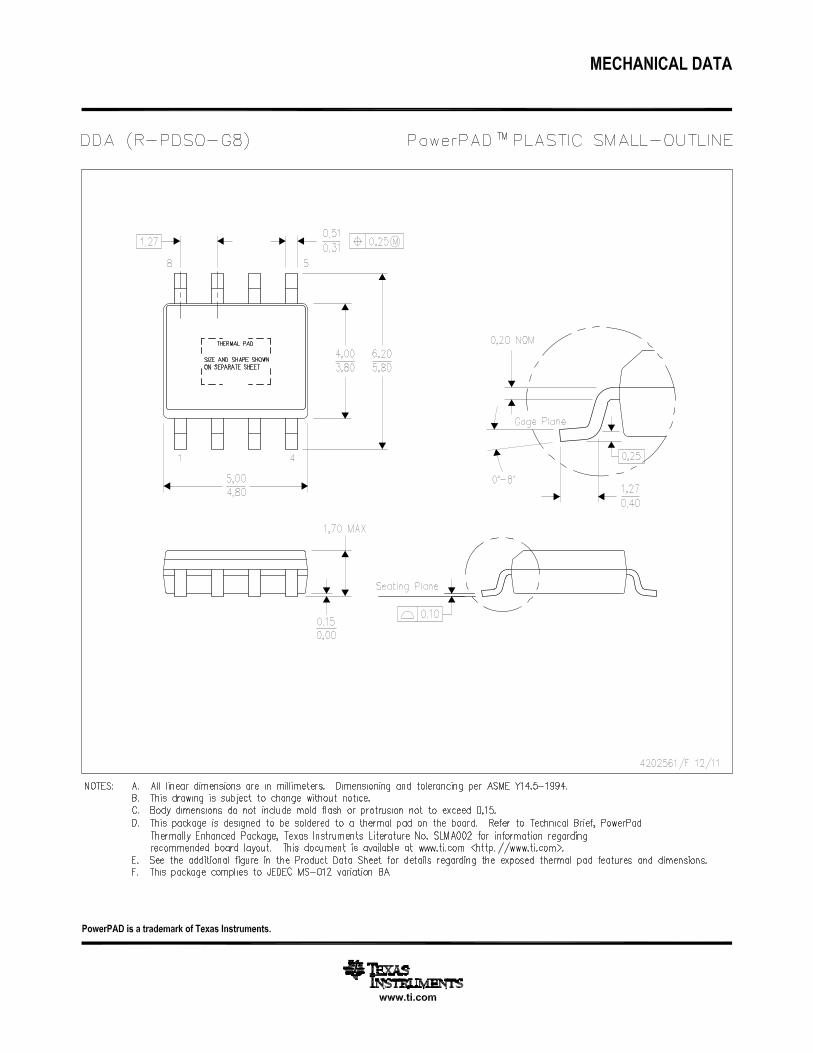
DDA 8 PowerPAD TM SOIC - 1.7 mm max heightPLASTIC SMALL OUTLINE
4202561/G

IMPORTANT NOTICE AND DISCLAIMERTI PROVIDES TECHNICAL AND RELIABILITY DATA (INCLUDING DATA SHEETS), DESIGN RESOURCES (INCLUDING REFERENCE DESIGNS), APPLICATION OR OTHER DESIGN ADVICE, WEB TOOLS, SAFETY INFORMATION, AND OTHER RESOURCES “AS IS” AND WITH ALL FAULTS, AND DISCLAIMS ALL WARRANTIES, EXPRESS AND IMPLIED, INCLUDING WITHOUT LIMITATION ANY IMPLIED WARRANTIES OF MERCHANTABILITY, FITNESS FOR A PARTICULAR PURPOSE OR NON-INFRINGEMENT OF THIRD PARTY INTELLECTUAL PROPERTY RIGHTS.These resources are intended for skilled developers designing with TI products. You are solely responsible for (1) selecting the appropriate TI products for your application, (2) designing, validating and testing your application, and (3) ensuring your application meets applicable standards, and any other safety, security, regulatory or other requirements.These resources are subject to change without notice. TI grants you permission to use these resources only for development of an application that uses the TI products described in the resource. Other reproduction and display of these resources is prohibited. No license is granted to any other TI intellectual property right or to any third party intellectual property right. TI disclaims responsibility for, and you will fully indemnify TI and its representatives against, any claims, damages, costs, losses, and liabilities arising out of your use of these resources.TI’s products are provided subject to TI’s Terms of Sale or other applicable terms available either on ti.com or provided in conjunction with such TI products. TI’s provision of these resources does not expand or otherwise alter TI’s applicable warranties or warranty disclaimers for TI products.TI objects to and rejects any additional or different terms you may have proposed. IMPORTANT NOTICE
Mailing Address: Texas Instruments, Post Office Box 655303, Dallas, Texas 75265Copyright © 2022, Texas Instruments Incorporated