tpel.2013.2294425
DESCRIPTION
paperTRANSCRIPT

Copyright (c) 2013 IEEE. Personal use is permitted. For any other purposes, permission must be obtained from the IEEE by emailing [email protected].
This article has been accepted for publication in a future issue of this journal, but has not been fully edited. Content may change prior to final publication. Citation information: DOI10.1109/TPEL.2013.2294425, IEEE Transactions on Power Electronics
1
Control of Inverters via a Virtual Capacitor to
Achieve Capacitive Output ImpedanceQing-Chang Zhong,Senior Member, IEEE,and Yu Zeng
Abstract
Mainstream inverters have inductive output impedance at low frequencies (such inverters are called L-inverters). In this paper,
a control strategy is proposed to make the output impedance of an inverter capacitive at low frequencies (such invertersare called
C-inverters). The proposed control strategy involves the feedback of the inductor current through an integrator, which is actually
the impedance of a virtual capacitor. The gain of the integrator or the virtual capacitance is firstly selected to guarantee the stability
of the current feedback loop and then optimised to minimise the total harmonic distortion (THD) of the output voltage. Moreover,
some guidelines are developed to facilitate the selection of the filter components for C-inverters. Simulation and experimental
results are provided to demonstrate the feasibility and excellent performance of C-inverters, with the filter parameters of the test
rig selected according to the guidelines developed. It is shown that, with the same hardware, the lowest voltage THD is obtained
when the inverter is designed to be a C-inverter. A by-product of this study is that, as long as the current ripples are keptwithin
the desired range, the filter inductor should be chosen as small as possible in order to reduce voltage harmonics. This helps reduce
the size, weight and volume of the inductor and improve the power density of the inverter.
Index Terms
Power quality, total harmonic distortion (THD), inverterswith capacitive output impedance (C-inverters), inverters with
inductive output impedance (L-inverters), inverters withresistive output impedance (R-inverters)
I. I NTRODUCTION
Energy and sustainability are now on the top agenda of many governments. Smart grids have become one of the main
enablers to address energy and sustainability issues. Renewable energy, distributed generation, hybrid electrical vehicles, more-
electric aircraft, all-electric ships, smart grids etc. will become more and more popular. DC/AC converters, also called inverters,
play a common role in these applications to convert a DC source into an AC source. Arguably, the integration of renewable
and distributed energy sources, energy storage and demand-side resources into smart grids is the largest “new frontier” for
smart grid advancements [1], [2]. Inverters are also widelyused in uninterruptible power supplies (UPS), induction heating,
high-voltage DC (HVDC) transmission, variable-frequencydrives, electric vehicle (EV) drives, air conditioning, vehicle-to-grid
Some preliminary results were presented at the 37th Annual Conference of the IEEE Industrial Electronics Society (IECON), Melbourne, Australia, November2011.
Qing-Chang Zhong and Yu Zeng are with the Dept. of Automatic Control and Systems Engineering, The University of Sheffield, Sheffield,S1 3JD, UK, email: [email protected]; [email protected], tel: +44-114 22 25630, fax: +44-114 22 25683.
The financial support from the EPSRC, UK under Grant No. EP/J001333/1 and EP/J01558X/1 is greatly appreciated.

Copyright (c) 2013 IEEE. Personal use is permitted. For any other purposes, permission must be obtained from the IEEE by emailing [email protected].
This article has been accepted for publication in a future issue of this journal, but has not been fully edited. Content may change prior to final publication. Citation information: DOI10.1109/TPEL.2013.2294425, IEEE Transactions on Power Electronics
2
(V2G) etc. and, hence, have become a common key device for many energy-related applications. How to control inverters is
critical for these applications.
There are several important control problems associated with inverters. For example, how to make sure that the total harmonic
distortion (THD) of the inverter voltage remains within certain range when the loads are nonlinear and the grid voltage,if
present, is distorted; how to make sure that the output voltage of an inverter is maintained within a certain range; how to
share loads proportionally according to their power ratings when inverters are operated in parallel; how to make sure that
inverters can be operated in the grid-connected mode and thestandalone mode and how to minimise the transient dynamics
when the operation mode is changed [3]; how to connect inverters to the grid in a grid-friendly manner so that the impact on
the grid is minimised [4], [5]; how to minimizing the total microgrid operating cost [6], etc. There have been a lot of research
activities on these problems, from one aspect to another, and a systematic treatment of the control problems related to inverters
in renewable energy and smart grid integration can be found in [1].
The voltage THD can be improved by using deadbeat or hysteresis controllers [7], [8], selective harmonic elimination
pulsewidth modulation strategies [9], and repetitive controllers [10]–[16] [17], [18], injecting harmonic voltages[19], [20],
introducing a voltage feedback loop [21] etc. Another way isto investigate the role of the output impedance as it is known
that the output filter also contributes to the output voltagequality [22]–[25]. It is well known that mainstream inverters have
inductive output impedance at low frequencies because of the filter inductor. Moreover, the output impedance of an inverter
can also change with the control strategy adopted [26]–[30]. The general understanding is that inverters with resistive output
impedance are better than inverters with inductive output impedance because resistive output impedance makes the compensation
of harmonics easier. Some questions pop up immediately. Forexample, 1) Is it possible to have inverters with capacitiveoutput
impedance? 2) If so, what are the advantages, if any? 3) If so,how to achieve parallel operation for such inverters? The
preliminary results presented in [31] have shown that an inverter can be designed to have capacitive output impedance. This
concept has been further developed in [32] to implement active capacitors that are accurate and stable with respect to the
change of environmental factors, e.g., temperature and humidity. In order to facilitate the presentation, inverters with inductive,
resistive and capacitive output impedance are called L-, R-and C-inverters, respectively.
In this paper, a simple but effective control strategy is proposed to design the output impedance of an inverter to be
capacitive, following [1], [31]. Then, the control parameter (i.e. the output capacitance) is designed to guarantee the stability
and, furthermore, optimised to minimise the THD of the output voltage. Moreover, detailed analyses are carried out to provide
guidelines for selecting the filter components for C-inverters. Note that the typically-needed voltage loop to track a voltage
reference [26], [27], [33] is not adopted, which reduces thenumber of control parameters and the complexity of the controller.
Experimental results are presented to demonstrate the feasibility and performance of C-inverters and the guidelines for the
component selection. It is shown that, with the same hardware, the lowest voltage THD is obtained when the inverter is
designed to be a C-inverter.
Note that the output impedance of an inverter can be defined atdifferent terminals that have different pairs of voltage and
current and hence can be different. In this paper, the outputimpedance of an inverter is defined at the terminal with the output
voltage and the filter inductor current. In order to avoid confusion, the output impedance that takes into account the effect of

Copyright (c) 2013 IEEE. Personal use is permitted. For any other purposes, permission must be obtained from the IEEE by emailing [email protected].
This article has been accepted for publication in a future issue of this journal, but has not been fully edited. Content may change prior to final publication. Citation information: DOI10.1109/TPEL.2013.2294425, IEEE Transactions on Power Electronics
3
the filter capacitor and the control strategy is called the overall output impedance. At low frequencies, for which the major
voltage harmonics are concerned, the overall output impedance is more or less the same as the output impedance without
considering the filter capacitor.
The rest of the paper is organised as follows. A controller isproposed in Section II to force the output impedance of an
inverter to be capacitive and the stability is analysed. Thecontrol parameter is optimised to minimise the voltage THD in
Section III and guidelines for selecting the filter components are provided in Section IV. Experimental and simulation results
are presented in Section V and VI, followed by conclusions and discussions made in Section VII.
vo
PWM
i o i L
IGBT H-bridge
u C
CB
+ - V DC
u f
AC bus
(a) Descriptive circuit
~ δ∠E
θ∠oZ
jQPS +=
o0∠oV
( rv ) ( ov )
i
(b) Simplified model with terminal voltagevo and terminal currenti
Figure 1. Single-phase inverter
II. D ESIGN OFC-INVERTERS
A. Implementation
Figure 1(a) shows an inverter, which consists of a single-phase H-bridge inverter powered by a DC source, and an LC filter.
The control signalu is converted to a PWM signal to drive the H-bridge so that the average ofuf over a switching period is
the same asu, i.e. u ≈ uf . Different PWM techniques and the associated switching effect play an important role in inverter
design [34]–[36] but from the control point of view the PWM block and the H-bridge can be ignored when designing the
controller; see e.g. [37]–[40]. In particular, this is truewhen the switching frequency is high enough. The inverter can be
modelled as shown in Figure 1(b) as the series connection of avoltage referencevr and the output impedanceZo, taking the
voltagevo as the output voltage and the currenti as the output current. This is equivalent to regarding the filter capacitor as
a part of the load [37]. The output impedanceZo is inductive when no controller is adopted and can be made resistive after
introducing the proportional feedback of the filter inductor current, which is often used to dampen oscillations in the system.
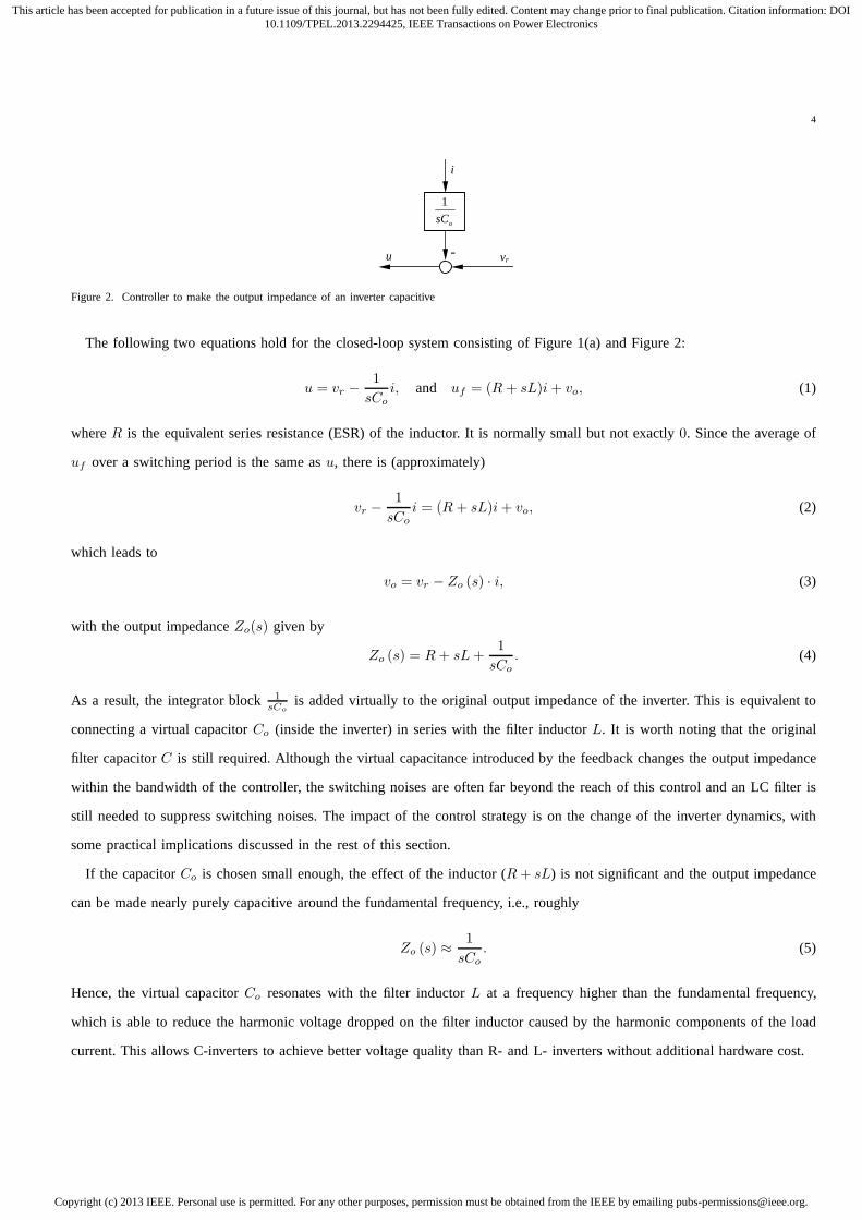
Here, the controller shown in Figure 2 is proposed to make theoutput impedance of an inverter capacitive.
Copyright (c) 2013 IEEE. Personal use is permitted. For any other purposes, permission must be obtained from the IEEE by emailing [email protected].
This article has been accepted for publication in a future issue of this journal, but has not been fully edited. Content may change prior to final publication. Citation information: DOI10.1109/TPEL.2013.2294425, IEEE Transactions on Power Electronics
4
osC
1
- u
i
vr
Figure 2. Controller to make the output impedance of an inverter capacitive
The following two equations hold for the closed-loop systemconsisting of Figure 1(a) and Figure 2:
u = vr −1
sCo
i, and uf = (R + sL)i+ vo, (1)
whereR is the equivalent series resistance (ESR) of the inductor. It is normally small but not exactly0. Since the average of
uf over a switching period is the same asu, there is (approximately)
vr −1
sCo
i = (R+ sL)i+ vo, (2)
which leads to
vo = vr − Zo (s) · i, (3)
with the output impedanceZo(s) given by
Zo (s) = R+ sL+1
sCo
. (4)
As a result, the integrator block1sCo
is added virtually to the original output impedance of the inverter. This is equivalent to
connecting a virtual capacitorCo (inside the inverter) in series with the filter inductorL. It is worth noting that the original
filter capacitorC is still required. Although the virtual capacitance introduced by the feedback changes the output impedance
within the bandwidth of the controller, the switching noises are often far beyond the reach of this control and an LC filteris
still needed to suppress switching noises. The impact of thecontrol strategy is on the change of the inverter dynamics, with
some practical implications discussed in the rest of this section.
If the capacitorCo is chosen small enough, the effect of the inductor (R+ sL) is not significant and the output impedance
can be made nearly purely capacitive around the fundamentalfrequency, i.e., roughly
Zo (s) ≈1
sCo
. (5)
Hence, the virtual capacitorCo resonates with the filter inductorL at a frequency higher than the fundamental frequency,
which is able to reduce the harmonic voltage dropped on the filter inductor caused by the harmonic components of the load
current. This allows C-inverters to achieve better voltagequality than R- and L- inverters without additional hardware cost.

Copyright (c) 2013 IEEE. Personal use is permitted. For any other purposes, permission must be obtained from the IEEE by emailing [email protected].
This article has been accepted for publication in a future issue of this journal, but has not been fully edited. Content may change prior to final publication. Citation information: DOI10.1109/TPEL.2013.2294425, IEEE Transactions on Power Electronics
5
B. Stability of the current loop
When the controller is implemented digitally, the effect ofcomputation and PWM conversion can be approximated by a
one-step delaye−sTs , whereTs is the sampling period. Hence, the approximate block diagram of the current loop can be
derived as shown in Figure 3(a). The corresponding open-loop transfer function is
L(s) =1
sCo
1
sL+Re−sTs , (6)
which has a pole ats = 0 but does not have any unstable poles in the right-half-planeof the s-domain. A typical Nyquist plot
of such systems is shown in Figure 3(b). In order to make sure that the system is stable, according to the well-known Nyquist
theorem, the plot should not encircle the critical point(−1, 0). Assume that the plot crosses the real axis for the first time at
the frequencyω0, thenω0 satisfies
−π
2− atan
ω0L
R− ω0Ts = −π. (7)
In other words,ω0 can be found as the first positive number from 0 that satisfies
R
ω0L= tan(ω0Ts). (8)
At this frequency, the loop gain 1
ω0Co
√ω2
0L2+R2
should be less than1. In other words, the loop is stable if
1
Co
< ω0
√
ω20L
2 +R2. (9)
It can be easily seen that
0 < ω0 <π
2Ts
. (10)
Hence, the current loop is stable if1
Co
<π
2Ts
√
(πL
2Ts
)2 +R2, (11)
of which the right-hand side is about( π2Ts
)2L for smallR ≈ 0. In other words, the loop is stable if the capacitanceCo or the
sampling frequencyfs = 1
Tsis chosen large enough so that the sampling frequencyfs is larger than four times the resonant
frequency 1
2π√LCo
with L, which can be easily met without any problem. Note thatR is not exactly zero in reality, which
helps maintain the stability of the loop.
C. DC offset in the system
Because of the presence of the integrator1
sCo, any DC offset in the currenti, e.g. that caused by the conversion process
or faults in the system etc., would lead to a DC offset in the output voltage. In order to avoid this problem, some simple
mechanisms can be adopted. For example, the integrator1
sCocan be reset when the inductor current passes zero if the offset
exceeds a given level. Alternatively, the integrator1sCo
can be slightly modified as 1
sCo+ǫwith a negligible positive number
ǫ ≈ 0. This is equivalent to putting a large resistor1
ǫin parallel withCo, which does not change the performance at non-DC

Copyright (c) 2013 IEEE. Personal use is permitted. For any other purposes, permission must be obtained from the IEEE by emailing [email protected].
This article has been accepted for publication in a future issue of this journal, but has not been fully edited. Content may change prior to final publication. Citation information: DOI10.1109/TPEL.2013.2294425, IEEE Transactions on Power Electronics
6
osC
1
- u
i
vr
RsL+1
sTse−
vo -
uf
0
0
Imag
inar
y A
xis
Real Axis
(a) Approximate block diagram (b) Typical Nyquist plot
Figure 3. The current loop
frequencies.
III. O PTIMISATION OF THE VOLTAGE QUALITY
Assume that the output current of the inverter is
i =√2Σ∞
h=1Ih sin(hωt+ φh), (12)
whereω is the system frequency. Then the amplitude of theh-th harmonic voltage dropped on the output impedance is√2Ih |Zo(jhω)|. Moreover, assume that the voltage referencevr is clean and sinusoidal and is described as
vr =√2E sin(ωt+ δ). (13)
Then the fundamental component of the output voltage is
v1 =√2E sin(ωt+ δ)−
√2I1 |Zo(jω)| sin(ωt+ φ1 + θ) (14)
=√2V1 sin(ωt+ β) (15)
with
V1=
√
E2 + I21 |Zo(jω)|2 − 2EI1 |Zo(jω)| cos(φ1 + θ − δ), (16)
β = arctan(ω |Zo(jω)| sin(φ1 + θ − δ)
I1 |Zo(jω)| cos(φ1 + θ − δ)− E). (17)
The sum of all harmonic components in the output voltage is
vH =√2Σ∞
h=2Ih |Zo(jhω)| sin(hωt+ φh + ∠Zo(jhω)). (18)
It is clear thatv1 and vH do not affect each other.v1 is determined by the clean reference voltage, the fundamental current
and the output impedance at the fundamental frequency.vH is determined by the harmonic current components and the output
impedance at the harmonic frequencies.

Copyright (c) 2013 IEEE. Personal use is permitted. For any other purposes, permission must be obtained from the IEEE by emailing [email protected].
This article has been accepted for publication in a future issue of this journal, but has not been fully edited. Content may change prior to final publication. Citation information: DOI10.1109/TPEL.2013.2294425, IEEE Transactions on Power Electronics
7
According to the definition of THD, the THD of the output voltage is
THD =
√
Σ∞h=2
I2h |Zo(jhω)|2
V1
× 100%. (19)
Hence, the THD is mainly affected by the output impedance at harmonic frequencies. As a result, it is feasible to optimise
the design of the output impedance at harmonic frequencies to minimise the THD of the output voltage.
For the C-inverter designed in the previous section, according to (4), there is
|Zo(jhω∗)|2 = R2 + (hω∗L− 1
hω∗Co
)2, (20)
whereω∗ is the rated angular system frequency. In order to minimise the THD of the output voltage, the virtual capacitorCo
should be chosen to minimise
Σ∞h=2I
2h |Zo(jhω
∗)|2 (21)
because the fundamental componentV1 can be assumed to be almost constant. This is equivalent to
minCo
Σ∞h=2i
21h(hω
∗L− 1
hω∗Co
)2, (22)
where i1h = IhI1
is the normalisedh-th harmonic currentIh with respect to the fundamental currentI1. Depending on the
distribution of the harmonic current components, different strategies can be obtained.
Assume that the harmonic current is negligible for the harmonics higher than theN -th order (with an odd numberN ). Then
Co can be found via solving (22). Define
f(Co) = ΣNh=2i
21h(hω
∗L− 1
hω∗Co
)2. (23)
ThenCo needs to satisfydf(Co)
dCo
= 2ΣNh=2i
21h(hω
∗L− 1
hω∗Co
)1
hω∗C2o
= 0, (24)
which is equivalent to
ΣNh=2i
21h(L− 1
(hω∗)2Co
) = 0. (25)
Hence,
ΣNh=2i
21hL =
1
(ω∗)2Co
ΣNh=2
i21hh2
, (26)
and the optimal capacitance can be solved as
Co =1
(ω∗)2L
ΣNh=2
i21h
h2
ΣNh=2
i21h
, (27)

Copyright (c) 2013 IEEE. Personal use is permitted. For any other purposes, permission must be obtained from the IEEE by emailing [email protected].
This article has been accepted for publication in a future issue of this journal, but has not been fully edited. Content may change prior to final publication. Citation information: DOI10.1109/TPEL.2013.2294425, IEEE Transactions on Power Electronics
8
which is applicable for any currenti with a known harmonic profile. The correspondingf(Co) is
fmin(Co) = ΣNh=2i
21h(hω
∗L− ω∗L
h
ΣNh=2i
21h
ΣNh=2
i21h
h2
)2
= (ω∗L)2ΣNh=2i
21h(h− 1
h
ΣNh=2i
21h
ΣNh=2
i21h
h2
)2. (28)
Hence, the THD ofvo is in proportion to the inductanceL of the inverter LC filter. A smallL does not only reduce the cost,
size, weight and volume of the inductor but also improves thevoltage quality. However, a smallL leads to a highdidt for the
switches and large current ripples. See the guidelines of selecting the components in the next section for details. Moreover,
since 1
Co∼ L, a smallL leads to a small gain for the integrator, which is good for thestability of the current loop.
If the distribution of the harmonic components is not known,then it can be assumed that the even harmonics are zero, which
is normally the case, and the odd harmonics are equally distributed. As a result, the optimalCo can be chosen, according to
(27), as
Co =1
(ω∗)2L
Σh=3, 5, 7, ...,N1
h2
ΣNh=3, 5, 7, ...,N1
(29)
=1
(ω∗)2L
Σh=3, 5, 7, ...,N1
h2
(N − 1)/2. (30)
This can be written as
Co =1
(ω∗)2L
1
(N − 1)/2(1
32+
1
52+ ...+
1
N2), (31)
where(N − 1)/2 is the number of terms in the summation. The correspondingf(Co) is
fmin(Co) = (ω∗L)2Σh=3, 5, 7, ...,N (h− 1
h
(N − 1)/2
Σh=3, 5, 7, ...,N1
h2
)2. (32)
If a singleh-th harmonic component is concerned, then the optimalCo is
Co =1
(hω∗)2L. (33)
This forces the impedance at theh-th harmonic frequency close to0 and hence no voltage at this frequency is caused,
assumingR = 0. According to the stability analysis carried out in the previous section, the current loop is stable in this case
if (hω∗)2L < ( π2Ts
)2L, or in other words iffs > 4hf∗, wheref∗ = ω∗
2πis the rated system frequency.
A. Special Case I: To minimise the 3rd and 5th harmonic components
In most cases, it is enough to consider the 3rd and 5th harmonics only. This gives the optimal capacitance
Co =17
225(ω∗)2L. (34)

Copyright (c) 2013 IEEE. Personal use is permitted. For any other purposes, permission must be obtained from the IEEE by emailing pubs−[email protected].
This article has been accepted for publication in a future issue of this journal, but has not been fully edited. Content may change prior to final publication. Citation information: DOI10.1109/TPEL.2013.2294425, IEEE Transactions on Power Electronics
9
As a result, the output impedance is
Zo(jω) = R + j(ωL− 1
ωCo
) (35)
= R + jω∗L(ω
ω∗− 225
17
ω∗
ω). (36)
The gain factorωω∗
− 225
17
ω∗
ωof the imaginary part with respect to the normalised frequency ω
ω∗is shown in Figure 4. It changes
from negative to positive at aroundωω∗
= 3.638. At the fundamental frequency, i.e., whenω = ω∗, the output impedance is
Zo = R− j208
17ω∗L ≈ −j12.23ω∗L. (37)
It is capacitive as expected becauseR is normally smaller thanω∗L.
B. Special Case II: To minimise the 3rd harmonic component
In this case, the optimalCo is
Co =1
(3ω∗)2L(38)
and the corresponding impedance is
Zo(jω) = R+ j(ωL− 1
ωCo
) (39)
= R+ jω∗L(ω
ω∗− 9ω∗
ω). (40)
The gain factor ωω∗
− 9ω∗
ωof the imaginary part with respect to the normalised frequency ω
ω∗is also shown in Figure 4. It
changes from negative to positive atω = 3ω∗. At the fundamental frequency, i.e., whenω = ω∗, the output impedance is
Zo = R− j8ω∗L ≈ −j8ω∗L, (41)
which is capacitive as well.
1 1.5 2 2.5 3 3.5 4 4.5 5 5.5 6 6.5 7−14−12−10−8−6−4−2
0246
ω/ω*
The
gai
n fa
ctor
Original inductor
3rd and 5th
3rd only
5th only
Figure 4. The gain factors to meet different criteria

Copyright (c) 2013 IEEE. Personal use is permitted. For any other purposes, permission must be obtained from the IEEE by emailing [email protected].
This article has been accepted for publication in a future issue of this journal, but has not been fully edited. Content may change prior to final publication. Citation information: DOI10.1109/TPEL.2013.2294425, IEEE Transactions on Power Electronics
10
C. Special Case III: To minimise the 5th harmonic component
In this case, the optimalCo is
Co =1
(5ω∗)2L(42)
and the corresponding impedance is
Zo(jω) = R+ j(ωL− 1
ωCo
) (43)
= R+ jω∗L(ω
ω∗− 25ω∗
ω). (44)
The gain factor ωω∗
− 25ω∗
ωof the imaginary part with respect to the normalised frequency ω
ω∗is also shown in Figure 4. It
changes from negative to positive atω = 5ω∗. At the fundamental frequency, i.e., whenω = ω∗, the output impedance is
Zo = R− j24ω∗L ≈ −j24ω∗L. (45)
This is capacitive as well.
IV. COMPONENT SELECTION
A. Selection of the filter inductorL
As discovered in the previous section, the smaller the filterinductor, the smaller the output impedance and the better the
voltage quality. Thus, it is better to have a small output inductor than a big one. This leaves the selection of the filter inductor
to meet the requirement on the allowed current ripples only.According to [23], it is recommended that the current ripples
should satisfy
0.15 6∆I
Iref6 0.4, (46)
with
∆I =Udc
4Lfs, (47)
where∆I is the inductor current ripple andIref is the rated peak current at the fundamental frequency. Thus, the inductor
should be chosen to satisfy5Udc
8fsIref6 L 6
5Udc
3fsIref. (48)
This could be applied to analyse the impact on the DC-bus voltage. For example, assume thatL is selected to achieve the
maximum current ripple of0.4Iref . Moreover, . assume that the peak of theh-th harmonic current reaches50% of Iref .. Then
the voltage drop of theh-th harmonic current on the inductor ishω∗ 5Udc
8fsIref× Iref
2= 5hω∗
16fsUdc. In other words, the maximum
increase of the required DC bus voltage is5hω∗
16fs× 100%. For h = 5, fs = 10kHz andω∗ = 100πrad/sec, this is4.9% so it is
not demanding at all and there is no need to take any special action when determining the DC bus voltage.

Copyright (c) 2013 IEEE. Personal use is permitted. For any other purposes, permission must be obtained from the IEEE by emailing [email protected].
This article has been accepted for publication in a future issue of this journal, but has not been fully edited. Content may change prior to final publication. Citation information: DOI10.1109/TPEL.2013.2294425, IEEE Transactions on Power Electronics
11
B. Selection of the filter capacitorC
The main function of the LC filter is to attenuate the harmonics generated by the PWM conversion and the H-bridge via
re-producing the control signalu, especially the harmonics around the switching frequencyfs. When there is no load, the
transfer function betweenuf andvo is
H(s) =1
s2LC + 1. (49)
Indeed, the virtual capacitorCo does not change the role of the LC filter in suppressing the switching noises because the actual
output voltageuf generated by the inverter is still passed through the LC filter. The cut-off frequencyfc can be found from
|H(j2πfc)| =1
|1− (2πfc)2LC| =1√2
(50)
as
fc =1
2π√LC
√√2 + 1, (51)
which is about1.5 times of the resonant frequency 1
2π√LC
. Since it is very close to the resonant frequency, it is reasonable
to use the resonant frequency when selecting the components.
The overall output impedanceZ(s) after taking into account the filter capacitorC is
Z(s) =Zo(s)
1
sC
Zo(s) +1
sC
=Zo(s)
sCZo(s) + 1. (52)
At low frequencies, there is
Z(s) ≈ Zo(s) = R+ sL+1
sCo
(53)
and at high frequencies, there is
Z(s) ≈ 1
sC. (54)
This actually verifies that the definition of the output impedanceZo without considering the filter capacitorC does not materially
affect the analysis at low frequencies. Defining the output impedance at the terminal with the output voltage and the filter
inductor current is simply to facilitate the presentation.
For conventional inverters, which are mainly L-inverters,Z(s) is inductive at low frequencies. Hence, the overall output
impedanceZ(s) changes its type from inductive to capacitive at the resonant frequency. However, according to (52), the overall
output impedanceZ(s) for the C-inverters designed above is
Z(s) =sL+R+ 1
sCo
s2LC + sCR+ CCo
+ 1. (55)
It is capacitive at both low frequencies (1sCo
) and high frequencies (1sC
). In order to better demonstrate this, the Bode plots of
the overall output impedances of typical L- and C-invertersare shown in Figure 5. The output impedance of the C-inverteris
capacitive over a wide range of both low and high frequenciesand is inductive only over a small range of mid-frequencies.
There is a series resonance betweenL andCo, in addition to the parallel resonance betweenL andC, which is slightly changed

Copyright (c) 2013 IEEE. Personal use is permitted. For any other purposes, permission must be obtained from the IEEE by emailing pubs−[email protected].
This article has been accepted for publication in a future issue of this journal, but has not been fully edited. Content may change prior to final publication. Citation information: DOI10.1109/TPEL.2013.2294425, IEEE Transactions on Power Electronics
12
because ofCo. The output impedance of the L-inverter is inductive for lowfrequencies up to the resonant frequency of the
filter and capacitive for the frequencies above.
−40
−20
0
20
40
60
Mag
nitu
de (
dB)
101
102
103
104
105
106
−90
−45
0
45
90
Pha
se (
deg)
Bode Diagram
Frequency (rad/sec)
C−inverter
L−inverter
Figure 5. Overall output impedance of an L-inverter and a C-inverter after taking into account the filter capacitorC
The optimisation of the voltage quality discussed in the previous subsection is achieved via tuning the series resonance
betweenL andCo. Since the load currentio may include a large amount of harmonic components, especially when the load
is nonlinear, the parallel resonance betweenL, C andCo should be considered when designing the filter. According to(55),
the parallel resonant frequencyfr can be obtained as
fr =1
2π
√
C + Co
LCCo
=1
2π√LC
√
C
Co
+ 1. (56)
With the sameL andC, the resonance frequencyfr of C-inverters is higher than, but very close to, that of the corresponding
L-inverter or R-inverters, which is 1
2π√LC
, becauseCo is often much larger thanC. In order to avoid amplifying some harmonic
current components, the resonance frequencyfr is recommended to be chosen between 10 times the line frequency ω∗ and
half of the switching frequencyfs [23]. Hence,fr is often far away from the harmonics to be eliminated by designing Co.
Indeed, ifCo is designed to eliminate theh-th harmonic, then according to (56), there is
fr =1
2π√LCo
√
Co
C+ 1 =
hω∗
2π
√
Co
C+ 1. (57)
That is, the resonant frequency is√
Co
C+ 1 times the harmonic frequencyhω∗ under control. If
√
Co
C+ 1 > 3, thenfr > 3hω∗
2π
and it is over 9 times the system frequencyω∗ even forh = 3. Hence, it is recommended to selectfr to satisfy
3hω∗
2π6 fr 6
1
2fs, (58)
that is to select the parallel resonant frequency between three times of the harmonic frequency under control and half ofthe

Copyright (c) 2013 IEEE. Personal use is permitted. For any other purposes, permission must be obtained from the IEEE by emailing [email protected].
This article has been accepted for publication in a future issue of this journal, but has not been fully edited. Content may change prior to final publication. Citation information: DOI10.1109/TPEL.2013.2294425, IEEE Transactions on Power Electronics
13
switching frequency. Accordingly, it is recommended to select the filter capacitorC to satisfy
3hω∗
2π6
hω∗
2π
√
Co
C+ 1 6
1
2fs
or, equivalently,Co
( πfshω∗
)2 − 16 C 6
1
8Co. (59)
+
vri
s
1
ω
*
vo
i
Ei
ω it+δ i
Pi ni
mi
eK -
E*
RMS
s
1
+
Qi
Pow
erC
alcu
latio
n
Figure 6. The robust droop controller for C-inverters [31] to generate the voltage referencevr
V. SIMULATION RESULTS
Simulations were carried out with a single-phase inverter powered by a 350V DC voltage supply. The switching frequency
is 10kHz and the system frequency is50Hz. The rated output voltage is230V and the rated peak current is chosen as 40A.
Thus the rated apparent power of the inverter is 6.5 kVA. The load is a full-bridge rectifier loaded with an LC filter (2.2mH ,
150µF ) and a resistorRL = 30Ω. An extra load consisting of a200Ω resistor and a22mH inductor in series is connected
at t = 2s, and disconnected att = 9s to test the transient response of C-inverters, R-invertersand L-inverters. The inverter
reference voltage was generated by the robust droop controller proposed in [31], which is shown in Figure 6 for convenience.
As can be seen from Figure 6, at the steady state, there is
Ke(E∗ − Vo) = niPi,
whereVo is the RMS value of the output voltage. As a result, the RMS output voltage is
Vo = E∗ − ni
Ke
Pi,
which shows that the output voltage is regulated and the voltage error could be maintained small via choosing a largeKe.
Hence, there is no need to have an extra voltage loop to regulate the instantaneous output voltage. The parameters of the robust
droop controller were chosen asni = 6.3× 10⁻⁴, mi = 3.4× 10⁻⁵ andKe = 10, according to [31].
According to (48), the filter inductor should be chosen between 0.55mH and1.46mH. To make the output voltage THD
small, the inductor is chosen as0.55mH. The virtual capacitorCo is chosen to be1400µF to reduce the 3rd and 5th harmonics.

Copyright (c) 2013 IEEE. Personal use is permitted. For any other purposes, permission must be obtained from the IEEE by emailing pubs−[email protected].
This article has been accepted for publication in a future issue of this journal, but has not been fully edited. Content may change prior to final publication. Citation information: DOI10.1109/TPEL.2013.2294425, IEEE Transactions on Power Electronics
14
0 1 2 3 4 5 6 7 8 9 100
5001000150020002500
P [W
]
Time [s]
1.9 2 2.1 2.2170019502200
0 1 2 3 4 5 6 7 8 9 100
5001000150020002500
P [W
]
Time [s]
1.9 2 2.1 2.2170019502200
0 1 2 3 4 5 6 7 8 9 100
5001000150020002500
P [W
]
Time [s]
1.9 2 2.1 2.2170019502200
(a) Active power
0 1 2 3 4 5 6 7 8 9 10−1500−1200−900−600−300
0
Q [V
ar]
Time [s]0 1 2 3 4 5 6 7 8 9 10
−1500−1200−900−600−300
0
Q [V
ar]
Time [s]0 1 2 3 4 5 6 7 8 9 10
−1500−1200−900−600−300
0
Q [V
ar]
Time [s]
(b) Reactive power
0 1 2 3 4 5 6 7 8 9 1049.9849.99
5050.0150.02
Fre
quen
cy [H
z]
Time [s]0 1 2 3 4 5 6 7 8 9 10
49.9849.99
5050.0150.02
Fre
quen
cy [H
z]
Time [s]0 1 2 3 4 5 6 7 8 9 10
49.9849.99
5050.0150.02
Fre
quen
cy [H
z]
Time [s]
(c) Frequency
0 1 2 3 4 5 6 7 8 9 100
50100150200250
Vo [V
]
Time [s]0 1 2 3 4 5 6 7 8 9 10
050
100150200250
Vo [V
]
Time [s]0 1 2 3 4 5 6 7 8 9 10
050
100150200250
Vo [V
]
Time [s]
(d) Output Voltage RMSVo
1.98 2 2.02 2.04 2.06 2.08 2.1−400−200
0200400
v o [V]
Time [s]1.98 2 2.02 2.04 2.06 2.08 2.1
−400−200
0200400
v o [V]
Time [s]1.98 2 2.02 2.04 2.06 2.08 2.1
−400−200
0200400
v o [V]
Time [s]
(e) Output Voltagevo
0 1 2 3 4 5 6 7 8 9 1002468
10
TH
D o
f vo (
%)
Time [s]0 1 2 3 4 5 6 7 8 9 10
02468
10
TH
D o
f vo (
%)
Time [s]0 1 2 3 4 5 6 7 8 9 10
02468
10
TH
D o
f vo (
%)
Time [s]
(f) THD of output Voltagevo
1.98 2 2.02 2.04 2.06 2.08 2.1−40−20
02040
Cur
rent
[A]
Time [s]1.98 2 2.02 2.04 2.06 2.08 2.1
−40−20
02040
Cur
rent
[A]
Time [s]1.98 2 2.02 2.04 2.06 2.08 2.1
−40−20
02040
Cur
rent
[A]
Time [s]
(g) Inductor currenti
Figure 7. Simulation results with the extra load consistingof a 200Ω resistor and a22mH inductor in series connected att = 2s and disconnected att = 9s:C-inverter withCo = 1400µF to reduce the 3rd and the 5th harmonics (left column),R-inverter withKi = 4 (middle column) andL-inverter (rightcolumn)
According to (59), the filter capacitorC should satisfy
1.84µF 6 C 6 174µF, (60)
from which the filter capacitor was selected asC = 20µF .
The simulation results of the C-inverter, together with those of an L-inverter and a R-inverter withKi = 4, are shown in
Figure 7. The C-inverter achieves lowest output voltage THDamong the three types of inverters. When the extra load of a
200Ω resistor and a22mH inductor in series is connected or disconnected, all the three type of inverter are able to respond
fast and reach the steady state quickly and smoothly. It can be seen that the transient response of the C-inverter is better than

Copyright (c) 2013 IEEE. Personal use is permitted. For any other purposes, permission must be obtained from the IEEE by emailing [email protected].
This article has been accepted for publication in a future issue of this journal, but has not been fully edited. Content may change prior to final publication. Citation information: DOI10.1109/TPEL.2013.2294425, IEEE Transactions on Power Electronics
15
the other two.
VI. EXPERIMENTAL VALIDATION
Experiments were carried out with a single-phase inverter powered by a 180V DC voltage supply, which was obtained from
a non-regulated diode rectifier. The switching frequency and the system frequency are the same with the ones used in the
simulation, respectively. The rated output voltage is110V and the rated peak current is 8A. The load is a full-bridge rectifier
loaded with an LC filter (2.2mH , 150µF ) and a resistorRL = 200Ω. The inverter reference voltage was also generated
by the robust droop controller [31] shown in Figure 6 , and theparameters of the robust droop controller were chosen as
ni = 3.4× 10⁻³, mi = 3.9× 10⁻⁴ andKe = 10.
According to (48), the filter inductor should be chosen between1.41mH and3.75mH. The inductor2.2mH on board on-board
the inverter falls into this range. Three different cases with the virtual capacitorCo chosen to reduce the 3rd harmonic, the
5th harmonic, and both the 3rd and the 5th harmonics, respectively, were tested. The corresponding virtual capacitanceCo is
512µF, 184µF and348µF, respectively. According to (59), the filter capacitorC should satisfy
0.46µF 6 C 6 23µF. (61)
The filter capacitorC = 10µF on-board the inverter falls into this range. The corresponding resonant frequency is1131Hz
for the case withh = 5 and1083Hz for the case withh = 3, which leaves enough room for a normal switching frequency,
e.g. 5kHz.
The experimental results are shown in Figure 8, together with those from an R-inverter withZo = 4Ω and an L-inverter
designed according to the current feedback controller proposed in [37] withKi = 4 andKi = 0, respectively, for comparison.
When the inverter was designed to have capacitive output impedance to reduce the effect of the 3rd and the 5th harmonics, the
3rd harmonic was reduced by about50% from the case of the L-inverter and by about65% from the case of the R-inverter,
and the 5th harmonic was reduced by about30% and 18%, respectively. The THD was reduced by about40% and 50%,
respectively. When the inverter was designed to have capacitive output impedance to minimise the effect of the 3rd harmonic,
the 3rd harmonic was reduced by63% from the case of the L-inverter and by74% from the case of the R-inverter, respectively.
The THD was reduced by about36% and by47%, respectively .When the inverter was designed to have capacitive output
impedance to minimise the effect of the 5th harmonic, the 5thharmonic was reduced by41% from the case of the L-inverter and
by 31% from the case of the R-inverter, respectively. The THD was reduced by about37% and48%, respectively. Apparently,
C-inverters performed much better than the R- and L-inverters. Moreover, the THD is the lowest whenCo is designed to
optimise the 3rd and 5th harmonics than to optimise these twoseparately. This is because the major harmonic components of
the load current are the 3rd and the 5th harmonics, as can be seen from Figure 8(e).
The recorded average RMS values of the output voltage are 109.7V for the R-inverter, 110.2V for the L-inverter and 109.8V
for the C-inverters, which shows the excellent voltage regulation capability of the robust droop control strategy. This is true
regardless of the virtual capacitance concept.

Copyright (c) 2013 IEEE. Personal use is permitted. For any other purposes, permission must be obtained from the IEEE by emailing [email protected].
This article has been accepted for publication in a future issue of this journal, but has not been fully edited. Content may change prior to final publication. Citation information: DOI10.1109/TPEL.2013.2294425, IEEE Transactions on Power Electronics
16
VII. C ONCLUSIONS ANDDISCUSSIONS
It has been shown that it is feasible to force the output impedance of an inverter to be capacitive over a wide range of
both low and high frequencies although it normally has an inductor connected to the inverter bridge. Such inverters are called
C-inverters. One simple but effective approach is to form aninductor current feedback through an integrator, of which the
time constant is the desired output capacitance. This is a virtual capacitor so there is no limit on the current rating andcan
be applied to any power level. The capacitance can be selected to guarantee the stability of the current loop and an algorithm
is proposed to optimise the value of the output capacitance so that the THD of the output voltage is minimised. Detailed
guidelines have been provided to place the relevant frequencies properly so that the filter components can be determined.
Extensive experimental results have shown that the THD of aninverter can be reduced when it is designed to have capacitive
output impedance, with comparison to an inverter having resistive or inductive output impedance. Moreover, no visibleDC
offsets are seen from the experimental results. One by-product of this study is that the filter inductor should be chosen small
in order to reduce voltage harmonics and the criterion is reduced to meet the current ripples allowed on the inductor. A small
inductor helps reduce the size, weight and volume of the passive components needed.
Since the C-inverter concept is completely new, some issuesshould be further investigated, in particular, for grid-connected
applications. For example, because of the introduction of acapacitor into the output impedance, a natural question is whether
this would lead to possible resonance with the rest of the system (such as the line, loads, etc.). This may not be an issue because
in flexible AC transmission systems (FACTS), capacitors have been physically connected in series with transmission lines to
improve the line capacity. Another question is whether thiswill affect the current quality for grid-connected applications. It
has been found that C-inverters offer the lowest output voltage THD among R-, L- and C-inverters with the same hardware.
Further investigations should be carried out to explore other advantages and applications of C-inverters.
ACKNOWLEDGEMENTS
The authors are grateful to the Reviewers and Editors for their detailed comments, which have considerably improved the
quality of the paper. Yokogawa Measurement Technologies Ltd is greatly appreciated for the donation of a high-precision
wide-bandwidth power meter WT1600 and a digital 8-channel oscilloscope DL7480.
REFERENCES
[1] Q.-C. Zhong and T. Hornik,Control of Power Inverters in Renewable Energy and Smart Grid Integration. Wiley-IEEE Press, 2013.
[2] DOE, “The smart grid: An introduction,” The U.S. Department of Energy, Tech. Rep., http://energy.gov/sites/prod/files/oeprod/DocumentsandMedia/D
OE_SG_Book_Single_Pages.pdf.
[3] Z. Liu, J. Liu, and Y. Zhao, “A unified control strategy forthree-phase inverter in distributed generation,”IEEE Trans. Power Electron., vol. 29, no. 3,
pp. 1176–1191, 2014.
[4] J. Kwon, S. Yoon, and S. Choi, “Indirect current control for seamless transfer of three-phase utility interactive inverters,” IEEE Trans. Power Electron.,
vol. 27, no. 2, pp. 773–781, 2012.
[5] C. Bao, X. Ruan, X. Wang, W. Li, D. Pan, and K. Weng, “Step-by-step controller design for LCL-type grid-connected inverter with capacitor current-
feedback active-damping,”IEEE Trans. Power Electron., vol. 29, no. 3, pp. 1239–1253, 2014.
[6] I. Nutkani, P. C. Loh, and F. Blaabjerg, “Droop scheme with consideration of operating costs,”IEEE Trans. Power Electron., vol. 29, no. 3, pp. 1047–1052,
2014.

Copyright (c) 2013 IEEE. Personal use is permitted. For any other purposes, permission must be obtained from the IEEE by emailing [email protected].
This article has been accepted for publication in a future issue of this journal, but has not been fully edited. Content may change prior to final publication. Citation information: DOI10.1109/TPEL.2013.2294425, IEEE Transactions on Power Electronics
17
[7] F. Blaabjerg, R. Teodorescu, M. Liserre, and A. Timbus, “Overview of control and grid synchronization for distributed power generation systems,”IEEE
Trans. Ind. Electron., vol. 53, no. 5, pp. 1398–1409, Oct. 2006.
[8] A. V. Timbus, R. Teodorescu, F. Blaabjerg, M. Liserre, and P. Rodriguez, “Linear and nonlinear control of distributed power generation systems,” in
Proc. of IEEE Industry Applications Conference, 2006, pp. 1015–1023.
[9] A. Kavousi, B. Vahidi, R. Salehi, M. Bakhshizadeh, N. Farokhnia, and S. Fathi, “Application of the bee algorithm for selective harmonic elimination
strategy in multilevel inverters,”IEEE Trans. Power Electron., vol. 27, no. 4, pp. 1689–1696, 2012.
[10] Y. Ye, B. Zhang, K. Zhou, D. Wang, and Y. Wang, “High-performance cascade-type repetitive controller for CVCF PWM inverter: Analysis and design,”
IET Proc. Electric Power Appli., vol. 1, no. 1, pp. 112–118, Jan. 2007.
[11] ——, “High-performance repetitive control of PWM DC-ACconverters with real-time phase lead FIR filter,”IEEE Trans. Circuits Syst., vol. 53, no. 8,
pp. 768–772, Aug. 2006.
[12] Y. Wang, D. Wang, B. Zhang, and K. Zhou, “Fractional delay based repetitive control with application to PWM DC/AC converters,” inProc. of IEEE
International Conference on Control Applications, 2007.
[13] B. Zhang, D. Wang, K. Zhou, and Y. Wang, “Linear phase lead compensation repetitive control of a CVCF PWM inverter,”IEEE Trans. Ind. Electron.,
vol. 55, no. 4, pp. 1595–1602, Apr. 2008.
[14] S. Chen, Y. Lai, S.-C. Tan, and C. Tse, “Analysis and design of repetitive controller for harmonic elimination in PWMvoltage source inverter systems,”
IET Proc. Power Electron., vol. 1, no. 4, pp. 497–506, Dec. 2008.
[15] Y.-Y. Tzou, S.-L. Jung, and H.-C. Yeh, “Adaptive repetitive control of PWM inverters for very low THD AC-voltage regulation with unknown loads,”
IEEE Trans. Power Electron., vol. 14, no. 5, pp. 973–981, Sept. 1999.
[16] S. Jiang, D. Cao, Y. Li, J. Liu, and F.-Z. Peng, “Low-THD,fast-transient, and cost-effective synchronous-frame repetitive controller for three-phase UPS
inverters,” IEEE Trans. Power Electron., vol. 27, no. 6, pp. 2994–3005, 2012.
[17] T. Hornik and Q.-C. Zhong, “H∞ repetitive voltage control of grid-connected inverters with frequency adaptive mechanism,”IET Proc. Power Electron.,
vol. 3, no. 6, pp. 925–935, Nov. 2010.
[18] G. Weiss, Q.-C. Zhong, T. Green, and J. Liang, “H∞ repetitive control of DC-AC converters in micro-grids,”IEEE Trans. Power Electron., vol. 19,
no. 1, pp. 219–230, Jan. 2004.
[19] Q.-C. Zhong, “Harmonic droop controller to reduce the voltage harmonics of inverters,”IEEE Trans. Ind. Electron., vol. 60, no. 3, pp. 936–945, Mar.
2013.
[20] U. Borup, F. Blaabjerg, and P. Enjeti, “Sharing of nonlinear load in parallel-connected three-phase converters,”IEEE Trans. Ind. Appl., vol. 37, no. 6,
pp. 1817–1823, Nov./Dec. 2001.
[21] Q.-C. Zhong, F. Blaabjerg, J. Guerrero, and T. Hornik, “Reduction of voltage harmonics for parallel-operated inverters,” in Proc. of IEEE Energy
Conversion Congress and Exposition (ECCE), 2011, pp. 473–478.
[22] S. Dewan, “Optimum input and output filters for a single-phase rectifier power supply,”IEEE Trans. Ind. Appl., vol. 17, no. 3, pp. 282–288, 1981.
[23] W. Wu, Y. He, and F. Blaabjerg, “An LLCL power filter for single-phase grid-tied inverter,”IEEE Trans. Power Electron., vol. 27, no. 2, pp. 782–789,
2012.
[24] W. Wu, Y. He, T. Tang, and F. Blaabjerg, “A new design method for the passive damped LCL and LLCL filter-based single-phase grid-tied inverter,”
IEEE Trans. Ind. Electron., vol. 60, no. 10, pp. 4339–4350, 2013.
[25] S. Gomez Jorge, C. Busada, and J. Solsona, “Frequency adaptive discrete filter for grid synchronization under distorted voltages,”IEEE Trans. Power
Electron., vol. 27, no. 8, pp. 3584–3594, 2012.
[26] J. M. Guerrero, L. G. de Vicuna, J. Matas, M. Castilla, and J. Miret, “Output impedance design of parallel-connectedUPS inverters with wireless
load-sharing control,”IEEE Trans. Ind. Electron., vol. 52, no. 4, pp. 1126–1135, May. 2005.
[27] J. M. Guerrero, J. Matas, L. G. de Vicuna, M. Castilla, and J. Miret, “Decentralized control for parallel operation of distributed generation inverters
using resistive output impedance,”IEEE Trans. Ind. Electron., vol. 54, no. 2, pp. 994–1004, Nov. 2007.
[28] J. Guerrero, L. de Vicuna, J. Miret, J. Matas, and J. Cruz, “Output impedance performance for parallel operation of UPS inverters using wireless and
average current-sharing controllers,” inProc. of the 35th IEEE Power Electronics Specialists Conference, 2004, pp. 2482–2488.
[29] J. He and Y. W. Li, “Generalized closed-loop control schemes with embedded virtual impedances for voltage source converters with lc or lcl filters,”
IEEE Trans. Power Electron., vol. 27, no. 4, pp. 1850–1861, 2012.
Copyright (c) 2013 IEEE. Personal use is permitted. For any other purposes, permission must be obtained from the IEEE by emailing [email protected].
This article has been accepted for publication in a future issue of this journal, but has not been fully edited. Content may change prior to final publication. Citation information: DOI10.1109/TPEL.2013.2294425, IEEE Transactions on Power Electronics
18
[30] Y. Zhang, M. Yu, F. Liu, and Y. Kang, “Instantaneous current-sharing control strategy for parallel operation of upsmodules using virtual impedance,”
IEEE Trans. Power Electron., vol. 28, no. 1, pp. 432–440, 2013.
[31] Q.-C. Zhong and Y. Zeng, “Can the output impedance of an inverter be designed capacitive?” inProc. of the 37th Annual IEEE Conference of Industrial
Electronics (IECON), 2011.
[32] Q.-C. Zhong, “Active capacitors: Concept and implementation,” in Proc. of IEEE International Symposium on Industrial Electronics (ISIE), Hangzhou,
China, May 2012.
[33] M. J. Ryan, W. E. Brumsickle, and R. D. Lorenz, “Control topology options for single-phase UPS inverters,”IEEE Trans. Ind. Appl., vol. 33, no. 2, pp.
493–501, 1997.
[34] D. Neacsu, “Line voltage compensation for ac output converters,” in 34th Annual Conference of IEEE on Industrial Electronics (IECON), 2008, pp.
3149–3154.
[35] S. Manias, E. P. Wiechmann, and P. Ziogas, “Effects of switching angle phase shift on pwm techniques,”IEEE Trans. Ind. Electron., vol. 34, no. 4, pp.
463–470, 1987.
[36] Y. Wu, M. Shafi, A. Knight, and R. McMAHON, “Comparison ofthe effects of continuous and discontinuous pwm schemes on power losses of
voltage-sourced inverters for induction motor drives,”IEEE Trans. Power Electron., vol. 26, no. 1, pp. 182–191, 2011.
[37] Q.-C. Zhong, “Robust droop controller for accurate proportional load sharing among inverters operated in parallel,” IEEE Trans. Ind. Electron., vol. 60,
no. 4, pp. 1281–1290, Apr. 2013.
[38] H. Patel and V. Agarwal, “Control of a stand-alone inverter-based distributed generation source for voltage regulation and harmonic compensation,”
IEEE Trans. Power Del., vol. 23, no. 2, pp. 1113–1120, 2008.
[39] J. Sun, “Impedance-based stability criterion for grid-connected inverters,”IEEE Trans. Power Electron., vol. 26, no. 11, pp. 3075–3078, 2011.
[40] J. Matas, M. Castilla, L. de Vicuna, J. Miret, and J. Vasquez, “Virtual impedance loop for droop-controlled single-phase parallel inverters using a
second-order general-integrator scheme,”IEEE Trans. Power Electron., vol. 25, no. 12, pp. 2993–3002, 2010.
Qing-Chang Zhong is the Chair Professor in Control and Systems Engineering atthe Department of
Automatic Control and Systems Engineering, The Universityof Sheffield, UK. He is a Distinguished
Lecturer of IEEE Power Electronics Society and is invited torepresent the UK at the European Control
Association. In 2012-2013, he spent a six-month sabbaticalat the Cymer Center for Control Systems
and Dynamics (CCSD), University of California, San Diego, USA and an eight-month sabbatical at the
Center for Power Electronics Systems (CPES), Virginia Tech, Blacksburg, USA. He received his PhD
degree in control and power engineering (awarded the Best Doctoral Thesis Prize) from Imperial College
London, London, UK, in 2004, and a PhD degree in control theory and engineering from Shanghai
Jiao Tong University in 2000. He (co-)authored three research monographs: Control of Power Inverters
in Renewable Energy and Smart Grid Integration (Wiley-IEEEPress, 2013), Robust Control of Time-
Delay Systems (Springer-Verlag, 2006), Control of Integral Processes with Dead Time (Springer-Verlag,
2010). His fourth research monograph entitled Completely Autonomous Power Systems (CAPS): Next Generation Smart Grids
is scheduled to appear in 2015. He, jointly with G. Weiss, invented the synchronverter technology to operate inverters to mimic
synchronous generators, which was awarded Highly Commended at the 2009 IET Innovation Awards. He is the architect of
the next-generation smart grid and a Specialist recognisedby the State Grid Corporation of China (SGCC), a Fellow of the
Institution of Engineering and Technology (IET), a Senior Member of IEEE, the Vice-Chair of IFAC TC 6.3 (Power and Energy
Systems) and was a Senior Research Fellow of the Royal Academy of Engineering/Leverhulme Trust, UK (2009–2010). He
serves as an Associate Editor for IEEE Transactions on PowerElectronics, IEEE Access and the Conference Editorial Board
of the IEEE Control Systems Society. His research focuses onadvanced control theory and its applications in various sectors,

Copyright (c) 2013 IEEE. Personal use is permitted. For any other purposes, permission must be obtained from the IEEE by emailing [email protected].
This article has been accepted for publication in a future issue of this journal, but has not been fully edited. Content may change prior to final publication. Citation information: DOI10.1109/TPEL.2013.2294425, IEEE Transactions on Power Electronics
19
including power electronics, renewable energy and smart grid integration, electric drives and electric vehicles, robust and
H-infinity control, time-delay systems, process control, mechatronics.
Yu Zeng received the B.Eng. degree in automation from Central SouthUniversity, Changsha, China,
in 2009. She is currently working toward the Ph.D. degree from the Department of Automatic Control
and Systems Engineering, the University of Sheffield, Sheffield, UK. Her research interests include
control of power electronic systems, microgrids and distributed generation, in particular, the parallel
operation of inverters.

Copyright (c) 2013 IEEE. Personal use is permitted. For any other purposes, permission must be obtained from the IEEE by emailing pubs−[email protected].
This article has been accepted for publication in a future issue of this journal, but has not been fully edited. Content may change prior to final publication. Citation information: DOI10.1109/TPEL.2013.2294425, IEEE Transactions on Power Electronics
20
i: [2A/div]
vo: [60V/div]
t: [8ms/div]
3 5 7 9 11131517192123252729310
1%
2%
3%
4%
5% THD 3.47%
TH
D o
f vo (
%)
Harmonic order
(a) C-inverter withCo = 348µF to reduce the 3rd and the 5th harmonics
i: [2A/div]
vo: [60V/div]
t: [8ms/div]
3 5 7 9 11131517192123252729310
1%
2%
3%
4%
5% THD 3.72%
TH
D o
f vo (
%)
Harmonic order
(b) C-inverter withCo = 512µF to reduce the 3rd harmonic
i: [2A/div]
vo: [60V/div]
t: [8ms/div]
3 5 7 9 11131517192123252729310
1%
2%
3%
4%
5% THD 3.63%
TH
D o
f vo (
%)
Harmonic order
(c) C-inverter withCo = 184µF to reduce the 5th harmonic
i: [2A/div]
vo: [60V/div]
t: [8ms/div]
3 5 7 9 11131517192123252729310
1%
2%
3%
4%
5% THD 7.03%
TH
D o
f vo (
%)
Harmonic order
(d) R-inverter withKi = 4
i: [2A/div]
vo: [60V/div]
t: [8ms/div]
3 5 7 9 11131517192123252729310
1%
2%
3%
4%
5% THD 5.8%
TH
D o
f vo (
%)
Harmonic order
(e) L-inverter
Figure 8. Experimental results: output voltagevo and inductor currenti (left column), harmonic distribution ofvo (right column)