tpa6111a2 150-mw stereo audio power amplifier · mw of continuous rms power per channel into 16-Ω...
TRANSCRIPT

AudioInput
BiasControl
8
1
7
4
VO1
VO2
VDD
5
2
3
6
IN1−
BYPASS
SHUTDOWN
VDD/2
CI
RI
RF
C(BYP)
C(S)
AudioInput
CI
RI IN2−
RF
VDD
From ShutdownControl Circuit
−+
−+
C(C)
C(C)
Product
Folder
Sample &Buy
Technical
Documents
Tools &
Software
Support &Community
An IMPORTANT NOTICE at the end of this data sheet addresses availability, warranty, changes, use in safety-critical applications,intellectual property matters and other important disclaimers. PRODUCTION DATA.
TPA6111A2SLOS313C –DECEMBER 2000–REVISED MARCH 2016
TPA6111A2 150-mW Stereo Audio Power Amplifier
1
1 Features1• 150-mW Stereo Output• PC Power Supply Compatible
– Fully Specified for 3.3-V and5-V Operation
– Operation to 2.5 V• Pop Reduction Circuitry• Internal Midrail Generation• Thermal and Short-Circuit Protection• Surface-Mount Packaging
– PowerPAD™ MSOP– SOIC
• Pin Compatible With TPA122, LM4880, andLM4881 (SOIC)
2 Applications• Smart Phones and Wireless Handsets• Portable Tablets• Notebook PCs and Docking Stations
3 DescriptionThe TPA6111A2 is a stereo audio power amplifierpackaged in either an 8-pin SOIC or an 8-pinPowerPAD MSOP package capable of delivering 150mW of continuous RMS power per channel into 16-Ωloads. Amplifier gain is externally configured bymeans of two resistors per input channel and doesnot require external compensation for settings of 0 to20 dB.
THD+N, when driving a 16-Ω load from 5 V, is 0.03%at 1 kHz, and less than 1% across the audio band of20 Hz to 20 kHz. For 32-Ω loads, the THD+N isreduced to less than 0.02% at 1 kHz, and is less than1% across the audio band of 20 Hz to 20 kHz. For10-kΩ loads, the THD+N performance is 0.005% at 1kHz, and less than 0.5% across the audio band of 20Hz to 20 kHz.
Device Information(1)
PART NUMBER PACKAGE BODY SIZE (NOM)
TPA6111A2SOIC (8) 4.90 mm × 3.91 mmMSOP (8) 3.00 mm × 3.00 mm
(1) For all available packages, see the orderable addendum atthe end of the data sheet.
Typical Application Circuit

2
TPA6111A2SLOS313C –DECEMBER 2000–REVISED MARCH 2016 www.ti.com
Product Folder Links: TPA6111A2
Submit Documentation Feedback Copyright © 2000–2016, Texas Instruments Incorporated
Table of Contents1 Features .................................................................. 12 Applications ........................................................... 13 Description ............................................................. 14 Revision History..................................................... 25 Device Comparison Table ..................................... 36 Pin Configuration and Functions ......................... 37 Specifications......................................................... 3
7.1 Absolute Maximum Ratings ...................................... 37.2 ESD Ratings.............................................................. 47.3 Recommended Operating Conditions....................... 47.4 Thermal Information .................................................. 47.5 DC Electrical Characteristics, VDD = 3.3 V ............... 47.6 AC Operating Characteristics, VDD = 3.3 V .............. 47.7 DC Electrical Characteristics, VDD = 5.5 V ............... 57.8 AC Operating Characteristics, VDD = 5.5 V .............. 57.9 AC Operating Characteristics, VDD = 3.3 V............... 57.10 AC Operating Characteristics, VDD = 5 V................ 57.11 Typical Characteristics ............................................ 6
8 Parameter Measurement Information ................ 11
9 Detailed Description ............................................ 129.1 Overview ................................................................. 129.2 Functional Block Diagram ....................................... 129.3 Feature Description................................................. 129.4 Device Functional Modes........................................ 12
10 Application and Implementation........................ 1310.1 Application Information.......................................... 1310.2 Typical Application ............................................... 13
11 Power Supply Recommendations ..................... 1612 Layout................................................................... 17
12.1 Layout Guidelines ................................................. 1712.2 Layout Examples................................................... 17
13 Device and Documentation Support ................. 1913.1 Documentation Support ........................................ 1913.2 Community Resources.......................................... 1913.3 Trademarks ........................................................... 1913.4 Electrostatic Discharge Caution............................ 1913.5 Glossary ................................................................ 19
14 Mechanical, Packaging, and OrderableInformation ........................................................... 19
4 Revision HistoryNOTE: Page numbers for previous revisions may differ from page numbers in the current version.
Changes from Revision B (June 2014) to Revision C Page
• Added Device Comparison table, ESD Ratings table, Feature Description section, Device Functional Modes,Application and Implementation section, Power Supply Recommendations section, Layout section, Device andDocumentation Support section, and Mechanical, Packaging, and Orderable Information section....................................... 1
• Removed Dissipation Ratings table ....................................................................................................................................... 1

1
2
3
4
8
7
6
5
VO1
IN1−
BYPASS
GND
VDD
VO2
IN2−
SHUTDOWN
3
TPA6111A2www.ti.com SLOS313C –DECEMBER 2000–REVISED MARCH 2016
Product Folder Links: TPA6111A2
Submit Documentation FeedbackCopyright © 2000–2016, Texas Instruments Incorporated
5 Device Comparison Table
AVAILABLE OPTIONS TPA6100A2 TPA6110A2 TPA6111A2 TPA6112A2Headphone Channels Stereo Stereo Stereo Stereo
Output Power (W) 0.05 0.15 0.15 0.15PSRR (dB) 72 83 83 83
Pin/Package 8-pin SOIC, 8-PinVSSOP 8-pin MSOP 8-pin MSOP, 8-Pin
SOIC 10-pin MSOP
6 Pin Configuration and Functions
D or DGN Package8-Pin SOIC or MSOP
Top View
Pin FunctionsPIN
I/O DESCRIPTIONNAME NO.
BYPASS 3 I Tap to voltage divider for internal mid-supply bias supply. Connect to a 0.1-µF to 1-µF low ESR capacitorfor best performance.
GND 4 I GND is the ground connection.IN1– 2 I IN1– is the inverting input for channel 1.IN2– 6 I IN2– is the inverting input for channel 2.SHUTDOWN 5 I Puts the device in a low quiescent current mode when held high
VDD 8 I VDD is the supply voltage terminal.VO1 1 O VO1 is the audio output for channel 1.VO2 7 O VO2 is the audio output for channel 2.
(1) Stresses beyond those listed under Absolute Maximum Ratings may cause permanent damage to the device. These are stress ratingsonly, which do not imply functional operation of the device at these or any other conditions beyond those indicated under RecommendedOperating Conditions. Exposure to absolute-maximum-rated conditions for extended periods may affect device reliability.
7 Specifications
7.1 Absolute Maximum Ratingsover operating free-air temperature range (unless otherwise noted) (1)
MIN MAX UNITVDD Supply voltage 6 VVI Input voltage –0.3 VDD + 0.3 V
Continuous total power dissipation Internally LimitedTJ Operating junction temperature –40 150 °C
Lead temperature 1,6 mm (1/16 inch) from case for 10 seconds 260 °CTstg Storage temperature –65 150 °C

4
TPA6111A2SLOS313C –DECEMBER 2000–REVISED MARCH 2016 www.ti.com
Product Folder Links: TPA6111A2
Submit Documentation Feedback Copyright © 2000–2016, Texas Instruments Incorporated
(1) JEDEC document JEP155 states that 500-V HBM allows safe manufacturing with a standard ESD control process.(2) JEDEC document JEP157 states that 250-V CDM allows safe manufacturing with a standard ESD control process.
7.2 ESD RatingsVALUE UNIT
V(ESD)Electrostaticdischarge
Human-body model (HBM), per ANSI/ESDA/JEDEC JS-001 (1) ±2000V
Charged-device model (CDM), per JEDEC specification JESD22-C101 (2) ±1500
7.3 Recommended Operating ConditionsMIN MAX UNIT
VDD Supply voltage 2.5 5.5 VTA Operating free-air temperature –40 85 °CVIH High-level input voltage (SHUTDOWN) 60% × VDD VVIL Low-level input voltage (SHUTDOWN) 25% × VDD V
(1) For more information about traditional and new thermal metrics, see the Semiconductor and IC Package Thermal Metrics applicationreport, SPRA953.
7.4 Thermal Information
THERMAL METRIC (1)TPA6111A2
UNITD (SOIC) DGN (MSOP)8 PINS 8 PINS
RθJA Junction-to-ambient thermal resistance 114.7 55.9 °C/WRθJC(top) Junction-to-case (top) thermal resistance 59.0 47.3 °C/WRθJB Junction-to-board thermal resistance 54.9 36.4 °C/WψJT Junction-to-top characterization parameter 14.2 2.3 °C/WψJB Junction-to-board characterization parameter 54.4 36.2 °C/WRθJC(bot) Junction-to-case (bottom) thermal resistance — 9.2 °C/W
7.5 DC Electrical Characteristics, VDD = 3.3 Vat VDD = 3.3 V, TA = 25°C (unless otherwise noted)
PARAMETER TEST CONDITIONS MIN TYP MAX UNITVOO Output offset voltage 10 mVPSRR Power supply rejection ratio VDD = 3.2 V to 3.4 V 70 dBIDD Supply current SHUTDOWN (pin 5) = 0 V 1.5 3 mAIDD(SD) Supply current in shutdown mode SHUTDOWN (pin 5) = VDD 1 10 µAZi Input impedance > 1 MΩ
7.6 AC Operating Characteristics, VDD = 3.3 VVDD = 3.3 V, TA = 25°C, RL = 16 Ω
PARAMETER TEST CONDITIONS MIN TYP MAX UNITPO Output power (each channel) THD ≤ 0.1%, f = 1 kHz 60 mWTHD+N Total harmonic distortion + noise PO = 40 mW, 20 Hz – 20 kHz 0.4%BOM Maximum output power BW G = 20 dB, THD < 5% > 20 kHz
Phase margin Open-loop 96°Supply ripple rejection f = 1 kHz, C(BYP) = 0.47 µF 71 dBChannel/channel output separation f = 1 kHz, PO = 40 mW 89 dB
SNR Signal-to-noise ratio PO = 50 mW, AV = 1 100 dBVn Noise output voltage AV = 1 11 µV(rms)

5
TPA6111A2www.ti.com SLOS313C –DECEMBER 2000–REVISED MARCH 2016
Product Folder Links: TPA6111A2
Submit Documentation FeedbackCopyright © 2000–2016, Texas Instruments Incorporated
7.7 DC Electrical Characteristics, VDD = 5.5 Vat VDD = 5.5 V, TA = 25°C
PARAMETER TEST CONDITIONS MIN TYP MAX UNITVOO Output offset voltage 10 mVPSRR Power supply rejection ratio VDD = 4.9 V to 5.1 V 70 dBIDD Supply current SHUTDOWN (pin 5) = 0 V 1.6 3.2 mAIDD(SD) Supply current in shutdown mode SHUTDOWN (pin 5) = VDD 1 10 µA|IIH| High-level input current (SHUTDOWN) VDD = 5.5 V, VI = VDD 1 µA|IIL| Low-level input current (SHUTDOWN) VDD = 5.5 V, VI = 0 V 1 µAZi Input impedance > 1 MΩ
7.8 AC Operating Characteristics, VDD = 5.5 VVDD = 5 V, TA = 25°C, RL = 6 Ω
PARAMETER TEST CONDITIONS MIN TYP MAX UNITPO Output power (each channel) THD ≤ 0.1%, f = 1 kHz 150 mWTHD+N Total harmonic distortion + noise PO = 100 mW, 20 Hz – 20 kHz 0.6%BOM Maximum output power BW G = 20 dB, THD < 5% > 20 kHz
Phase margin Open-loop 96°Supply ripple rejection ratio f = 1 kHz, C(BYP) = 0.47 µF 61 dBChannel/channel output separation f = 1 kHz, PO = 100 mW 90 dB
SNR Signal-to-noise ratio PO = 100 mW, AV = 1 100 dBVn Noise output voltage AV = 1 11.7 µV(rms)
7.9 AC Operating Characteristics, VDD = 3.3 VVDD = 3.3 V, TA = 25°C, RL = 32 Ω
PARAMETER TEST CONDITIONS MIN TYP MAX UNITPO Output power (each channel) THD ≤ 0.1%, f = 1 kHz 35 mWTHD+N Total harmonic distortion + noise PO = 40 mW, 20 Hz – 20 kHz 0.4%BOM Maximum output power BW G = 20 dB, THD < 2% > 20 kHz
Phase margin Open-loop 96°Supply ripple rejection f = 1 kHz, C(BYP) = 0.47 µF 71 dBChannel/channel output separation f = 1 kHz, PO = 25 mW 75 dB
SNR Signal-to-noise ratio PO = 90 mW, AV = 1 100 dBVn Noise output voltage AV = 1 11 µV(rms)
7.10 AC Operating Characteristics, VDD = 5 VVDD = 5 V, TA = 25°C, RL = 32 Ω
PARAMETER TEST CONDITIONS MIN TYP MAX UNITPO Output power (each channel) THD ≤ 0.1%, f = 1 kHz 90 mWTHD+N Total harmonic distortion + noise PO = 20 mW, 20 Hz – 20 kHz 2%BOM Maximum output power BW G = 20 dB, THD < 2% > 20 kHz
Phase margin Open-loop 97°Supply ripple rejection f = 1 kHz, C(BYP) = 0.47 µF 61 dBChannel/channel output separation f = 1 kHz, PO = 65 mW 98 dB
SNR Signal-to-noise ratio PO = 90 mW, AV = 1 104 dBVn Noise output voltage AV = 1 11.7 µV(rms)

20 20k100 1k 10k0.001
10
0.01
0.05
0.1
1
TH
D+N
− T
otal
Har
mon
ic D
isto
rtion
+ N
oise
− %
f − Frequency − Hz
VDD = 5 V,PO = 60 mW,CB = 1 µF,RL = 32 Ω,
AV = −1 V/VAV = −5 V/V
AV = −10 V/V
10 500 0.001
10
0.01
0.1
1
TH
D+N
− T
otal
Har
mon
ic D
isto
rtion
+ N
oise
− %
VDD = 5 V,RL = 32 Ω,AV = −1 V/V,CB = 1 µF
100
PO − Output Power − mW
1 kHz
20 Hz
20 kHz
0.001
10
0.01
0.1
1
20 20k100 1k 10k
TH
D+N
− T
otal
Har
mon
ic D
isto
rtion
+ N
oise
− %
f − Frequency − Hz
VDD = 3.3 V,PO = 25 mW,CB = 1 µF,RL = 32 Ω,AV = −1 V/V
10 100 0.001
10
0.01
0.1
1
TH
D+N
− T
otal
Har
mon
ic D
isto
rtion
+ N
oise
− %
VDD = 3.3 V,RL = 32 Ω,AV = −1 V/V,CB = 1 µF
50
PO − Output Power − mW
20 Hz
1 kHz
20 kHz
6
TPA6111A2SLOS313C –DECEMBER 2000–REVISED MARCH 2016 www.ti.com
Product Folder Links: TPA6111A2
Submit Documentation Feedback Copyright © 2000–2016, Texas Instruments Incorporated
7.11 Typical Characteristics
Table 1. Table of GraphsFIGURE
THD+N Total harmonic distortion + noise
vs Frequency
Figure 1, Figure 3,Figure 5, Figure 6,Figure 7, Figure 9,
Figure 11, Figure 13
vs Output powerFigure 2, Figure 4,
Figure 8, Figure 10,Figure 12, Figure 14
Supply ripple rejection ratio vs Frequency Figure 15, Figure 16Vn Output noise voltage vs Frequency Figure 17, Figure 18
Crosstalk vs Frequency Figure 19-Figure 24Shutdown attenuation vs Frequency Figure 25, Figure 26Open-loop gain and phase margin vs Frequency Figure 27, Figure 28Output power vs Load resistance Figure 29, Figure 30
IDD Supply current vs Supply voltage Figure 31SNR Signal-to-noise ratio vs Voltage gain Figure 32
Power dissipation and amplifier vs Load power Figure 33, Figure 34
Figure 1. Total Harmonic Distortion + Noise vs Frequency Figure 2. Total Harmonic Distortion + Noise vs OutputPower
Figure 3. Total Harmonic Distortion + Noise vs Frequency Figure 4. Total Harmonic Distortion + Noise vs OutputPower
20 20k100 1k 10k0.001
10
0.01
0.1
1
TH
D+N
− T
otal
Har
mon
ic D
isto
rtion
+ N
oise
− %
f − Frequency − Hz
VDD = 5 V,PO = 150 mW,CB = 1 µF,RL = 8 kΩ
AV = −10 V/V
AV = −1 V/VAV = −5 V/V
10 500 0.001
10
0.01
0.1
1
TH
D+N
− T
otal
Har
mon
ic D
isto
rtion
+ N
oise
− %
VDD = 5 V,RL = 8 Ω,AV = −1 V/V,CB = 1 µF
PO − Output Power − mW
1 kHz
20 kHz
100
20 Hz
20 20k100 1k 10k0.001
10
0.01
0.1
1
TH
D+N
− T
otal
Har
mon
ic D
isto
rtion
+ N
oise
− %
f − Frequency − Hz
VDD = 3.3 V,PO = 60 mW,CB = 1 µF,RL = 8 Ω,AV = −1 V/V
10 500 0.001
10
0.01
0.1
1
TH
D+N
− T
otal
Har
mon
ic D
isto
rtion
+ N
oise
− %
VDD = 3.3 V,RL = 8 Ω,AV = −1 V/V,CB = 1 µF
100
PO − Output Power − mW
1 kHz
20 Hz
20 kHz
20 20k100 1k 10k0.001
10
0.01
0.1
1
TH
D+N
− T
otal
Har
mon
ic D
isto
rtion
+ N
oise
− %
f − Frequency − Hz
VDD = 3.3 V,PO = 100 mW,CB = 1 µF,RL = 10 kΩ,AV = −1 V/V
AV = −10 V/V
AV = −1 V/V
AV = −5 V/V
20 20k100 1k 10k0.001
10
0.01
0.1
1
TH
D+N
− T
otal
Har
mon
ic D
isto
rtion
+ N
oise
− %
f − Frequency − Hz
VDD = 5 V,PO = 100 mW,CB = 1 µF,RL = 10 kΩ
7
TPA6111A2www.ti.com SLOS313C –DECEMBER 2000–REVISED MARCH 2016
Product Folder Links: TPA6111A2
Submit Documentation FeedbackCopyright © 2000–2016, Texas Instruments Incorporated
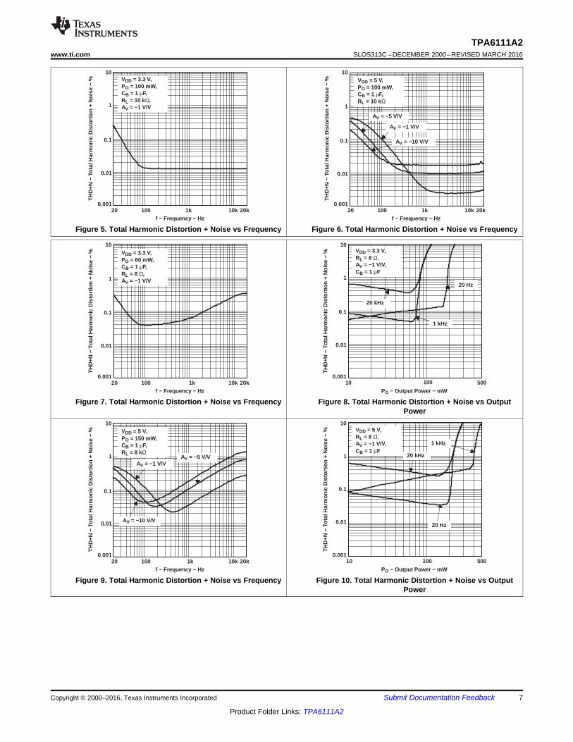
Figure 5. Total Harmonic Distortion + Noise vs Frequency Figure 6. Total Harmonic Distortion + Noise vs Frequency
Figure 7. Total Harmonic Distortion + Noise vs Frequency Figure 8. Total Harmonic Distortion + Noise vs OutputPower
Figure 9. Total Harmonic Distortion + Noise vs Frequency Figure 10. Total Harmonic Distortion + Noise vs OutputPower

−120
0
−110
−100
−90
−80
−70
−60
−50
−40
−30
−20
−10
20 20k100 1k 10kf − Frequency − Hz
VDD = 3.3 V,RL = 16 Ω,AV = −1 V/V
0.1 µF
− S
uppl
y R
ippl
e R
ejec
tion
Rat
io −
dB
0.47 µF
1 µF
KS
VR
Bypass = 1.65 V
− S
uppl
y R
ippl
e R
ejec
tion
Rat
io −
dB
KS
VR
−120
0
−110
−100
−90
−80
−70
−60
−50
−40
−30
−20
−10
20 20k100 1k 10kf − Frequency − Hz
VDD = 5 V,RL = 16 Ω,AV = −1 V/V
0.1 µF
Bypass = 2.5 V
1 µF
0.47 µF
20 20k100 1k 10k0.001
10
0.01
0.1
1
TH
D+N
− T
otal
Har
mon
ic D
isto
rtion
+ N
oise
− %
f − Frequency − Hz
VDD = 5 V,PO = 100 mW,CB = 1 µF,RL = 16 Ω
AV = −10 V/V
AV = −1 V/VAV = −5 V/V
10 500 0.001
10
0.01
0.1
1
TH
D+N
− T
otal
Har
mon
ic D
isto
rtion
+ N
oise
− %
VDD = 5 V,RL = 16 Ω,AV = −1 V/V,CB = 1 µF
PO − Output Power − mW
1 kHz
20 Hz
20 kHz
100
20 20k100 1k 10k0.001
10
0.01
0.1
1
TH
D+N
− T
otal
Har
mon
ic D
isto
rtion
+ N
oise
− %
f − Frequency − Hz
VDD = 3.3 V,PO = 40 mW,CB = 1 µF,RL = 16 Ω,AV = −1 V/V
10 500 0.001
10
0.01
0.1
1
TH
D+N
− T
otal
Har
mon
ic D
isto
rtion
+ N
oise
− %
VDD = 3.3 V,RL =16 Ω,AV = −1 V/V,CB = 1 µF
PO − Output Power − mW
1 kHz
20 kHz
100
20 Hz
8
TPA6111A2SLOS313C –DECEMBER 2000–REVISED MARCH 2016 www.ti.com
Product Folder Links: TPA6111A2
Submit Documentation Feedback Copyright © 2000–2016, Texas Instruments Incorporated
Figure 11. Total Harmonic Distortion + Noise vs Frequency Figure 12. Total Harmonic Distortion + Noise vs OutputPower
Figure 13. Total Harmonic Distortion + Noise vs Frequency Figure 14. Total Harmonic Distortion + Noise vs OutputPower
Figure 15. Supply Ripple Rejection Ratio vs Frequency Figure 16. Supply Ripple Rejection Ratio vs Frequency

−120
0
−110
−100
−90
−80
−70
−60
−50
−40
−30
−20
−10
20 20k100 1k 10kf − Frequency − Hz
Cro
ssta
lk −
dB
IN1− to VO2
IN2− to VO1
VDD = 3.3 V,PO = 60 mW,CB = 1 µF,RL = 8 Ω,AV = −1 V/V
−120
0
−110
−100
−90
−80
−70
−60
−50
−40
−30
−20
−10
20 20k100 1k 10kf − Frequency − Hz
Cro
ssta
lk −
dB
VDD = 5 V,PO = 60 mW,CB = 1 µF,RL = 32 Ω,AV = −1 V/V
IN1− to VO2
IN2− to VO1
−120
0
−110
−100
−90
−80
−70
−60
−50
−40
−30
−20
−10
20 20k100 1k 10kf − Frequency − Hz
Cro
ssta
lk −
dB
IN1− to VO2
IN2− to VO1
VDD = 3.3 V,PO = 25 mW,CB = 1 µF,RL = 32 Ω,AV = −1 V/V
−120
0
−110
−100
−90
−80
−70
−60
−50
−40
−30
−20
−10
20 20k100 1k 10kf − Frequency − Hz
Cro
ssta
lk −
dB
IN1− to VO2
IN2− to VO1
VDD = 3.3 V,PO = 40 mW,CB = 1 µF,RL = 16 Ω,AV = −1 V/V
100
10
120 20k100 1k 10k
f − Frequency − Hz
VDD = 3.3 V,BW = 10 Hz to 22 kHzRL = 16 Ω
− O
utpu
t Noi
se V
olta
ge −
V
nV
µ
AV = −1 V/V
AV = −10 V/V(R
MS
)
100
10
120 20k100 1k 10k
f − Frequency − Hz
VDD = 5 V,BW = 10 Hz to 22 kHzRL = 16 Ω,
AV = −1 V/V
AV = −10 V/V
− O
utpu
t Noi
se V
olta
ge −
V
nV
µ(R
MS
)
9
TPA6111A2www.ti.com SLOS313C –DECEMBER 2000–REVISED MARCH 2016
Product Folder Links: TPA6111A2
Submit Documentation FeedbackCopyright © 2000–2016, Texas Instruments Incorporated
Figure 17. Output Noise Voltage vs Frequency Figure 18. Output Noise Voltage vs Frequency
Figure 19. Crosstalk vs Frequency Figure 20. Crosstalk vs Frequency
Figure 21. Crosstalk vs Frequency Figure 22. Crosstalk vs Frequency

−40
−20
0
20
40
60
80
100
120
Ope
n-Lo
op G
ain
− dB
− P
hase
Mar
gin
− D
eg
1 k 10 k 100 k 1 M 10 M−180
−150
−120
−90
−60
−30
0
30
60
90
120
150
180
f − Frequency − Hz
Phase
Gain
VDD = 3.3 VRL = 10 kΩ
Φm
−40
−20
0
20
40
60
80
100
120
1 k 10 k 100 k 1 M 10 M−180
−150
−120
−90
−60
−30
0
30
60
90
120
150
180
Ope
n-Lo
op G
ain
− dB
f − Frequency − Hz
Phase
Gain
VDD = 5 VRL = 10 kΩ
− P
hase
Mar
gin
− D
egΦ
m
−100
−90
−80
−70
−60
−50
−40
−30
−20
−10
0
10 100 1 k 10 k 1 M
Shu
tdow
n A
ttenu
atio
n −
dB
f − Frequency − Hz
VDD = 3.3 V,RL = 16 Ω,CB = 1 µF
−100
−90
−80
−70
−60
−50
−40
−30
−20
−10
0
10 100 1 k 10 k 1 M
Shu
tdow
n A
ttenu
atio
n −
dB
f − Frequency − Hz
VDD = 5 V,RL = 16 Ω,CB = 1 µF
−120
0
−110
−100
−90
−80
−70
−60
−50
−40
−30
−20
−10
20 20k100 1k 10kf − Frequency − Hz
Cro
ssta
lk −
dB
VDD = 5 V,PO = 100 mW,CB = 1 µF,RL = 16 Ω,AV = −1 V/V
IN1− to VO2
IN2− to VO1
−120
0
−110
−100
−90
−80
−70
−60
−50
−40
−30
−20
−10
20 20k100 1k 10kf − Frequency − Hz
Cro
ssta
lk −
dB
VDD = 5 V,PO = 150 mW,CB = 1 µF,RL = 8 Ω,AV = −1 V/V
IN1− to VO2
IN2− to VO1
10
TPA6111A2SLOS313C –DECEMBER 2000–REVISED MARCH 2016 www.ti.com
Product Folder Links: TPA6111A2
Submit Documentation Feedback Copyright © 2000–2016, Texas Instruments Incorporated
Figure 23. Crosstalk vs Frequency Figure 24. Crosstalk vs Frequency
Figure 25. Shutdown Attenuation vs Frequency Figure 26. Shutdown Attenuation vs Frequency
Figure 27. Open-Loop Gain and Phase Margin vs Frequency Figure 28. Open-Loop Gain and Phase Margin vs Frequency

0
Pow
er D
issi
patio
n/A
mpl
ifier
− m
W
Load Power − mW
80
40
20
080 120 180 200
10
30
50
14010020 6040 160
60
70
VDD = 3.3 V8 Ω
16 Ω
64 Ω
32 Ω
0
Load Power − mW
180
100
60
080 120 180 200
40
80
120
14010020 6040 160
140
160 VDD = 5 V
8 Ω
16 Ω
64 Ω
32 Ω
20
Pow
er D
issi
patio
n/A
mpl
ifier
− m
W
0
20
40
60
80
100
120
1 2 3 4 5 6 7 8 9 10
SN
R −
Sig
nal-t
o-N
oise
Rat
io −
dB
AV − Voltage Gain − V/V
VDD = 5 V
0
0.5
1
1.5
2
2.5
0 0.5 1 1.5 2 2.5 3 3.5 4 4.5 5 5.5
− S
uppl
y C
urre
nt −
mA
I DD
VDD − Supply V oltage − V
50
25
08 12 16 20 32 36 40
75
100
45 52 56 64
− O
utpu
t Pow
er −
mW
RL − Load Resistance − Ω
VDD = 3.3 V,THD+N = 1%,AV = −1 V/V
24 28 44 60
P O
0
50
100
150
200
250
8 12 16 20 24 28 32 36 40 44 48 52 56 60 64
RL − Load Resistance − Ω
VDD = 5 V,THD+N = 1%,AV = −1 V/V
− O
utpu
t Pow
er −
mW
P O
11
TPA6111A2www.ti.com SLOS313C –DECEMBER 2000–REVISED MARCH 2016
Product Folder Links: TPA6111A2
Submit Documentation FeedbackCopyright © 2000–2016, Texas Instruments Incorporated
Figure 29. Output Power vs Load Resistance Figure 30. Output Power vs Load Resistance
Figure 31. Supply Current vs Supply Voltage Figure 32. Signal-to-Noise Ratio vs Voltage Gain
Figure 33. Power Dissipation and Amplifier vs Load Power Figure 34. Power Dissipation and Amplifier vs Load Power
8 Parameter Measurement Information
All parameters are measured according to the conditions described in the Specifications section.
Bias ControlBias Control
Left
Right
12
TPA6111A2SLOS313C –DECEMBER 2000–REVISED MARCH 2016 www.ti.com
Product Folder Links: TPA6111A2
Submit Documentation Feedback Copyright © 2000–2016, Texas Instruments Incorporated
9 Detailed Description
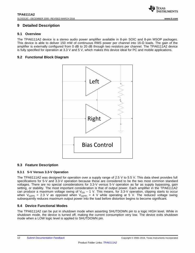
9.1 OverviewThe TPA6111A2 device is a stereo audio power amplifier available in 8-pin SOIC and 8-pin MSOP packages.This device is able to deliver 150 mW of continuous RMS power per channel into 16-Ω loads. The gain of theamplifier is externally configured from 0 dB to 20 dB through two resistors per channel. The TPA6111A2 deviceis fully specified for operation at 3.3 V and 5 V, which makes this device ideal for PC and mobile applications.
9.2 Functional Block Diagram
9.3 Feature Description
9.3.1 5-V Versus 3.3-V OperationThe TPA6111A2 was designed for operation over a supply range of 2.5 V to 5.5 V. This data sheet provides fullspecifications for 5-V and 3.3-V operation because these are considered to be the two most common standardvoltages. There are no special considerations for 3.3-V versus 5-V operation as far as supply bypassing, gainsetting, or stability. The most important consideration is that of output power. Each amplifier in the TPA6111A2can produce a maximum voltage swing of VDD – 1 V. This means, for 3.3-V operation, clipping starts to occurwhen VO(PP) = 2.3 V as opposed when VO(PP) = 4 V while operating at 5 V. The reduced voltage swingsubsequently reduces maximum output power into the load before distortion begins to become significant.
9.4 Device Functional ModesThe TPA6111A2 can be put in shutdown mode when asserting SHUTDOWN pin to a logic HIGH level. While inshutdown mode, the device is turned off, making the current consumption very low. The device exits shutdownmode when a LOW logic level is applied to SHUTDOWN pin.

AudioInput
BiasControl
8
1
7
4
VO1
VO2
VDD
5
2
3
6
IN1−
BYPASS
SHUTDOWN
VDD/2
CI
RI
RF
C(BYP)
C(S)
AudioInput
CI
RI IN2−
RF
VDD
From ShutdownControl Circuit
−+
−+
C(C)
C(C)
13
TPA6111A2www.ti.com SLOS313C –DECEMBER 2000–REVISED MARCH 2016
Product Folder Links: TPA6111A2
Submit Documentation FeedbackCopyright © 2000–2016, Texas Instruments Incorporated
10 Application and Implementation
NOTEInformation in the following applications sections is not part of the TI componentspecification, and TI does not warrant its accuracy or completeness. TI’s customers areresponsible for determining suitability of components for their purposes. Customers shouldvalidate and test their design implementation to confirm system functionality.
10.1 Application InformationThis typical connection diagram highlights the required external components and system level connections forproper operation of the device in popular use case. Any design variation can be supported by TI throughschematic and layout reviews. Visit http://e2e.ti.com for design assistance and join the audio amplifier discussionforum for additional information.
10.2 Typical Application
Figure 35. Typical Application
10.2.1 Design RequirementsTable 2 lists the design requirements of the TPA111A2.
Table 2. Design RequirementsDESIGN PARAMETER EXAMPLE VALUE
Input voltage supply range 3.3 V to 5 VCurrent 2 mA
Load impedance 16 Ω
II c highpass
CR f ( )
1
2=
p
c highpassI I
fR C
( )
1
2=
p
c lowpassF F
fR C
( )
1
2=
p
F I
F I
R REffective Impedance =
R R
æ ö- ç ÷
+è ø
F
I
RGain =
R
æ ö- ç ÷
è ø
14
TPA6111A2SLOS313C –DECEMBER 2000–REVISED MARCH 2016 www.ti.com
Product Folder Links: TPA6111A2
Submit Documentation Feedback Copyright © 2000–2016, Texas Instruments Incorporated
10.2.2 Detailed Design Procedure
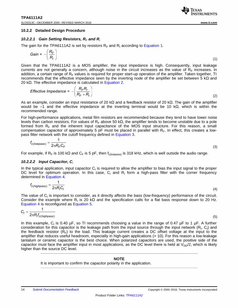
10.2.2.1 Gain Setting Resistors, RF and Ri
The gain for the TPA6111A2 is set by resistors RF and RI according to Equation 1.
(1)
Given that the TPA6111A2 is a MOS amplifier, the input impedance is high. Consequently, input leakagecurrents are not generally a concern, although noise in the circuit increases as the value of RF increases. Inaddition, a certain range of RF values is required for proper start-up operation of the amplifier. Taken together, TIrecommends that the effective impedance seen by the inverting node of the amplifier be set between 5 kΩ and20 kΩ. The effective impedance is calculated in Equation 2.
(2)
As an example, consider an input resistance of 20 kΩ and a feedback resistor of 20 kΩ. The gain of the amplifierwould be –1 and the effective impedance at the inverting terminal would be 10 kΩ, which is within therecommended range.
For high-performance applications, metal film resistors are recommended because they tend to have lower noiselevels than carbon resistors. For values of RF above 50 kΩ, the amplifier tends to become unstable due to a poleformed from RF and the inherent input capacitance of the MOS input structure. For this reason, a smallcompensation capacitor of approximately 5 pF must be placed in parallel with RF. In effect, this creates a low-pass filter network with the cutoff frequency defined in Equation 3.
(3)
For example, if RF is 100 kΩ and CF is 5 pF, then fc(lowpass) is 318 kHz, which is well outside the audio range.
10.2.2.2 Input Capacitor, Ci
In the typical application, input capacitor CI is required to allow the amplifier to bias the input signal to the properDC level for optimum operation. In this case, Ci and RI form a high-pass filter with the corner frequencydetermined in Equation 4.
(4)
The value of CI is important to consider, as it directly affects the bass (low-frequency) performance of the circuit.Consider the example where RI is 20 kΩ and the specification calls for a flat bass response down to 20 Hz.Equation 4 is reconfigured as Equation 5.
(5)
In this example, CI is 0.40 µF, so TI recommends choosing a value in the range of 0.47 µF to 1 µF. A furtherconsideration for this capacitor is the leakage path from the input source through the input network (RI, CI) andthe feedback resistor (RF) to the load. This leakage current creates a DC offset voltage at the input to theamplifier that reduces useful headroom, especially in high-gain applications (> 10). For this reason a low-leakagetantalum or ceramic capacitor is the best choice. When polarized capacitors are used, the positive side of thecapacitor must face the amplifier input in most applications, as the DC level there is held at VDD/2, which is likelyhigher than the source DC level.
NOTEIt is important to confirm the capacitor polarity in the application.
( ) I I L CBYPC R R CC 230 k ( )( )
1 1 1
( )£ £
´ W
c
L C
fR C( )
1
2=
p
( ) I IBYPC RC 230 kΩ( )
1 1
( )£
´
15
TPA6111A2www.ti.com SLOS313C –DECEMBER 2000–REVISED MARCH 2016
Product Folder Links: TPA6111A2
Submit Documentation FeedbackCopyright © 2000–2016, Texas Instruments Incorporated
10.2.2.3 Power Supply Decoupling, C(S)
The TPA6111A2 is a high-performance CMOS audio amplifier that requires adequate power supply decoupling toensure that the output total harmonic distortion (THD) is as low as possible. Power supply decoupling alsoprevents oscillations for long lead lengths between the amplifier and the speaker. The optimum decoupling isachieved by using two capacitors of different types that target different types of noise on the power supply leads.For higher frequency transients, spikes, or digital hash on the line, a good low equivalent-series-resistance (ESR)ceramic capacitor, typically 0.1 µF, placed as close as possible to the device VDD lead, works best. For filteringlower frequency noise signals, a larger aluminum electrolytic capacitor of 10 µF or greater placed near the poweramplifier is recommended.
10.2.2.4 Midrail Bypass Capacitor, C(BYP)
The midrail bypass capacitor, C(BYP), serves several important functions. During start-up, C(BYP) determines therate at which the amplifier starts up. This helps to push the start-up pop noise into the subaudible range (so low itcannot be heard). The second function is to reduce noise produced by the power supply caused by coupling intothe output drive signal. This noise is from the midrail generation circuit internal to the amplifier. The capacitor isfed from a 230-kΩ source inside the amplifier. To keep the start-up pop as low as possible, the relationshipshown in Equation 6 must be maintained.
(6)
As an example, consider a circuit where C(BYP) is 1 µF, CI is 1 µF, and RI is 20 kΩ. Inserting these values intoEquation 6 results in: 6.25 ≤ 50 which satisfies the rule. Recommended values for bypass capacitor C(BYP) are0.1-µF to 1-µF, ceramic or tantalum low-ESR, for the best THD and noise performance.
10.2.2.5 Output Coupling Capacitor, C(C)
In the typical single-supply single-ended (SE) configuration, an output coupling capacitor (CC) is required to blockthe DC bias at the output of the amplifier, thus preventing DC currents in the load. As with the input couplingcapacitor, the output coupling capacitor and impedance of the load form a high-pass filter governed byEquation 7.
(7)
The main disadvantage, from a performance standpoint, is that the typically small load impedances drive the low-frequency corner higher. Large values of C(C) are required to pass low frequencies into the load. Consider theexample where a C(C) of 68 µF is chosen and loads vary from 32 Ω to 47 kΩ. Table 3 summarizes the frequencyresponse characteristics of each configuration.
Table 3. Common Load Impedances vs Low FrequencyOutput Characteristics in SE Mode
RL CC LOWEST FREQUENCY32 Ω 68 µF 73 Hz
10,000 Ω 68 µF 0.23 Hz47,000 Ω 68 µF 0.05 Hz
As Table 3 indicates, headphone response is adequate and drive into line level inputs (a home stereo forexample) is good.
The output coupling capacitor required in single-supply SE mode also places additional constraints on theselection of other components in the amplifier circuit. With the rules described earlier still valid, add the followingrelationship in Equation 8:
(8)

16
TPA6111A2SLOS313C –DECEMBER 2000–REVISED MARCH 2016 www.ti.com
Product Folder Links: TPA6111A2
Submit Documentation Feedback Copyright © 2000–2016, Texas Instruments Incorporated
10.2.2.6 Using Low-ESR CapacitorsLow-ESR capacitors are recommended throughout this application. A real capacitor can be modeled simply as aresistor in series with an ideal capacitor. The voltage drop across this resistor minimizes the beneficial effects ofthe capacitor in the circuit. The lower the equivalent value of this resistance, the more the real capacitor behaveslike an ideal capacitor.
10.2.3 Application CurvesThe characteristics of this design are shown in Table 4 from the Typical Characteristics section.
Table 4. Table of GraphsFIGURE
THD+N Total harmonic distortion plus noisevs Frequency Figure 11vs Output power Figure 12
11 Power Supply RecommendationsThe device is designed to operate form an input voltage supply of 3.3 V and 5 V. Therefore, the output voltagerange of power supply must be within this range and well regulated. Ti recommends placing decouplingcapacitors in every voltage source pin. Place these decoupling capacitors as close as possible to theTPA6111A2.

SHUTDOWN
Vo2
Via to Ground Plane
Ground Plane Top Layer Traces
Pad to Ground Plane
Decoupling capacitor placed as close as
possible to the deviceTPA6111A2
Via to Power Supply
Thermal Pad
1234
85
Vo1IN1
IN2
6 7
17
TPA6111A2www.ti.com SLOS313C –DECEMBER 2000–REVISED MARCH 2016
Product Folder Links: TPA6111A2
Submit Documentation FeedbackCopyright © 2000–2016, Texas Instruments Incorporated
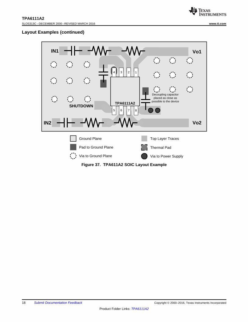
12 Layout
12.1 Layout GuidelinesSolder the exposed metal pad on the TPA6111A2 DGN package to the PCB. The pad on the PCB may begrounded or may be allowed to float (not be connected to ground or power). If the pad is grounded, it must beconnected to the same ground as the GND pin (4). See the layout and mechanical drawings in Mechanical,Packaging, and Orderable Information for proper sizing. Soldering the thermal pad improves mechanicalreliability, improves grounding of the device, and enhances thermal conductivity of the package.
12.2 Layout Examples
Figure 36. TPA611A2 MSOP Layout Example
SHUTDOWN
Vo2
Via to Ground Plane
Ground Plane Top Layer Traces
Pad to Ground Plane
Decoupling capacitor placed as close as
possible to the deviceTPA6111A2
Via to Power Supply
Thermal Pad
1234
85
Vo1IN1
IN2
6 7
18
TPA6111A2SLOS313C –DECEMBER 2000–REVISED MARCH 2016 www.ti.com
Product Folder Links: TPA6111A2
Submit Documentation Feedback Copyright © 2000–2016, Texas Instruments Incorporated
Layout Examples (continued)
Figure 37. TPA611A2 SOIC Layout Example

19
TPA6111A2www.ti.com SLOS313C –DECEMBER 2000–REVISED MARCH 2016
Product Folder Links: TPA6111A2
Submit Documentation FeedbackCopyright © 2000–2016, Texas Instruments Incorporated
13 Device and Documentation Support
13.1 Documentation Support
13.1.1 Related DocumentationFor related documentation, see the following:
PowerPAD Thermally Enhanced Package Application Report (SLMA002)
13.2 Community ResourcesThe following links connect to TI community resources. Linked contents are provided "AS IS" by the respectivecontributors. They do not constitute TI specifications and do not necessarily reflect TI's views; see TI's Terms ofUse.
TI E2E™ Online Community TI's Engineer-to-Engineer (E2E) Community. Created to foster collaborationamong engineers. At e2e.ti.com, you can ask questions, share knowledge, explore ideas and helpsolve problems with fellow engineers.
Design Support TI's Design Support Quickly find helpful E2E forums along with design support tools andcontact information for technical support.
13.3 TrademarksPowerPAD, E2E are trademarks of Texas Instruments.All other trademarks are the property of their respective owners.
13.4 Electrostatic Discharge CautionThese devices have limited built-in ESD protection. The leads should be shorted together or the device placed in conductive foamduring storage or handling to prevent electrostatic damage to the MOS gates.
13.5 GlossarySLYZ022 — TI Glossary.
This glossary lists and explains terms, acronyms, and definitions.
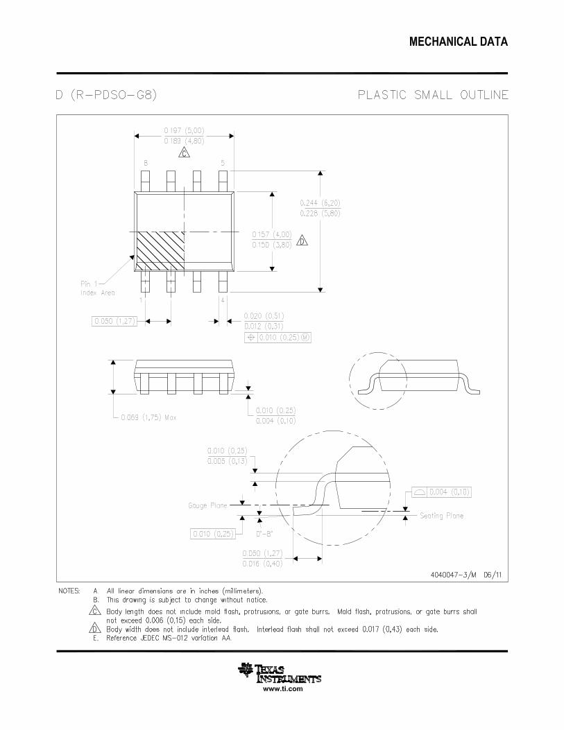
14 Mechanical, Packaging, and Orderable InformationThe following pages include mechanical, packaging, and orderable information. This information is the mostcurrent data available for the designated devices. This data is subject to change without notice and revision ofthis document. For browser-based versions of this data sheet, refer to the left-hand navigation.
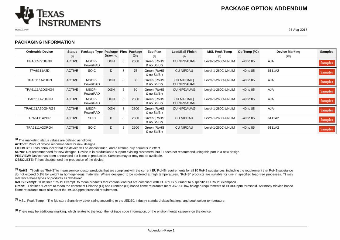
PACKAGE OPTION ADDENDUM
www.ti.com 24-Aug-2018
Addendum-Page 1
PACKAGING INFORMATION
Orderable Device Status(1)
Package Type PackageDrawing
Pins PackageQty
Eco Plan(2)
Lead/Ball Finish(6)
MSL Peak Temp(3)
Op Temp (°C) Device Marking(4/5)
Samples
HPA00577DGNR ACTIVE MSOP-PowerPAD
DGN 8 2500 Green (RoHS& no Sb/Br)
CU NIPDAUAG Level-1-260C-UNLIM -40 to 85 AJA
TPA6111A2D ACTIVE SOIC D 8 75 Green (RoHS& no Sb/Br)
CU NIPDAU Level-1-260C-UNLIM -40 to 85 6111A2
TPA6111A2DGN ACTIVE MSOP-PowerPAD
DGN 8 80 Green (RoHS& no Sb/Br)
CU NIPDAU |CU NIPDAUAG
Level-1-260C-UNLIM -40 to 85 AJA
TPA6111A2DGNG4 ACTIVE MSOP-PowerPAD
DGN 8 80 Green (RoHS& no Sb/Br)
CU NIPDAUAG Level-1-260C-UNLIM -40 to 85 AJA
TPA6111A2DGNR ACTIVE MSOP-PowerPAD
DGN 8 2500 Green (RoHS& no Sb/Br)
CU NIPDAU |CU NIPDAUAG
Level-1-260C-UNLIM -40 to 85 AJA
TPA6111A2DGNRG4 ACTIVE MSOP-PowerPAD
DGN 8 2500 Green (RoHS& no Sb/Br)
CU NIPDAUAG Level-1-260C-UNLIM -40 to 85 AJA
TPA6111A2DR ACTIVE SOIC D 8 2500 Green (RoHS& no Sb/Br)
CU NIPDAU Level-1-260C-UNLIM -40 to 85 6111A2
TPA6111A2DRG4 ACTIVE SOIC D 8 2500 Green (RoHS& no Sb/Br)
CU NIPDAU Level-1-260C-UNLIM -40 to 85 6111A2
(1) The marketing status values are defined as follows:ACTIVE: Product device recommended for new designs.LIFEBUY: TI has announced that the device will be discontinued, and a lifetime-buy period is in effect.NRND: Not recommended for new designs. Device is in production to support existing customers, but TI does not recommend using this part in a new design.PREVIEW: Device has been announced but is not in production. Samples may or may not be available.OBSOLETE: TI has discontinued the production of the device.
(2) RoHS: TI defines "RoHS" to mean semiconductor products that are compliant with the current EU RoHS requirements for all 10 RoHS substances, including the requirement that RoHS substancedo not exceed 0.1% by weight in homogeneous materials. Where designed to be soldered at high temperatures, "RoHS" products are suitable for use in specified lead-free processes. TI mayreference these types of products as "Pb-Free".RoHS Exempt: TI defines "RoHS Exempt" to mean products that contain lead but are compliant with EU RoHS pursuant to a specific EU RoHS exemption.Green: TI defines "Green" to mean the content of Chlorine (Cl) and Bromine (Br) based flame retardants meet JS709B low halogen requirements of <=1000ppm threshold. Antimony trioxide basedflame retardants must also meet the <=1000ppm threshold requirement.
(3) MSL, Peak Temp. - The Moisture Sensitivity Level rating according to the JEDEC industry standard classifications, and peak solder temperature.
(4) There may be additional marking, which relates to the logo, the lot trace code information, or the environmental category on the device.

PACKAGE OPTION ADDENDUM
www.ti.com 24-Aug-2018
Addendum-Page 2
(5) Multiple Device Markings will be inside parentheses. Only one Device Marking contained in parentheses and separated by a "~" will appear on a device. If a line is indented then it is a continuationof the previous line and the two combined represent the entire Device Marking for that device.
(6) Lead/Ball Finish - Orderable Devices may have multiple material finish options. Finish options are separated by a vertical ruled line. Lead/Ball Finish values may wrap to two lines if the finishvalue exceeds the maximum column width.
Important Information and Disclaimer:The information provided on this page represents TI's knowledge and belief as of the date that it is provided. TI bases its knowledge and belief on informationprovided by third parties, and makes no representation or warranty as to the accuracy of such information. Efforts are underway to better integrate information from third parties. TI has taken andcontinues to take reasonable steps to provide representative and accurate information but may not have conducted destructive testing or chemical analysis on incoming materials and chemicals.TI and TI suppliers consider certain information to be proprietary, and thus CAS numbers and other limited information may not be available for release.
In no event shall TI's liability arising out of such information exceed the total purchase price of the TI part(s) at issue in this document sold by TI to Customer on an annual basis.

TAPE AND REEL INFORMATION
*All dimensions are nominal
Device PackageType
PackageDrawing
Pins SPQ ReelDiameter
(mm)
ReelWidth
W1 (mm)
A0(mm)
B0(mm)
K0(mm)
P1(mm)
W(mm)
Pin1Quadrant
TPA6111A2DGNR MSOP-Power PAD
DGN 8 2500 330.0 12.4 5.3 3.4 1.4 8.0 12.0 Q1
TPA6111A2DGNR MSOP-Power PAD
DGN 8 2500 330.0 12.4 5.3 3.4 1.4 8.0 12.0 Q1
TPA6111A2DR SOIC D 8 2500 330.0 12.4 6.4 5.2 2.1 8.0 12.0 Q1
PACKAGE MATERIALS INFORMATION
www.ti.com 3-Aug-2017
Pack Materials-Page 1

*All dimensions are nominal
Device Package Type Package Drawing Pins SPQ Length (mm) Width (mm) Height (mm)
TPA6111A2DGNR MSOP-PowerPAD DGN 8 2500 364.0 364.0 27.0
TPA6111A2DGNR MSOP-PowerPAD DGN 8 2500 358.0 335.0 35.0
TPA6111A2DR SOIC D 8 2500 340.5 338.1 20.6
PACKAGE MATERIALS INFORMATION
www.ti.com 3-Aug-2017
Pack Materials-Page 2


IMPORTANT NOTICE
Texas Instruments Incorporated (TI) reserves the right to make corrections, enhancements, improvements and other changes to itssemiconductor products and services per JESD46, latest issue, and to discontinue any product or service per JESD48, latest issue. Buyersshould obtain the latest relevant information before placing orders and should verify that such information is current and complete.TI’s published terms of sale for semiconductor products (http://www.ti.com/sc/docs/stdterms.htm) apply to the sale of packaged integratedcircuit products that TI has qualified and released to market. Additional terms may apply to the use or sale of other types of TI products andservices.Reproduction of significant portions of TI information in TI data sheets is permissible only if reproduction is without alteration and isaccompanied by all associated warranties, conditions, limitations, and notices. TI is not responsible or liable for such reproduceddocumentation. Information of third parties may be subject to additional restrictions. Resale of TI products or services with statementsdifferent from or beyond the parameters stated by TI for that product or service voids all express and any implied warranties for theassociated TI product or service and is an unfair and deceptive business practice. TI is not responsible or liable for any such statements.Buyers and others who are developing systems that incorporate TI products (collectively, “Designers”) understand and agree that Designersremain responsible for using their independent analysis, evaluation and judgment in designing their applications and that Designers havefull and exclusive responsibility to assure the safety of Designers' applications and compliance of their applications (and of all TI productsused in or for Designers’ applications) with all applicable regulations, laws and other applicable requirements. Designer represents that, withrespect to their applications, Designer has all the necessary expertise to create and implement safeguards that (1) anticipate dangerousconsequences of failures, (2) monitor failures and their consequences, and (3) lessen the likelihood of failures that might cause harm andtake appropriate actions. Designer agrees that prior to using or distributing any applications that include TI products, Designer willthoroughly test such applications and the functionality of such TI products as used in such applications.TI’s provision of technical, application or other design advice, quality characterization, reliability data or other services or information,including, but not limited to, reference designs and materials relating to evaluation modules, (collectively, “TI Resources”) are intended toassist designers who are developing applications that incorporate TI products; by downloading, accessing or using TI Resources in anyway, Designer (individually or, if Designer is acting on behalf of a company, Designer’s company) agrees to use any particular TI Resourcesolely for this purpose and subject to the terms of this Notice.TI’s provision of TI Resources does not expand or otherwise alter TI’s applicable published warranties or warranty disclaimers for TIproducts, and no additional obligations or liabilities arise from TI providing such TI Resources. TI reserves the right to make corrections,enhancements, improvements and other changes to its TI Resources. TI has not conducted any testing other than that specificallydescribed in the published documentation for a particular TI Resource.Designer is authorized to use, copy and modify any individual TI Resource only in connection with the development of applications thatinclude the TI product(s) identified in such TI Resource. NO OTHER LICENSE, EXPRESS OR IMPLIED, BY ESTOPPEL OR OTHERWISETO ANY OTHER TI INTELLECTUAL PROPERTY RIGHT, AND NO LICENSE TO ANY TECHNOLOGY OR INTELLECTUAL PROPERTYRIGHT OF TI OR ANY THIRD PARTY IS GRANTED HEREIN, including but not limited to any patent right, copyright, mask work right, orother intellectual property right relating to any combination, machine, or process in which TI products or services are used. Informationregarding or referencing third-party products or services does not constitute a license to use such products or services, or a warranty orendorsement thereof. Use of TI Resources may require a license from a third party under the patents or other intellectual property of thethird party, or a license from TI under the patents or other intellectual property of TI.TI RESOURCES ARE PROVIDED “AS IS” AND WITH ALL FAULTS. TI DISCLAIMS ALL OTHER WARRANTIES ORREPRESENTATIONS, EXPRESS OR IMPLIED, REGARDING RESOURCES OR USE THEREOF, INCLUDING BUT NOT LIMITED TOACCURACY OR COMPLETENESS, TITLE, ANY EPIDEMIC FAILURE WARRANTY AND ANY IMPLIED WARRANTIES OFMERCHANTABILITY, FITNESS FOR A PARTICULAR PURPOSE, AND NON-INFRINGEMENT OF ANY THIRD PARTY INTELLECTUALPROPERTY RIGHTS. TI SHALL NOT BE LIABLE FOR AND SHALL NOT DEFEND OR INDEMNIFY DESIGNER AGAINST ANY CLAIM,INCLUDING BUT NOT LIMITED TO ANY INFRINGEMENT CLAIM THAT RELATES TO OR IS BASED ON ANY COMBINATION OFPRODUCTS EVEN IF DESCRIBED IN TI RESOURCES OR OTHERWISE. IN NO EVENT SHALL TI BE LIABLE FOR ANY ACTUAL,DIRECT, SPECIAL, COLLATERAL, INDIRECT, PUNITIVE, INCIDENTAL, CONSEQUENTIAL OR EXEMPLARY DAMAGES INCONNECTION WITH OR ARISING OUT OF TI RESOURCES OR USE THEREOF, AND REGARDLESS OF WHETHER TI HAS BEENADVISED OF THE POSSIBILITY OF SUCH DAMAGES.Unless TI has explicitly designated an individual product as meeting the requirements of a particular industry standard (e.g., ISO/TS 16949and ISO 26262), TI is not responsible for any failure to meet such industry standard requirements.Where TI specifically promotes products as facilitating functional safety or as compliant with industry functional safety standards, suchproducts are intended to help enable customers to design and create their own applications that meet applicable functional safety standardsand requirements. Using products in an application does not by itself establish any safety features in the application. Designers mustensure compliance with safety-related requirements and standards applicable to their applications. Designer may not use any TI products inlife-critical medical equipment unless authorized officers of the parties have executed a special contract specifically governing such use.Life-critical medical equipment is medical equipment where failure of such equipment would cause serious bodily injury or death (e.g., lifesupport, pacemakers, defibrillators, heart pumps, neurostimulators, and implantables). Such equipment includes, without limitation, allmedical devices identified by the U.S. Food and Drug Administration as Class III devices and equivalent classifications outside the U.S.TI may expressly designate certain products as completing a particular qualification (e.g., Q100, Military Grade, or Enhanced Product).Designers agree that it has the necessary expertise to select the product with the appropriate qualification designation for their applicationsand that proper product selection is at Designers’ own risk. Designers are solely responsible for compliance with all legal and regulatoryrequirements in connection with such selection.Designer will fully indemnify TI and its representatives against any damages, costs, losses, and/or liabilities arising out of Designer’s non-compliance with the terms and provisions of this Notice.
Mailing Address: Texas Instruments, Post Office Box 655303, Dallas, Texas 75265Copyright © 2018, Texas Instruments Incorporated