tool cleanliness characterization for improving...
TRANSCRIPT
Tool Cleanliness Tool Cleanliness Characterization for Improving Characterization for Improving
Productivity and YieldsProductivity and Yields
Victor K.F. Chia, [email protected]
Victor K.F. Chia, [email protected]
Reducing Contamination
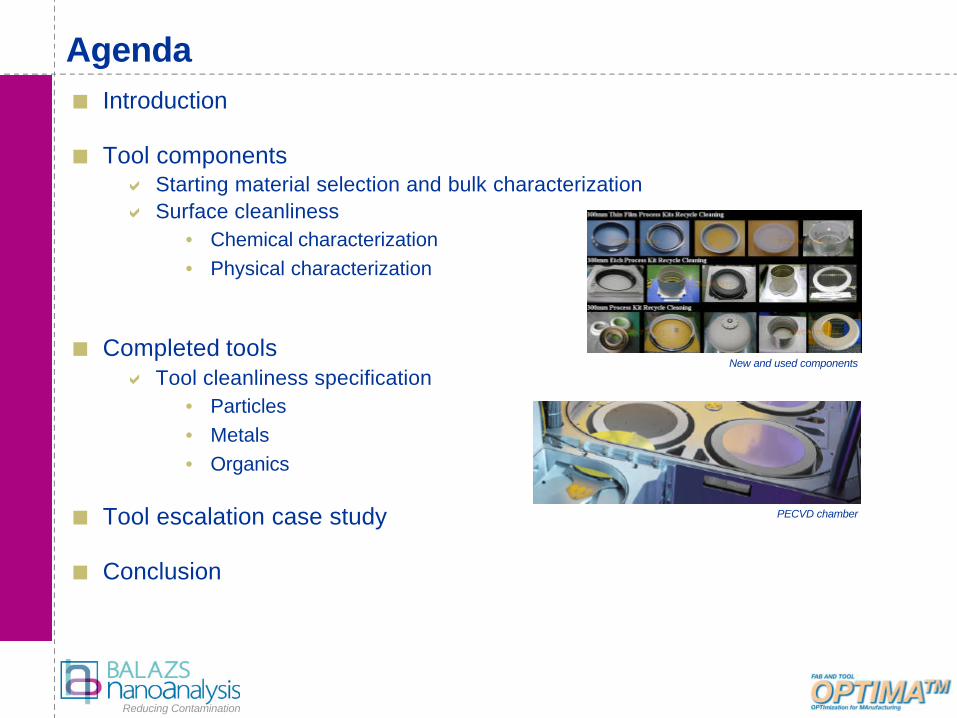
Agenda¢ Introduction
¢ Tool componentsa Starting material selection and bulk characterizationa Surface cleanliness
• Chemical characterization • Physical characterization
¢ Completed toolsa Tool cleanliness specification
• Particles• Metals• Organics
¢ Tool escalation case study
¢ Conclusion
New and used components
PECVD chamber

Reducing Contamination
Introduction¢ Tool parts cleanliness is an invisible parameter that must be controlled to
enable clean processing ¢ The target contaminants affecting process yields are particles, metals and
organics¢ In the sub-100 nm technology node even irreducible differences in the
components of identical tool chambers can influence yield and mean time between failure (MTBF)
¢ The first line of defense for a fab is to have clean tools for processing, from acceptance trials of the new tool to after each PM. Only with clean tools can a fab maximize its yield by increasing overall equipment productivity and wafer throughput for increased profit margin
¢ This may be accomplished with strict quality control of the supplier chain for starting materials, machine shops, cleaning vendors and contractmanufacturing. In addition, cleanliness specifications must be in place for the BOM.
¢ This presentation reviews cleanliness specifications for components and completed tools and characterization methods for verifying their cleanliness
Reducing Contamination
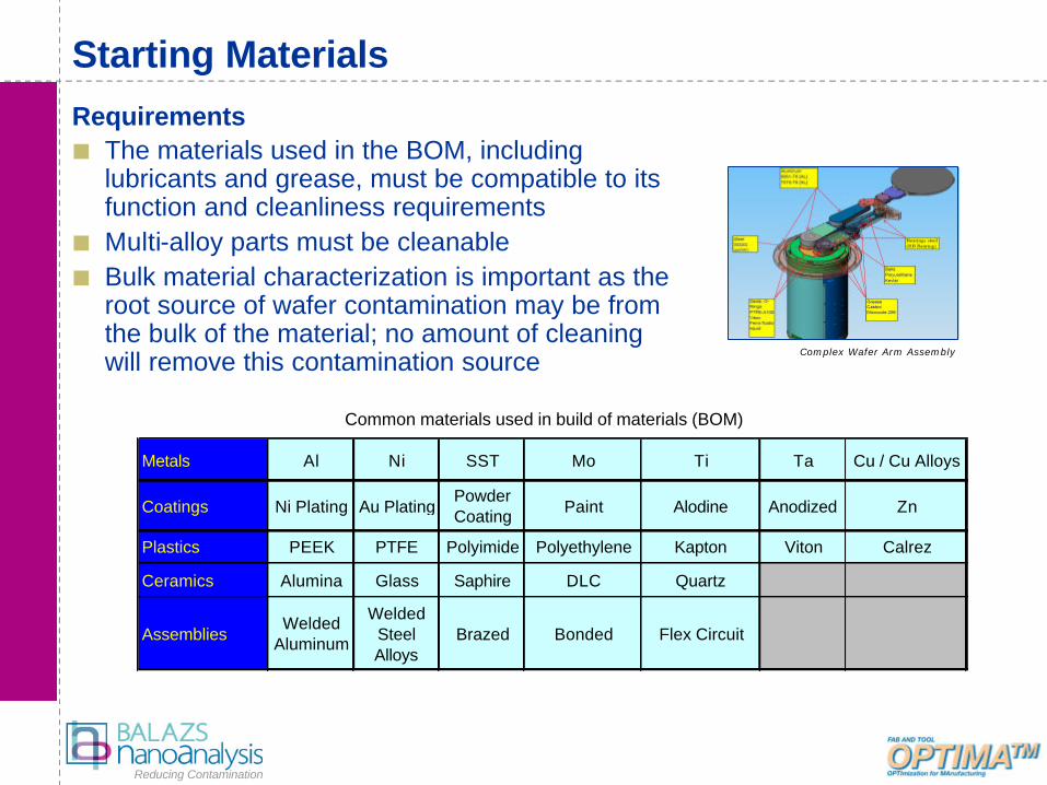
Starting MaterialsRequirements¢ The materials used in the BOM, including
lubricants and grease, must be compatible to its function and cleanliness requirements
¢ Multi-alloy parts must be cleanable¢ Bulk material characterization is important as the
root source of wafer contamination may be from the bulk of the material; no amount of cleaning will remove this contamination source
Metals Al Ni SST Mo Ti Ta Cu / Cu Alloys
Coatings Ni Plating Au Plating Powder Coating Paint Alodine Anodized Zn
Plastics PEEK PTFE Polyimide Polyethylene Kapton Viton Calrez
Ceramics Alumina Glass Saphire DLC Quartz
AssembliesWelded
Aluminum
Welded Steel Alloys
Brazed Bonded Flex Circuit
Complex Wafer Arm Assembly
Common materials used in build of materials (BOM)

Reducing Contamination
Starting Materials Characterization
¢ O-rings with inorganic fillers like SiO2, BaSO4, ZnO, C or TiO2 lasts about 6,000 wafer counts before particulation issues occurs
¢ O-rings using organic filled material can reach upwards of 20,000 wafer counts with reduced number of metallic particles escalations
Layer 1
Layer 4
Substrate
Layer 2
Layer 3
80E80E80E80E
Mass Spectrum
0
100000
200000
300000
400000
500000
0 20 40 60 80 100 120 140 160 180 200m/z (amu)
Sig
nal
Inte
nsi
ty (
c/s)
O-Ring Defect
S
Fe
Mn
I
C
Ni Mo
Metals on wafer using VPD ICP-MC
Mass Spectrum
0
20000
40000
60000
80000
100000
0 10 20 30 40 50 60 70 80m/z (amu)
Sig
nal Int
ensity
(c/s
)
Defect Inclusionthat is only visible under UV light
Si
OX
Y
Quartz
Si
O XY
100
1000
10000
100000
-1 0 1 2 3 4
Sampling Depth in µm
ICP
-MS
Sig
nal
Inte
nsi
ty (c
/s)
Iron (Fe)
Copper (Cu)
Zinc (Zn)
wafer
Fe
Cu
Zn
Fe
“clean”
“dirty”Ceramic
Metal or metal alloy whose melting temperature is considerably lower than the sintering temperature of the ceramic body are used to fill voids in the ceramic to achieve a particular physical property –conduction, brazing, etc.
Laser ablation ICP-MS
wafer
O-Ring
O-ring defect
FeMoS
I
Reducing Contamination
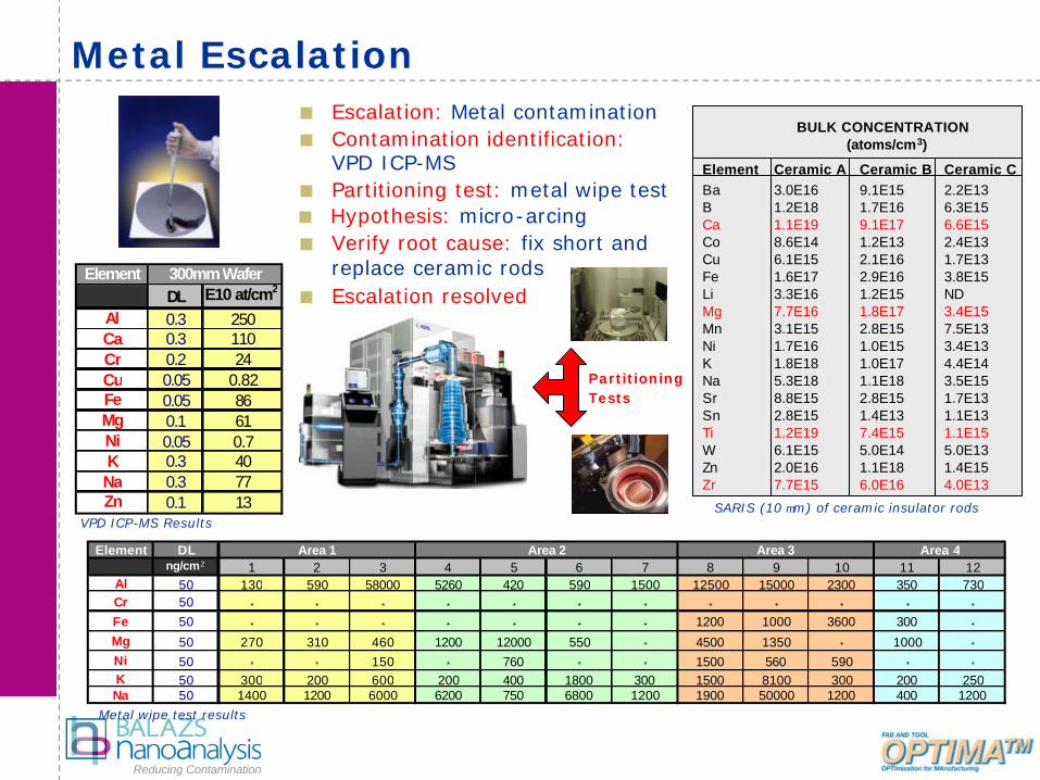
Metal Escalation¢ Escalation: Metal contamination
¢ Verify root cause: fix short and replace ceramic rods
¢ Escalation resolved
Element DL1 2 3 4 5 6 7 8 9 10 11 12
Al 50 130 590 58000 5260 420 590 1500 12500 15000 2300 350 730Cr 50 * * * * * * * * * * * *
Fe 50 * * * * * * * 1200 1000 3600 300 *
Mg 50 270 310 460 1200 12000 550 * 4500 1350 * 1000 *
Ni 50 * * 150 * 760 * * 1500 560 590 * *
K 50 300 200 600 200 400 1800 300 1500 8100 300 200 250Na 50 1400 1200 6000 6200 750 6800 1200 1900 50000 1200 400 1200
Area 1 Area 2 Area 3 Area 4
Metal wipe test results
ng/cm2
¢ Contamination identification:VPD ICP-MS
ElementDL E10 at/cm2
Al 0.3 250Ca 0.3 110Cr 0.2 24Cu 0.05 0.82Fe 0.05 86Mg 0.1 61Ni 0.05 0.7K 0.3 40Na 0.3 77Zn 0.1 13
300mm Wafer
VPD ICP-MS Results
BULK CONCENTRATION(atoms/cm3)
Element Ceramic A Ceramic B Ceramic CBa 3.0E16 9.1E15 2.2E13B 1.2E18 1.7E16 6.3E15Ca 1.1E19 9.1E17 6.6E15Co 8.6E14 1.2E13 2.4E13Cu 6.1E15 2.1E16 1.7E13Fe 1.6E17 2.9E16 3.8E15Li 3.3E16 1.2E15 NDMg 7.7E16 1.8E17 3.4E15Mn 3.1E15 2.8E15 7.5E13Ni 1.7E16 1.0E15 3.4E13K 1.8E18 1.0E17 4.4E14Na 5.3E18 1.1E18 3.5E15Sr 8.8E15 2.8E15 1.7E13Sn 2.8E15 1.4E13 1.1E13Ti 1.2E19 7.4E15 1.1E15W 6.1E15 5.0E14 5.0E13Zn 2.0E16 1.1E18 1.4E15Zr 7.7E15 6.0E16 4.0E13
SARIS (10 µm) of ceramic insulator rods
Partitioning Tests
¢ Partitioning test: metal wipe test¢ Hypothesis: micro-arcing

Reducing Contamination
Starting Materials Characterization
RED: material that may outgas
Part Description Material/Composition
Cable CoaxialConductor Material: Silver Plated Copper Covered Steel (SPCCS); Insulation Material: Tetrafluoroethylene (TFE); Outer Shield Material: Silver Plated Copper; Outer Jacket Material: Fluorinated Ethylene Propoylene
Connector for Coaxial PlugShell: Brass; Plug Body: Brass; Cable Clamp, Inner Sleeve, Washer or Nuts: Brass; Male Crimp Contacts: Bronze; Female Crimp Contacts: Bronze
Connector for Coaxial Plug - 50 Ohm
Outer Shell: Brass, Stainless Steel, Aluminum Alloy, PEEK; Sealing Resin: Epoxy; Grounding Crown: Bronze, Beryllium Copper, Stainless Steel; Latch Sleeve: Special Brass, Stainless Steel; Locking Washer: Bronze; Hexagonal or Round Nut: Brass, Stainless Steel, Aluminium alloy; Other Metallic Components: Brass, Stainless Steel; O-Ring and Gaskets: Silicone
Cable CoaxialConductor Material: Silver Plated Copper Covered Steel; Insulation Material: Tetrafluoroethylene (TFE); Outer Shield Material: Silver Plated Copper Covered Steel; Outer Jacket Material: Fluorinated Ethylene Propylene
Connector Socket, Open End Contact Material: Copper Alloy; Contact Underplating: Nickel; Insulation Material: Glass Filled Polyester (PBT)
Sensor, Light/Dark Materials: Polybutylene Phthalate (PBT); Cover: Polycarbonate; Emitter: Polycarbonate
Wire, 28 AWG, Black * Conductor Material: Silver Plated Copper; Insulation Material: Tetrafluoroethylene (TFE)
Connector, Socket 26 Position, Open EndContact Material: Copper Alloy; Contact Underplating: Nickel; Insulation Material: Glass Filled Polyester (PBT)
Shrink Tubing, 3/32 ID, Kyanr, Clear Polyvinylidene Fluoride
Wire, 28 AWG, Black * Conductor Material - Silver Plated Copper, Insulation Material: Fluorinated Ethylene Propylene (FEP)
Cable, High Voltage, 22 AWG, Stranded Silver Plated Conductor, Overlapping tapes of GoreTM Corona Resistant (PTFE)
Terminal Ring, 12-10 AWG Electrolytically Refined Copper
Organic outgassing sources
Reducing Contamination
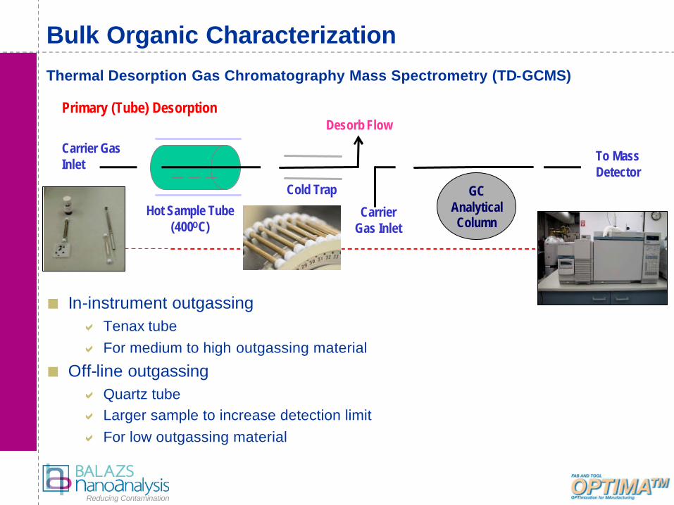
Bulk Organic CharacterizationThermal Desorption Gas Chromatography Mass Spectrometry (TD-GCMS)
_ _ _Carrier Gas Inlet
Hot Sample Tube(400OC)
Cold Trap
Carrier Gas Inlet
GCAnalyticalColumn
To Mass Detector
Primary (Tube) DesorptionDesorb Flow
¢ In-instrument outgassinga Tenax tubea For medium to high outgassing material
¢ Off-line outgassinga Quartz tubea Larger sample to increase detection limita For low outgassing material
Reducing Contamination
Surface Cleanliness of Tool Components Target contaminants depend on the history of the part¢ Starting material
a Gross contaminationa Not a concern as the material will be machined and later cleaneda Bulk contamination is more critical
¢ Machined parta Major contamination is from machine oil, metal cross-contamination,
water and solvent residue, oven, etc.a Machine shops are not semiconductor clean environmentsa Contaminants of concern: Organic > Particle > Metal > Anion
¢ After Precision cleaninga Minor contaminationa Typically from handling, environment, packaging, etc.a Contaminants of concern: Metal > Particle > Organic > Anion
Trend is for machine shops to pre-clean
in-house, outsource Precision
Cleaning and send parts
directly to the customer
a) Precision cleaning is defined as “The removal of undesirable contaminants to a pre-determined measurable standard without introducing new contaminants or changing the surface integrity”
b) Precision cleaning dictates the tool BOM must have a cleanlinessspecification
Reducing Contamination
Surface Contamination Characterization
¢ Applicationa Machined parts – coupons and first articlea New and used parts after Precision Cleaning
¢ Specificationa Effective in removing surface contamination for analysisa Must be damage-free with minimal material lossa Performed on small and large parts (300mm and 450mm)a Part may be returned to the field after testing
¢ Current test methods involving wet chemistrya Imparts minimal damage to the surfacea No restriction on part sizea Effective in removing metals, anions and organic residues since they have a
high solubility in liquid chemistriesa High efficiency in particle removal
• Adjusting the surface zeta potential (e.g. pH) to reduce the adhesion force• Reducing megasonic energy to improve the particle removal performance and to
reduce damage
Reducing Contamination
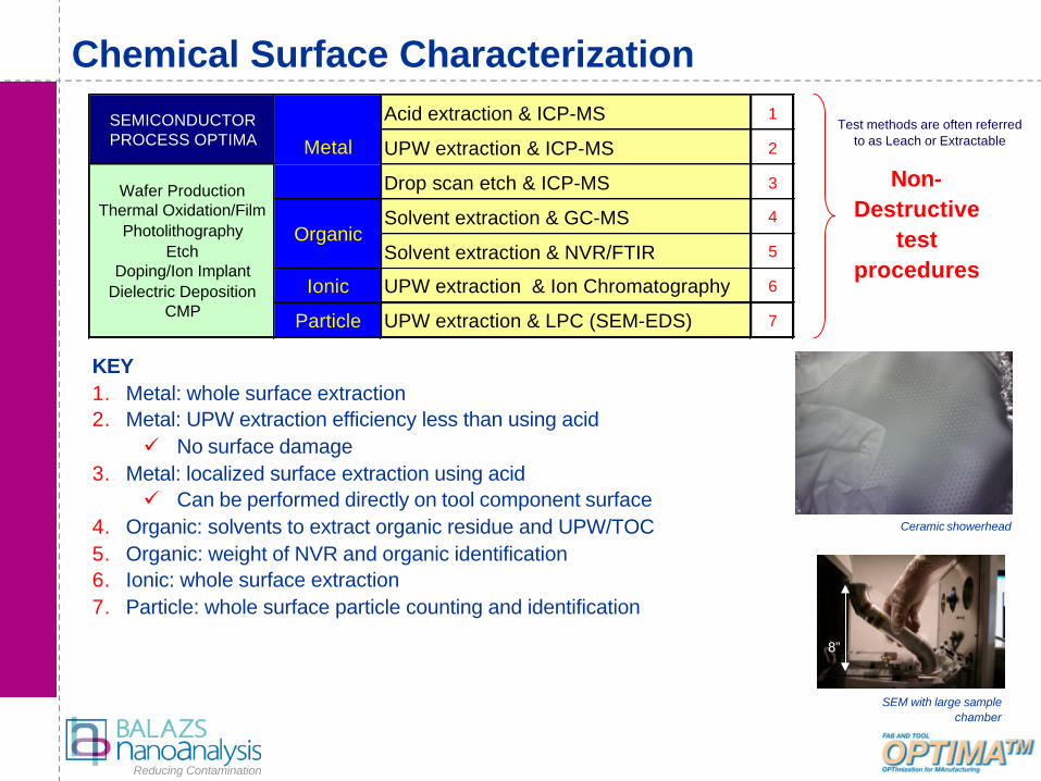
Chemical Surface Characterization
KEY1. Metal: whole surface extraction2. Metal: UPW extraction efficiency less than using acid
ü No surface damage3. Metal: localized surface extraction using acid
ü Can be performed directly on tool component surface4. Organic: solvents to extract organic residue and UPW/TOC5. Organic: weight of NVR and organic identification6. Ionic: whole surface extraction7. Particle: whole surface particle counting and identification
Test methods are often referredto as Leach or Extractable
Acid extraction & ICP-MS 1
UPW extraction & ICP-MS 2
Drop scan etch & ICP-MS 3
Solvent extraction & GC-MS 4
Solvent extraction & NVR/FTIR 5
Ionic UPW extraction & Ion Chromatography 6
Particle UPW extraction & LPC (SEM-EDS) 7
Metal
Organic
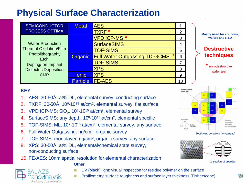
SEMICONDUCTORPROCESS OPTIMA
Wafer ProductionThermal Oxidation/Film
PhotolithographyEtch
Doping/Ion ImplantDielectric Deposition
CMP
Non-Destructive
test procedures
Ceramic showerhead
8”
SEM with large sample chamber

Reducing Contamination
Surface Extraction of Components¢ Provides surface cleanliness verification and quantification of contaminants
a Compare vendorsa Qualify components to a cleanliness specificationa Ensure components and coatings are compatible to a process – temp, exposure time,
acid/alkali, HV, etc.a Lot to lot quality control
¢ General rulea A less aggressive leach results in lower detectable contaminant levela A more aggressive leach results in higher detectable contaminant level
¢ Static leach conditionsa Component is soaked in UPW or chemical solutiona Standard test condition
• Ambient temperature, UPW and short extractiontime of 1h to 1 day
a Semi-Aggressive• Elevated temperature <50C, UPW and short
extraction time of 1-2ha Aggressive
• High temperature, extended extraction time and/or use of chemicals • Chemical for 7 days at ambient temperature• UPW at 85C for 7 days (SEMI F-57)
Ceramic rings

Reducing Contamination
Surface Extraction of Packaging Films
¢ Rule of thumb, the cleanliness level of packaging films should be at least 3-5x lower than the cleanliness specifications of the parts to be packaged
¢ Natural and antistatic PE generally exhibit acceptable levels of ionic cleanliness; generally shown to also be oil and amine-free
¢ Most available films, including natural PE, are not adequate for packaging tool parts requiring very low levels of hydrocarbon contaminants. FEP is acceptable but costs 15x more than PE.
¢ Bagging requirements:a Double bagging for all parts except tool parts (robotic blades, handling systems, chucks) that
are exposed to the wafer must be triple bagged a Bagging material must cover all outer tool surfaces
10
50
40
30
20
Ionic Species
F- Cl- NO3- SO4
- Na+ NH4 + K+ Mg2+
Antistatic PE
Natural PE
Antistatic Nylon
Ca2 +
Lin S and Graves S, Micro, October, 1998
Sur
face
Con
c. (x
1012
mol
/cm
2 )
Reducing Contamination
Metal AES 1
TXRF 2
VPD ICP-MS 3
SurfaceSIMS 4
TOF-SIMS 5
Organic Full Wafer Outgassing TD-GCMS 6
TOF-SIMS 7XPS 8
Ionic XPS 9Particle FE-AES 10
SEMICONDUCTORPROCESS OPTIMA
Wafer ProductionThermal Oxidation/Film
PhotolithographyEtch
Doping/Ion ImplantDielectric Deposition
CMP
Physical Surface Characterization
KEY1. AES: 30-50Å, at% DL, elemental survey, conducting surface2. TXRF: 30-50Å, 109-1015 at/cm2, elemental survey, flat surface 3. VPD ICP-MS: SiO2, 107-1015 at/cm2, elemental survey4. SurfaceSIMS: any depth, 108-1015 at/cm2, elemental specific5. TOF-SIMS: ML, 107-1015 at/cm2, elemental survey, any surface 6. Full Wafer Outgassing: ng/cm2, organic survey7. TOF-SIMS: monolayer, ng/cm2, organic survey, any surface8. XPS: 30-50Å, at% DL, elemental/chemical state survey,
non-conducting surface 10. FE-AES: 10nm spatial resolution for elemental characterization
Other¢ UV (black) light: visual inspection for residue polymer on the surface¢ Profilometry: surface roughness and surface layer thickness (Fisherscope)
Destructive techniques
* non-destructive
wafer test
*
Mostly used for coupons, wafers and R&D
Sectioning ceramic showerhead
**
X-section of opening

Reducing Contamination
Tool Particle Specification
Wafer Front Sidea Wafer Back Sidea Tool Surfaceb
>90 nm
90 nm
65 nm
45 nm
Full pipeline test, 6 wafers, 150 cycles, KLA SP2
Particle SpecificationTechnology Node Analytical Test
Non-Critical Surface≤10/in2 @ 0.3 µm
Critical Surface≤1/in2 @ 0.3 µm0.2 @ 90 nm
(0.0002/cm2 pwp)
Full Contact<1500 @ 90 nm (2.8/cm2 pwp)
Low Contact<500 @ 90 nm
Edge Contact<20 @ 90 nm
a) Tool with closable holes for insertion of sample heads for airborne qualification purposes and FA
b) Particles on tool component surfaces and skin shall be measured using a surface particle detector
Mainframe Surfaces
(particles/in² @ 0.3 µm)
Painted = <10-80Granite = <10-95Anodized = <10-60Aluminum = <15-90Plexiglass = <10-90
Location Area 0.3 um 0.5 um 1 um 5 um 10 umChamber lid 15 0.04 0 0 0 0Chamber lid 16 0.04 0 0 0 0
Location Area 0.3 um 0.5 um 1 um 5 um 10 umChuck/back 10 0.08 0 0 0 0Chuck/front 11 0 0 0 0 0Stage/rear 12 0.21 0.13 0 0 0Stage/front 13 0.08 0 0 0 0
Nest/low surface 6 0.17 0.13 0.08 0 0Nest/high surface 7 0.13 0.08 0 0 0Transfer arm/front 8 0.04 0.04 0.04 0 0Transfer arm/back 9 0.88 0.79 0.58 0 0
Location Area 0.3 um 0.5 um 1 um 5 um 10 umOff LL 1 0.21 0 0 0 0Bridge 2 6.92 3.54 1.6 0.08 0.04
Front LL 3 2.38 1.83 0.96 0.42 0.331
23
45
8
9
10 1
113
12
15
16
¢ The Al/Ti particle originating from an interaction of an etch by-product of the TiN adhesion layer and the process chamber hardware
Ti
Al
Si
Reducing Contamination
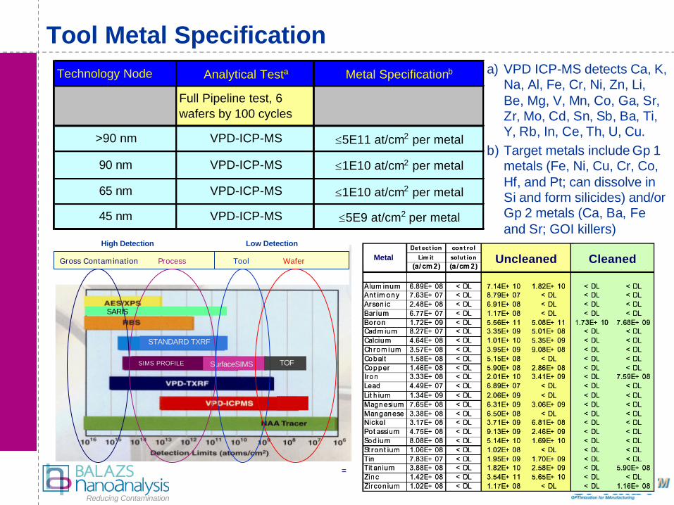
Tool Metal SpecificationTechnology Node Analytical Testa Metal Specificationb
Full Pipeline test, 6 wafers by 100 cycles
>90 nm VPD-ICP-MS ≤5E11 at/cm2 per metal
90 nm VPD-ICP-MS ≤1E10 at/cm2 per metal
65 nm VPD-ICP-MS ≤1E10 at/cm2 per metal
45 nm VPD-ICP-MS ≤5E9 at/cm2 per metal
a) VPD ICP-MS detects Ca, K, Na, Al, Fe, Cr, Ni, Zn, Li, Be, Mg, V, Mn, Co, Ga, Sr, Zr, Mo, Cd, Sn, Sb, Ba, Ti, Y, Rb, In, Ce, Th, U, Cu.
b) Target metals include Gp 1 metals (Fe, Ni, Cu, Cr, Co, Hf, and Pt; can dissolve in Si and form silicides) and/or Gp 2 metals (Ca, Ba, Fe and Sr; GOI killers)
SIMS PROFILE
STANDARD TXRF
=
SurfaceSIMS TOF
High Detection Low Detection
Wafer
SARIS
Gross Contamination Process Tool Uncleaned CleanedMetal
Reducing Contamination
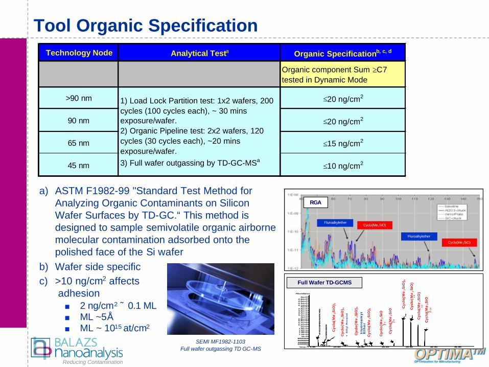
Tool Organic Specification
a) ASTM F1982-99 "Standard Test Method for Analyzing Organic Contaminants on Silicon Wafer Surfaces by TD-GC.“ This method is designed to sample semivolatile organic airborne molecular contamination adsorbed onto the polished face of the Si wafer
b) Wafer side specificc) >10 ng/cm2 affects
adhesion¢ 2 ng/cm2 ˜ 0.1 ML¢ ML ~5Å¢ ML ~ 1015 at/cm2
Technology Node Analytical Testa Organic Specificationb, c, d
Organic component Sum ≥C7tested in Dynamic Mode
>90 nm ≤20 ng/cm2
90 nm ≤20 ng/cm2
65 nm ≤15 ng/cm2
45 nm ≤10 ng/cm2
1) Load Lock Partition test: 1x2 wafers, 200 cycles (100 cycles each), ~ 30 mins exposure/wafer.2) Organic Pipeline test: 2x2 wafers, 120 cycles (30 cycles each), ~20 mins exposure/wafer.3) Full wafer outgassing by TD-GC-MSa
SEMI MF1982-1103Full wafer outgassing TD GC-MS
Figure 1
Sample ID: CHUCK- Al2O3, 1/22/07 (19:00 HOURS AT 1.2 x 10- 7 TORR)
5.00 10.00 15.00 20.00 25.00 30.00 35.000
2000000400000060000008000000
1e+071.2e+071.4e+071.6e+071.8e+07
2e+072.2e+072.4e+072.6e+072.8e+07
3e+073.2e+073.4e+073.6e+073.8e+07
4e+074.2e+074.4e+074.6e+074.8e+07
5e+07
Time-->
AbundanceIon 33.00 (33.00 to 700.00): 70052605.D
d8-TOLU
ENE (INTE
RNAL ST
ANDARD)
C8-H
YDROCARBONS
CYCLO
(Me 2S
iO) 3
CYCLO
(Me 2S
iO) 4
+ ETH
YL H
EXANOL
CYCLO
(Me 2S
iO) 5
FLUOROALKYL ETHER (m/z:69,119,169,285,335)
CYCLO
(Me
2SiO) 6
CYCLO
(Me 2SiO) 7
CYCLO
(Me 2S
iO) 8
CYCLO
(Me
2SiO) 9
CYCLO
(Me 2S
iO) 10
CYCLO
(Me 2S
iO) 11
POSSIBLE
CYCLO
(Me
2SiO) 12
Cyclo(Me 2SiO)
Cyclo(Me 2SiO)Fluroalkylether
Fluroalkylether
Flu
oro
alk
yl
Eth
er
RGA
Cycl
o(M
e2S
iO) 3
Cycl
o(M
e2S
iO) 5
Cycl
o(M
e2S
iO) 6
Cycl
o(M
e2S
iO) 7
Cycl
o(M
e2S
iO) 8
Cycl
o(M
e2S
iO)
10
Cycl
o(M
e2S
iO) 1
2
Cycl
o(M
e2S
iO) 4
+ E
thyl
Hexan
ol
Cycl
o(M
e2S
iO) 9
Cycl
o(M
e2S
iO)
11
Full Wafer TD-GCMS

Reducing Contamination
Tool Escalation Case Study
TOOL ESCALATIONTOOL
OBSERVATIONSFAILURE ANALYSIS ROOT CAUSE REMEDY
High SMC carbon level exceeding tool acceptance level of 2 at% by XPS
7 carbon at% on witness wafer
Full Wafer TD-GCMS to identify AMC-MC species. FTIR and TOF-SIMS to identify lubricant compound.
Excess lubricant in toolRemove excess lubricant
High Cl TXRF level exceeding 5E10 at/cm2 spec for acceptance
5E13 Cl at/cm2 on witness wafer
Determine inorganic Cl using IC or organic Cl using GCMS. O-Cl confirmed followed by species identification using Full Wafer TD-GCMS in dynamic testing mode.
Foam isolation padsTD-GCMS verification of alternative materials
High Pb level by VPD ICP-MS exceeding 5E10 at/cm2 tool SPC
5E11 Pb at/cm2 on witness wafer
VPD ICP-MS monitoring was critical as Pb is not detected by TXRF using W source. Isolation experiments identified root source.
City water source used during manufacturing of PVDF tubing
Hot DIW flush of tubing
High replacement rate of beam aperture on ion implanter
Reduced beam current
SEM-EDX identifies organo-Si as contaminant on aperture. TD-GCMS identifies organic species.
Outgassing of Gelpak aperture packaging
TD-GCMS verification of alternative packaging
Metal spec is 5E10 at/cm2 by TXRF
1Residual HCl from insufficient
rinsing??
2
INORGANIC ORGANIC
SARIS/SEM-EDX First “look” tool
LOW CONC.
VPD ICP-MSTXRF, VPD TXRF
UPW – ICUPW-ICP-MSdAcid-ICP-MS
TOF-SIMSQuad-SIMS
LOW CONC.
TOF-SIMSFW TD-GCMS
TD GC-MS
4Static wafer show no Cl by TXRFDynamic wafer testing show Cl
3
Pad compresses and outgasses at edge
6Blue pad outgassBlk pad not outgas
7
Cl
Flame retardant5
This is a difficult problem to solve because no one did anything wrong. In fact, everyone involved did what they thought was the right thing to expedite the PM and keep on schedule.
8
Reducing Contamination
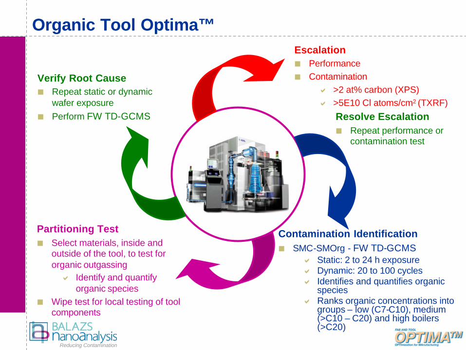
Organic Tool Optima™Escalation¢ Performance¢ Contamination
a >2 at% carbon (XPS)a >5E10 Cl atoms/cm2 (TXRF)
Partitioning Test¢ Select materials, inside and
outside of the tool, to test for organic outgassing
a Identify and quantify organic species
¢ Wipe test for local testing of tool components
Contamination Identification¢ SMC-SMOrg - FW TD-GCMS
a Static: 2 to 24 h exposurea Dynamic: 20 to 100 cyclesa Identifies and quantifies organic
speciesa Ranks organic concentrations into
groups – low (C7-C10), medium (>C10 – C20) and high boilers (>C20)
Resolve Escalation¢ Repeat performance or
contamination test
Verify Root Cause¢ Repeat static or dynamic
wafer exposure¢ Perform FW TD-GCMS
Reducing Contamination
Conclusion¢ Tool contamination is a major cause of many fab escalations¢ High yield processing requires clean tools and clean manufacturing
procedures. This dictates there must be cleanliness specification for in-tools, precision cleaning, packaging and on the process floor (Ex: housekeeping cleanliness specifications)
¢ Unfortunately, cleanliness specifications are often lacking and this impounds the difficulty to resolve contamination escalations, both in the tool and on the process floor
¢ Bulk and surface contamination of starting material and tool components are equally important
¢ Target contaminants differ for a part and depends on its life cycle – from raw material, coupon, first article, new part, used part, etc.
¢ Non-destructive chemical characterization is possible on production tool parts¢ Destructive physical characterization on production tool parts is an option if you
are willing to sacrifice the part¢ Cleanliness verification of tool BOM is instrumental to optimizing process
yields. Advanced technology node processes require stringent cleanliness specifications, lower analytical detection limits and clean handling technique