to the graduate council - university of tennessee - power electronics lab...
TRANSCRIPT

To the Graduate Council:
I am submitting herewith a thesis written by Shibani Mishra entitled “Fault current
limiting and protection circuit for power electronics used in a Modular Converter.” I have
examined the final electronic copy of this thesis for form and content and recommend
that it be accepted in partial fulfillment of the requirements for the degree of Master of
Science, with a major in Electrical Engineering.
_______________________
DR. LEON M TOLBERT
MAJOR PROFESSOR
We have read this thesis and recommend its acceptance:
_______________________
DR. FANGXING LI
_______________________
DR. JACK S LAWLER
Accepted for the council:
_______________________
Carolyn R. Hodges, Vice Provost and
Dean of the Graduate School
(Original signatures are on the file with official student records.)

Fault Current Limiting and Protection Circuit for Power Electronics
used in a Modular Converter
Thesis
Submitted for
Master of Science Degree
The University of Tennessee, Knoxville
Shibani Mishra
December 2008

ii
Acknowledgment
I would like to thank everyone who helped me make this thesis a success. First
and foremost, I would like to thank my advisor Dr. Leon M Tolbert for guiding me
through every step with utmost patience. I would like to thank him immensely for all
that I have learnt through my thesis. I admire his vast knowledge, methodical and
diligent approach to research. I consider myself extremely lucky to have him as my
advisor.
I would like to thank my other committee members, Dr. Fangxing Li and Dr.
Jack Lawler for being a constant support and source of guidance through my thesis
process. I would like to thank Mr. Madhu Chinthavali for always being approachable to
any questions or doubts I had regarding my work. He has always encouraged me and
answered my queries. His constant guidance helped me in working towards my thesis
completion.
I would like to thank my family, my parents, my sister, and my brother for
always being there for me and believing in me. I thank them for their constant support
through my Master’s program and through my thesis process.
I am extremely grateful to my friends Simi, Manpreet, Neha, Vinay, and
Ashutosh for being there for me until I finished my thesis work. They have always
offered to help me with my work. They have been a constant source of support, staying
up late nights and encouraging me. They made the entire process much easier on me.
Finally I would like to thank all my lab mates and people working at the
Innovative Technology Center who were very co-operative and accommodating during
my entire Masters program.

iii
Abstract
The thesis objective is to safeguard power electronics used in modular converter
applications. A new fault current limiting and protection circuit is proposed. The system
level fault mitigation assemblies take a long time to remove a fault and within this time
the IGBTs used in the Flexible AC Transmission System (FACTS) application will
undergo high thermal and mechanical stress. Exposure to such conditions over a
prolonged period of time will reduce the device lifetime, which is one of the major
reasons why power electronics are not very popular in utility applications. Modular
converter approach will reduce the device ratings required to mitigate the fault at power
electronics level. The fault current limiting and protection circuit is tested using PSPICE
simulation tool. The test set up is simple comprising of two IGBTs, one which acts as
device under test (DUT) and another which acts as switch regulating fault seen by DUT.
The test voltage is 480 Volt and R-L is varied over a range of L – 20nanoHenry,
2microHenry, and 10microHenry and R – 20Ohm, 50Ohm, and 100Ohm. The fault
current limiting (FCL) and protection circuit worked accurately in each of the cases
described above, thereby safely turning OFF the device within the short circuit withstand
capacity (10microseconds) of IGBTs. The FCL and protection circuit can mitigate both
Hard Switched Fault and Fault Under Load seen by the IGBT during short circuit
condition. The circuit developed is different from the conventional protection gate drives
available in the market and there is the possibility of customizing it further for modular
blocks.

iv
Table of Contents
CHAPTER 1 INTRODUCTION.............................................................................................................1
1.1 Facts & Distributed Generation for Future Application................................................1
1.2 Shift from Multilevel to Modular Converter.................................................................3
1.3 Existing Fault Protection Technology for Power System………………………….….4
1.4 Faults in IGBT………………………………………………………………………...8
1.4.1 Fault under Load (FUL)…………………………………………………….…..8
1.4.2 Hard Switched Fault (HSF)…………………………...…………………….…..9
1.4.3 Effects of Short Circuit on IGBT…………….……………………………….…10
1.4.3.1 Exceeding the temperature limit…….……………………..……………10
1.4.3.2 Latching………………………………….……….……………………...11
1.4.3.3 Exceeding Voltage Rating……………….………………………………..11
1.4.3.4 Turn-on failure mode…………………….………….…………………….11
1.5 Circuit Breakers Vs Power Electronics Fault Limiting…….……………………..…12
1.6 System level fault simulation model in PSCAD/EMTDC ….…………………...….14
1.7 Summary………..…………………………………………….……………………...18
List of Chapters………………………………………………………………………...19 CHAPTER 2 REVIEW OF LITERATURE…...................................................................................20
2.1 Detection of fault current………………………………….......................................21
2.1.1 Detection through resistance...........................................................................21
2.1.2 Current Transformer…………………………………………………………21

v
2.1.3 De-saturation Detection (Collector Voltage)..……………………………….21
2.1.4 Gate Voltage Detection………………………………………........................22
2.2 Review of Fault Protection Circuit............................................................................22
2.3 Fault Current Limiting Circuit (FCLC) [1] ………………………………………...23
2.4 Device Level Fault Protection in STATCOM……………………………………...26
2.5 Protection Technique Used in Modular Converter………………………………….27
2.6 Summary…………………………………………………………………………….30
CHAPTER 3 METHODOLOGY......................................................................................................... 31
3.1 PSPICE simulation model…….................................................................................. 31
3.1.1 Simulation model without FCLC protection……..………………………..…...34
3.1.2 Simulation model with FCLC protection…………………………………..…..35
3.1.2.1 IXDD414 – Gate drive circuit (G1)……………………………………36
3.1.2.2 HCPL – 316J – Optocoupler (O1)……………………………………..37
3.1.2.3 LM317K – Voltage Regulator (U6)…………………………………....38
3.1.2.4 LM311 – Comparator (U1 & U2)………………………………….......39
3.1.2.5 HCPL-4506 – Optocoupler (O2)……………………………………....42
3.2 Uniqueness of proposed FCL and protection circuit………………………………...42
3.3 Summary……………………………………………………………………………..43
CHAPTER 4 RESULTS.........................................................................................................................44
4.1 IGBT characteristics under fault, without protection circuit………………………...44
4.1.1 Fault Under Load condition……………………………………………………..45
vi
4.1.2 Hard Switched Fault condition…………………………………………………..47
4.2 IGBT characteristics under fault, with protection circuit……………………………49
4.2.1 Hard switched fault with protection circuit……………………………………...50
4.2.2 Fault under load condition with protection circuit…………………………........52
4.2 Observations made under varying R-L load conditions……………………………..55
4.3 Summary……………………………………………………………………………..56
CHAPTER 5 CONCLUSION AND FUTURE WORK.......................................................................57
5.1 Conclusions .................................................................................................................57
5.2 Future Work.................................................................................................................59
5.3 Summary......................................................................................................................60
REFERENCES.................................................................................................................61
Vita ...................................................................................................................................64

vii
List of Figures
Figure 1.1 Fault under load test circuit …………………………………………………...8
Figure 1.2 Hard switched fault test circuit ………………………………………………10
Figure 1.3 Equivalent circuit of IGBT …………………………………………………..11
Figure 1.4 PSCAD/EMTDC system level fault simulation circuit………………………14
Figure 1.5 Fault Resistance equivalent circuit………………………………….………..15
(a) Three Phase to Ground
(b) Phase to Ground
(c) Phase to Phase,
(d) Phase to Phase to Ground
Figure 1.6………………………………………………………………………………...17
a) IGBT number 6 voltage characteristic, and
b) IGBT number 6 current characteristic
Figure 2.1 Simplified circuit used to simulate the IGBT characteristics with a
fault current limiting gate drive …………………………………………………………25
Figure 3.1 Simulation model without FCLC protection circuit …………………………34
Figure 3.2 Simulation model with fault protection circuit……………………………….35
Figure 3.3 IXDD414 gate drive………………………………………………………….36
Figure 3.4 HCPL-316J Optocoupler………………………………………………..........37
Figure 3.5 Voltage regulator model Lm317K……………………………………………38
Figure 3.6 Comparator U1 for Under-Voltage lockout.…………………………………39

viii
Figure 3.7………………………………………………………………………………...41
(a) gate over-voltage limiting circuit
(b) Comparator circuit for gate over-voltage detection
Figure 3.8 Simulation for testing HCPL-4506 and IXDD414 interconnection..………...42
Figure 4.1 Fault under load condition without protection..……………………………...46
Vce, Ic and Vge waveform for
a) IGBT IXGH40N60
b) IGBT IXGH28N120BD
Figure 4.2 Hard Switched fault without protection Vce, Ic and Vge waveform for……..48
a) IGBT IXGH40N60
b) IGBT IXGH28N120BD
Figure 4.3 Hard switched fault with protection, Vce, Ic and Vge characteristics……….51
a) DUT is IXGH40N60, and b) DUT is IXGH28N120BD
Figure 4.4 Fault under load with protection, Vce, Ic and Vge characteristics…………...53
a) DUT is IXGH40N60
b) DUT is IXGH28N120BD
Figure 4.5 Gate Voltage Vge characteristic……………………………………………...54
a) without over-voltage protection
b) with over-voltage protection

ix
List of Tables
Table 1.1 Comparison of fault mitigation time…………………………………………..12
Table 1.2 Current and Voltage percentage increase during fault………………………...16
Table 4.1 Tdesat and Peak fault current for DUT during hard switched fault, varying load
R-L……………………………………………………………………………………….55
Table 4.2 Tdesat and Peak fault current for DUT during fault under load, varying load R-
L………………………………………………………………………………………….56

1
CHAPTER 1: INTRODUCTION
Isolated Gate Bipolar Transistors (IGBT) are widely used in converters nowadays
due to their low duty cycle, high voltage application, as well as ability to operate at low
frequencies and high junction temperatures. However, despite these advantages, there is a
tradeoff between the performance and fault-handling capacity of an IGBT, i.e. there is a
need for improved switching performance along with ruggedness. The lifetime of an
IGBT can be increased by having an inbuilt protection circuit which in turn improves the
ruggedness or robustness of the device. This thesis analyzes various fault current limiting
circuits available in the market and proposes a new fault current limiting circuit for
improving the performance of power electronics used in modular converters.
1.1 Facts and Distributed Generation For Future Application
Much of the energy generated today is produced by large-scale, centralized power
plants using fossil fuels (coal, oil and gas), hydropower or nuclear power, with energy
being transmitted and distributed over long distances to consumers. In this paradigm,
power flows only in one direction: from the central power station to the network and to
the consumers. There are a number of drawbacks to such a system, such as the high level
of dependence on imported fuels, the environmental impact of greenhouse gases and
other pollutants, transmission losses and the necessity for continuous upgrading and
replacement of transmission and distribution facilities.
In contrast, in a power system composed of distributed energy resources, much
smaller amounts of energy are produced by numerous small, modular energy conversion
units, which are often located close to the point of end use. These units can be stand-
alone or integrated into the electricity grid. Flexible AC Transmission Systems (FACTS)

2
will provide ways to control the routing of electricity and also provide flexible distributed
generation (DG) interfaces to the network. Hence, this creates a need for developing new
FACTS technology, which will improve the market for DG sources and make way for its
widespread use.
FACTS is defined by the IEEE as "a power electronic based system and other
static equipment that provide control of one or more AC transmission system parameters
to enhance controllability and increase power transfer capability." The various types of
FACTS controllers are mentioned below-
• Series Controller – It injects voltage in series with the transmission lines, example
Static Synchronous Series Compensator (SSSC)
• Shunt Controller – It is shunt connected in order to exchange capacitive or
inductive current with the system at a coupling point, example Static Synchronous
Compensator (STATCOM)
• Combination of Series-Shunt Controller – It is a combination of series and shunt
controller, example Unified Power Flow Controller (UPFC) consists of a
STATCOM and SSSC which are coupled via a common dc link to allow bi-
directional flow of real power between the series output terminals of SSSC and
the shunt output terminals of the STATCOM
• Combination of Series-Series Controller – It is a series connected controller of
active and reactive power consisting in each phase of inductive and capacitive
branches subjected to separately phase-shifted voltages, example Inter-phase
Power Controller (IPFC).

3
In this thesis, a STATCOM is considered for comparative study. STATCOM
technology is more popular in utility system due to its ease in interconnection and
improved topologies. The modular converter topology is developed in order to provide a
flexible alternative to the existing STATCOM multilevel topology.
1.2 Shift from Multilevel to Modular Converter
The different multilevel topologies available are-
• Diode-clamped multilevel converter
• Flying-capacitor multilevel converter
• Cascaded multilevel converter
Cascaded multilevel converter provides modularity to the existing converter system
and has an edge over rest of the multilevel topologies due to –
1. easy expansion
2. easy to achieve higher power rating
3. easy to add redundancy
4. least number of components
However, in spite of advantages mentioned above, the conventional centralized
controller architecture employed in cascaded multilevel converter has created the need
for a modular approach. For each modular converter there is a local controller, which
provides intelligence to the converter. The local controller can reconfigure itself for
different power processing such as AC-DC, DC-DC and DC-AC. The following features
tend to give an advantage to modular converter-
• Flexibility for expansion
• Less connection between central and local controllers

4
• True optical fiber connections between central and local controllers
• Easy reconfiguration capability
• Analog sensing signals conditioning
• Simple communication protocol between central and local
controllers
• Easy to locate faults due to local controllers
The building block of a modular converter can either be Power electronics
building block (PEBB) or H-bridge building block (HBBB). This thesis does not deal
with the design of modular blocks. It only addresses to improving the lifetime of IGBTs
to be used in modular converter by safeguarding it against extreme conditions caused due
to fault externally (system level) or internally (device level). The next section looks into
the available technologies for protecting utility systems against faults and their
shortcomings, thereby, making way for developing protection circuits for IGBTs used in
utility applications.
1.3 Existing Fault Protection Technology for Power System
In a power system, faults can be characterized into symmetric and asymmetric
based on its effect on the three phases of the system. As the name suggests, symmetric
faults have the same effect on all three phases, however asymmetric fault does not effect
all three phases equally. Asymmetric faults are more common in utilities. Shunt/Short
circuit faults are asymmetric and result in a high current flowing through the system.
These high currents can destroy the power electronics involved in the converter. Hence
timely and accurate protection circuits along with fault removal techniques have to be

5
implemented to overcome shunt fault conditions. The four types of shunt faults are as
follows –
1. Three phase short circuit
2. Line to Line
3. Line to Ground
4. Two Line to Ground
Short circuit current produced in the system causes mechanical and thermal stress.
The magnitude of the short circuit current is dependent on the location of the fault in the
system. Also the total current flowing to the fault depends on the type of fault and the
phase in which the current is measured.
There are some other system configurations that are not short circuit but still
considered as faults. These are grouped together as longitudinal fault as opposed to lateral
faults or short circuit faults. These faults are –
1. One line open
2. Two lines open
3. Three lines open
The first two faults cause unbalanced current flow in a 3-phase system and will
require a protective system only if the unbalance poses a threat to the system. The third
fault however does not require any special protection circuit. As the longitudinal faults do
not pose a serious threat to the system, only shunt fault is taken into consideration while
devising a protection topology.
Most of the utility systems heavily rely on circuit breakers and relays for protection
against fault situations. Circuit breakers serve to open the faulted circuit and thereby to

6
sever it from the sound part of the power system. They are required to interrupt
abnormally large currents. Protective relays serve to detect the presence of faults, to
determine their locations, and to initiate the opening of the proper circuit breakers. To
isolate a fault with the least interruption of service to customers and with the least shock
to the synchronous machines, only the faulted circuit and no other should be
disconnected. This requires the use of relays, which will select correctly the circuit
breakers that should be opened. In addition, both the relays and the circuit breakers
should act as rapidly as possible consistent with selectivity.
The majority of faults in overhead transmission lines are due to lightning which do
not cause any permanent damage. In these cases rapid mitigation and re-closure of the
protection device will ensure restoring of supply to consumer and safeguard from any
faults which may occur later. Based on the speeds of circuit breakers and relays, it is
divided into following categories –
• Slow-speed circuit breaker and relays
• High-speed circuit breaker and relays
• High-speed re-closing circuit breaker and relays
The clearing time is the sum of the relay time and breaker interrupting time. The
relay time is the elapsed time from the instant when a fault occurs until the instant when
the relay contacts close the trip circuit of the circuit breaker. The breaker interrupting
time is based on the instant the relay contacts close the trip circuit until the instant when
the current is interrupted. It is the sum of the breaker opening time and the arcing time.
Re-closing time is the elapsed time from the instant of energizing the trip circuit, the
breaker being in the closed position, until the instant when the breaker arcing contacts

7
touch on the re-closing stroke; it includes breaker opening time and time during which
the breaker is open. All these times, if short, are customarily expressed in cycles on the
basis of the usual power-system frequency of 60 cycles per second.
Slow-speed circuit breakers and relays have a clearing time of 21 to 150 cycles.
With such slow clearing, the power limits were but little higher than the limits with
sustained faults. Many slow-speed breakers and relays are still in use where rapid
clearing is not necessary.
High-speed circuit breakers have a clearing time of 5-8 cycles, and along with
relay operation time of 1- 3 cycles, the entire clearing time can be reduced to 6-8 cycles
for 5 cycle circuit breaker or 9-11 cycles for 8-cycle circuit breaker.
Until very recently, few alternatives to electromechanical and magnetic circuit
breakers existed. Designers were forced to live with such undesirable characteristics as
arcing and switch bounce (with corresponding noise and wear), while accommodating
large unwieldy packages in their high power systems. Solid state technology applied to
this traditional device has resulted in circuit breakers free from arcing and switch bounce,
that offer correspondingly higher reliability and longer lifetimes as well as faster
switching times. A typical solid-state circuit breaker will switch in a matter of
microseconds, as opposed to milliseconds or even seconds for a mechanical version. New
solid-state products currently on the market utilize the many benefits associated with
power MOSFETs to deliver a product far superior to earlier silicon versions. Power
MOSFETs offer low on resistances (as compared to bipolar transistors), low voltage
drops, low EMI, faster switching times and good thermal stability of key parameters.

8
However, major drawbacks of solid-state circuit breakers are material costs and ON-state
losses. There is ongoing work in overcoming these disadvantages.
Solid state breakers have a correction time of 100μs in comparison to 100ms in
electromechanical fault correction systems hence this could be a preferred choice for
protection of devices in combination with self protection in gate drives.
1.4 Faults in IGBT
To reduce complexity of operation, this thesis focuses on device level faults that
disrupt the normal operation of an IGBT resulting in faulty converter operation. At device
level, faults can be characterized into over-current, short circuit, open circuit faults etc.
Short circuit faults are most critical to the device. An IGBT has an inherent short circuit
withstand time of 10μs and the aim of the protection circuits is to clear the fault within
this time. The two main short circuit fault types are –
1. Fault under Load
2. Hard Switched Fault
1.4.1 Fault under Load (FUL)
Figure 1.1 Fault under load test circuit

9
Short circuit of a device during its on state results in fault under load condition.
FUL condition can be further explained by referring to the test circuit in Figure 1.1,
where short circuit occurs when the IGBT referred to as Switch turns on when the DUT is
on. This fault results in a rise in the collector emitter voltage, which in turn increases the
gate emitter voltage (Vge) because of the collector gate current driven through the Miller
capacitance (Cgc). This high Icg current pulls the DUT into the active region from near
saturation state. When the voltage transient dies down, the collector current declines as
Vge settles to its low on-state value. In FUL condition, gate resistance (Rg) plays a
significant role. Low values of gate resistance limit the value of Vge and increases the
short circuit withstand time. However, a low value of Rg has adverse effects on over
voltage, i.e., dv/dt during turn off. Therefore the value of Rg should be decided keeping
this trade off in mind [7].
1.4.2 Hard Switched Fault (HSF)
In this case, as seen in Figure 1.2, short circuit occurs when DUT is turned on
from off state resulting in the entire system voltage Vdc being supported across the
device. The magnitude of fault current and di/dt is directly proportional to the charging
rate of input capacitance and gate drive voltage (Vg). The fault current can be removed
by turning off the gate, thereby causing a rapid fall in fault current. This rapid fall in fault
current combined with the DC loop inductance directly affects the over voltage caused
due to rise in Vce. Adjusting the gate resistance, Rg, can control the fall rate of fault
current as well as the rise in Vce. However, a trade off has to be kept in mind before
settling on a particular value of Rg, i.e. effect of large Rg on short circuit withstand time,
gate noise immunity, dv/dt capability etc.

10
Figure 1.2 Hard switched fault test circuit
In HSF, the dv/dt is small in comparison to FUL, hence Miller capacitance does
not have any significant influence. Moreover, the fault current in HSF is less than FUL,
which is why many manufacturers use HSF test to specify their short circuit capabilities,
as it is less stressful [7].
1.4.3 Effects of Short Circuit on IGBT
The most common cause of device failure during short circuit is power dissipation
resulting in high temperatures beyond the thermal capacity of device. The short circuit
modes are described in the following sections–
1.4.3.1 Exceeding the temperature limit
High power dissipation due to short circuit causes a rise in temperature of the die.
Due to the high thermal time constant, the rate dT/dt (rise in temperature) is very high
and hence if short circuit is not taken care of quickly, it will lead to the destruction of the
device. After the doped silicon becomes intrinsic, i.e. at around 250°C, further rise in
junction temperature causes an exponential increase in carrier concentration resulting in
thermal runaway, and beyond 900°C silicon becomes fatally damaged.

11
Figure 1.3 Equivalent circuit of IGBT
1.4.3.2 Latching
Latching condition occurs when excess current starts to flow through parasitic
resistor rb/ (shown in Figure 1.3) causing a voltage across the resistor. Once the IGBT is
in latched condition, control of the gate is not possible. Hence, the device can withstand
long short circuit time but still fail during turn off due to dynamic latching.
1.4.3.3 Exceeding Voltage Rating
The fall rate of current induces a voltage equivalent to L di/dt, where L is the DC
loop stray inductance. A high value of this voltage will cause the device to avalanche
resulting in excessive power surge or latching. This mode of failure can be avoided or
limited by either reducing the fault current or DC loop inductance. The fall in fault
current can be reduced by suitably choosing turn-off series gate resistor Rg(off) of higher
value.
1.4.3.4 Turn-on failure mode [6]
A new failure mode has been detected characterized by a sudden decrease in short
circuit handling capability when both the applied voltage and the gate voltage exceed a
certain value.

12
Table 1.1 Comparison of fault mitigation time
Protection System Time in seconds Cycles as in 60 cycles in 1 sec
Level
Slow speed Circuit Breaker and relay
0.35 -2.5 s 21-150 System
High Speed Circuit Breaker and relay
100 – 183 ms 6-11 System
Solid State Circuit Breaker
100 μs 0.006 System
Gate Drive with inherent protection
<10 μs 0.0006 Device
1.5 Circuit Breakers vs. Power Electronics Fault Limiting
As seen in the Table 1.1 above, most of the fault clearing mechanisms fail to limit the
fault within the short circuit withstand time of devices (10μs). The fault current seen by
the device over a prolonged period of time will lead to device destruction and/or
reduction in the lifetime of power electronics involved in utility system. In case there is
short circuit in the converter legs, then external protection circuit will not be able to
mitigate such faults and this further reduces the lifetime of the device. The cost of having
an additional protection circuit is overshadowed by its advantages. Some of the
advantages of fault current limiting power electronics are mentioned as follows-
1. Fast response so that the line does not see the first peak of the fault current.
Response time in μs will prevent destruction of the device thereby increasing
converter lifetime. The fault current will be reduced with the help of gate voltage
control circuitry.
2. Circuit breakers and conductors do not have to be de-rated since the peak fault
current is limited.

13
3. Device is environmental friendly as no inflammable liquids like oil or SF6 are
required.
4. Longer lifetime for power electronics converter (around 30 – 50 years).
5. Longer lifetime for transformers since high fault currents will not flow.
6. Operation within rated junction temperature.
7. More reliability and robustness.
8. Steady state operation independent of protection circuit.
Normally in cases where circuit breakers are unable to remove the fault, the power
electronics involved in the converters should have fault current limiting capability.
Instead of circuit breakers, it would be convenient to use a switch or relay that could be
reset so that once the fault is cleared the system can be brought to normal operation
without the need to replace fuse or similar mechanical operation. The system level fault
corresponds to the faults in the utility system. A combination of fast acting solid state
breaker which has a mitigation time of 100 μs and a gate drive having inherent fault
current limiting protection will ensure longer lifetime and safeguard the IGBTs from
thermal and mechanical stress. For example – in case the IGBT has a switching
frequency of 20 kHz then the fault current limiting circuit can reduce the fault current for
at least 20 μs without switching off the device then within the next 30 μs the device will
turn off based on switching frequency. The next time the device is on i.e., after 100 μs,
the solid-state circuit breaker will ensure the module is isolated in case the fault system or
device level, still persists.
The next section shows the effect of shunt faults on IGBTs used in STATCOM using
PSCAD v4.2. PSCAD/EMTDC tool mainly deals with analyzing HVDC systems. In this

14
thesis it has been used to create a background to illustrate the effect of short circuit faults
in system on the IGBT devices used in FACTS. This paves the way for the need of fault
current limiting circuits for power electronics used in the utility systems.
1.6 System level fault simulation model in PSCAD/EMTDC
The simulation is an example in the PSCAD/EMTDC kit. The simulation device
has been modified for power electronics required for this thesis i.e., IGBT. The snubber
circuit has been removed as it could lower the fault current, and voltage level seen across
the IGBT. The AC system rating is – Voltage 115kV, Frequency 60 Hz, Short Circuit –
500 MVA, and Load rating is – 88 MVA with power factor 0.906. The Y/∆ step down
transformer reduces the 3 phase line voltage from 115kV to 28kV, and has a power rating
of 100 MVA.
Figure 1.4 PSCAD/EMTDC system level fault simulation circuit
15
(a) (b)
(c) (d)
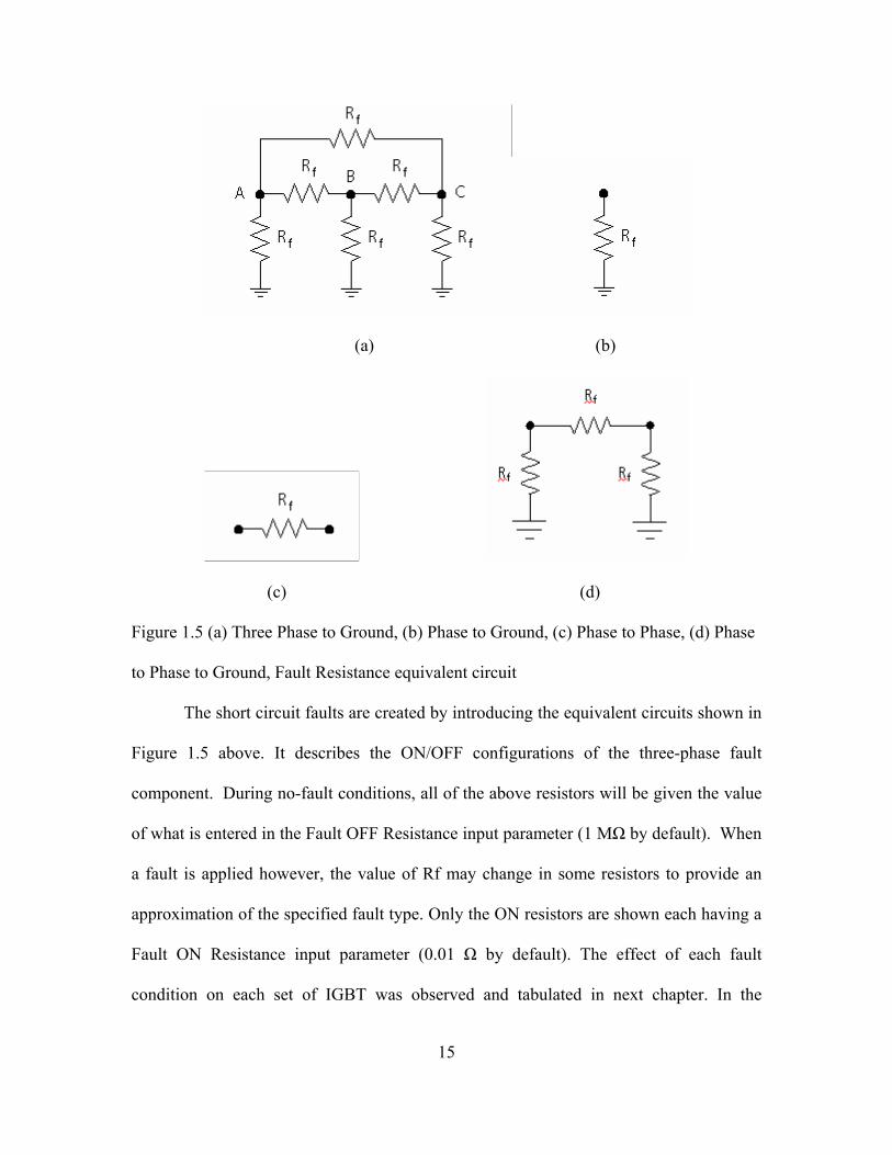
Figure 1.5 (a) Three Phase to Ground, (b) Phase to Ground, (c) Phase to Phase, (d) Phase
to Phase to Ground, Fault Resistance equivalent circuit
The short circuit faults are created by introducing the equivalent circuits shown in
Figure 1.5 above. It describes the ON/OFF configurations of the three-phase fault
component. During no-fault conditions, all of the above resistors will be given the value
of what is entered in the Fault OFF Resistance input parameter (1 MΩ by default). When
a fault is applied however, the value of Rf may change in some resistors to provide an
approximation of the specified fault type. Only the ON resistors are shown each having a
Fault ON Resistance input parameter (0.01 Ω by default). The effect of each fault
condition on each set of IGBT was observed and tabulated in next chapter. In the

16
simulation circuit the fault impedance is 75 Ω having X/R ratio of 1. The fault starts at
1.5 seconds and lasts for 0.75 seconds.
Phase A to ground fault was introduced in the system that resulted in waveforms
shown in Figure 1.6 a), and b). The voltage increased by 20% of normal value, whereas
current during the fault was almost 1.67 times that of current value at normal operating
condition.
Table 1.2 demonstrates the percentage increase in current and voltage during
different fault conditions. The highest percentage increase was seen in 3-phase to ground
fault followed by 2-phase to ground, then 2-phase and finally 1-phase to ground. The
fault being A->G the effect of fault on IGBT 6 was least during 1-phase to ground
because the IGBT is connected to phase B. Seeing the impact of system fault on an IGBT
module comprising of several IGBTs in series/parallel (dependent on module rating), it is
preferable to use a inherent protection scheme to safeguard IGBTs from high currents
over a prolonged period of time (several years). The thermal and mechanical stress will
build up over the years finally leading to shortening of IGBT lifetime.
Table 1.2 Current and Voltage percentage increase during fault
Serial No Fault Type Maximum Fault
Current (kA)
Percentage Increase (%)
in current
Maximum Fault
Voltage (kV)
Percentage Increase (%)
in voltage
1 ABC G 11.1 267 70 40
2 AB G 9.1 200 66 30
3 A G 5 67 60 20
4 AB 8 167 68 36

17
(a)
(b)
Figure 1.6 a) IGBT number 6 voltage characteristic, and b) IGBT number 6 current
characteristic

18
Here an example of STATCOM was taken where usually GTOs are used instead
of IGBTs because of higher ratings. However for modular converter applications, IGBTs
are the ideal choice for power electronics because of reasons already mentioned in this
chapter.
1.7 Summary
The purpose of this thesis is to test a circuit which is capable of limiting fault
current seen by the power electronics used in a modular converter. The power electronics
device used for this thesis is an IGBT which is the preferred choice for high voltage
applications. The aim of the thesis is to:
i. test the current limiting capability of protection circuit under HSF
ii. test the current limiting capability of protection circuit under FUL
iii. test the IGBT gate under-voltage lock-out
iv. test the IGBT gate over-voltage lock-out
v. normal switching operation is independent of protection circuit
vi. protection circuit is flexible enough to be attached to IGBTs of any rating having
the gate voltage of 15V
PSCAD/EMTDC simulation tool was used to show the effect of system level faults
on IGBTs used in a STATCOM (section 1.6). This simulation is treated as a background
to validate the need for having an inherent protection scheme for devices used in FACTS.
PSPICE simulation software is used to test the protection circuit. Choice of PSPICE
simulation tool was based on the availability of analog circuits required to create
conditions which is comparable to real time testing. The methodology and results
obtained will be discussed in Chapter 3 and 4.

19
List of Chapters with brief description
Chapter 2 contains review of Literature describing previous work done in developing
fault current limiting and protection for power electronics used in several applications
like Motor Drive, STATCOM, and Modular Converter.
Chapter 3 contains methodology describing the simulation model developed to test the
fault current limiting and protection gate drive circuit proposed in this thesis.
Chapter 4 contains analysis of results obtained from simulation circuits.
Chapter 5 contains conclusion and future work.

20
CHAPTER 2: REVIEW OF LITERATURE
Brief Outline: Before analyzing various techniques of fault detection and protection and
their inherent drawbacks, here are some of the prerequisites which are considered
desirable for the fault current protection circuit -
1. Fault must be detected as soon as possible and mitigated before device failure
occurs.
2. Must suppress fault current to allow more time for the protection circuit to
respond, and send the gate-off signal as quickly as possible.
3. Induce soft turn-off over voltage.
4. Trip point should be easy to manipulate.
5. Should not degrade the switching or conduction characteristic.
6. Should be insensitive to noise and nuisance trips.
7. Must be capable of handling both “Hard Switched Fault” and “Fault Under Load”
fault conditions.
8. Production cost must be minimized
9. Should be simple to operate.
Keeping in mind the above mentioned attributes, here are some of the techniques for
fault current detection (Section 2.1), as well as limiting and protection of IGBTs which
have been implemented in the past for motor drives (Section 2.2), STATCOM (Section
2.3) and modular power converters (Section 2.4). In order to implement a successful
IGBT protection circuit for modular converters, a new circuit is designed, which
performs as per the requirements of the modular blocks.

21
2.1 Detection of fault current
Most of the IGBTs have a short circuit withstand capability of 10μs. Therefore, the
detection circuit should be simple so that it consumes minimum time possible, preferably
in nanoseconds or maximum of 1 or 2μs. The various types of detection circuits based on
the measure of the collector voltage, the collector current, and the gate voltage are as
follows-
2.1.1 Detection through resistance
This is the most straightforward method for detecting fault current where a
resistor is placed parallel to the load current path and the voltage across it is
measured to trigger the protection circuit.
2.1.2 Current Transformer (most expensive)
Current Transformers like Hall Effect sensors are used for detecting fault
current where the transformer is placed around the conductor carrying the fault
current. Hence, the increase in fault current will induce a rise in current in these
current transformers, which will further be used to activate the protection circuit.
2.1.3 De-saturation Detection (Collector Voltage, least costly)
This is by far the most successful method of detecting fault condition
where accuracy is not of prime importance. Under short circuit condition the
device is subjected to the supply voltage which is higher than its normal ON-state
value. Hence, by monitoring the low ON-state value, a fault condition can be
detected, i.e. when the IGBT starts operating at a higher voltage above a certain
operating voltage value determined by IGBT operating characteristics.

22
2.1.4 Gate Voltage Detection
This method can only help in limiting peak current under FUL condition.
Hence, fault detection by monitoring the increase in gate voltage as a standalone
detection method is not popular.
The detection techniques mentioned in sections 2.1.1 and 2.1.2 are not very
popular from the cost and stray inductance point of view. Moreover, sophisticated sensors
are needed for sensing DC levels by current transformers, which in-turn escalates the
cost. The presence of resistance and additional inductance in the circuit increases the time
taken for detection and causes losses in the circuit. Hence de-saturation voltage detection
can be incorporated in applications where timely and quick detection of fault current
takes precedence over accurate measurement of fault current. However Vce sensing
circuit should have a dead time or blanking time representing the time when the device is
switched on. During IGBT turn-ON, the Vce voltage is higher than the low ON-state
voltage, this could cause a false triggering of the protection circuit. Hence, in order to
combat the false triggering, a dead time or blanking time has to be introduced.
2.2 Review of Fault Protection Circuit
The technique used in [1] was meant to control fault current in power converters.
Initially the power converter was tested under hard switched fault conditions where a
parasitic inductance appears in short circuit condition due to long cables that connect
power converter with the load. Hard switched fault has already been described in a
previous section. For the study, the fault inductance was varied from 10nH to 1.5µH.
Several observations having the same fault inductance are illustrated below.

23
Under each fault inductance condition the device current rose up to a peak value
of 500-600 A after which it started decreasing. The peak current was dependent on fault
inductance. The gate voltage value during faults increased with an increase in fault
inductance. This was due to the effect of Miller capacitance (Igc = Cgc*dv/dt) on the gate
voltage. However, the effect of Miller capacitance was less severe in case of HSF in
comparison to FUL fault.
The study showed that the device’s internal temperature reached about 800 Kelvin
in 2.5µs. For different fault inductance values, the time taken for increase in temperature
in the IGBT was almost the same. However, on reducing power dissipation by
maintaining collector voltage close to ON-state saturation voltage at high fault
inductance, the rise time for temperature was found to increase.
2.3 Fault Current Limiting Circuit (FCLC) [1]
FCLC was tested for FUL condition which occurs when a device is in the ON-
state. The various effects of FUL on the device have been mentioned in the previous
section. The FCLC was capable of reducing the collector current and power dissipation
by regulating the gate voltage. Still there were some shortcomings in limiting the initial
peak fault current; [3] describes the most effective way of limiting the peak fault current.
The study showed how the choice of a capacitor and a zener diode in FCLC could
affect the fault characteristics. The Cfclc shown in figure 2.1 should be comparable to Ciss
(IGBT input capacitance) so that this eliminates the current spike caused when Cfclc <<
Ciss. Moreover the MOS channel was not abruptly cut off as when Cfclc >> Ciss. Rather, it
was turned on when the device is turning off. When the gate voltage was restored above
the threshold voltage, the initial peak and clamped fault current, and in turn the power

24
dissipated, was reduced in comparison to a non FCLC case. When the FCLC circuit was
used, the short circuit withstand time was more than 15μs in comparison to 5μs without
an FCLC circuit. On appearance of a fault, the gate voltage was designed to drop from
15V to 9V, thereby resulting in a fall in collector current. The role of the zener diode Zfclc
was to vary the level of steady state fault current in the IGBT. The study also included the
effect of fault inductance on peak fault current by increasing inductance from 200nH to
4.5µH.
The high parasitic inductance due to the long cable connected between the
converter and load does not have much significance in a modular converter. Hence the
technique based on the high fault inductance will not be suitable for modular converter
applications. Operating an IGBT at a gate voltage of 9V can take the device into
saturation mode; hence, a clamping voltage has to be determined based on the device
characteristics. The under-voltage lock out circuit should be introduced to prevent the
gate voltage to fall below the voltage level specified to ensure working of device in safe
operating region.
The technique described in [2] uses a capacitor to reduce the gate voltage during a
fault, this causes the device current to shut off and be turned back on depending on the
initial condition of the capacitor and its value [3]. Moreover a high value of capacitance
is required to prevent the capacitor voltage from settling at normal ON-state gate voltage.
This high value of capacitance will cause additional power losses detrimental to the
circuit performance.

25
Figure 2.1 – Simplified circuit used to simulate the IGBT characteristics with a fault
current limiting gate drive
A transistor coupled with a zener diode provides the path for clamping the gate
voltage. The value of zener diode is dependent on the fault-clearing requirement, i.e.
whether the device has to be completely turned off, or restored back to original state after
a short interval of time. In case the device is to be turned off due to persistent fault
condition, the voltage of the zener diode should be below the gate threshold value of the
IGBT or simply ground the transistor (zener diode not required). In order to restore the
IGBT to the original state, for fault occurring over a short period of time, the zener diode
value should be above the threshold value of the IGBT. The purpose of zener diode is to
reduce the gate voltage so as to reduce the fault current or collector current. At the same
time, the zener diode prevents the IGBT from turning off. Once the fault is cleared the
gate voltage is increased to a desired level for IGBT normal operation. However this

26
method has a drawback, i.e. the clamping gate voltage can be very high under the
transient conditions of fault.
In order to overcome the drawbacks mentioned above, the fault current limiting
circuit proposed is based on soft turn off principle using voltage regulators to reduce the
gate voltage from 15V to 9V along with a transistor and zener diode combination to
clamp gate voltage to 15V during FUL conditions until the Vce detection is not achieved.
The comparators are safeguarded against transients using hysteresis, and the fault current
limiting circuit has an auto reset time of 7 μs approximately. The device can be kept in
operation for more than 10 μs without causing thermal or mechanical destruction or the
need to turn it off completely.
2.4 Device Level Fault Protection in STATCOM
The Central Japan Railway Company [8] has developed a 60 MVA STATCOM
that has inherent protection at device level for a 2.5kV-1.8kA Flat-Packaged IGBT. The
protection technique is based on monitoring the Vce signal and gate pulse. There is an
active clamping circuit that gets activated when the voltage between collector and gate
exceeds 2200V (the avalanche voltage of the clamping device). The Vce becomes equal
to the avalanche voltage of the clamping device. When Vce becomes greater than the
saturation voltage the Vce fault signal goes high along with gate pulse signal either high
or low for more than a defined time indicating a fault in the IGBT. The return signal is
kept at the same level as the gate pulse in case of a fault. The controller records the gate
pulses and return signal and indicates them before and after a fault on a personal
computer every 1 microsecond. The controller also turns off all gate pulses after the
minimum on time based on the input from gate pulse and return signal. This method

27
based on Vce detection is able to limit short-circuit fault in an inverter leg-module by
blowing out the fuses on rest of the inverter leg modules in order to protect the other
arms.
On converting this fault current mitigation design into utility level there are some
inherent drawbacks that should be mitigated. The devices are operating at high voltage
level, which makes them more susceptible to high thermal stress. Moreover, the gate
under-voltage lockout has not been monitored. If an IGBT is operating at gate voltages
lower than its rated values, then due to linear operation the devices will be under thermal
stress. Hence, there is a need to measure under-voltage condition at device level. Another
drawback of the device is to safeguard against noise. In the utility system there would be
noise due to reasons like EMI, etc. Hence, the protection circuit should be such, which
overlooks noise in order to prevent frequent switching ON and OFF of device due to
incorrect detection. There should be hysteresis incorporated in the comparator circuits
that causes a time lag between the fault occurrence and detection. Keeping in view the
shortfalls mentioned above, a suitable protection circuit is introduced in the next chapter
of this thesis.
2.5 Protection Technique Used in Modular Converter
Using intelligent power module is convenient to use in HBBB in modular
converters. In previous works [10] concerning modular converters, PM50RSA120
intelligent power module (IPM) developed by Powerex and Mitsubishi was used. Some
of the features provided by PM50RSA120 [9] are under-voltage lockout, temperature
control, over-current, and short circuit protection. The features are explained in detail as
follows-

28
• Under-Voltage Lockout – This feature is provided to prevent the semiconductor
device from operating at a gate voltage lower than its safe operating levels. The
IMP internal circuits operate from an isolated 15V dc supply. If, for any reason,
the voltage of this supply drops below the specified under-voltage trip level, the
power devices will be turned off and a fault signal will be generated. The under-
voltage control protection circuit due to hysteresis incorporated in the comparator
circuit will ignore transients. In order to resume operation the voltage should
reach the under-voltage reset level.
• Over-Temperature Protection – A temperature sensor is mounted on the isolating
baseplate near the IGBT chips. If the temperature of the baseplate exceeds the
over-temperature trip level, the IPMs internal control circuit will protect the
power devices by disabling the gate drive and ignoring the control input signal
until the normal operating temperature is restored. In case of abnormally high
losses, such as failure of the system controller to properly regulate current or
extremely high switching frequency, it is possible for the IGBT chip to exceed the
thermal limit before the over-temperature protection circuit comes into picture.
• Over-current Protection – There is an over current trip (OC) level which is
monitored with the help of a current sensor. The instant at which the current
flowing through the IGBT exceeds the OC level, a two-step control circuit comes
into action. The two-step control circuit ensures soft shutdown of IGBT thereby
preventing voltage surge due to large transient caused by sudden decrease in gate
voltage from 15V to 0V leading to high Ldi/dt. In the two step approach the gate
voltage is lowered to an intermediate level, and after a delay of 5μs, the gate

29
voltage is reduced to 0V causing complete shutdown of device. The over-current
protection can be integrated with short-circuit protection function; hence, this
feature does not provide any additional advantage to the protection scheme and
can be done without.
• Short-Circuit Protection – It is similar to over-current protection based on two
step control, the difference lies in the trip level i.e., short-circuit (SC) trip level.
For better accuracy, the short circuit protection uses actual current measurements
to detect dangerous conditions. This type of protection is faster and more reliable
than conventional out-of-saturation protection schemes. An additional real time
current control circuit (RTC) can be used to reduce the response time between SC
detection and SC shutdown.
An IPM module does not incorporate the gate over-voltage feature. There is a
controlled voltage supply to gate drive of 15V +/- 10%, however this does not strike off
the possibility of the device seeing voltages beyond this range. During short circuit of
fault under load nature as explained earlier, the gate voltage can go beyond the safety
levels of a device i.e., >16V. In this case there should be an over voltage monitoring
system which will safely reduce the gate voltage until the short-circuit protection system
comes into action and reduces the fault level. This feature of lowering gate voltage
keeping in mind the transients in system has been included in the proposed protection
circuit for modular converter in later sections of this report. The reduction in gate voltage
also lowers the peak fault current seen across the IGBT during FUL fault. Moreover, the
current detection technique is not necessarily required for modular converter application.
The Vce detection that is simpler and cost effective can replace the current sensors used

30
in an IPM. The under-voltage lockout proposed takes the safe operating area (SOA) of
most IGBTs into consideration.
2.6 Summary
In this chapter several fault current limiting (FCL) and protection gate drive
circuits were analyzed. The inherent drawbacks in each circuit reviewed were discussed.
Based on this analysis, a new FCL and protection circuit is introduced in the next chapter.

31
CHAPTER 3: METHODOLOGY
Brief Outline: This chapter describes the methods incorporated in this thesis to get the
desired fault current limiting and protection circuit. It purely deals with simulation
design. The simulation tool used in this thesis work is – PSPICE ORCAD v15.7. The
actual fault current limiting circuit has been simulated using PSPICE simulation. PSPICE
was the best choice for device level simulation based on its vast component library and
close to real time simulation results. Section 3.1 describes the PSPICE simulation model
of fault current limiting and protection gate drive circuit. The choice i.e., ratings and
calculations, for device under test (DUT), gate drive for DUT and components used in the
fault current limiting circuit are discussed in section 3.1.2. In section 3.2 the uniqueness
of the fault current limiting and protection circuit is explained based on the literature
review done in chapter 2.
3.1 PSPICE simulation model
This section deals with the actual simulation model designed for limiting the fault
current seen by the DUT and thereby protecting the IGBT from extreme fault conditions.
The choice of devices, gate drives, gate pulse, resistive, capacitive, and inductive values
are described in detail
The PSPICE simulation model is covered in two sub sections namely-
• Simulation model without FCLC protection
• Simulation model with FCLC protection
The following sub-circuits were imported from their suppliers due to its non
availability in the components library of PSPICE ORCAD v15.7 –
• IXDD414 - IXYS

32
• HCPL-316J – AGILENT TECHNOLOGIES
• HCPL4506 – AGILENT TECHNOLOGIES
In case of HCPL-316J and HCPL4506 the parameters in the sub-circuits had to be
changed to match it with PSPICE acceptable notations. The sub-circuit provided by the
vendor had the following notation for light emitting diode (LED) used in optocoupler –
HCPL-316J
.subckt led 1 3 4 5
gband 1 3 9 1 1
fphoto 1 9 vsense 1
egain 7 4 6 4 1
cband 3 1 20e-12
ithre 3 1 DC 1e-3
vsense 8 4 DC 0
dled 6 4 lednor
doptic 7 8 lednorc
rband 3 1 1e3
rthermo 9 1 1 TC1=-150e-6
rled 5 6 1
.MODEL LEDNOR D IS=5E-16 N=2 XTI=3 EG=2.1 BV=5 IBV=10u
+ CJO=60p VJ=.75 M=.3333 FC=.5 TT=20n
.MODEL LEDNORC D IS=5E-16 N=2 XTI=3 EG=2.1 BV=5 IBV=10u
+ VJ=.75 M=.3333 FC=.5
.ends led

33
The rthermo parameter present in original file was not recognized by PSPICE
hence rthermo 9 1 1 TC1=-150e-6 parameter was changed to
rthermo 9 1 r 1
.MODEL R RES TC1=-150e-6
HCPL4506
.SUBCKT LED 1 2 7 4
RSERIES 1 5 2.768
DELECT 5 2 LEDNOR
ELED 6 4 5 2 1
DOPTIC 6 8 LEDNORC
VSENSE 8 4 DC 0
FPHOTO 4 3 VSENSE 1
RL 3 4 1 TC1=-0.004
EOUT 7 4 3 4 1
.MODEL LEDNOR D IS=330E-21 N=1.5 XTI=3 EG=1.52 BV=10.38 IBV=100u
+ CJO=60p VJ=.75 M=.3333 FC=.5 TT=20n
.MODEL LEDNORC D IS=330E-21 N=1.5 XTI=3 EG=1.52 BV=10.38 IBV=100u
+ VJ=.75 M=.3333 FC=.5
.ENDS LED
The RL parameter present in original file was not recognized by PSPICE hence RL 3 4 1
TC1=-0.004 parameter was changed to
RL 3 4 r 1
.MODEL R RES TC1=-0.004

34
V
0
V14
V12
U1
IXDD414
VCC1
IN2
EN3
GND4
VCC5
OUT6
OUT7
GND8
0
L5
2u
1 2
Z2
SW
0
Z1 DUTR3
50
D1
D4
0
V18480
V2215
0
R7100
Figure 3.1 Simulation model without FCLC protection circuit
3.1.1 Simulation model without FCLC protection
The simulation model in Figure 3.1 consists of two IGBT switches namely DUT,
and SW. Devices tested are a) IXGH40N60, Collector – Emitter Voltage (Vce) 600V,
Collector Current (Ic) 75A, Vce (sat) 2.5V, and b) IXGH20N120BD, Vce 1200V, Ic
50A, Vce (sat) 3.5V. In both cases SW is IGBT IXGH40N60 that is used for simulating
the two short circuit fault conditions – Fault under load (FUL) and Hard switched fault
(HSF). A simple gate drive IXDD414 is used for switching DUT ON or OFF. A single
pulse fluctuating between 0V (low) – 5V (high) is used to trigger the gate drive through
pin IN shown in Figure 3.1. Vcc as seen in Figure 3.2 for gate drive IXDD414 is chosen
to be 15V which, is the ideal rated value for DUT gate voltage. The waveforms obtained
during fault conditions are used for comparison with the ones obtained from a simulation
circuit containing FCLC protection. Only one load condition of L = 2μH and R = 100 Ω
is considered.

35
Z3DUT
0
R18
1k
0
R12200
10n C5
0
Q2Q2N1420
V15
V
I
V
V
V
V
V
D91N4744A
12
0
U2
LM311
OUT7
+2
-3
G1
V+
8V
-4
B/S6B
5
R131k
R14
100k
V6-15V
R201k
V815V
V95
V249.5
0
0
0
R9
20k
0
R15
5k
U10
LM311
OUT7
+2
-3
G1
V+
8V
-4
B/S6B
5
D8
MUR110
V2316
0
0
R16
20k
R17
4725
0
R100
R19
100kQ4
Q2N1420
R11
1k
D6
1N4007
D7
1N4007
0
V14
V11
V12
V2115
R4100
U9
OPAMP
+
-
OUT
U7
HCPL_316J
11
22
33
44
55
66
77
88
99
1010
1111
1212
1313
1414
1515
1616
V2212
0
0
0
C13100p
V1315V
V7-15V
U1
IXDD414
VCC1
IN2
EN3
GND4
VCC5
OUT6
OUT7
GND8
0
L
2u
1 2
V1015V
Z2
SW
0
Rg
50
0
D1
D4
0
R51k
0
V205
C11.1u0
U6LM317K
IN2
OUT3A
DJ
1
V18480
R83.3k R10
8k
Figure 3.2 Simulation model with fault protection circuit
3.1.2 Simulation model with FCLC protection
The simulation model is a simple circuit that consists of an IGBT which is named
as DUT and another IGBT referred to as SW. Devices tested are a) IXGH40N60,
Collector – Emitter Voltage (Vce) 600V, Collector Current (Ic) 75A, Vce (sat) 2.5V, and
b) IXGH20N120BD, Vce 1200V, Ic 50A, Vce (sat) 3.5V. In both the cases SW is an
IGBT IXGH40N60 that is used for simulating the two short circuit fault conditions –
Fault Under Load (FUL) and Hard Switched Fault (HSF). However, the fault current
limiting circuit will work for any device irrespective of its rating until the device
characteristic lies within recommended safe operating area (SOA). Load conditions were
varied over the range - inductance L=20nH, 2 μH and 10 μH, and resistance R = 20 Ω, 50

36
Ω and 100 Ω. The L values were determined based on, literature survey, and R values
were chosen based on device rating. The motive is to test the efficiency of FCLC circuit
over a broad range of load conditions.
All the components were selected keeping in mind the typical voltage, current and
thermal ratings. The components used in the fault protection circuit are described in detail
in the following sub sections –
3.1.2.1 IXDD414 – Gate drive circuit (G1)
IXDD414 is a popular gate drive for operating IGBTs. The choice was made
based on its wide operating value for Vcc (denoted by VCC in Figure 3.4) of 4.5 – 35V
and high output peak current of 14A. Typically, Vcc of IXDD414 should be within the
range of 8V – 20V that lies within gate voltage range of 9V – 15V for keeping the IGBT
DUT within its SOA. A single pulse fluctuating between 0V (low) – 5V (high) is used to
trigger the gate drive through pin IN shown in Figure 3.3.
0
V12
U1
IXDD414
VCC1
IN2
EN3
GND4
VCC5
OUT6
OUT7
GND8
0
Figure 3.3 IXDD414 gate drive
37
Figure 3.4 HCPL-316J Optocoupler
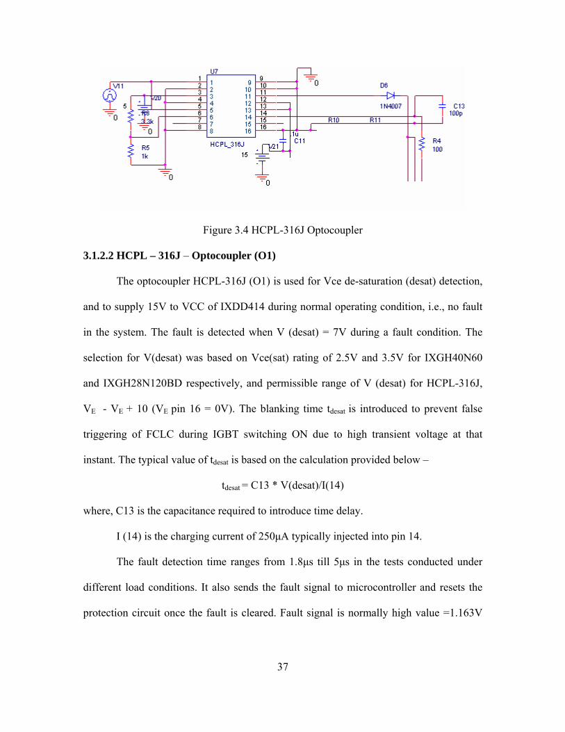
3.1.2.2 HCPL – 316J – Optocoupler (O1)
The optocoupler HCPL-316J (O1) is used for Vce de-saturation (desat) detection,
and to supply 15V to VCC of IXDD414 during normal operating condition, i.e., no fault
in the system. The fault is detected when V (desat) = 7V during a fault condition. The
selection for V(desat) was based on Vce(sat) rating of 2.5V and 3.5V for IXGH40N60
and IXGH28N120BD respectively, and permissible range of V (desat) for HCPL-316J,
VE - VE + 10 (VE pin 16 = 0V). The blanking time tdesat is introduced to prevent false
triggering of FCLC during IGBT switching ON due to high transient voltage at that
instant. The typical value of tdesat is based on the calculation provided below –
tdesat = C13 * V(desat)/I(14)
where, C13 is the capacitance required to introduce time delay.
I (14) is the charging current of 250μA typically injected into pin 14.
The fault detection time ranges from 1.8μs till 5μs in the tests conducted under
different load conditions. It also sends the fault signal to microcontroller and resets the
protection circuit once the fault is cleared. Fault signal is normally high value =1.163V

38
can be adjusted as per requirement because it is dependent on the voltage divider R8 =
3.3kΩ and R5 = 1kΩ shown in Figure 3.4.
Vfault (pin 6) = Vcc (pin 3) * R5/(R8 + R5 )
The moment it goes low (value = 0V) the microcontroller is informed of fault in
the system. The fault is again restored to normally high condition within 6μs of reset
signal going low. The reset signal (pin 5), which is normally high (value = 5V typically),
can be sent by several methods – a) manual, b) auto and c) the microcontroller. In this
thesis manual reset is used once the fault is cleared from the system.
The output of the HCPL-316J through pin 11 supplies the Vcc input to the gate
drive IXDD414. The value of the output is determined by Vcc2 = 15V (pin 12 and 13).
The timing diagram and voltage of Vin for the optocoupler is similar to Vin gate pulse for
IXDD414. The gate pulse for switching the optocoupler is supplied through Vin+ (pin 1)
which is the non-inverting input pin. This implies that the gate drive output voltage will
follow the input voltage. The inverting pin Vin- (pin 2) is grounded. The positive input
voltage Vcc1 is 5V which is within the rated range to 4.5 V -5.5 V.
3.1.2.3 LM317K – Voltage Regulator (U6)
LM317K voltage regulator is used to lower the gate voltage to 9V so as to limit
the fault current. The value can be varied depending on the SOA of the device. The ratio
between R10 and R11 determines the output of the regulator. Input voltage is 15V.
R11
1k
U6LM317K
IN2
OUT3A
DJ
1
R10
8k
Figure 3.5 Voltage regulator model LM317K

39
Figure 3.6 Comparator U1 for Under-Voltage lockout
3.1.2.4 LM311 – Comparator (U1 & U2)
Figure 3.6 represents the gate under-voltage lockout circuit. This feature
safeguards the IGBT from running at gate voltages less than 9V. In case of a device
tested in this thesis, the IGBT will operate in linear region for Vg < 9V which, will result
in rapid heating of DUT resulting in thermal stress. In order to prevent this stress the
under-voltage lockout feature is introduced. This circuit has the dual purpose of
switching off the device during under-voltage as well as short circuit condition. The
inverting terminal of U1 is connected to the Vcc of the gate drive. It is this voltage which
has to be monitored. The reference voltage Vref is set at 9.5V and fed to the non-
inverting terminal of U1. The moment Vcc goes below 9.5V, U1 comes into operation
after a time delay of 5μs introduced by R12 and C5 shown in Figure 3.6. During fault
current limiting, the gate voltage across the device is reduced from 15V to 9V, and then
from 9V to 0V after a delay of 5μs by the RC time delay circuit. This two step turning
OFF of IGBT is termed as soft switching. The di/dt and dv/dt values will be

40
comparatively less than in the case of gate voltage drop of 15V to 0V. Hysteresis is added
by connecting a large resistance R19 between U1’s output and non-inverting terminal.
Hysteresis prevented false triggering of comparator due to noise.
The BJT NPN transistor Q2 is switched on via the comparator U2 output when
the gate voltage goes beyond 16V, thereby switching in the zener diode 1N4744A (D9).
The zener diode D9 shown in Figure 3.7 (a) is used to clamp the gate voltage to 15V
during FUL condition until the desat correction comes into picture. The rating of the
zener diode is 15V, 1W. The triggering voltage for gate over voltage is 16V which sets
the comparator output to high when gate voltage goes beyond 16V. Hysteresis is added
similar to gate under-voltage lockout feature, via, a large resistance R14 of value 100kΩ
between output and non-inverting terminal of U2.

41
(a)
(b)
Figure 3.7 (a) gate over-voltage limiting circuit, (b) Comparator circuit for gate over-
voltage detection

42
U3
HCPL4506
1021
1032
1053
1064
1075
1086
V
U2
IXDD414
VCC1
IN2
EN3
GND4
VCC5
OUT6
OUT7
GND8
C2
1u
V1
AC =TRAN =
DC = 15V
0 0
Z1 IXGH40N60Rg
50
V3
AC =TRAN =
DC = 15V
R5
25
V185
V13R1
300
R2
190
1
0
0
Figure 3.8 Simulation for testing HCPL-4506 and IXDD414 interconnection
3.1.2.5 HCPL-4506 – Optocoupler (O2)
HCPL-4506 optocoupler is used to provide input signal Vin to the IXDD414 gate
drive circuit. Currently it is shown as a Piecewise linear voltage pulse in the PSPICE
simulation circuit of Figure 3.3. It has been separately tested in PSPICE to check its
compatibility with IXDD414 circuit.The results showed it can be used to isolate the
IGBT device from the utility system.
3.2 Uniqueness of proposed FCL and protection circuit
In Chapter 2 several drawbacks were mentioned and claim was made that the fault
current limiting and protection circuit proposed in this thesis will overcome those
drawbacks. The methodology explains the individual circuit components and their role in
protecting the DUT thereby addressing to drawbacks pointed out earlier. Though gate
over voltage problem has been covered to in many papers, the commercially available
gate drives do not possess this feature. By limiting the gate voltage during FUL

43
condition, the effect of miller capacitance can be reduced. The peak fault current seen by
the IGBT will be less in comparison to the values seen without gate over voltage feature.
Soft switching has been incorporated so that the device is not under stress due to sudden
dip in gate voltage from 15V – 0V. Soft switching is achieved in two steps i.e., drop from
15V-9V and after a time lag of 5μs the voltage dips from 9V-0V. This feature will
additionally prevent complete turn OFF of the device when a fault is detected in the
system. If the fault can be mitigated within 5μs then the device can operate normally
thereby safeguarding the normal operation of the modular block. To optimize the number
of components used, the gate under-voltage lockout feature is tied together with the gate
voltage reduction from 9V to 0V feature.
3.3 Summary
This chapter outlines the simulation model in PSPICE simulation of the actual
fault current limiting and protection gate drive circuit for IGBT applications in modular
converter. The basis for selection of devices was illustrated along with the necessary
calculations. The novelty of the circuit was explained which improved the performance
of the FCL and protection circuit.
Based on the methodology explained in this chapter PSPICE simulation was
conducted and the results obtained are shown in the next chapter.

44
CHAPTER 4 – RESULTS
Brief Outline: This chapter describes the results obtained from running the PSPICE
simulation explained in chapter 3. Chapter 4 comprises of two sections illustrating the
IGBT characteristics under HSF and FUL fault conditions. Section 4.1 demonstrates
IGBT characteristics without fault protection circuit, based on simulation circuit
described in section 3.1. Section 4.2 describes IGBT characteristics with fault protection
circuit along with Table 4.1 which compares desat detection time, peak fault current Ic,
and Vce values under different R-L load conditions. The results shown in section 4.2 are
based on the simulation circuit described in section 3.1. The results obtained prove that
the gate drive circuit can effectively limit fault currents within a short period of time
(<3μs) and can safely shut down the IGBT if the fault persists for more than the short
circuit withstand time of IGBT (>10μs).
4.1 IGBT characteristics under fault, without protection circuit
In this section the test results of HSF and FUL fault characteristics of two IGBTs
a) IXGH40N60, and b) IXGH28N120BD is described. It is divided into two sub-sections
namely-
• Fault Under Load condition
• Hard Switched Fault condition
For reference, the test circuit has already been described in Section 3.1.1. Load
condition is R = 100Ω and L = 2μH. From the results, it can be inferred that the test
IGBT sees high fault current of almost 10 times its current rating and if the fault is not
mitigated within 10μs (short circuit fault withstand time) then it would lead to device
destruction.

45
4.1.1 Fault Under Load condition
The IGBTs DUT in both cases Figure 4.1 a) and b) are switched on at t=1ns and
stays on till t=30μs. The IGBT SW is IXGH40N60 in both cases and is switched in order
to create a fault under load condition. The DUTs are exposed to a line voltage of 480V at
t=8μs when another IGBT SW is switched on causing fault under load condition. The
collector current rises to 800A in case a) and 240A in case b). The gate voltage in both
cases goes beyond 16V for a brief period of time of ~ 1μs. The fault remains in the
system for 15μs which is long enough to cause thermal stress on the devices. The
collector current during the fault exceeds the device rating. This will eventually lead to
device failure due to overheating. Vge shown in Figure 4.1 is multiplied by a factor of 10
for ease of comparison with the rest of the parameters.
The gate over-voltage lockout feature has not been incorporated in the circuit for
waveforms shown in Figure 4.1 a) and b). The initial peak fault current is higher in
comparison to a protection circuit with gate over-voltage lockout feature.

46
(a)
(b)
Figure 4.1 Fault under load condition without protection, Vce, Ic and Vge waveform for
a) IGBT IXGH40N60, and b) IGBT IXGH28N120BD

47
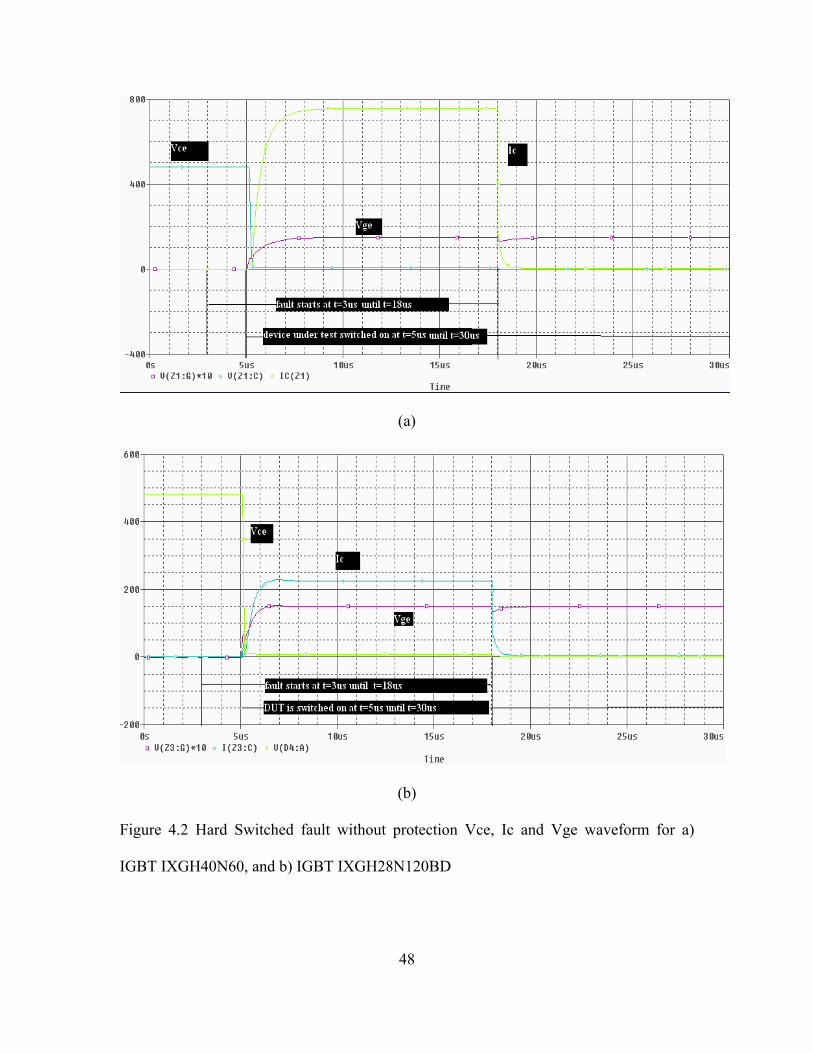
4.1.2 Hard Switched Fault condition
Figure 4.2 a) has DUT IXGH40N60 of rating 600V, 75A and Figure 4.2 b) has
DUT IXGH28N120BD of rating 1200V, 50A. The DUT is switched on at t=5μs and
stays on until 30μs. However, the instant the DUT is switched on it is exposed to the line
voltage of 480V because of the IGBT SW that was switched on at t= 3μs. The DUT is
exposed to HSF and the Ic rises to - 750A (Figure 4.2a) and 230A (Figure 4.2b). The
duration of fault shown here is 13us for the DUT and this again will cause over heating in
the device resulting in device failure over a longer period of time. The effect of Miller
capacitance is less during HSF condition; hence, the peak fault currents seen by the
devices are less in comparison to FUL condition. Vge shown in Figure 4.2 is multiplied
by a factor of 10 for ease of comparison with rest of the parameters.
Figures 4.1 and 4.2 undoubtedly show the need for having a fault current limiting
and protection circuit which will lower the current seen by the device thereby ensuring
longer lifetime and safe operation of IGBTs. In the next section results obtained from the
fault current limiting and protection circuit are analyzed.
48
(a)
(b)
Figure 4.2 Hard Switched fault without protection Vce, Ic and Vge waveform for a)
IGBT IXGH40N60, and b) IGBT IXGH28N120BD

49
4.2 IGBT characteristics under fault, with protection circuit
The results of the fault current limiting and protection gate drive circuit explained
in Section 3.1.2 are analyzed in this section. The thesis is based on the results explained
in the following sub-sections –
• Hard switched fault mitigation with protection circuit
• Fault under load mitigation with protection circuit
The gate drive circuit developed is unique in relation to its treatment to gate over
voltage feature that has been neglected in previous works (Chapter 2). There is also a
choice of not switching OFF the device the instant a fault is detected. The device stays
ON for a short period of 5μs, and in case the fault gets cleared within this short time, then
the device can resume its normal operation. The device switch OFF is done in two steps
i.e., reducing gate voltage from 15V – 9V followed by 9V- 0V after a time lag of 5μs.
This two step switching is termed as soft switching as the di/dt and dv/dt seen by the
device will be comparatively less than that seen during a 15V-0V drop. This feature
further improves the functionality of the protection circuit. The time lag between the two
steps can be adjusted depending upon device withstand capacity. The under voltage
lockout and soft switching of 9 to 0V is combined together in order to minimize the
number of components used in the protection gate drive circuit.

50
4.2.1 Hard switched fault with protection circuit
The DUT in Figure 4.3 a) is IXGH40N60 and in Figure 4.3 b) is
IXGH28N120BD. In both cases the DUT is switched on at t=5μs and is exposed to HSF
condition. Since Vce picks up from 0V, the Vce desat detection takes time t= 4 μs from
t1 until t2. At time t3 = 14.5μs (case a), or t3 = 14μs (case b) the device is switched OFF
as the fault condition prevails for more than 9μs. There is a two step reduction in gate
voltage so as to prevent large L di/dt which would result in a voltage surge across Vce. At
t2 = 9.5μs (case a), or t2 =9μs (case b) the gate voltage is reduced to 9V with the help of
LM317K voltage regulator. This stays at 9V for another 5μs (time can be varied
depending on device characteristics i.e., how long can it sustain operation at gate voltage
of 9V) before reducing it to 0V so as to switch OFF the device at t3= 14.5μs (case a), or
t3 = 14μs (case b). At t=18μs the fault is removed from the system and the device is
safely switched on at t4=25.3μs (case a), or t4 = 24.8μs (case b) by resetting the fault
correction circuit. Because the gate voltage remains within 16V, the gate over voltage
clamping circuit does not come into operation in HSF. The peak current seen across DUT
in case a) is 750A, and b) is 250A.

51
(a)
(b)
Figure 4.3 Hard switched fault with protection, Vce, Ic and Vge characteristics, a) DUT
is IXGH40N60, and b) DUT is IXGH28N120BD

52
4.2.2 Fault under load condition with protection circuit
The DUT in Figure 4.4 a) is IXGH40N60 and in Figure 4.4 b) is
IXGH28N120BD. In both cases DUT is switched on at t=1ns and stays on until 30μs,
fault occurs at t1=8μs and remains until 23μs. The fault current limiting and soft
switching OFF of DUT is similar to HSF. The fault current limiting starts at t2=10μs and
at t3=15μs i.e., 5μs later the device is safely switched OFF. The fault is removed after
15μs i.e., at time t=23μs, after which the device resumes its normal switching state at
t4=24.8μs. However, in FUL the gate voltage rises above 15V, this causes an increase in
the fault current seen by the device. The Miller capacitance across the gate and collector
Cgc can cause high current across the IGBT gate-collector Igc = Cgc dv/dt, causing rise
in Vge. A gate voltage clamping circuit is used comprised of comparator LM311 (U2),
NPN transistor Q2N1420 (Q2) and zener diode 1N4744A (D9). The zener diode
clamping circuit is not very popular, however, in this case the voltage clamping is used
for 2μs, after which the two step voltage soft switching comes into action. Hence, the
protection is not solely dependent on the zener diode clamping circuit. The Ic difference
with and without over-voltage protection is approximately 100 A; this is liable to change
depending on the load conditions and line voltage. Reduction in gate voltage causes a
decrease in peak current seen by the device during FUL condition. Figure 4.5 a) and b)
show Vge characteristics in FUL condition without and with gate over voltage protection
respectively.

53
(a)
(b)
Figure 4.4 Fault under load with protection, Vce, Ic and Vge characteristics a) DUT is
IXGH40N60, and b) DUT is IXGH28N120BD

54
(a)
(b)
Figure 4.5 Gate Voltage Vge characteristic a) without over-voltage protection, and b)
with over-voltage protection

55
As seen in the Figure 4.5 (b) the gate voltage is reduced within 0.5μs of Vge
rising above 16V. A small amount of hysteresis is added to the comparator circuit so as to
prevent noise/transient detection which would result in false triggering of comparator U2.
In the under-voltage lockout circuit, a separate LM311 (U1) comparator is used to
trigger the device switching off. The inverting terminal of LM311 is connected to the Vcc
of IXDD414 and the non-inverting terminal is set at 9.5V. In this circuit, a delay of 5μs is
incorporated, i.e., after 5μs of Vcc going below 9.5V the comparator output will go high
and switch on the transistor Q4 to reduce the gate voltage to 0V.
4.2 Observations made under varying R-L load conditions
Table 4.1 Tdesat and Peak fault current for DUT during HSF, varying load R-L
Serial No
L in H
R in Ω
Tdesat in μs IXGH40N60
Ic peak in A IXGH40N60
Tdesat in μs IXGH28N120BD
Ic Peak in A IXGH28N120BD
1 20 4.5 760 4 250
2 50 4.5 750 4 250
3
20n
100 4.5 750 4 248
4 20 4.5 760 4 250
5 50 4.5 760 4 250
6
2u
100 4.5 750 3.9 250
7 20 4.5 760 4 250
8 50 4.5 750 4 250
9
10u
100 4.5 750 3.9 248

56
Table 4.2 Tdesat and Peak fault current for DUT during FUL, varying load R-L
Serial No
L in H
R in Ω
Tdesat in μs IXGH40N60
Ic peak in A IXGH40N60
Tdesat in μs IXGH28N120BD
Ic Peak in A IXGH28N120BD
1 20 2 755 1.5 250
2 50 2 750 1.5 250
3
20n
100 2 750 1.5 250
4 20 2 750 1.5 250
5 50 2 755 1.5 250
6
2u
100 2 750 1.5 250
7 20 2 755 1.5 250
8 50 2 750 1.5 250
9
10u
100 2 750 1.5 250
Table 4.1 and 4.2 show desat detection time taken to detect a fault in the circuit
and the peak fault current under several R and L combinations. Observations show that
there is little effect of varying load over the desat detection and peak fault current which
should be the case. Hence, the fault current limiting and protection circuit will work
efficiently irrespective of load condition.
4.3 Summary
In this chapter the results obtained proved the working of fault current limiting
circuit proposed in this thesis. The uniqueness of the circuit has been explained with the
help of waveforms. In the next chapter conclusion drawn from the thesis is illustrated
along with scope of future improvements.

57
CHAPTER 5: CONCLUSION AND FUTURE WORK
Brief Outline: This chapter presents the conclusions drawn from the project and the
possible future work that would enhance the performance of fault current limiting and
protection circuit in Section 5.2.
5.1 Conclusions
In order to safeguard power electronics used in FACTS applications, a fault
current limiting and protection circuit should be provided working independent of the
gate drive circuit. The system level fault mitigation assemblies take long time to remove
a fault, and within this time the IGBTs used in the FACTS application will undergo high
thermal and mechanical stress. Exposure to such conditions over a prolonged period of
time will reduce the device lifetime, which is one of the major reasons why power
electronics are very popular in utility applications.
Modular converter approach will reduce the device ratings required to mitigate
the fault in power electronics. The modular block operated at 480V voltage level is not
very high in comparison to 1000s of volts for STATCOM application. Hence, the ease of
introducing the FCL and protection circuit along with redundancy, localized control etc,
illustrated in section 1.2 are some of the reasons behind growth in research of modular
converter applications.
Different fault current limiting circuits are discussed in Chapter 2. The inherent
features that FCLC should possess are described. The various detection techniques to
detect a fault across IGBT are discussed along with proposing the most commonly used
technique Vce desat detection for quick detection of fault. The FCLC used in motor
drive, STATCOM, and modular converter applications are described. The features and

58
drawbacks of each circuit are explained, hence, leading to a novel FCL and protection
circuit for IGBTs used in a modular converter. The circuit proposed in this thesis is based
on the desired features of FCLC enumerated in Chapter 2.
Chapter 3 defines the methods employed in developing the fault current limiting
and protection circuit. The simulation tool used is PSPICE, the choice was made based on
its vast components library. A simple test circuit is developed comprised of an IGBT that
is a device under test and a switch to introduce hard switch fault and fault under load
conditions for device testing. Different timing pulses are fed to each IGBT to get the
desired results. First the test circuit is simulated without a protection circuit in order to
observe the effect of fault on the DUT. The results obtained confirmed the need to have a
fault current limiting and protection circuit as the DUT saw high fault currents beyond
the range of device rating. In real world scenario, the high fault currents would definitely
lead to device destruction due to overheating.
The test circuit is then simulated with the fault current limiting and protection
circuit. Section 3.1.2 describes the choice of components based on device ratings like
temperature, voltage, and current range. The load conditions were varied over a range of
R-L combinations to test the effect of load conditions on the protection feature of gate
drive circuit. The FCL and protection circuit proposed entails the features not considered
in previous work done in this area. Though gate over voltage problem has been addressed
in many papers, the commercially available gate drives do not possess this feature. By
limiting the gate voltage during FUL condition the effect of Miller capacitance can be
reduced. The peak fault current seen by the IGBT will be less in comparison to the values
seen without gate over voltage feature. Soft switching has been incorporated so that the

59
device is not under stress due to sudden dip in gate voltage from 15V – 0V. Soft
switching is achieved in two steps i.e., drop from 15V-9V, and after a time lag of 5μs the
voltage dips from 9V-0V. This feature will additionally prevent complete turn OFF of the
device when a fault is detected in the system. If the fault can be mitigated within 5μs,
then the device can operate normally, thereby safeguarding the normal operation of the
modular block. To optimize the number of components used, the gate under voltage
lockout feature is tied together with the gate voltage reduction - 9V to 0V feature.
The waveforms described in Section 4.2 validate the working of fault current
limiting and protection circuit. The entire operation of fault detection and current limiting
feature enabling was done within 4μs for HSF and 2 μs for FUL conditions. The time
required to detect a fault in HSF was more than that required in FUL because of Vdesat
ramping from 0V-7V in HSF and Vce (ON)-7V in FUL. Vce (ON) for devices used in
this thesis are IXGH40N60 2.5V, IXGH28N120BD 3.5V. The fault signal goes low when
a fault was detected by the Vdesat detection feature and stays low until reset signal is
enabled. After the fault was cleared a reset signal was sent manually to the optocoupler
HCPL-316J in order to reset the entire fault protection circuit. This brought the protection
circuit back to its normal operating condition. The fault signal is tied to the reset signal
hence after 6μs it returns to normally high value.
5.2 Future Work
Temperature lockout feature could not be added to the FCL and protection circuit.
In order to improve the gate drive circuit the temperature lockout feature has to be
included. This will protect the IGBT from overheating by setting reference temperature
(Tref). When device temperature exceeds the Tref the IGBT will be safely switched OFF

60
to prevent device destruction. Due to absence of thermal sensors in PSPICE components
library, this feature was not included in the simulation model.
Furthermore, the simulation model has to be tested in hardware before testing it
with an actual modular block model. Though PSPICE simulation is closest to real time
applications, it does not guarantee 100% accuracy.
5.3 Summary
This chapter presents the overview of the thesis and the conclusion drawn from
the simulation model. Future work to enhance the features of fault current limiting and
protection circuit has been proposed. Future work also includes testing of circuit in
hardware.

61
REFERENCES

62
[1] M. Trivedi, V. John, T.A. Lipo and K.Shenai, “Internal dynamics of IGBT under fault
current limiting gate control,” IEEE-IAS Conf. Rec., 2000, pp.2903-2908.
[2] R. Chokhawala and G. Castino, “IGBT fault current limiting circuit,” IEEE-IAS Conf.
Rec., 1993, pp.1339-1345.
[3] V. John, B. S. Suh and T. A. Lipo, “Fast-clamped short circuit protection of IGBTs,”
IEEE Trans. Ind. Appl., vol. 35, no. 2, pp. 477-486, 1999.
[4] R. Chokhawala, J Catt and L Kiraly, “A discussion on IGBT short-circuit behavior
and fault protection schemes,” IEEE Trans. Ind. Appl., vol. 31, Issue 2, March-April
1995, pp. 256-263.
[5] R. Pagano and A. Raciti, “Evolution in IGBT's protection against short circuit
behaviors by gate-side circuitry,” Proceedings of the 2002 IEEE International
Symposium on Industrial Electronics., vol. 3, 26-29 May 2002, pp. 913-918.
[6] S. Tomoyuki, M. Ishiko, S. Kawaji, T. Sugiyama, K. Hotta, T. Fukami and K.
Hamada, “Investigation of Short-circuit Capability of IGBT under High Appliead
Voltage Conditions,” R&D Review of Toyota CRDL, vol. 39 No. 4, pp 22-26.
[7] K.J Um, “Fairchild Semiconductor Application Note 9020 IGBT Basic II,” Rev. A,
April 2002.
[8] K. Fuji, A. Suzuki, S. Konishi, J. Takazane, M. Ohki, M. Daiguji, “STATCOM
Applying Flat-Packaged IGBTs Connected In Series,” 35th Annual IEEE Power
Electronics Specialists Conference, 2004, Germany.
[9] “Using Intelligent Power Module”, Mitsubishi Semiconductors Power Modules,
September 1998.

63
[10] Wei Liu, “Distributed Modular Controller Architecture For High Power Converter
Applications,” Master’s Thesis at North Carolina State University, 2005.

64
Vita
Shibani Mishra was born on 12th January, 1983, in Rourkela, India. She studied in
Rourkela until her B.Tech. She obtained her Bachelors in Technology degree in Electrical
Engineering from National Institute of Technology, (formerly known as Regional
Engineering College) Rourkela. She graduated in May 2005 with Honors. She worked for
a year with IT giant Infosys Technologies Limited. She joined University of Tennessee,
Knoxville to pursue her Master’s degree in Electrical Engineering. She worked on her
thesis supervised Dr. Leon M Tolbert. She developed a simulation model for “fault
current limiting and protection circuit for power electronics used in modular converter”.
During her masters she worked as a Graduate Assistant with Innovative Technology
Center and was involved in its visual design team.