to download/view this file - universiteit stellenbosch
TRANSCRIPT

UNIVERS ITE IT •STELLENBOSCH •UNIVERS ITY
j ou kenn i s v ennoo t • you r know ledge pa r tne r
The Design of a CMOS Sensor Camera System
for a Nanosatellite
by
Eric Albert Baker
Thesis presented in partial fullment of the requirements for
the degree of Master of Electronic Engineering with
Computer Science at the University of Stellenbosch
Department of Electric and Electronic EngineeringUniversity of Stellenbosch
Private Bag X1, 7602 Matieland, South Africa
Supervisor: Prof P.J. Bakkes
October 2006

Declaration
I, the undersigned, hereby declare that the work contained in this thesis is my own
original work and that I have not previously in its entirety or in part submitted it
at any university for a degree.
Signature: . . . . . . . . . . . . . . . . . . . . . . . . . . . . .
E.A. Baker
Date: . . . . . . . . . . . . . . . . . . . . . . . . . . . . . . . . . .
i

Abstract
The Design of a CMOS Sensor Camera System
for a Nanosatellite
E.A. Baker
Department of Electric and Electronic Engineering
University of Stellenbosch
Private Bag X1, 7602 Matieland, South Africa
Thesis: MScEng (Electric and Electronic with Computer Science)
October 2006
This thesis relates to the design of a camera system for a nanosatellite based on
a CMOS image sensor. The design specications and constraints are considered
followed by the proposal of a versatile design with all the required functions imple-
mented on a single FPGA. These functions include bad block management, data
routing, an EDAC, a soft-core processor, glue logic to external devices, and com-
munication busses.
The Altera Nios II soft-core processor is implemented in this design, which en-
ables simple changes to be made in software. A good mixture of intellectual prop-
erty soft-cores, open-source cores, and user created logic are utilised in this broad
base design, containing a combination of hardware, digital logic, and software.
Low power and compact devices are selected for this design to minimize the
power usage and the physical size of the camera system. The system's peak power
consumption is 952mW which is below the required maximum consumption of 1W .
This design's performance is therefore ideal for a subsystem onboard a nanosatel-
lite.
ii
Uittreksel
Die Ontwerp van 'n CMOS Sensor Kamerastelsel
vir 'n Nanosatelliet
(The Design of a CMOS Sensor Camera System
for a Nanosatellite)
E.A. Baker
Departement Elektries en Elektroniese Ingenieurswese
Universiteit van Stellenbosch
Privaatsak X1, 7602 Matieland, Suid Afrika
Tesis: MScIng (Elektries en Elektronies met Rekenaarwetenskap)
Oktober 2006
Hierdie tesis handel oor die ontwerp van 'n kamerastelsel vir 'n nanosatelliet ge-
baseer op 'n CMOS beeld sensor. Die ontwerp spesikasies en beperkings word
ondersoek, gevolg deur die voorstel van 'n buigbare ontwerp wat al die verlangde
funksies implementeer op 'n enkele FPGA. Hierdie funksies behels die bestuur van
defektiewe geheuesegmente, data verskuiwing, foutopsporing en -herstel, 'n sagte-
kern verwerker, verbindingslogika na eksterne toestelle en kommunikasie busse.
Die Altera Nios II sagte-kern verwerker is toegepas in hierdie ontwerp, wat
toelaat dat eenvoudige veranderinge in sagteware aangebring kan word. 'n Goeie
versameling van intellektuele eiendom sagte-kerne, oopgestelde bronkode kerne en
gebruiker-geskepte logika word gebruik in hierdie omvattende ontwerp wat bestaan
uit 'n kombinasie van hardeware, digitale logika en sagteware.
Lae kragverbruik- en kompakte komponente word vir hierdie ontwerp gekies om
kragverbruik en die siese grootte van die kamerastelsel te minimeer. Die stelsel se
iii

UITTREKSEL iv
piek kragverbruik is 952mW wat minder is as die verlangde maksimum kragverbruik
van 1W .
Die ontwerp se werkverrigting is dus ideaal vir 'n substelsel aan boord van 'n
nanosatelliet.

Acknowledgements
I would like to express my sincere gratitude to the following people:
Professor P.J. Bakkes (thesis supervisor) for his support and interest in the
project,
Johan Grobbelaar for the PCB layout,
Liza Baker and Johan Schoonwinkel for taking time out of their busy schedules
to proof read this document,
Johannes, Janto and Gerrit who were always willing to give advice.
v

Dedications
Hierdie tesis word opgedra aan my familie,
vir hulle ondersteuning, liefde en gebede.
vi

Contents
Declaration i
Abstract ii
Uittreksel iii
Acknowledgements v
Dedications vi
Contents vii
List of Figures x
List of Tables xii
List of Abbreviations and Symbols xiii
1 Introduction 1
1.1 Aims and Objectives . . . . . . . . . . . . . . . . . . . . . . . . . . 2
1.2 The Rest of the Document . . . . . . . . . . . . . . . . . . . . . . . 3
2 Background 5
2.1 Nanosatellites . . . . . . . . . . . . . . . . . . . . . . . . . . . . . . 5
2.2 Kodak KAC-1310 CMOS Image Sensor . . . . . . . . . . . . . . . . 7
2.3 NAND Flash Memory . . . . . . . . . . . . . . . . . . . . . . . . . 11
2.4 Altera Nios II . . . . . . . . . . . . . . . . . . . . . . . . . . . . . . 15
2.5 Communication Methods . . . . . . . . . . . . . . . . . . . . . . . . 18
vii

CONTENTS viii
3 Design Specications 22
3.1 Design Constraints . . . . . . . . . . . . . . . . . . . . . . . . . . . 23
4 System Design Overview 32
4.1 FPGA Considerations . . . . . . . . . . . . . . . . . . . . . . . . . 32
4.2 VHDL Design Overview . . . . . . . . . . . . . . . . . . . . . . . . 34
4.3 Design Implementation Changes . . . . . . . . . . . . . . . . . . . . 45
5 Detailed System Design 46
5.1 VHDL Design Detail . . . . . . . . . . . . . . . . . . . . . . . . . . 46
5.2 Nios II and Components Design . . . . . . . . . . . . . . . . . . . . 58
5.3 Hardware Design . . . . . . . . . . . . . . . . . . . . . . . . . . . . 67
6 Simulations and Results 77
6.1 VHDL Simulations . . . . . . . . . . . . . . . . . . . . . . . . . . . 77
6.2 Nios II Simulations and Measurements . . . . . . . . . . . . . . . . 89
6.3 Kodak KAC-1310 Interfacing . . . . . . . . . . . . . . . . . . . . . 90
6.4 Demonstration Board Testing and Measurements . . . . . . . . . . 93
6.5 Work in progress . . . . . . . . . . . . . . . . . . . . . . . . . . . . 95
7 Conclusions and Recommendations 96
7.1 Conclusions . . . . . . . . . . . . . . . . . . . . . . . . . . . . . . . 96
7.2 Recommendations . . . . . . . . . . . . . . . . . . . . . . . . . . . . 98
List of References 99
Appendices 102
A Kodak KAC-1310 Datasheet 103
B Samsung K9K4G08U0M Datasheet 105
C imageexporter_regs.h 107
D image_exporter_avalon_interface.vhd 109
E cmosimager.c 114

CONTENTS ix
F Demonstration Board Schematics 117
G Power Regulators 123
G.1 National Semiconductor LM2651 . . . . . . . . . . . . . . . . . . . 123
G.2 ST LF25CPT . . . . . . . . . . . . . . . . . . . . . . . . . . . . . . 123
G.3 Texas Instuments SN105125 . . . . . . . . . . . . . . . . . . . . . . 123

List of Figures
1.1 Block Diagram of a possible Nanosatellite . . . . . . . . . . . . . . . . 2
2.1 Block Diagram of a Proposed Camera Design . . . . . . . . . . . . . . 6
2.2 Bayer RGB Pattern CFA . . . . . . . . . . . . . . . . . . . . . . . . . . 9
2.3 Bayer CMY Pattern CFA . . . . . . . . . . . . . . . . . . . . . . . . . 9
2.4 Samsung K9K4G08U0M Memory Array Organisation . . . . . . . . . . 12
2.5 Write Data & Read Status Operation . . . . . . . . . . . . . . . . . . . 13
2.6 Read Data Operation . . . . . . . . . . . . . . . . . . . . . . . . . . . . 13
2.7 Block Erase Operation . . . . . . . . . . . . . . . . . . . . . . . . . . . 14
2.8 Example of a Nios II Processor System . . . . . . . . . . . . . . . . . . 16
3.1 Single Frame Capture Mode (SFRS) . . . . . . . . . . . . . . . . . . . 23
3.2 Default Row Sync Waveforms . . . . . . . . . . . . . . . . . . . . . . . 25
3.3 NAND ash page write sequence . . . . . . . . . . . . . . . . . . . . . 27
4.1 System Block Diagram . . . . . . . . . . . . . . . . . . . . . . . . . . . 34
4.2 Dual Clock FIFO . . . . . . . . . . . . . . . . . . . . . . . . . . . . . . 35
4.3 Data Router with EDAC Block Diagram . . . . . . . . . . . . . . . . . 37
4.4 NAND Flash Memory Interface Block Diagram . . . . . . . . . . . . . 38
4.5 An Example of the proposed Bad Block Table organisation . . . . . . . 39
4.6 Bad Block Table & Address Manager Block Diagram . . . . . . . . . . 41
5.1 Bad Block Table & Address Manager Flow Chart . . . . . . . . . . . . 48
5.2 Valid Block Address Generation Flow Chart . . . . . . . . . . . . . . . 51
5.3 The Nios II based camera system in SOPC Builder . . . . . . . . . . . 60
5.4 Nios II system integrating an EPCS Controller . . . . . . . . . . . . . . 61
5.5 I2C Module's Avalon slave timing conguration . . . . . . . . . . . . . 65
x

LIST OF FIGURES xi
5.6 CMOS Image Sensor Interface's Avalon slave timing conguration . . . 66
5.7 Image Exporter's Avalon slave timing conguration . . . . . . . . . . . 67
5.8 JTAG Indirect Conguration Device Programming . . . . . . . . . . . 68
5.9 Termination Scheme on Cyclone II LVDS Transmitter . . . . . . . . . . 71
5.10 Altera MegaWizard generated PLL with Locked signal output . . . . . 72
5.11 Design routing and layout - Top layer . . . . . . . . . . . . . . . . . . . 76
5.12 Design routing and layout - Bottom layer . . . . . . . . . . . . . . . . . 76
6.1 Load Bad Block Table Waveforms, Segment 1 . . . . . . . . . . . . . . 79
6.2 Load Bad Block Table Waveforms, Segment 2 . . . . . . . . . . . . . . 80
6.3 Block Diagram of Image Exporter with Simulation signal names . . . . 81
6.4 Store Bad Block Table Waveforms, Segment 1 . . . . . . . . . . . . . . 83
6.5 Store Bad Block Table Waveforms, Segment 2 . . . . . . . . . . . . . . 84
6.6 Store Bad Block Table Waveforms, Segment 3 . . . . . . . . . . . . . . 85
6.7 Store Bad Block Table Waveforms, Segment 4 . . . . . . . . . . . . . . 86
6.8 Erase All Sequence Waveform . . . . . . . . . . . . . . . . . . . . . . . 88
6.9 Avalon access times to CMOS Image Sensor Interface Module . . . . . 91
6.10 Sub-sampled photo taken with the camera system (160×100 pixels) . . 92
A.1 Kodak KAC-1310 CMOS Image Sensor Datasheet, Page 5 . . . . . . . 104
B.1 Samsung K9K4G08U0M NAND Flash Datasheet, Page 2 . . . . . . . . 106
F.1 Design Schematic Page 1 . . . . . . . . . . . . . . . . . . . . . . . . . . 118
F.2 Design Schematic Page 2 . . . . . . . . . . . . . . . . . . . . . . . . . . 119
F.3 Design Schematic Page 3 . . . . . . . . . . . . . . . . . . . . . . . . . . 120
F.4 Design Schematic Page 4 . . . . . . . . . . . . . . . . . . . . . . . . . . 121
F.5 Design Schematic Page 5 . . . . . . . . . . . . . . . . . . . . . . . . . . 122
G.1 National Semiconductor LM2651 Datasheet, Page 1 . . . . . . . . . . . 124
G.2 ST LF25CPT Datasheet, Page 1 . . . . . . . . . . . . . . . . . . . . . 125
G.3 Texas Instruments SN105125 Datasheet, Page 1 . . . . . . . . . . . . . 126

List of Tables
2.1 Bus state with two nodes transmitting simultaneously . . . . . . . . . . 21
3.1 Readout Times compared to MCLK . . . . . . . . . . . . . . . . . . . 24
3.2 Data Rates compared to MCLK . . . . . . . . . . . . . . . . . . . . . . 25
3.3 NAND Flash Burst and Continuous Write Data Rates . . . . . . . . . 27
5.1 Nios II Processor Conguration . . . . . . . . . . . . . . . . . . . . . . 59
xii

List of Abbreviations and Symbols
µs microsecond
ms millisecond
ns nanoseconds
A Ampere, SI-unit for electric current
ADC Analogue to Digital Converter
ALE Address Latch Enable signal
ANSI C American National Standards Institute C programming language
API Application Program Interface
AS Active Serial
ASDI AS Data Input
ASIC Application Specic IC
AWB Auto White Balance
BGA Ball-Grid Array
CAN Controller Area Network
CFA Colour Filter Array
CISC Complex Instruction Set Computer
CLK Clock
CMOS Complementary Metal Oxide Semiconductor
CMY Cyan, Magenta, Yellow
CPU Central Processing Unit
CSMA/BA Carrier Sense Multiple Access/Bitwise Arbitration
DCLK Data Clock
xiii

LIST OF ABBREVIATIONS AND SYMBOLS xiv
DMIPS Dhrystone MIPS
DPGA Digitally Programmable Ampliers
ECC Error Checking and Correcting
EDAC Error Detection and Correction
EEPROM Electrically Erasable Programmable Read Only Memory
EPCS Altera family signature on a part number that refers to serial cong-
uration devices.
EPROM Erasable Programmable Read Only Memory
ESL Electronic Systems Laboratory
FFT Fast Fourier Transform
FIFO First-in First-out
FPGA Field Programmable Gate Array
HAL Hardware Abstraction Layer
HCLK Horizontal Clock
HDL Hardware Description Language
Hz Hertz = per second
I2C Inter-Integrated Circuit
IC Integrated Circuit
IDE Integrated Development Environment
IP Intellectual Property
JTAG Joint Test Action Group
k kilo = 103
LED Light Emitting Diode
LEO Low Earth Orbit
LSB Least Signicant Bit
M Mega = 106
Mb Megabit
MB Megabyte
MCLK Master Clock

LIST OF ABBREVIATIONS AND SYMBOLS xv
MHz Mega Hertz
MIPS Million Instructions per Second
MMU Mass Memory Unit
MSB Most Signicant Bit
MSEL Mode Select
NAND Not AND logic operation
OBC On-Board Computer
OR A Boolean logic operation that is true if any of the inputs are true.
PC Personal Computer
PCB Printed Circuit Board
PLL Phase Locked Loop
QFP Quad Flat Pack
RAM Random Access Memory
RE Read Enable signal
RF Radio Frequency
RGB Red, Green, Blue
RISC Reduced Instruction Set Computer
ROM Read Only Memory
SCL Serial Clock signal
SDA Serial Data signal
SERDES Serializer/Deserializer
SOF Start Of Frame
SOPC System On a Programmable Chip
SRAM Static RAM
SUNSAT-1 Stellenbosch UNiversity's 1st SATellite
SXGA Super Extended Graphics Array
UART Universal Asynchronous Receiver Transmitter
V Volt
VCLK Vertical Clock

LIST OF ABBREVIATIONS AND SYMBOLS xvi
VHDL VHSIC Hardware Description Language
VHSIC Very High-Speed Integrated Circuit
VTU Video Data Transmission Link
XOR Exclusive OR

Chapter 1
Introduction
The Electrical and Electronic Engineering department at Stellenbosch University
has been designing and building low earth orbit (LEO) satellites since 1991. The
rst satellite, SUNSAT-1 (Stellenbosch University Satellite), was launched in 1999.
This was also South Africa's rst satellite.
The Electronic Systems Laboratory (ESL) was established to serve as a facility
where SUNSAT-1 could be designed and built, and also for continuing satellite
research. Following the success of the rst satellite, engineers at Stellenbosch have
been involved with designing new satellites and doing further research.
Currently post-graduate engineers at Stellenbosch University are developing a nano-
satellite. The main purpose of the nanosatellite project is to train engineers using
practical experience by facilitating their involvement in an elite and exhilarating
real-world application.
Nanosatellite missions have the advantage that state-of-the-art instruments can be
tested since these satellites are manufactured on a short time scale and at low cost.
This is not only ideal for science but also for instrument testing and education.
Designing a new, small and low power camera system for the nanosatellite ts
perfectly into this scenario.
1

CHAPTER 1. INTRODUCTION 2
1.1 Aims and Objectives
The main objective of this thesis is to design a small, low power camera system
for a nanosatellite. Figure 1.1 shows a possible subsystem conguration onboard a
nanosatellite and illustrates the integration of a camera into the satellite system.
The camera system communicates with the On-board Computer (OBC) via the
Figure 1.1: Block Diagram of a possible Nanosatellite
CAN bus. Images are stored in the Mass Memory unit (MMU) and downloaded to
the Video Data Transmission (VTU) Modem with a LVDS connection. The VTU
Modem transmits the images to the ground station with a RF link.

CHAPTER 1. INTRODUCTION 3
A Kodak KAC-1310 Image Sensor is supplied to be integrated into this camera
system. This project will concentrate on acquiring images from this sensor and
storing them in a suitable mass memory. Versatility and upgradeability will be a
key concern of the design as the nal specications and requirements for the camera
are uncertain at the time of design.
This camera system is not intended as a fully functional prototype, but as a demon-
stration of the small size, power usage and versatility of the camera design. These
factors are considered in all design decisions of the thesis.
1.2 The Rest of the Document
Chapter 2 briey discusses the concept of a nanosatellite and why a CMOS im-
age sensor is well suited for a camera application onboard a nanosatellite. The
KAC-1310 CMOS Image Sensor is then discussed in more detail and various inter-
polation algorithms are mentioned. This is followed by an explanation on the basic
operations of NAND ash memory. The concept of invalid blocks in these devices
is also introduced. The Altera Nios II is discussed giving a brief overview of what
soft-core processors entail. Finally, this chapter concludes by briey giving some
background information on communication protocols used in the design.
Chapter 3 looks more closely at the design specications and investigates the various
design constraints. Preliminary calculations on data rate requirements are made
and problems associated with designing components for nanosatellites are discussed.
In Chapter 4, important design decisions are made and a proposed architecture
for the nal design is given. The selection of a FPGA is argued and the intended
functionality of each VHDL component is explained. Changes to the initial design
requirements are also addressed.
Chapter 5 looks in detail at the VHDL design for the demonstration camera. The
hardware design and implementation is discussed and an embedded soft-core pro-
cessor is congured.

CHAPTER 1. INTRODUCTION 4
Chapter 6 shows the results and simulations for the system design. The VHDL
system design is simulated before the PCB is built. The PCB is built and checked
and minor mistakes are discussed. A power analysis of the board and a discussion
on work in progress concludes the chapter.
Chapter 7 is the nal chapter of the thesis with conclusions that were drawn from
the project. Proposals for future studies and suggestions to improve the design are
given.

Chapter 2
Background
2.1 Nanosatellites
A nanosatellite is dened as a satellite weighing in the range of 1kg and 10kg.
Smaller and lighter nanosatellites require smaller and cheaper launch vehicles and
are occasionally launched in multiples. They can also be piggyback launched, using
excess capacity on larger launch vehicles.
Furthermore, since the overall cost risk in the mission is much lower, more up to
date but less space proven technology can be incorporated into nanosatellites than
can be used in larger, more expensive missions.
2.1.1 Application signicance
Cost is not the only reason for the use of miniaturised satellites. Miniaturised
satellites can accomplish missions that larger satellites are unsuitable for, such as:
Constellations for low data rate communications,
Using formations to gather data from multiple points,
5

CHAPTER 2. BACKGROUND 6
In-orbit inspection of larger satellites, and
Experimenting with new, less space proven technology.
2.1.2 Power & Physical constraints
The smaller dimensions of a nanosatellite infer less area for solar panels and thus
less power is generated for the satellite to operate from. Therefore, any component
used on the nanosatellite must be extra small and use power conservatively. Various
methods of reducing power consumption exist. A widely used method to reduce the
average power consumption is duty cycling of all components not requiring constant
power [1]. Another simple method is to slow down operating clock frequencies on
the satellite's subsystems.
The use of low power devices also aids in reducing power usage. Subsystems like
cameras, see Figure 2.1, can use CMOS Image sensors. These sensors use low power
and virtually no external components are needed. Research done at the ESL [2][3]
suggests using NAND ash memory for the mass memory unit. NAND ash is a
non-volatile, high-density memory, which uses very low power and is manufactured
in small, lightweight packages.
Figure 2.1: Block Diagram of a Proposed Camera Design

CHAPTER 2. BACKGROUND 7
2.2 Kodak KAC-1310 CMOS Image Sensor
2.2.1 Device Description
The Kodak KAC-1310 is a SXGA format pixel array, solid state CMOS sensor, with
1280x1024 active elements. The pixels have a 6.0µm pitch. The pinned photodiode
architecture utilized in the pixels ensures high sensitivity and low noise.
The complete analogue image acquisition, digitising, and digital signal processing
of the image is integrated on the device. A 10-bit ADC converts the analogue data
to a 10 bit digital word stream.
A monochrome version image sensor without microlenses is available, but to further
enhance sensitivity an image sensor with Bayer (RGB or CMY) patterned Colour
Filter Array (CFA) microlenses can be used. See Figure 2.2 and Figure 2.3. Auto
White Balance (AWB) as well as exposure gain adjustment can be corrected in real
time with Digitally Programmable Ampliers (DPGAs).
Integrated timing and programming controls allow video or still image capture in
progressive scan modes. A progressive scan camera processes all the lines in order,
row by row, thus no interlacing of lines takes place. Frame rates are programmable
while keeping the Master Clock (MCLK) frequency constant. The sensor outputs
the valid frame, line, and pixel synchronisation signals needed to capture the im-
ages.
The image size is fully programmable to a user-dened window of interest (WOI).
Reduced resolution can be obtained by sub-sampling, while still maintaining a
constant eld of view. The eld of view is the part of the observable world that is
seen at any given moment.
The sensor is controlled by a two-line I2C-compatible serial interface. See Section
2.5.1. The device operates from a single 3.3V power supply and no additional biases
are required. A single Master Clock is necessary for operation. The Master Clock
can range from 1 to 20 MHz.

CHAPTER 2. BACKGROUND 8
2.2.2 Operation
The KAC-1310 sensor consists of a 1280 × 1024 pixel array. The fundamental
operation of a pixel relies on the photoelectric eect where a physical property of
silicon allows it to detect photons of light. The photons produce electron-hole pairs
in the silicon, which are directly in proportion to the intensity and wavelength of
the incident illumination. By applying an appropriate bias, the electrons can be
collected and the resulting charge can be measured.
The pixel architecture consists of four transistors, which permit all pixels in a row
to have common Reset, Transfer, and Row Select control signals. These signals are
used to access the pixels. All the pixels in the device have common supply and
ground connections. This optimized cell architecture allow for a higher ll factor
and improves noise reduction and antiblooming.
The sensor needs a means to measure the dark level oset, which is used down-
stream in the signal processing chain to perform auto black level calibration. Thus
at the periphery of the imaging section, there are additional pixels called isola-
tion and dark pixels. The dark pixels are made insensitive to photons because
they are covered by a light blocking shield, while isolation pixels eliminate inexact
measurements, caused by light piping into the dark pixels adjacent to the active
pixels.
The extra isolation pixels at the array's periphery are also useful for some colour
interpolation algorithms.
2.2.3 Image Formats - Bayer Pattern
In practice, there are a number of dierent ways that pixels are arranged in the
matrix array. The RGB Bayer lter, similar to Figure 2.2, is the most common.
The RGB Bayer lter is composed of alternating lters of Red (R) and Green (G)
for odd rows and alternating lters of Green (G) and Blue (B) for even rows.
Another alternative is the CMY Bayer lter illustrated in Figure 2.3, which consists
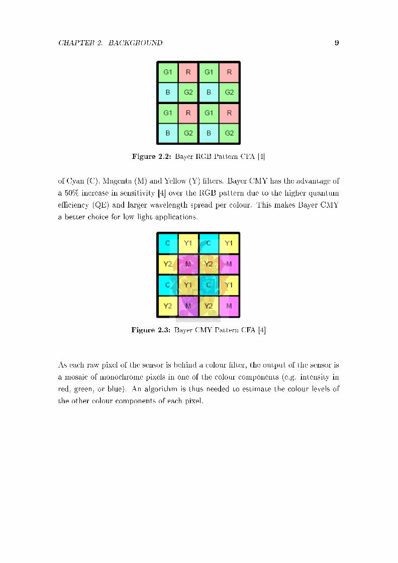
CHAPTER 2. BACKGROUND 9
Figure 2.2: Bayer RGB Pattern CFA [4]
of Cyan (C), Magenta (M) and Yellow (Y) lters. Bayer CMY has the advantage of
a 50% increase in sensitivity [4] over the RGB pattern due to the higher quantum
eciency (QE) and larger wavelength spread per colour. This makes Bayer CMY
a better choice for low light applications.
Figure 2.3: Bayer CMY Pattern CFA [4]
As each raw pixel of the sensor is behind a colour lter, the output of the sensor is
a mosaic of monochrome pixels in one of the colour components (e.g. intensity in
red, green, or blue). An algorithm is thus needed to estimate the colour levels of
the other colour components of each pixel.

CHAPTER 2. BACKGROUND 10
2.2.4 Demosaicing algorithms
A demosaicing algorithm is a mathematical process used to interpolate a complete
image from the raw matrix data received from the colour ltered image sensor.
Demosaicing is also known as CFA interpolation or colour reconstruction.
There are various demosaicing methods. Some produce better results for natural
scenes while others are preferred for printed material, which typically has a high
contrast and a limited colour palette. This shows the inherent diculty in esti-
mating the unknown pixel colours. Naturally, there is also the trade-o between
computational complexity and the quality of estimation.
The following are some demosaicing algorithms:
Quick interpolation is a low grade, nearest neighbour replication. This method
simply copies the correct colour component of an adjacent pixel. Quick inter-
polation is not computational intensive, but is unsuitable for any application
where quality is required.
Simple interpolation algorithms are uncomplicated mathematical operations
using only nearby instances of the same colour component. The simplest is
the bilinear interpolation method. In this method, the blue value of a non-
blue pixel is computed as the average of the adjacent blue pixels, and similar
for red and green. Variations of this method include bicubic-, spline- and
laplacian interpolation.
Synthetic eld based interpolation algorithms rst compute an alternate rep-
resentation from which the colour components is then interpolated. Examples
are Hue interpolation and Log hue interpolation.
Adaptive algorithms adapt its method of estimation according to character-
istics of the area surrounding the relevant pixel.
Various commercial products implement proprietary estimation methods. Very
little is freely known about these estimation techniques, but it is likely that they
incorporate similar methods as mentioned above.

CHAPTER 2. BACKGROUND 11
2.3 NAND Flash Memory
Flash memory is a non-volatile memory storage medium, which means that it does
not need power to maintain the information stored on the chip. The name, ash
memory, is derived from the organization, of the microchip, so that a section of
memory cells are erased in a single action or ash. The erasure is caused by
Fowler-Nordheim tunnel injection during which electrons pierce through a thin
dielectric material to remove an electronic charge from a oating gate associated
with each memory cell. NAND Flash devices have internal charge pumps that are
needed to generate the high voltages for writing and erasing.
2.3.1 Memory Organisation and Interface
The NAND Flash device's main memory array consists of blocks that are divided
into pages. Each page is split up into two sections: the data area and the spare
area. The spare area is typically used for housekeeping data such as checksum
values. A practical example of the memory organisation is shown in Figure 2.4.
Note that in this example a page consists of 2112 bytes, 2048 data bytes and 64
spare bytes.
NAND ash devices make use of an indirect interface. There are no dedicated
address, command, or data lines. Instead, bidirectional I/O lines combined with
some control lines are used. For example, address cycles are multiplexed onto the
I/O lines with the ALE control line high. A similar setup is used for command and
data cycles.
Higher density devices have more address cycles to access greater amount of blocks
or pages. The table in Figure 2.4 shows the format of the ve address cycles needed
to address 4224Mbits (528MB).
Using the indirect interface scheme reduces pin counts and allows for upgrades to
future densities by maintaining consistency in the system board design.

CHAPTER 2. BACKGROUND 12
Figure 2.4: Samsung K9K4G08U0M Memory Array Organisation [5]
2.3.2 Operation
2.3.2.1 Writing/Programming
NAND ash is programmed on a page-by-page basis. The programming sequence
is illustrated in Figure 2.5. Serial data loading begins by inputting the Serial Data
Input command (80h), followed by ve cycle address inputs and then the serial
page data. The Page Program Conrm command (10h) initiates the programming
process. The device now goes into a non-volatile programming period where the
loaded data is stored in the appropriate page. The R/B control line can be mon-
itored to determine when programming is complete. This delay period, tPROG, is
typically 200µs but can last up to 700µs.
The result of the internal write operation (success or failure) can be determined
by issuing the Status Register Output command (70h), reading the status and
inspecting the Write Status Bit (I/O0).

CHAPTER 2. BACKGROUND 13
Figure 2.5: Write Data & Read Status Operation [5]
2.3.2.2 Reading
The process of reading a page of data is similar to writing a page. This is illustrated
in Figure 2.6. Sequential reading of data is initiated by rst inputting the command
00h and ve address cycles followed by 30h. A waiting period follows, during which
data is transferred from the main memory array to the internal page register of the
NAND ash device. The data transfer delay, tR, is a maximum of 25µs [5]. Data
can now be read out sequentially by pulsing the read enable (RE) line.
Figure 2.6: Read Data Operation [5]
2.3.2.3 Erasing
The Erase operation is performed on a block-by-block basis and can be accom-
plished by writing the three address cycles of a specic block to the device. The
address cycles must be preceded by the Erase Setup command (60h) and followed
by the Erase Conrm command (D0h). See Figure 2.7 for a clearer explanation.
The NAND ash device will enter a busy state, tBERS, of typically 2ms to 3ms
during which the block will be erased.
According to a basic property of NAND ash devices, a write operation can only
change a stored bit from a logic 1 to a logic 0. The erase operation is thus required

CHAPTER 2. BACKGROUND 14
Figure 2.7: Block Erase Operation [5]]
to change the stored bit from a logic 0 to a logic 1. Therefore, it is critical that the
entire block in which a page resides is erased before the page can be written.
2.3.3 Bad Blocks
NAND ash memory was designed to serve as a low cost solid-state mass storage.
To obtain a bigger production yield the existence of initial bad blocks up to a
certain percentage is permissible. This lowers production costs.
Valid blocks have the same quality level and bad blocks do not aect the perfor-
mance of the valid blocks. Initial bad blocks are marked by the supplier during
extensive environmental and functional testing. The system design must mask out
the bad blocks with address mapping techniques, as the marked bad blocks' reli-
ability is not guaranteed by the manufacturer. The manufacturer guarantees that
the rst block, placed at 00h, is a valid block.
Blocks have a limited write/erase capability. Each block can be erased or repro-
grammed from 100,000 times to 1,000,000 times and therefore more bad blocks will
occur during the lifetime of the device. According to [3], the primary wear out
mechanism is believed to be excess charge trapped in the oxide of a memory cell,
and the net eect is that the erase times increase until an internal timer times out.
This error is then reported back to the system controller through the reading of
the status register.
A reference table of the bad blocks needs to be kept to insure that no bad blocks
are accessed again.

CHAPTER 2. BACKGROUND 15
2.4 Altera Nios II
2.4.1 Introduction to the Nios II
The Nios II is a soft-core embedded processor from Altera. A soft processor is a
processor created out of the congurable logic in an FPGA.
The Nios II is designed to be exible, giving the user control of a number of features
such as the cache sizes, interfaces, and execution units. In addition, hardware
support for certain operations, such as multiplication and division can be added or
removed. The congurability allows the user to trade-o features for size, in order
to achieve the necessary performance for the target application.
Programmable logic has reached such a state of advancement in terms of speed and
density that it has become an attractive alternative for implementing RISC and
CISC processors. It can form a system within which processing, peripherals, data
paths, and algorithms can be placed to create powerful, exible, and upgradeable
systems. Programmable logic is now available in forms and sizes that range from
the traditional use as glue logic up to structured ASIC replacements.
The Nios II family of 32-bit RISC embedded processors delivers more than 100
DMIPS of performance when implemented in the Cyclone II FPGA family. Since
the processors are soft-core and exible, it is possible to choose from a nearly
unlimited combination of system congurations thereby enabling the processor to
meet the requirements with regard to features, level of performance and cost.
The Nios II processor family consists of three cores, fast (Nios II/f), standard
(Nios II/s) and economy (Nios II/e), each optimized for a specic price and per-
formance range. All three cores share a common 32-bit instruction set architecture
and are 100 percent binary code compatible. A library of commonly used periph-
erals and interfaces is included in the Nios II development kit. A complete list
of SOPC builder-ready Intellectual Property (IP) and peripherals can be found at
the Altera Web page. The interface-to-user-logic wizard in the SOPC Builder soft-
ware enables the creation of custom peripherals and their integration into Nios II
processor systems.
CHAPTER 2. BACKGROUND 16
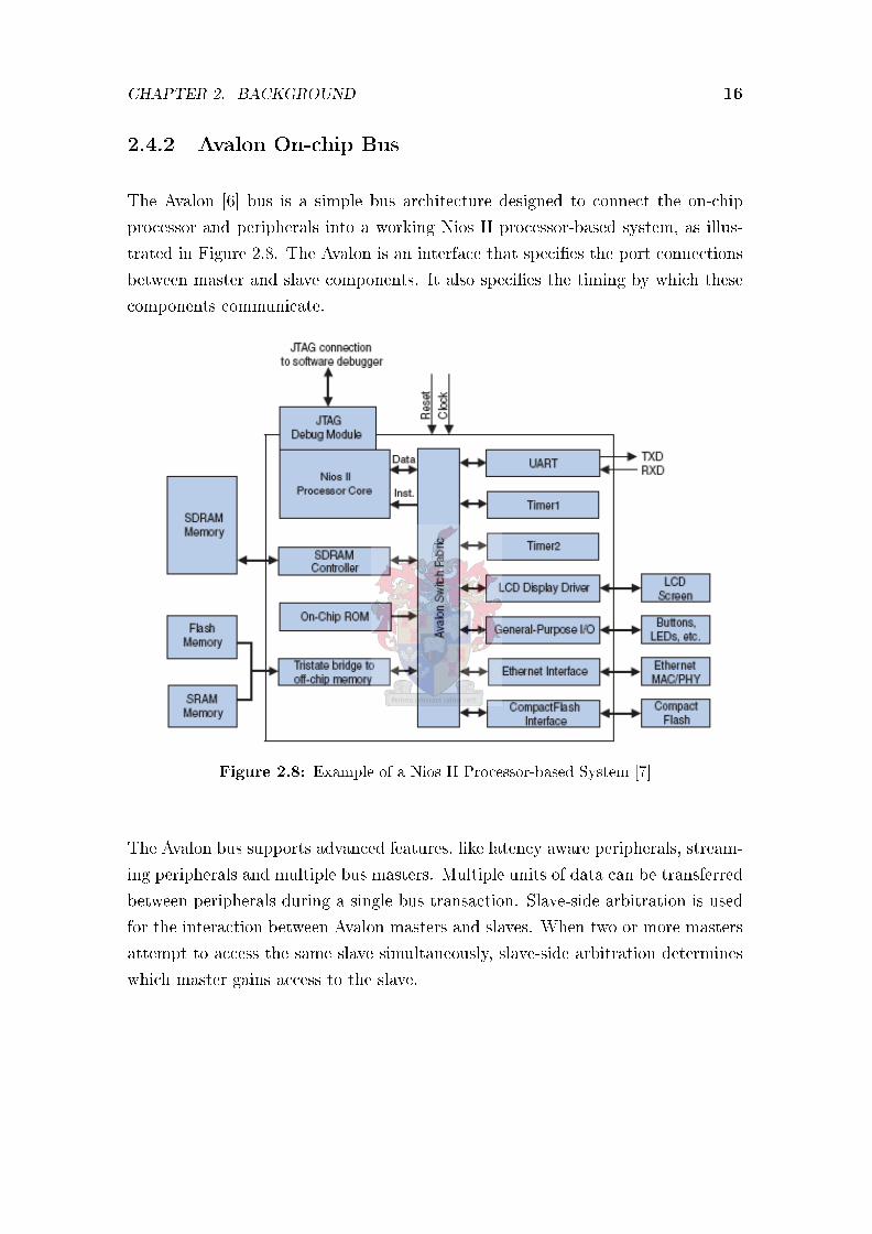
2.4.2 Avalon On-chip Bus
The Avalon [6] bus is a simple bus architecture designed to connect the on-chip
processor and peripherals into a working Nios II processor-based system, as illus-
trated in Figure 2.8. The Avalon is an interface that species the port connections
between master and slave components. It also species the timing by which these
components communicate.
Figure 2.8: Example of a Nios II Processor-based System [7]
The Avalon bus supports advanced features, like latency aware peripherals, stream-
ing peripherals and multiple bus masters. Multiple units of data can be transferred
between peripherals during a single bus transaction. Slave-side arbitration is used
for the interaction between Avalon masters and slaves. When two or more masters
attempt to access the same slave simultaneously, slave-side arbitration determines
which master gains access to the slave.

CHAPTER 2. BACKGROUND 17
The Nios II's instruction and data buses are both implemented as Avalon master
ports. The data master port connects to both the peripheral and the memory
components, while the instruction master port only connects to the memory com-
ponents.
2.4.3 Development Tools
A complete set of tools are available for the hardware design, including Quartus II
design software, the SOPC Builder system development tool, ModelSim-Altera soft-
ware, and SignalTap II embedded logic analyzer.
The SOPC Builder system development tool is used for creating, conguring and
generating a hardware Nios II processor-based system. Launching from within the
Quartus II design software, SOPC Builder provides an intuitive, wizard-driven,
graphical user interface for creating, conguring, and generating system-on-a-pro-
grammable-chip (SOPC) designs.
To make the software design ow as easy as possible, it is possible to accomplish all
software development tasks including editing, building, debugging programs, and
ash programming within the Nios II IDE.
To develop and debug a Nios II processor-based system a PC, an Altera FPGA de-
vice and a JTAG download cable is required. The Nios II architecture supports a
JTAG debug module that provides on-chip emulation features, enabling the proces-
sor to be controlled from a remote host PC. The Nios II IDE can communicate with
the JTAG module on the Nios II processor-based system. This allows downloading
of programs to memory, starting and stopping program execution, setting break-
points and watch points, analysing registers and memory, and collecting real-time
execution data.

CHAPTER 2. BACKGROUND 18
2.5 Communication Methods
2.5.1 I2C
I2C [4][8] is a two-wire serial bus and was originally developed by Philips. I2C does
not need a chip select or arbitration logic, making it cheap and simple to implement
in hardware.
The two I2C signals are serial data (SDA) and serial clock (SCL). Together, these
signals make it possible to support serial transmission of 8-bit bytes of data over
the two-wire serial bus. The device that initiates a transaction on the I2C bus is
termed the master (Not to be confused with the Avalon master and slave). The
master normally controls the clock signal. The data on the SDA line is valid when
the master switches the SCL line from high to low. A device being addressed by
the master is called a slave.
If an I2C slave is slower than the master it can hold o the master in the middle of
a transaction using clock stretching. Clock stretching is when the slave keeps SCL
low until it is ready to continue. Most I2C slave devices do not use this feature,
but every master supports it.
The I2C protocol supports multiple masters, but most system designs include only
one. There may be one or more slaves on the bus. Both masters and slaves can
receive and transmit data bytes.
Each I2C-compatible hardware slave device comes with a predened device address.
The master transmits the device address of the intended slave at the beginning of
every transaction. Each slave is responsible for monitoring the bus and responding
only to its own address. This addressing scheme limits the number of identical
slave devices that can exist without contention on an I2C bus.
The master begins the communication by issuing the start condition [9]. The master
continues by sending a unique 7-bit slave device address, with the most signicant
bit (MSB) rst. The eighth bit after the start, the Read/Write, species whether
the slave is now to receive (0) or to transmit (1). This is followed by an ACK bit

CHAPTER 2. BACKGROUND 19
issued by the receivers, acknowledging receipt of the previous byte. The transmitter
(slave or master, as indicated by the bit) then transmits a byte of data starting with
the MSB. At the end of the byte, the receiver (whether master or slave) issues a
new ACK bit. This 9-bit pattern is repeated if more bytes need to be transmitted.
A write transaction is when the slave is receiving. When the master is done trans-
mitting all of the data bytes it wants to send to the slave, it monitors the last
ACK and then issues the stop condition. In a read transaction where the slave is
transmitting, the master does not acknowledge the nal byte it receives. This tells
the slave that its transmission is done. The master then issues the stop condition.
2.5.2 LVDS
Low voltage dierential signalling [10], or LVDS, is an electrical signalling system
that can run at very high speeds over cheap, twisted-pair copper cables. It was
introduced in 1994 and its use has since become popular in very high-speed networks
and computer buses.
LVDS uses the dierence in voltage between two wires to signal information. De-
pending on the logic level to be sent, the transmitter sends a small current, nomi-
nally 3.5mA, into one of the wires. The current passes through a resistor, matched
to the characteristic impedance of the cable at the receiving end, approximately
100Ω to 120Ω, and then returns in the opposite direction along the other wire. The
voltage dierence across the resistor is therefore about 350mV. The receiver senses
the polarity of this voltage to determine the logic level.
The small amplitude of the signal and the tight electric- and magnetic-eld coupling
between the two wires reduces the amount of radiated electromagnetic noise.
The low common-mode voltage (the average of the voltages on the two wires) of
about 1.25V allows LVDS to be used with a wide range of integrated circuits with
power supply voltages down to 2.5V or lower. The low dierential voltage, about
350mV as stated above, causes LVDS to consume very little power compared to
other systems. For example, the static power dissipation in the LVDS load resistor

CHAPTER 2. BACKGROUND 20
is 1.2mW, compared to the 90mW [11] dissipated by the load resistor for an RS-422
signal. This power eciency is maintained at high frequencies because of the low
voltage swing.
LVDS is often used for serial data transmission, which involves sending data bit-
by-bit down a single wire, as opposed to parallel transmission, during which several
bits, usually in multiples of eight, are sent down many wires at once. Its high speed
(a maximum data rate of 655 Mbit/s over twisted-pair copper wire) and its use of
in-channel synchronisation, makes it possible to send serial data faster than could
be done with a parallel bus.
When serial data transmission is not fast enough, data can be transmitted in parallel
using an LVDS pair for each bit. This system is called bus LVDS, or BLVDS, and
uses a higher driving current of 10mA, instead of 3.5mA.
2.5.3 CAN Bus
Controller Area Network (CAN) [10] is a multicast, shared, serial bus standard,
originally developed in the 1980's by Robert Bosch GmbH. CAN was specically
designed to be robust in electromagnetically noisy environments and utilizes a dif-
ferential bus with special transceivers to support bit-wise arbitration. It can be
even more robust against noise if twisted pair wire is used. CAN was initially cre-
ated for automotive purposes as a vehicle bus, but is today used in a variety of
embedded control applications.
Bit rates up to 1Mbit/s are possible at networks length below 40m. Decreasing the
bit rate allows longer network distances (e.g. 125kbit/s at 500m).
CAN transmits data through a binary model of dominant bits and recessive
bits, where a dominant bit is a logical 0 and a recessive bit is a logical 1. If
one node transmits a dominant bit and another node transmits a recessive bit, the
dominant bit wins. This is similar to a logical AND between the two as illustrated
in Table 2.1.

CHAPTER 2. BACKGROUND 21
Table 2.1: Bus state with two nodes transmitting simultaneously
dominant (0) recessive (1)dominant (0) dominant (0) dominant (0)recessive (1) dominant (0) recessive (1)
As an example, if node-A is transmitting a recessive bit, and node-B sends a dom-
inant bit, node-A will see a dominant bit, and recognise that a collision occurred.
Node-B will continue sending bits, while node-A will stop. All other collisions are
invisible, as the same data will be transmitted on the bus. A dominant bit is as-
serted by creating a voltage across the wires, while a recessive bit is simply not
asserted on the bus. If any node sets a voltage dierence, all nodes sees it, and
hence a dominant bit is transmitted.
When two or more devices start transmitting at the same time, there is a priority
based arbitration scheme to decide which device will be granted permission to con-
tinue transmitting. Commonly a Carrier Sense Multiple Access/Bitwise Arbitration
(CSMA/BA) scheme is implemented.
During arbitration, each transmitting node monitors the bus state and compares
the received bit with its own transmitted bit. If a dominant bit is received, while
a recessive bit is transmitted, the node loses arbitration and stops transmitting.
Arbitration is performed during the transmission of the identier eld (ID). The
ID with the lowest numerical value has the highest priority. Each node starting to
transmit at the same time sends an ID starting from the MSB bit. As soon as a
node's ID is a larger number (lower priority) it will be sending a 1 (recessive bit)
and see a 0 (dominant bit), thus the node will stop transmitting. At the end of
ID transmission, all nodes, but one has stopped transmitting, allowing the highest
priority message to pass through unobstructed.
Chapter 3
Design Specications
A Kodak KAC-1310 Image Sensor was supplied to be integrated into a camera
system aimed to be used on a nanosatellite. No strict specications were given as
the nanosatellite was only in the concept phase. It was however desired that the
camera should be able to take images of at least 1024 × 1024 pixels and that it
should be capable of storing at least 100 of these images in non-volatile memory.
The LVDS standard was recommended for the fast data down link, while CAN bus
was optional for control of the camera system. The requirements also suggested
the use of a soft-core processor in the design for control and possible real time
interpolation of the images. Furthermore, the camera system must also be able to
operate from a 5-12V power bus. The optics part of the application is not covered
in this thesis. Only an image acquiring and storing device is required.
22

CHAPTER 3. DESIGN SPECIFICATIONS 23
3.1 Design Constraints
3.1.1 Timing and Data Rate Calculations
3.1.1.1 CMOS Sensor Calculations
The CMOS Sensor is capable of taking images in two modes, either Continuous
Frame Rolling Shutter capture mode (CFRS) for video capture or Single Frame
Rolling Shutter capture mode (SFRS) for still images. As the camera system will
take still images only, the timings and data rate calculations for SFRS alone will
be considered.
In SFRS mode, the total time to capture a frame is divided into two parts, the pixel
integration time and the readout time. See Figure 3.1. The pixel integration time,
also known as electronic exposure timing in photographic terms, can be widely
varied from a small fraction of the frame readout time to the entire frame time.
This electronic exposure time can be set by the user and will not inuence the data
rate calculations.
Figure 3.1: Single Frame Capture Mode (SFRS) [4]
The image dimensions can be sized by setting the Window of Interest (WOI) reg-
isters, WOI Row Depth (wrd) and WOI Column Depth (wcd). The image can also

CHAPTER 3. DESIGN SPECIFICATIONS 24
be padded with blanking pixels (invalid dark pixels) to slow down readout times
by increasing the Virtual Frame (VF) Column Width (vcw). The readout time can
be calculated using:
Readout T ime = Trow × (wrd + 1) (3.1.1)
where
Row Time (Trow) = (vcw + shA + shB + 19µs)×MCLKperiod (3.1.2)
Table 3.1 gives a summary of readout times at dierent MCLK frequencies for a
1280×1024 pixel image. The Sample and Hold times, shA and shB, is kept at their
default values of 10µs.
Table 3.1: Readout Times compared to MCLK
MCLK [MHz] Row Time [µs] Readout Time [s]1.00 1319.000 1.3511.25 1055.200 1.0811.50 879.333 0.9001.75 753.714 0.7722.00 659.500 0.6752.25 586.222 0.6002.50 527.600 0.5402.75 479.636 0.4913.00 439.667 0.4504.00 329.750 0.3385.00 263.800 0.27010.00 131.900 0.13515.00 87.933 0.09020.00 65.950 0.068
The maximum data rate occurs during the Horizontal Clock (HCLK) bursts, Fig-
ure 3.1, where a pixel is readout on every rising edge of the HCLK. In each burst,
one row of pixel data is clocked out. The HCLK is a delayed MCLK and thus the
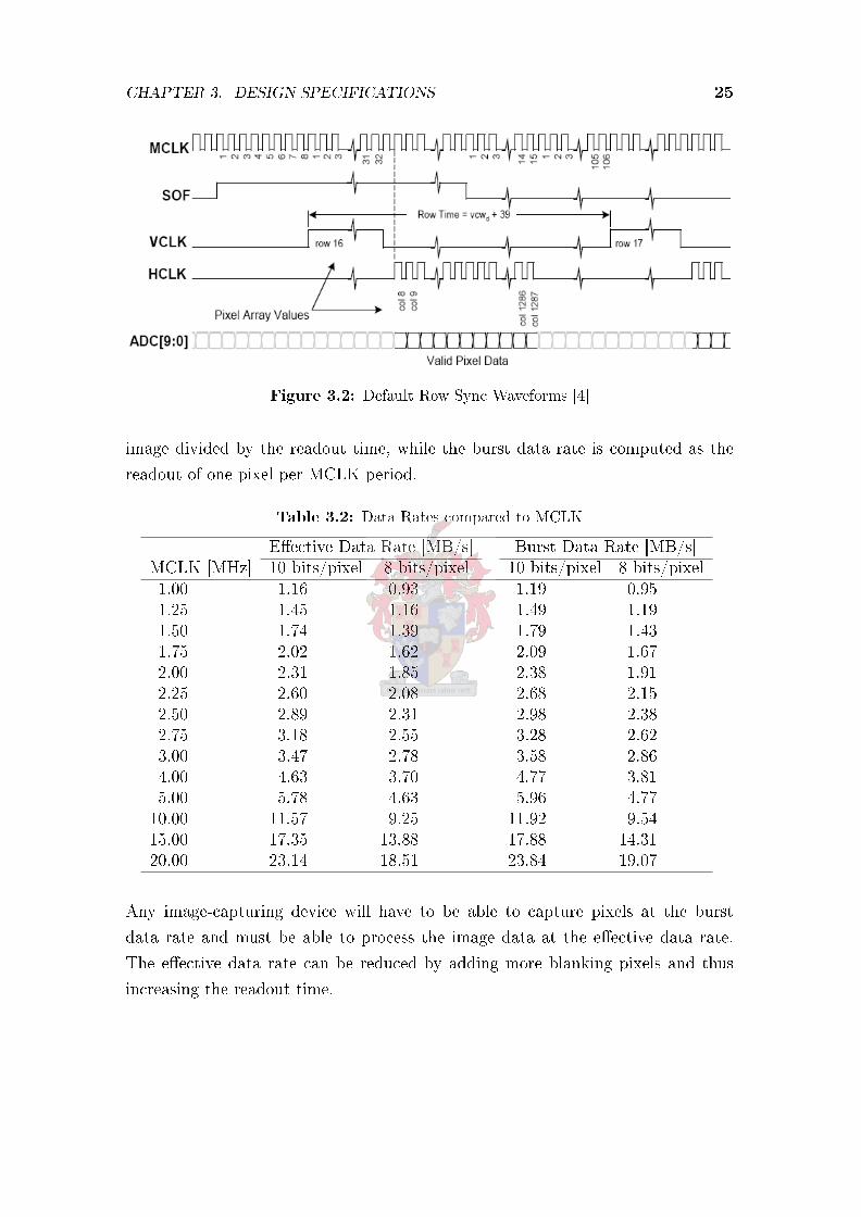
pixel rate is proportional to the MCLK frequency, Figure 3.2.
In Table 3.2 the eective data rate and the burst data rate for 10 and 8 bits/pixel
is shown for dierent MCLK frequencies. The eective data rate is the size of an
CHAPTER 3. DESIGN SPECIFICATIONS 25
Figure 3.2: Default Row Sync Waveforms [4]
image divided by the readout time, while the burst data rate is computed as the
readout of one pixel per MCLK period.
Table 3.2: Data Rates compared to MCLK
Eective Data Rate [MB/s] Burst Data Rate [MB/s]MCLK [MHz] 10 bits/pixel 8 bits/pixel 10 bits/pixel 8 bits/pixel1.00 1.16 0.93 1.19 0.951.25 1.45 1.16 1.49 1.191.50 1.74 1.39 1.79 1.431.75 2.02 1.62 2.09 1.672.00 2.31 1.85 2.38 1.912.25 2.60 2.08 2.68 2.152.50 2.89 2.31 2.98 2.382.75 3.18 2.55 3.28 2.623.00 3.47 2.78 3.58 2.864.00 4.63 3.70 4.77 3.815.00 5.78 4.63 5.96 4.7710.00 11.57 9.25 11.92 9.5415.00 17.35 13.88 17.88 14.3120.00 23.14 18.51 23.84 19.07
Any image-capturing device will have to be able to capture pixels at the burst
data rate and must be able to process the image data at the eective data rate.
The eective data rate can be reduced by adding more blanking pixels and thus
increasing the readout time.

CHAPTER 3. DESIGN SPECIFICATIONS 26
3.1.1.2 NAND Flash Data Rate Calculations
Writing large amounts of data to NAND ash memory can take longer than ex-
pected, as a write operation to NAND ash is always followed by a time delay.
This delay can last up to 700µs [5] and only after this delay can a next page be
written to the device. The reason for this delay is that the device goes into a busy
state where the device transfers the data from its cache register to the ash cells.
See Figure 3.3.
The sequence to write a page of data to a NAND ash device is as follows:
1. Write 6 setup cycles,
2. Wait ALE signal to Data Loading time delay, tADL, 100ns,
3. Write 2112 bytes of data (2048 data + 64 spare bytes),
4. Write 1 program command cycle,
5. Wait tPROG, which can last up to 700µs,
6. If desired check if write was successful.
A write cycle, tWC , to write one byte, can be no shorter than 30ns [5]. Therefore,
one page (2112 bytes) can be written at a maximum burst data rate of 31.79MB/s.
Writing one page takes 30ns×2112 = 63.36µs. Adding tPROG, tADL and 7 setup cy-
cles to this time gives 763.67µs needed to write one page and results in a continuous
data rate of 2.64MB/s.
This means that although the NAND ash device can handle high data rates in
excess of 30MB/s for data blocks less than a page size, it can only handle a con-
tinuous data rate of 2.64MB/s if multiple pages has to be stored. If needed this
data rate can be increased by using multiple NAND ash devices in a round-robin
fashion as described in [3].
Table 3.3 shows the burst and continuous data rates compared to dierent write
cycles, tWC , that is capable when using a single NAND ash device.

CHAPTER 3. DESIGN SPECIFICATIONS 27
Figure 3.3: NAND ash page write sequence [5]
Table 3.3: NAND Flash Burst and Continuous Write Data Rates
tWC [ns] Write time/page [us] Burst write [MB/s] Continuous write [MB/s]30 763.670 31.79 2.63731 765.789 30.76 2.63032 767.908 29.80 2.62333 770.027 28.90 2.61634 772.146 28.05 2.60935 774.265 27.25 2.60136 776.384 26.49 2.59437 778.503 25.77 2.58738 780.622 25.10 2.58039 782.741 24.45 2.57340 784.860 23.84 2.56645 795.455 21.19 2.53250 806.050 19.07 2.499
3.1.2 Memory Capacity
The minimum capacity of the NAND ash memory depends on the size and the
amount of images that needs to be stored. It is required that a minimum of a
100 images need to be stored, as images can only be downloaded to the ground

CHAPTER 3. DESIGN SPECIFICATIONS 28
station when the satellite is in range. Images must also have a resolution of at least
1024x1024 pixels.
Assuming 10 bits/pixel, the standard output of the KAC-1310 CMOS image sensor,
the size of one image is 1.25MB/image. In order to store 100 images the NAND
ash device's memory capacity must exceed 125MB.
The preceding calculation was done for raw images - no demosaicing. If interpo-
lation is considered, then 3 bytes/pixel is necessary, assuming that a 24bit/pixel
interpolation scheme is used. These images are 3 times larger in memory size and
thus the total storage size needed is 3 × 125MB = 375MB.
This is the minimum memory size, as no bad blocks in the NAND ash device
is taken into account in this calculation. The failure of NAND ash blocks will
occur more rapidly in space than on earth because of radiation (Section 3.1.5).
Therefore, when choosing the capacity of the NAND ash memory, extra memory
must be allowed for bad blocks.
3.1.3 Power Constraints
Satellites are powered by both rechargeable batteries and solar panels. A nanosatel-
lite's dimensions are much smaller than that of a larger satellite. Smaller dimensions
infer less area for solar panels and thus less power is generated for the satellite to
operate from. Therefore, any component used on the nanosatellite must use power
conservatively. This is one of the main design considerations for the camera system.
Preliminary calculations show that the peak power use of the camera system will
be more than 350mW as:
PowerKAC−1310 @13.5MHz = 250mW
and
PowerSamsung K9K4G08U0M = 30mA× 3.3V = 99mW

CHAPTER 3. DESIGN SPECIFICATIONS 29
A design with a peak power usage preferably less than 1W will be attempted for
this thesis.
3.1.4 Physical Size and Mass Constraints
As mentioned before, a nanosatellite has small dimensions and thus onboard com-
ponents must adhere to this constraint.
Component mass must be kept to a minimum, because the cost of launching a
satellite is directly proportional to its mass. The design should therefore attempt
to keep the camera's size and mass to the absolute minimum.
3.1.5 Radiation
This camera's application is for use onboard a satellite and will therefore be sub-
jected to space radiation. Fortunately, the radiation of the camera's circuitry will
be reduced by the 2 - 3mm thick aluminium panels of the satellite's body.
Radiation of the CMOS sensor is of a bigger concern as it is not shielded by the
aluminium panels. The CMOS sensor is only covered by the optical lens system,
which does not provide protection from radiation. The biggest source of space
radiation for LEO satellites is the sun [1]. As the camera will not be used to image
the sun, but more likely the earth, the lens system, and therefore the CMOS sensor,
will mostly face the earth. The earth does not produce radiation and therefore the
CMOS sensor will not be subjected to excessive radiation.
Studies done in the ESL on the radiation tolerance of NAND ash memory has
concluded that NAND ash memory should be capable of handling the radiation
experienced in LEO for at least 5 years.
This thesis will not test the design for radiation hardness, but will assume that the
satellite body and orientation will shield the system from radiation.
CHAPTER 3. DESIGN SPECIFICATIONS 30
3.1.6 Bad Block Table
Any decent design that makes use of NAND ash memory must keep record of the
bad blocks in the NAND ash device. This can be done by storing the information
in a lookup table. The bad block lookup table must be saved in a non-volatile
memory space so that the information will not be lost when power is removed. A
good place to store the bad block table would be in a known good block of the
NAND ash device.
The bad block table is dynamic as new bad blocks can form during the lifetime of
the device. The data structure of the bad block table must be suitable for random
bad block address changes and lookups must be relatively ecient. To allow for
random access the bad block table might be loaded into the memory of a controller
and should therefore be small as not to waste valuable resources.
3.1.7 Error Correcting Codes
Radiation and device degrading can cause bit ips in stored data. This corrupted
data can to some degree be corrected by using error correcting codes (ECC). Various
ECC codes exist, but a fundamental property of these codes is the need for extra
memory to store the computed codes. A very well known ECC is the Hamming
code. All these ECC codes are based on some form of parity bit scheme and are
limited to the extend of their correction capabilities.
For this design some controller that is capable of handling the required data rates,
while still processing the ECC codes, is needed. Extra storage memory will also be
necessary to store the nal ECC.
3.1.8 Optics
A camera system needs an optical element to focus the real image on the light
sensitive image-capturing instrument, like the CMOS image sensor.

CHAPTER 3. DESIGN SPECIFICATIONS 31
The design of optical lenses is a eld of study in its own right and is very application
specic. As the exact use onboard the satellite or application of this camera system
is not yet known it was decided not to focus on the design of a lens system, but
rather on the capturing and storing of the image data from the CMOS image sensor.
3.1.9 Complexity and Reliability
The risk in making satellites is quite high and therefore the satellite and all subsys-
tems must be extremely reliable. It is dicult to debug and x a system in space.
Systems must therefore be capable of either correcting themselves, or be able to
work with reduced functionality.
By keeping the design both simple and modular, future upgrades and maintenance
is easier. Modular systems can be tested individually and faults localised more
easily.
3.1.10 Cost
As with any engineering project, cost must be kept to a minimum and this project is
no exception. The project is sponsored mainly by SunSpace1 and other commercial
companies.
The project did not have unlimited resources, and therefore decisions made regard-
ing component selection, choices between dierent development software, and the
number of PCB layers were all made keeping costs at a minimum.
1SunSpace was established in 2000, through the Unistel Group and the Oce of Intellectual
Property of the University of Stellenbosch.

Chapter 4
System Design Overview
The design requires the use of a FPGA. FPGAs are very versatile and if designed
well the whole design can be very compact. The design will only consist of the
CMOS image sensor, the NAND ash memory, a FPGA and the required power
system.
All the glue logic for the interfaces to the CMOS image sensor and NAND ash
memory can be implemented in the FPGA. It is possible to implement all the
communication drivers in the FPGA along with a soft processor to do the house-
keeping work. The necessity for extra external memory can be avoided by choosing
the correct FPGA with enough internal RAM.
4.1 FPGA Considerations
Since the main system design is implemented in a FPGA, selecting the correct fam-
ily of FPGA is of vital importance, especially when designing high-speed devices. If
the design grows to exceed the selected device there must be a device in the family
that is larger in capacity to migrate to.
Various FPGA vendors were considered but nally it was decided to use the Altera
Cyclone II family. The reasons for this choice will be discussed next:
32

CHAPTER 4. SYSTEM DESIGN OVERVIEW 33
Intellectual Properties (IP) - The Altera FPGAs supports mega functions
which include FIFOs, memory structures, LVDS drivers, JTAG UARTs, but
most importantly the Nios II soft-core processor. The Nios II is also very well
supported and documented.
Internal RAM - The Altera Cyclone II families oer the highest amount of
internal RAM per device. Abundant internal RAM is needed, as no external
RAM will be used.
Power usage - The Cyclone II uses half the power than the Cyclone I and
comparable Xilinx devices.
Migration - The Cyclone II oers good migrating possibilities.
Speed - Initial simulation with the Cyclone II proved that the Cyclone II
family is capable of the high internal clock speeds necessary for this design.
Availability - The Cyclone II has been on the market for a reasonable amount
of time and is readily available.
Development Software - The University of Stellenbosch has full licenses for
the Altera's development software and the author is fairly familiar with these
development tools.
Capacity - The Cyclone II devices oer a high capacity of logic elements in
standard packages.
The Altera Cyclone II EP2C35F484C6 FPGA was selected to be utilised in the
design. Although SRAM based FPGA are not widely used in space applications
due to radiation upsets, the selection is still viable, as the radiation upsets will
not degrade the reliability of the satellite. The camera system is not a vital life
component of the satellite and if an upset should occur the camera can simply be
reset and recongured by the OBC.
The Cyclone II EP2C35F484C6 contains four phase lock loops (PLL) and hardware
multipliers. It is capable of parity bit checking on internal memory and can do
Cyclic Redundancy Checks (CRC) [12] on the FPGA's conguration. All these
features make the Cyclone II a very appealing choice.

CHAPTER 4. SYSTEM DESIGN OVERVIEW 34
4.2 VHDL Design Overview
The following discussion will explain the system's VHDL design as seen in the grey
area of Figure 4.1.
Figure 4.1: System Block Diagram
4.2.1 Data Widths
The CMOS image sensor outputs the pixel data in a 10-bit wide bus. The NAND
ash device has an 8 bit I/O bus. Packing 10 bits into 8-bit packets can become
a strenuous task and may cause that one image worth of data does not t per-
fectly into a NAND block partition or even worse, a page partition. The result
of this is that one partition can contain the data of two images. This makes data
management more complex.
To reduce this complexity and future debugging eorts it was decided to keep the
design simple and choose the data width as 8 bits. The eect of this decision is
that the two least signicant bits from the CMOS image sensor output is discarded
and therefore the image colour depth is reduced. An advantage of this choice is
that the required data rates can be relaxed.

CHAPTER 4. SYSTEM DESIGN OVERVIEW 35
4.2.2 Data Routing
One of the main challenges of this design is transferring data from the CMOS image
sensor to the NAND ash memory device, while simultaneously downloading images
from the NAND ash memory.
It was decided to use two FIFOs to shift the data around. One FIFO is used to
transfer data to the NAND ash memory and the other FIFO to transfer data from
the NAND ash memory. Each FIFO will use a dual-clock system, meaning that
there are two separate clocks for reading from and writing to each individual FIFO.
See Figure 4.2.
Figure 4.2: Dual Clock FIFO
By using two clocks, it is possible to input data into the FIFO at one particular
data rate while concurrently outputting data from the FIFO at a dierent data
rate. This attribute is very useful as image data can now be buered in the FIFO
and at a specied time be ushed out at a much higher data rate to the NAND
ash memory.
Writing data as fast as possible to the NAND ash reduces the average power of the
system, as the NAND ash device will only be operational for very short intervals.
The NAND ash device consumes 99mW during a write or read operation but only

CHAPTER 4. SYSTEM DESIGN OVERVIEW 36
66µW during idle time. It thus makes sense to reduce the operational time of the
NAND ash device.
Similarly, the FIFO used to read the data from the NAND ash memory could be
used to buer the high-speed data from the NAND ash device and then output
the data at a slower rate for external devices.
A FIFO features optional signals such as asynchronous clear, empty-, full- and half-
full signals. The asynchronous clear will be used to clear the FIFO on reset, while
the empty and full signals will be used to determine the status of the FIFOs. The
half-full signal warns that the FIFO is half-full and will be used to signal that the
buered data is ready to be shifted to the next module.
Having this feature, it was decided to make the FIFO's depth twice that of a NAND
ash page size. Thus 2×2048 bytes = 4096 bytes. This allows the system to buer
a full page worth of data before writing it to NAND ash memory. The deeper
Input-FIFO permits more than one page to be buered for when the NAND ash
memory is busy outputting read data into the Output-FIFO.
Seamless concurrent reading and writing to the mass NAND ash memory can be
implemented using this feature.
4.2.3 Error Detecting and Correcting
To make the mass memory more robust against radiation and random bit ips,
some form of error correcting code (ECC) needs to be implemented in an error
detecting and correcting (EDAC) scheme. NAND ash suppliers recommends using
Hamming code ECC to recover the error [13].
The recommended Hamming code algorithm computes 24 bits (3 bytes) for every
512 bytes of data. Thus to protect a full page of 2048 bytes, 12 bytes needs to be
added [14]. Fortunately, NAND ash comes with a spare area in each page where
these codes can be stored. This Hamming code can correct a single bit ip error
in each protected sector and detect if there is more than one error. Since the page

CHAPTER 4. SYSTEM DESIGN OVERVIEW 37
is divided into four sectors, 4× 512 bytes, four ipped bits can be corrected in the
page if they all occur in separate sectors.
When a page is written to the ash memory 12 ECC bytes are computed and
appended to the stored data. When the same stored page is read from ash mem-
ory, the same algorithm is used to compute another 12-byte code word. The two
code words are then compared and any errors are detected. If possible, they are
corrected.
To implement this EDAC system a code word generator, a code word comparator,
FIFO and an error correction unit is necessary. The FIFO is needed to temporarily
store the read page while the second 12-byte code word is generated and compared
with the stored code word. This requirement works well with the data router FIFO
design in section 4.2.2. Figure 4.3 illustrates the data router FIFOs combined with
the EDAC system.
Figure 4.3: Data Router with EDAC Block Diagram
4.2.4 NAND Flash Interface Module
The NAND Flash Interface module is implemented as a number of state machines
used to setup the correct command and address cycles for interfacing with the
NAND ash device. For each operation, i.e. writing, reading, erasing, or resetting,
there is a separate state machine. Each state machine controls the exact sequence

CHAPTER 4. SYSTEM DESIGN OVERVIEW 38
of commands and addresses for its operation since the number of command and
address cycles diers for each command.
Figure 4.4: NAND Flash Memory Interface Block Diagram
All the state machines need access to the control and data lines of the NAND ash
device and therefore a multiplexer will be implemented to connect the appropriate
state machine to these lines. A controller that receives commands from the outside
selects the appropriate state machine to execute the desired operation, while also
controlling the multiplexer.
4.2.5 Bad Block Table
The bad block table needs to be stored in non-volatile memory to preserve the data
during power cycling. As the camera system will be using NAND ash memory to
store non-volatile data, it is logical to store the bad block table in the NAND ash
device itself. The NAND ash manufacturer guarantees that the rst block of the
device is a valid block and that it is capable of 1000 program/erase cycles without
the need for error checking. The bad block table will therefore be stored in the rst
block of the NAND ash device.

CHAPTER 4. SYSTEM DESIGN OVERVIEW 39
The negative eect of storing the bad block table in the ash memory is the com-
plexity in accessing and updating the table dynamically. The bad block table will
therefore have to be loaded into external RAM at start up and again be stored at
the end of the camera's operation. The design is implemented in a FPGA where
RAM is predominantly limited. The bad block table's memory footprint must
consequently be as small as possible.
Lookups and changes to the table must be ecient and should not require intensive
computation.
The method of keeping track of bad blocks used in [3] is unnecessarily complicated,
as it uses excess memory and is hard limited to the amount of bad blocks it can
keep track of. It also requires the table to be sorted periodically.
A much simpler and elegant solution is to represent the status of each block in the
NAND device as a single bit. Structuring the table in an 8 × 512 bit matrix not
only saves memory but sorting is redundant. Using this scheme the status of every
block is represented as valid or invalid. Any block's 12 bit address can now simply
be mapped and compared to the valid bit in the bad block table. See Figure 4.5.
Figure 4.5: An Example of the proposed Bad Block Table organisation
This solution keeps track of all 4096 blocks in only 512 bytes, eectively four times
less memory than the proposed method in [3]. The table's size is also smaller than
a NAND ash device's page size and thus only one access to ash memory is needed
to load or store the bad block table.

CHAPTER 4. SYSTEM DESIGN OVERVIEW 40
4.2.6 Image Storage Structure
The specication for the camera system requires that at least 100 images must be
stored in NAND ash memory. Before a decision can be made about a structure
to store these images in, some insight is needed:
A non-interpolated image is 1.25MB in size and will span 10 blocks of NAND ash
memory:1.25MB
2048 bytes/page× 64 pages/block= 10 blocks
An interpolated images is 3 times 1.25MB (Section 3.1.2) and will thus span 30
blocks of ash memory.
Bad blocks can also develop during the lifetime of the system and will cause the
memory space to become fragmented. Dividing the memory space into predened
image partitions will therefore not work. Keeping a le system is also to complex
and dicult to maintain. A memory structure that is simple to implement and
easily organised is desired.
It was decided to use the ash memory space as a linear list of blocks. The bad
block table will map out all bad block addresses allowing the memory space to
appear continuous. Images will be stored consecutively in ash from block 1 to
block 4095, skipping bad blocks, until the ash memory is full. Images will be
downloaded from block 1 and a pointer will be kept to the last block and page
that has been downloaded. A second pointer will be kept to indicate the next open
block to where image data can be written.
Erasing individual blocks are not allowed, as this will leave the continuous memory
space fragmented and dicult to manage. Instead, the memory blocks can only be
erased all at once as a unit.
This method also implements some form of wear levelling as all the blocks in the
device are likely to be programmed and erased equally often.

CHAPTER 4. SYSTEM DESIGN OVERVIEW 41
4.2.7 Bad Block Table & Address Manager Module
Valid addresses needs to be generated from the bad block table (BBT) on access
requests to the NAND ash device. The data router, bad block table and storage
structure must also operate in unison. This module will full this function.
The address manager creates incremental addresses starting at block 1. The gener-
ated address is compared to the block address, read from the bad block table, and
is skipped if it is marked as a bad block.
Figure 4.6: Bad Block Table & Address Manager Block Diagram
When a request is received to write a page to ash memory the last written block
address is passed to the block address generator. The block address generator
compares the address to the bad block table (Section 4.2.5) and if it is found to be
a bad block the address generator will increment the block address. This sequence
will be repeated until a valid block is found, after which the initiating process will
be signalled that a valid block address is available and that writing or reading may
commence. This ensures that only valid blocks are accessed.
The module will handle the following low-level requests:
Load BBT - multiplexes the output of the Output-FIFO to the BBT memory,
and sends a command to the NAND Interface module to read the rst page
of block 0.

CHAPTER 4. SYSTEM DESIGN OVERVIEW 42
Store BBT - multiplexes the output of the BBT memory to the Input-FIFO.
Block 0 is erased before the write page command is send to the NAND Inter-
face module.
Erase all - starts erasing all the image data blocks, starting at block 1 and
ending at block 4095.
Write page - requests a valid block and page address from the block address
generator and then writes the buered image from the Input-FIFO to the
NAND ash memory.
Read page - requests a valid block and page address from the block address
generator starting from the last downloaded address. The NAND Interface
module is then commanded to read a page from NAND ash memory at the
generated address. The read data is then buered in the Output-FIFO.
Reset ash - implemented for possible future use.
The Data Router with EDAC, NAND Interface Module and the Bad Block Table
& Address Manager Module will, from here on, collectively be known as the Image
Exporter.
4.2.8 Embedded System Controller
The whole design needs to be controlled and must be able to communicate with
the OBC. It was decided to use the Altera Nios II soft-core processor for this
purpose. Using a processor enables changes to the system to be easily made in
software. Dierent interpolation algorithms can simply be written in a high level
programming language such as ANSI C. Many communication drivers are available
to interface directly with the Nios II system via the Avalon bus and changing to a
dierent protocol is as simple as adding the new soft-core module. Software drivers
exist for these modules and will have to be loaded.
The Nios II is very easy to use and debugging is facilitated by using the JTAG
UART. No extra hardware is required to use this feature as the standard JTAG

CHAPTER 4. SYSTEM DESIGN OVERVIEW 43
interface is used. The JTAG controller interface is needed to download the FPGA
conguration le to the FPGA.
The Nios II will acquire the image data from the CMOS Image Sensor Interface
module. The Nios II will get an interrupt when a byte is received from the CMOS
Image Sensor. The Nios II will keep a page worth of data in memory to allow for
possible image processing. The data will be written to the Image Exporter via a
Direct Memory Access (DMA) controller. This will allow the Nios II processor to
be free to communicate with the OBC and to collect more image bytes from the
CMOS Image Sensor.
The Nios II will use an I2C module to send commands to the CMOS Image Sensor.
A CAN bus module will communicate with the OBC. Both these modules interface
directly with the Nios II via the Avalon bus.
The software that will run onboard the Nios II processor will be stored in the
external non-volatile serial EPROM device where the FPGA's conguration le is
stored. The Nios II will boot from the EPROM device.
Finally the Nios II will control the Image Exporter by sending it the commands
discussed in section 4.2.7.
4.2.9 CMOS Image Sensor Interface
An interface from the Nios II to the Kodak KAC-1310 CMOS Image sensor is
needed. This interface will supply the KAC-1310 with a 1.25MHz master clock.
Pixel data from the KAC-1310 will consequently arrive every 800ns1 on the ris-
ing edge of the HCLK. This data rate of 1.19MB/s (Table 3.2) is about half the
continuous data rate that the NAND ash memory can handle during writing and
reading (Table 3.3) and will give the Nios II more exible control of the system.
The CMOS Image Sensor Interface will interface with the Nios II via the Avalon bus
and will send an interrupt to the Nios II embedded system controller to read the
1Calculated as 1 byte1.25MHz = 800ns/byte

CHAPTER 4. SYSTEM DESIGN OVERVIEW 44
latched pixel byte. The KAC-1310 master clock of 1.25MHz will allow the Nios II
processor 1.081 seconds to manage the image data. Please refer to Table 3.1. This
gives the Nios II ample time to do housekeeping work.
4.2.10 I2C
I2C is a widely used protocol and open-source implementations of this code exist
freely on the internet. It was decided to use the I2C core from the Laboratory
of Architecture of the Processors FPSL, Federal Polytechnic School of Lausanne,
Switzerland, as this core has been developed and tested for a similar application.
In addition the drivers used for the application serve as a good example of how to
interface the Nios II with external user logic. Unfortunately, the documentation
is in French, but translation services on the internet can be used to help with
interpretation.
4.2.11 CAN Bus
The CAN Bus protocol is also widely used and various implementations exists on
the internet. Opencores.org provides an open-source version, while various IP's are
for sale on the internet. As the project has limited funds, it is decided to use the
free Opencores.org version.
4.2.12 LVDS
As the Altera Cyclone II will be used, it is only appropriate to use the Mega
Functions provided by Altera. Altera provides a LVDS Transmitter Mega Function
that can be congured to t the application perfectly.
This LVDS Mega Function makes use of a single PLL and dierential paired pins
on the Cyclone II.

CHAPTER 4. SYSTEM DESIGN OVERVIEW 45
4.3 Design Implementation Changes
It was later decided by the nanosatellite design team, that demosaicing of images
should not be done by the camera system, but rather be done on the OBC or ground
station. The camera's design was already implemented at the time of this decision
so the capability to do real time interpolation on the images was not removed from
the design, although further research and implementation of this feature was halted.
Chapter 5
Detailed System Design
In this chapter, the proposed design is implemented and discussed in detail. The
VHDL components are described individually and the operation of complex com-
ponents are explained by ow charts. An appropriate Nios II system is selected for
the application, followed by component discussion and selection. A deviation from
the initial design due to unforeseen limitations is also covered.
5.1 VHDL Design Detail
A state machine design approach was used for the VHDL design, allowing the
implementation of a structured design. VHDL, implemented as state machines,
can simply be expanded by adding a new state.
Debugging state machines is very eective as problems can readily be isolated to a
single state.
For this type of project, where data is transferred at high data rates, and where
the interface timing to external devices is of vital importance, a synchronous design
must be used. State machines work well in synchronous designs where all registers
are clocked by a global clock signal. Asynchronous actions are limited to an external
reset signal in order to force the circuit into a well-dened state after the power on.
46

CHAPTER 5. DETAILED SYSTEM DESIGN 47
With VHDL one can implement a modular design approach. Individual components
can be designed and simulated before being integrated into the nal design.
The following sections describe each individual VHDL component in detail.
5.1.1 Bad Block Table & Address Manager Module
The Bad Block Table & Address Manager module is implemented as two processes.
The rst process handles all new commands. See Figure 5.1. The second process,
Figure 5.2, accesses the BBT and generates valid block addresses. Both these
processes have access to a single port of the dual-port, internal FPGA memory
used to keep the Bad Block Table.
5.1.1.1 Command Handling Process
The Command Handling process consists of two parts (Figure 5.1). The rst part
decodes the new commands while the second part executes the commands. It was
decided to use a single, segmented state machine for all the command sequences,
as it is not necessary for the commands to execute in parallel. This allows for a
simple system, as multiple state machines running in parallel makes it much more
complex to access the same BBT memory region.
The following paragraphs explain each section of the command execution sequence:
Update Bad Block Table: The Update Bad Block Table sequence will up-
date the BBT residing in the dual-port internal BBT memory. It uses the address
pointer currently in use and maps it to the appropriate byte address in the BBT
memory. This byte is then read and the correct bit is set to '0' to indicate that
this block is now marked as invalid and not suitable for future use.
The updated byte is rewritten to the BBT memory and the Idle state is entered,
where the Bad Block Table & Address Manager module will wait for a new com-
mand.

CHAPTER 5. DETAILED SYSTEM DESIGN 48
Figure 5.1: Bad Block Table & Address Manager Flow Chart
Wait for Flash to nish: This state is used do determine if the NAND
Flash device is still in a busy state. All the command sequences that put the
NAND Flash device in a busy state, will exit to this wait state. This wait state will
check if the write process was successful after a write command was executed on
the NAND Flash device. If not, this state passes through the Update Bad Block
Table sequence before going to the Idle state.
Load Bad Block Table: The Bad Block Table & Address Manager module
is hard coded to load the BBT into the internal memory immediately after the
system is reset. This command can also be executed during the operation of the
camera system.
The Load BBT sequence will initially set the requested read address to block 0 of

CHAPTER 5. DETAILED SYSTEM DESIGN 49
the NAND ash device and will multiplex the Output-FIFO to the internal BBT
memory region. A read command is sent to the NAND Flash Interface. The 512
bytes of BBT data from the NAND ash will now sequentially be clocked into the
internal BBT memory region.
Six more information bytes follow the 512 BBT bytes. The rst 3 bytes is a pointer
to the last written page address and the following 3 bytes points to the last down-
loaded page address. These pointers were saved along with the BBT on a previous
Store BBT sequence.
Lastly, the Output-FIFO is cleared by clocking out the rest of the dummy bytes in
the read page.
Store Bad Block Table: To be able to replace data on the NAND Flash
device the block containing the data needs to be erased rst. The Store BBT
sequence will thus rst erase block 0 of the NAND Flash device while routing the
output of the internal BBT memory to the Input-FIFO.
While the erasing of block 0 is executing the BBT data will be shifted into the
Input-FIFO along with the extra two, page address pointers. Given that the design
requires that a full page, i.e. 2048 bytes, must be written to ash memory, the
remainder of the 2048 bytes are lled with dummy bytes. These dummy bytes are
all FFh as 1's program faster in NAND ash memory.
Page Read: The Page Read sequence rst checks whether all the pages have
not been downloaded by looking at the last downloaded page address pointer. If
not, this address pointer is incremented and passed on to the Address Generation
process. The Address Generation process compares this address to the BBT and
returns a valid block address starting from the queried address.
Once the valid address is received, the Page Read sequence commands the NAND
Flash Interface to start reading a page. This is the end of the sequence and it exists
to the Wait for Flash to Finish state.

CHAPTER 5. DETAILED SYSTEM DESIGN 50
Page Write: This sequence is similar to the Page Read sequence except that
it rst checks if the ash memory is not full by referring to the last written page ad-
dress pointer. The Address Generation process then compares this address pointer
to the BBT, after which the address is returned and used in the write command to
the NAND Flash Interface.
This sequence also exists to the Wait for Flash to Finish state where a test is done
if the write was successful.
Erase All: The Erase All sequence will erase all the blocks in the NAND Flash
device while skipping all the bad blocks. All the blocks, starting from block 1, are
sequentially erased. If the NAND Flash device reports an erase failure with a block,
refer to Figure 2.7, the BBT is immediately updated by jumping to the Update
Bad Block Table sequence. After the block is masked out the erasing continues
until all the blocks have been erased.
Reset Flash: This state sends the Reset command to the NAND Flash In-
terface after which the Bad Block Table & Address Manager module returns to the
Idle state.
5.1.1.2 Valid Block Address Generation Process
Only valid block addresses can be used when accessing the NAND Flash device as
it is not recommended to access bad blocks. The Valid Block Address Generation
Process will only generate a valid block address when the Command Handling
Process requests it. See Figure 5.2.
The Valid Block Address Generation Process operates by mapping the requested
block address to the corresponding bit in the BBT. If the value of this bit equals
`1', the address is returned as valid, but if the value equals `0', the current block
address is incremented and re-tested. This process will continue until a valid block
address is determined.

CHAPTER 5. DETAILED SYSTEM DESIGN 51
Figure 5.2: Valid Block Address Generation Flow Chart

CHAPTER 5. DETAILED SYSTEM DESIGN 52
The generation of a valid block address is signalled to the Command Handling
Process by means of the Adr Generated signal.
The Valid Block Address Generation Process also checks that the generated block
address does not exceed the block address range of the NAND Flash device. A
Last Block signal is used to indicate when this is true.
5.1.2 Data Router Module
The Data Router module's purpose is to link the FIFOs and EDAC components,
and to handle arbitration between the components. Arbitration comprises of en-
suring that the dierent control signals of the FIFOs and EDAC components are
coordinated. This is accomplished by using counters and state machines to deter-
mine the progression of the data ow and then setting the appropriate signals at
the correct times.
An example of this arbitration would be when the EDAC Correction unit signals
that it is ready to correct the output of the Output-FIFO and that a read request
signal is needed for the Output-FIFO to shift its data out.
The Data Router module contains two multiplexers, which are controlled by the
Bad Block Table & Address Manager module. The rst multiplexer selects the
input for the Input-FIFO from either the Nios II or from the BBT memory, while
the second multiplexer channels the output of the Output-FIFO to either the LVDS
downlink or the BBT memory. When an output channel is not selected, its input
is set to high impedance.
The Input-FIFO and the Output-FIFO are created by using an Altera Mega func-
tion. The dual-clock FIFOs are 4096 bytes deep and the read and write clocks are
synchronised.
The EDAC components include the ECC Generator, the ECC Detector, and the
Correction Unit. The EDAC implements a Hamming algorithm that can detect
and correct one bit out of every 512 bytes. A 24-bit code word is produced for

CHAPTER 5. DETAILED SYSTEM DESIGN 53
every 512 bytes, resulting that four code words are produced for every page. The
following paragraphs describe each component of the EDAC in turn.
ECC Generator: The ECC Generator produces the error codes for data re-
ceived from either the Nios II or the BBT memory. These error codes are appended
to the data when stored to ash and is thus stored in the spare area of a page.
ECC Detector: When a page of data is read from the NAND ash memory it
passes through the ECC Detector before the data is buered in the Output-FIFO.
The same Hamming algorithm used in the ECC Generator is then applied to the
page of data and another four code words are produced. The new code words and
the previously generated words are then compared with a XOR operation. The
following results are possible:
all bits at `0' - no errors to report.
12 bits at `1' - a 1-bit correctable error.
only 1 bit at a `1' - an error in the code word.
random data - a non-correctable error.
Before the data is shifted out of the Output-FIFO buer, the ECC Detector sends
out four 12-bit addresses and a status bit to the Correction Unit. The four 12-bit
addresses refer to the byte and bit address of any bit that is ipped, while the
status bit is set if an error needs to be corrected.
Correction Unit: The Correction Unit corrects any 1-bit errors contained
within any of the four 512-byte segments of data in a page. The Correction Unit's
state machine stays idle until the four 12-bit addresses and status bits are received
from the ECC Detector. The Correction Unit then sends an acknowledge signal,
correction ready, to the controller in the Data Router Module which then activates
the read request signal of the Output-FIFO. The data is now shifted out through

CHAPTER 5. DETAILED SYSTEM DESIGN 54
the Correction Unit. The Correction Unit waits for any corrupted bytes to pass
through and xes them when needed.
5.1.3 NAND Flash Interface Module
An interface from the FPGA to the NAND ash device is needed. This interface
must be able to handle all the command, address and data cycles to the NAND
ash device (Section 2.3.2). The timing requirements of this module are extremely
critical, as data will be transferred at high data rates. To implement such a critical
module accurately a non-synthesizable simulation model of the NAND ash device,
for simulation purposes, is required.
Unfortunately, Samsung does not supply synthesizable models of their newer NAND
ash devices, but refer users to a third party company. This third party company,
Denali Software, is not willing to supply their software to South Africa due to being
unable to grant the Educational License Agreement (ELA) request to South Africa
due to export issues.
Fortunately, the NAND Flash Interface module code from [3] is available. This
interface was written for a slower NAND ash device, also manufactured by Sam-
sung, and was simulated in conjunction with a synthesizable NAND ash model.
This NAND Flash Interface module was thus adopted and modied for faster and
bigger NAND ash memory devices. Excess code, that was application specic, was
removed and overall performance improved by combining or removing unnecessary
states.
The four main operations of the NAND Flash Interface module are to write a
page, read a page, erase a block, and reset the device. The operations each require
dierent command and address cycles; therefore, separate state machines are used
for each operation. A controlling state machine manages the other state machines
and receives commands from the Bad Block Table & Address Manager module.
The NAND Flash Interface module operates from two synchronous clocks. The
slower clock, running at half the speed of the faster clock, drives the controlling

CHAPTER 5. DETAILED SYSTEM DESIGN 55
state machine while the fast clock drives the four main operation state machines.
The minimum write/read cycle time given in [5], for the NAND ash device, is
30ns. Data can thus be written or read at 31.79MB/s (Table 3.3), but to reduce
implementation complexity and to ensure that all timing requirements are met,
the write/read cycle time must be relaxed to 36ns. The RE Access T ime timing
constraint, tREA, with a maximum time of 18ns, inuences this decision.
The RE Access T ime is the time between the falling edge of the RE signal and
the time before the data on the I/O bus is guaranteed to be valid. Refer to [5] for
more detail. A state machine changing state every 18ns, will consequently ensure
that data on the I/O bus is guaranteed to be valid.
The two clocks driving the NAND Flash Interface module is hence chosen as
27.775MHz and 55.555MHz with periods of 36ns and 18ns respectively. This gives
a burst data read/write rate of 26.49MB/s, refer to Table 3.3, and a continuous
data write rate of 2.594MB/s to and from the NAND ash device.
Using these clocks in the rest of the design will reduce hardware. The rest of the
VHDL system will therefore also run from the 27.775MHz clock, while the Nios II
will run from the 55.555MHz clock.
5.1.4 CMOS Image Sensor Interface Module
The initial design for acquiring data from the KAC-1310 Image sensor could not be
implemented. The initial design comprised of sending an interrupt to the Nios II
when a new byte was latched. The Nios II would then collect the byte from the
CMOS Image Sensor Interface module and store it in a software array. As soon as
the array contained a full page of data, the DMA controller would be instructed to
move the data to the Image Exporter Unit.
An unforeseen matter complicated this process - the DMA controller's software
drivers are too large for the onboard memory (Section 5.2.2.2) of the Nios II sys-
tem. In addition, a reduced functionality driver set for the DMA controller is not
available and this forces the design to nd an alternative solution.

CHAPTER 5. DETAILED SYSTEM DESIGN 56
It is decided that the Nios II will have to act as a DMA controller. The Nios II
will still collect the data from the CMOS Image Sensor Interface module and store
it in a software array, but now the Nios II will move the data in the array to the
Image Exporter Unit instead of a DMA controller moving the data.
However, this poses a new problem. To move 2048 bytes of data from the array to
the Image Exporter unit, takes much longer than the time it takes for a new byte
to arrive from the KAC-1310 (800ns/byte, Section 4.2.9). The Nios II, operating
at 55.555MHz, can move one byte to the Image Exporter roughly every 216ns (12
clock cycles). The Nios II processor is fully occupied during this transfer. The data
received from the KAC-1310 will thus have to be buered in a FIFO in the CMOS
Image Sensor Interface module.
To determine the minimum depth of this FIFO the following is derived:
Let the initial depth of the FIFO D0 =(
tneeded
tbyte arrives
)where tneeded is the time that
the Nios II will be busy transferring data to the Image Exporter and tbyte arrives is
the time period for each new byte arriving from the KAC-1310.
Realising that the FIFO must be deeper than D0, as bytes will still arrive while
bytes are read from the FIFO to the Nios II, every tbyte leaves, the following is true:
DepthFIFO = limn→∞
D0 + D0
(tbyte leaves
tbyte arrives
)︸ ︷︷ ︸
D1
+ D1
(tbyte leaves
tbyte arrives
)︸ ︷︷ ︸
D2
+...
... + Dn−1
(tbyte leaves
tbyte arrives
)︸ ︷︷ ︸
Dn
+Dn
(tbyte leaves
tbyte arrives
)(5.1.1)

CHAPTER 5. DETAILED SYSTEM DESIGN 57
= limn→∞
D0
(tbyte leaves
tbyte arrives
)0
+ D0
(tbyte leaves
tbyte arrives
)1
+ ...
... + D0
(tbyte leaves
tbyte arrives
)n−1
+ D0
(tbyte leaves
tbyte arrives
)n
(5.1.2)
= D0 limn→∞
(tbyte leaves
tbyte arrives
)0
+
(tbyte leaves
tbyte arrives
)1
+ ...
... +
(tbyte leaves
tbyte arrives
)n−1
+
(tbyte leaves
tbyte arrives
)n
(5.1.3)
= D0 limn→∞
n∑k=0
(tbyte leaves
tbyte arrives
)k
(5.1.4)
= D0 limn→∞
1−(
tbyte leaves
tbyte arrives
)n+1
1−(
tbyte leaves
tbyte arrives
) (5.1.5)
= D01
1−(
tbyte leaves
tbyte arrives
) as
∣∣∣∣ tbyte leaves
tbyte arrives
∣∣∣∣ < 1 (5.1.6)
Substituting D0 =(
tneeded
tbyte arrives
)into equation 5.1.6 gives:
DepthFIFO =tneeded
tbyte arrives − tbyte leaves
(5.1.7)
Intuitively this result makes sense. The depth of the FIFO is determined by the
time needed, to write data to the Image Exporter, divided by the time dierence
between bytes entering and exiting the FIFO.
Using Equation 5.1.7 and letting tneeded = 2048 bytes× 216ns, tbyte arrives = 800ns
and tbyte leaves = 121.5ns the minimum depth of the FIFO is calculated as:
DepthFIFO =2048 bytes× 216ns
800ns− 121.5ns≈ 652 bytes

CHAPTER 5. DETAILED SYSTEM DESIGN 58
A FIFO containing space for 1024 bytes (≥ 652 bytes) is therefore used and allows
the Nios II extra time (≤ 252µs) for necessary housekeeping work.
The time tbyte leaves = 121.5ns has been determined through simulations of the
Nios II processor in ModelSim 5.8c. It was found that the longest time that the
Nios II takes to read a 32-bit word from user logic is 486ns. Four bytes are thus
read concurrently and resolves to 486ns4 bytes
= 121.5ns/byte. The waveform of this
simulation is discussed in Section 6.2 and can be seen in Figure 6.9.
The FIFO used in the CMOS Image Sensor Interface module is therefore 256 by
32bit words deep and hence eectively capable of buering 1024 bytes. An asyn-
chronous, dual-clock FIFO is implemented. The FIFO's input clock is driven by
the asynchronous HCLK and the FIFO's output clock is synchronised to the system
clock.
The CMOS Image Sensor Interface module now operates by receiving bytes from
the KAC-1310 on the rising clock edges of the HCLK and sets a ag, intended for
the Nios II, when a 32-bit word is ready to be read from the FIFO.
The master clock (MCLK) of 1.26MHz (≈ 1.25MHz1) generated by the CMOS Im-
age Sensor Interface module for the KAC-1310 is created by dividing a 15.151MHz2
clock with a counter, which ips the MCLK line on every sixth clock count.
5.2 Nios II and Components Design
5.2.1 Nios II Conguration
The Nios II processor is created and congured using SOPC Builder. The Nios II/f
core is selected for both its high processing speed of up to 62DMIPS, with a system
clock of 55.555MHz when implemented on a Cyclone II, and its faster access time
to other on-chip components. The Nios II/f core is a RISC, 32-bit processor with
1This results in tbyte arrives = 792ns and DepthFIFO = 660 bytes ≤ 1024 bytes2Due to integer multiplication and division in the PLL only a 15.151MHz clock can be imple-
mented in conjunction with the 55.555MHz and 27.775MHz clocks.

CHAPTER 5. DETAILED SYSTEM DESIGN 59
the possibility for hardware multiplication and division. The Nios II/f core has a
Barrel Shifter and is capable of Dynamic Branch Prediction.
For this design the Nios II/f core is congured with a 4Kbyte instruction cache
(default), a 4Kbyte data cache (default), as well as hardware multiplication and
division. The Cyclone II contains 70, 9-bit element embedded hardware multipliers
of which four is utilised in the hardware multiplier of the Nios II/f processor. The
Nios II/f core takes up 1400-1800 logic elements (LE) of the Cyclone II.
For debug purposes, a JTAG Level 3 Debug Module is added. This module utilises
the JTAG Target Connection and can be used for software downloads, setting
software breakpoints, two hardware breakpoints and two data triggers. Instruction
trace and on-chip trace can be performed. The JTAG Level 3 Debug Module takes
up an additional 2400-2700 logic elements on the FPGA, but can be omitted in the
nal product.
Currently no Custom Instructions are added, but can be included if the need should
arise in the future.
The processor's Reset Address is set to the EPCS Controller (Section 5.2.2.1), the
Exception Address to the On-chip Memory (Section 5.2.2.2) and the Break Location
to the JTAG Debug Module. A summary can be seen in Table 5.1.
Table 5.1: Nios II Processor Conguration
Processor Function Memory Module Oset AddressReset Address epcs_controller 0x00000000 0x00008000Exception Address onchip_memory_0 0x00000020 0x00000020Break Location cpu_0/jtag_debug_module 0x00000020 0x00008820
The sections to follow discuss the supplementary components to the Nios II SOPC
design as seen in Figure 5.3.

CHAPTER 5. DETAILED SYSTEM DESIGN 60
Figure 5.3: The Nios II based camera system in SOPC Builder

CHAPTER 5. DETAILED SYSTEM DESIGN 61
5.2.2 SOPC Components
5.2.2.1 EPCS Controller
The program code, which the Nios II will execute, needs to be stored in non-
volatile memory. The EPCS Controller provides a boot-loader feature that allows
the Nios II system to store the main program code in an EPCS serial conguration
device, which is a non-volatile memory.
As illustrated in Figure 5.4, the EPCS serial conguration device's memory can be
thought of as two separate regions:
FPGA conguration memory - FPGA conguration data is stored in this
region.
General-purpose memory - the remaining space is used for general-purpose
data and system software.
The ash programmer utility in the Nios II IDE allows the data to be managed
and programmed into the EPCS serial conguration device.
Figure 5.4: Nios II system integrating an EPCS Controller [15]

CHAPTER 5. DETAILED SYSTEM DESIGN 62
The EPCS Controller core contains a 1Kbyte on-chip memory for storing a boot-
loader program. The Nios II processor is congured (Table 5.1) to boot from the
EPCS Controller. Therefore, after reset the CPU rst executes code from the boot-
loader's ROM, which copies data from the EPCS general-purpose memory region
into the on-board memory (Section 5.2.2.2). Then, program control transfers to
the onboard memory.
The Nios II IDE provides facilities to compile a program for storage in the EPCS
serial conguration device, and create a boot-up le to program into the EPCS
Controller. More information can be found in Altera's Nios II Flash Programmer
User Guide [16].
5.2.2.2 On-chip Memory
The Nios II processor system needs onboard RAM to store instructions and data
during execution.
In SOPC Builder an On-chip Memory component (onchip_memory_0 in Fig-
ure 5.3) is added. This memory is chosen to be RAM type memory and dual-port
access is disabled. Dual-port access would only have been necessary if the DMA
controller was implemented.
A memory width of 32-bits is selected to reduce memory access cycles and the
total memory size is chosen to be the maximum size that Quartus II's tter can t
on the Altera Cyclone II EP2C35F484C6 FPGA. The memory size of the On-chip
Memory component restricts the amount of software drivers that can be loaded
into the design. Due to tting constraints, the full system design can only occupy
77% of internal memory and hence only 24Kbytes can be allocated to the On-Chip
Memory component.
The default memory initialisation le onchip_memory_0.hex is used. This le is
created by the Nios II IDE and contains the embedded software of the system.

CHAPTER 5. DETAILED SYSTEM DESIGN 63
5.2.2.3 JTAG UART
The JTAG UART core provides communication between the host development PC
and the Altera Cyclone II FPGA. This core is used as a stepping-stone to more
complex communication cores such as the CAN bus core and eliminates the need
for a separate RS-232 serial connection to the host PC for character I/O.
The JTAG UART core has an Avalon slave interface and therefore master peripher-
als, like the Nios II processor, communicate with the JTAG UART core by reading
and writing control and data registers. The core also provides bidirectional FIFOs
to improve bandwidth over JTAG connections.
For the Nios II processor, device drivers are provided, allowing software to access
the core using the ANSI C Standard Library stdio.h routines. For the host PC,
Altera provides JTAG terminal software that manages the connection to the target,
decodes the JTAG data stream, and displays characters on the screen.
5.2.2.4 User Logic
All the developed VHDL logic components of the design forms part of the User
Logic and needs to be interfaced with the Nios II system. All these components
will conform to the Avalon slave standards.
A typical Avalon slave, User Logic peripheral, consists of the following functional
blocks [17]:
1. Peripheral Task Logic - This is the VHDL components that carry out the
functional operation of the peripheral.
2. Register File - The register le, written in ANSI C, provides a memory element
for input to, and output from, the peripheral task logic. See Appendix C for
an example of the Image Exporter's register le.
3. Avalon Interface - Written in VHDL, the Avalon interface, provides a standard
address mapped interface to the register le. The interface provides all the

CHAPTER 5. DETAILED SYSTEM DESIGN 64
signal types necessary to access the register le. See Appendix D for an
example of the Image Exporter's Avalon Interface.
4. Software Driver Functions3- The software driver functions provide an interface
to the peripheral from the software application. The software requirements
vary according to the needs of the peripheral. The most common routines
initialise the peripheral, read data from the peripheral, or write to the pe-
ripheral. See Appendix E for an example of the CMOS Imager's software
driver.
The Interface to User Logic wizard is used to dene the Avalon slave interface ports
of the components. This includes mapping the signal names to Avalon signal types
and specifying timing requirements, such as setup and hold times, or wait states.
The following three units are user logic peripherals and are all implemented with
the Interface to User Logic wizard. Only the important details concerning the
specic units are highlighted in the following paragraphs:
I2CModule: The I2C module core can not operate faster than 50MHz as internal
control counters will overow when trying to maintain the slow SCL clock speeds.
The 27.775MHz clock, clk_slow, is therefore used to clock this core. Please refer
to Figure 5.3.
The Avalon slave timing is set to the default values as shown in Figure 5.5. When
reading from the I2C module an Avalon master will hold the address-, read- and
chipselect signal valid for two clock cycles. On the second rising edge of the clock
data will be read from the readdata bus. An Avalon master writes to the module
by holding all the required signals valid for two clock cycles.
3Please note that, should the driver's lename contains a `_', the le's code will be embedded
in the pre-initialisation system les of the Nios II processor and will be executed at start up. This
will cause errors if the driver is not intended to be an initialisation le. However, this function
may be useful if peripherals need to be initialised at start up. All register les with the _regs.h
extension will be included as initialisation les and thus embedded in the system les.

CHAPTER 5. DETAILED SYSTEM DESIGN 65
Figure 5.5: I2C Module's Avalon slave timing conguration
CMOS Imager: The CMOS Imager component forms the Avalon interface layer
to the CMOS Image Sensor Interface module. The CMOS Image Sensor Interface
module implements the buer FIFO, as discussed in Section 5.1.4. The Avalon
Interface allows the Nios II to initialise the KAC-1310, to read pixel data from the
FIFO and to clear the contents of the FIFO.
The output data, from this FIFO, has a one clock latency on a read request and
therefore the Avalon slave timing illustrated in Figure 5.6 is selected. The Read
Wait time is set to zero extra clock cycles, while the Read Latency is increased to
one clock cycle later.
The write timing to the CMOS Imager component is not altered from the default,
as access to the write register is not time critical.

CHAPTER 5. DETAILED SYSTEM DESIGN 66
Figure 5.6: CMOS Image Sensor Interface's Avalon slave timing conguration
Image Exporter: The Image Exporter component's interface and control logical
also operates from clk_slow. An external 55.555MHz clock is applied directly from
the PLL to drive the NAND Flash Interface Unit, which is internal to the Image
Exporter component. This 55.555MHz clock is the same clock as clk, but the
Avalon slave interface does not allow components to be driven with more than one
clock. The fast clock input of the Image Exporter component is therefore dened
as an external signal in the Interface to User Logic wizard and connected to the
55.555MHz clock in the Quartus Block Diagram editor.
The write timing to the Image Exporter component is critical and set to execute
in a single clock cycle as illustrated in Figure 5.7.

CHAPTER 5. DETAILED SYSTEM DESIGN 67
Figure 5.7: Image Exporter's Avalon slave timing conguration
5.3 Hardware Design
5.3.1 FPGA and Conguration
The Altera Cyclone II EP2C35F484C6 FPGA is only manufactured in a Ball-grid
array (BGA) package [18]. With BGA packages, the I/O connections are on the
interior of the device, improving the ratio between pin count and board area, but
complicates debugging, as the pins are not directly accessible.
BGA packages can tolerate slightly imperfect placement during mounting as BGA
packages self-align during solder reow. Furthermore, BGA solder balls are consid-
erably stronger than quad at pack (QFP) leads, resulting in robust packages that
can tolerate rough handling, which is ideal for satellite applications.

CHAPTER 5. DETAILED SYSTEM DESIGN 68
The Cyclone II FPGA is a SRAM-based device and requires conguration data to
be reloaded at each power-up sequence. The design also necessitates a JTAG inter-
face for debugging. The Active Serial (AS) conguration scheme is selected for this
design. To reduce the physical size of the design the JTAG Indirect Conguration
Device Programming technique is used. With the JTAG Indirect Conguration
technique, both the JTAG interface and AS interface are bridged together, inside
the FPGA, with a serial ash loader design. This eliminates the use of a second
programming header on the PCB. The JTAG header can now be used for JTAG
conguration of the FPGA or for programming of the serial conguration device.
Serial conguration devices have a four-pin interface: serial clock input (DCLK),
serial data output (DATA), AS data input (ASDI), and an active low chip se-
lect (nCS). This four-pin interface connects to Cyclone II device pins, as shown
in Figure 5.8. The MSEL pins are setup to allow the fast active serial (40MHz)
conguration scheme. During device conguration, the Cyclone II reads the con-
Figure 5.8: JTAG Indirect Conguration Device Programming [19]

CHAPTER 5. DETAILED SYSTEM DESIGN 69
guration data via the serial interface and congures its SRAM cells. The FPGA
controls the conguration interface in the AS conguration scheme.
The EPCS16 serial conguration device [20] was selected for its memory size. The
EPCS16 has a capacity of 16,777,216 bits (2MB), of which approximately 7,071,234
bits [21] are used for the Cyclone II EP2C35's conguration le. The rest (9,705,982
bits ≈ 1.16MB) can be used as a General Area to store code. Refer to Figure 5.4.
Intuitively it seemed possible to execute code stored in the EPCS serial ash mem-
ory, as all the necessary components (CPU Instruction and Data cache, On-Chip
RAM, and EPCS serial `secondary' memory) exists.
Unfortunately running code from the EPCS serial ash memory is not yet possible,
as discovered during the implementation of the design in hardware. The EPCS se-
rial ash memory can, supplementary to being a conguration device, only be used
as a software boot-up medium and not as a secondary instruction storage memory.
The consequence of this is that the memory footprint of all the source code may
not exceed the memory size of the On-Chip memory (code footprint ≤ 24Kbytes)
as no extra memory were included in the hardware design.
5.3.2 CMOS Image Sensor
The KAC-1310 Image sensor and a small PCB were supplied by SunSpace. Al-
though these components were used for a previous project, it ts perfectly into this
camera system design. The PCB contains only the KAC-1310 and small compo-
nents like resistors, decoupling capacitors, and choke inductors.
This PCB was designed to be attached to a lens system and connects to the rest of
the designed circuit through a 26-pin header. The power and all the clock-, pixel
data- and I2C signals are interfaced through this header and a ribbon cable.

CHAPTER 5. DETAILED SYSTEM DESIGN 70
5.3.3 NAND Flash Device
The Samsung K9K4G08U0M NAND ash device is selected for this design and
has a memory capacity of 512MB. As only 375MB is needed as determined in
Section 3.1.2 the extra 36.5% memory constitutes for bad blocks forming in the
device.
The R/B line is an open-drain driver. It requires a pull-up resistor, Rp, connected
to VCC and a decoupling capacitor, CL, connected to ground. A 1kΩ resistor and a
100pF capacitor is selected according to the Samsung K9K4G08U0M datasheet [5].
Decoupling capacitors (100nF) are added between the VCC and ground pins to
reduce power supply noise to the device.
5.3.4 Communication Busses
All the LVDS and CAN bus signals are routed to a standard DB-9 female connector.
A device reset line (pin 1), a device enable line (pin 8) and a CRC error (pin 3)
signal are also routed to this DB-9 connector. These signals are intended as device
control signals for the OBC.
5.3.4.1 LVDS
A LVDS transmitter is implemented using Altera's LVDS MegaWizard in the
Quartus II software. The LVDS transmitter implements the serializer/deserializer
(SERDES) in logic elements and requires a phase-lock loop (PLL). The two LVDS
transmitting pins are manually placed on two dierentially paired pins located on
I/O Bank 8 of the Cyclone II. This I/O Bank is powered by 2.5V regulator, which
can be switched o when LVDS is not in use. This helps in reducing the overall
power usage of the camera system.
The resistor network, recommended by Altera, is implemented as shown in Fig-
ure 5.9. The resistor network attenuates the driver outputs to levels similar to the
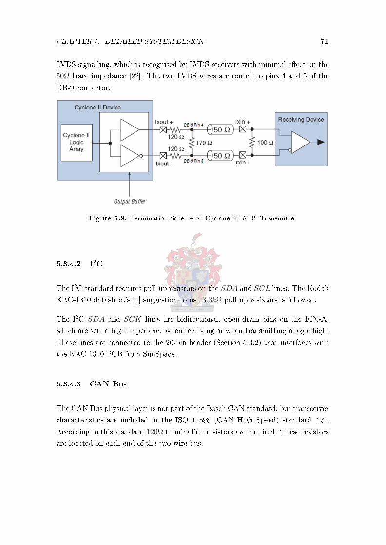
CHAPTER 5. DETAILED SYSTEM DESIGN 71
LVDS signalling, which is recognised by LVDS receivers with minimal eect on the
50Ω trace impedance [22]. The two LVDS wires are routed to pins 4 and 5 of the
DB-9 connector.
Figure 5.9: Termination Scheme on Cyclone II LVDS Transmitter
5.3.4.2 I2C
The I2C standard requires pull-up resistors on the SDA and SCL lines. The Kodak
KAC-1310 datasheet's [4] suggestion to use 3.3kΩ pull up resistors is followed.
The I2C SDA and SCK lines are bidirectional, open-drain pins on the FPGA,
which are set to high impedance when receiving or when transmitting a logic high.
These lines are connected to the 26-pin header (Section 5.3.2) that interfaces with
the KAC-1310 PCB from SunSpace.
5.3.4.3 CAN Bus
The CAN Bus physical layer is not part of the Bosch CAN standard, but transceiver
characteristics are included in the ISO 11898 (CAN High Speed) standard [23].
According to this standard 120Ω termination resistors are required. These resistors
are located on each end of the two-wire bus.

CHAPTER 5. DETAILED SYSTEM DESIGN 72
For testing of the CAN bus a PCAN-USB Adapter, from PEAK-System Technik,
will be used. PEAK-System Technik species that the CAN -low signal and the
CAN -high signal must be connected to pins 2 and 7 respectively, of the DB-9
connector [24]. Pin 6 is connected to ground.
5.3.5 Clock and Reset
The FPGA requires an external clock source to execute the synchronous design. A
66.666MHz clock oscillator is selected for this design. To generate the required clock
frequencies of 55.555MHz, 27.775MHz and 15.151MHz for the design, an internal
PLL of the Cyclone II FPGA is used.
Figure 5.10: Altera MegaWizard generated PLL with Locked signal output
This PLL is implemented using an Altera MegaWizard. See Figure 5.10. The PLL
locked signal is used as the global reset in the FPGA. This insures that the internal
state machines all reset and start simultaneously.

CHAPTER 5. DETAILED SYSTEM DESIGN 73
5.3.6 Power System
5.3.6.1 Power Regulators
The design requires three dierent supply voltages. A 3.3V supply is needed for
the NAND ash device, the CMOS image sensor, and some of the FPGA's I/O
pins. A 2.5V supply is needed for I/O Bank 8 of the FPGA to conform to the
LVDS signalling standard. The internal logic of the Cyclone II FPGA requires a
1.2V supply.
The preliminary specications of the design stated that the camera system should
operate from a power supply bus ranging anywhere between 5V and 12V. A Na-
tional Semiconductor LM2651 1.5A high eciency, synchronous switching regulator
is chosen to convert the 5-12V power bus to a 3.3V power level. The LM2651 can
handle an input voltage range of 4V to 14V and is capable of supplying up to 1.5A
at an eciency of nearly 97%. See Appendix G.1 and [25] for detailed information
on the LM2651.
The 2.5V power supply voltage is achieved by using a ST LF25CPT Very Low
Drop regulator [26], which is powered by the 3.3V power supply. The LF25CPT
has a Shutdown Logic Control function which makes it possible to put the device
in an inhibit state and eectively shutting the regulator down. This function is
used to power down I/O Bank 8 of the Cyclone II when LVDS is not in use. Refer
to Section 5.3.4.1.
A PowerPlay power analysis of the VHDL design in the Quartus II software stated
that IINT , of the Cyclone II EP2C35 FPGA, draws a maximum of 128.71mA during
operation. The Texas Instruments SN105125 150-mA Low Dropout regulator [27]
is selected as a suitable 1.2V power regulator and will also be powered from the
3.3V power supply.

CHAPTER 5. DETAILED SYSTEM DESIGN 74
5.3.6.2 Power planes
The PLL circuits in Cyclone II devices contain analogue components embedded
in the digital device [19]. These analogue components have separate 1.2V power,
VCCA PLL, and ground, GNDA, pins to minimize noise generated by the digital
components. A choke circuit is used to isolate the VCCA PLL and GNDA from the
power to the rest of the circuit. See Appendix F for details.
The PCB consists of four layers of which, the two internal layers are used as power
planes, while the two external layers are used for signalling. One of the internal
layers is a dedicated ground plane, with a GNDA power island for the analogue
PLL circuit. The other internal layer is a 3.3V power plane. This power plane
contains 1.2Vdigital, 1.2Vanalogue, and 2.5V power islands.
These ground and power planes distribute electrical power and heat better than
narrow tracks and minimise electromagnetic interference unintentionally formed by
the tracks.
5.3.7 Test Points and LEDs
To debug the circuit three status LEDs and multiple test points are added to the
PCB. The following test points are included in the design:
18 General-purpose test points on unused FPGA I/O pins,
Test points on all NAND ash device's pins,
Test points on all voltage levels, including ground, and
A test point on the clock oscillator's output.
The three LED's with current limiting resistors are:
A power indicator LED (green),

CHAPTER 5. DETAILED SYSTEM DESIGN 75
FPGA congured LED (yellow), and an
IP timeout indicator (red), also used as a `heartbeat' during debugging to
indicate that the design is downloaded to the FPGA correctly.
5.3.8 Device Placement and Routing
The I/O pins of the FPGA were manually grouped around the edges of the FPGA.
This was done to simplify routing and to keep tracks carrying similar signals the
same length. The propagation delay dierence, of the signals, is reduced by keeping
similar signal tracks the same length. I/O Bank 8 was used exclusively for the LVDS
signals as this I/O Bank is powered by the 2.5V power source.
When a PCB carries high frequencies, traces may need to be exact widths and
lengths to control the characteristic impedance of the traces. High-speed PCB
design is a specialised skill and therefore, after the circuit was designed and drawn
in Altium's Protel DXP 2004, the schematic was given to a layout specialist to
design the PCB.
The specialist did device placement, and matched the LVDS and CAN bus traces'
characteristic impedance to the standards supplied by SunSpace.
The prototype PCB can be seen in Figures 5.11 and 5.12.

CHAPTER 5. DETAILED SYSTEM DESIGN 76
Figure 5.11: Design routing and layout - Top layer
Figure 5.12: Design routing and layout - Bottom layer

Chapter 6
Simulations and Results
In this chapter, a report is given on the results and simulations for the system
design. The VHDL system design is tested by simulation for correct functionality.
The PCB is built and checked before a preliminary Nios II system is downloaded
to the Cyclone II. Interfacing to the KAC-1310 from the Nios II is then tested. An
initial Bad Block Table is created and a power analysis of the demonstration board
is done. A discussion on work in progress concludes the chapter.
6.1 VHDL Simulations
The correct functionality of the VHDL components can be simulated before they
are downloaded to the physical FPGA. Signals, internal to the FPGA and hidden
to the PCB, can be monitored within the simulator and speeds up development.
Altera's Quartus II 5.1 simulation software and ModelSim SE 5.8c were used to
simulate the design at various stages of development. All the simulations shown in
this chapter are gate-level timing simulations.
77

CHAPTER 6. SIMULATIONS AND RESULTS 78
6.1.1 Critical Test Simulations
Numerous simulations were done during the development of the system to ensure
functionality and it is impossible to show and discuss them all in this thesis. There-
fore, only critical test simulations are shown. These simulations demonstrate the
functionality of all the components with the help of examples.
6.1.1.1 Load Bad Block Table
A Load Bad Block Table sequence, refer to Section 5.1.1, demonstrates three key
parts of the design, namely a command decode, a page read, and an EDAC example.
Figures 6.1 and 6.2 illustrates the signal waveforms of a Load Bad Block Table
sequence. Figure 6.3 claries the simulation signal names. The paragraphs to
follow will discuss these signals in more detail.
Command Decode: The Image Exporter Module will only accept a new com-
mand when the readyNOTbusy signal is high. See Figure 6.1. The command
(51h = 01010001b) is latched when the cmd_enable signal is high. The rst 4 bits
in the command instruct that all the data must be routed to and from the Nios II.
The last 3 bits however override this instruction, as 001b indicates a Load BBT
command which forces the output of the Output-FIFO to be routed to the BBT
memory region. This can be seen in Figure 6.1 where the data_out_bbt bus is set
to 00h and the data_out_LVDS bus to high impedance (ZZ).
NAND Flash Read Page: The NAND Flash Read Page sequence is initiated
by pulling the ce signal low before the command 00h, 5 address cycles, and the
command 30h are written to the ash device. The 5 addresses are all 00h since
the BBT is loaded from block 0, page 0. The device goes into a busy state and
the ry_by signal is manually forced low for simulation purposes. When ry_by is
forced high, the data is read from the ash device into the Output-FIFO, one byte
at a time, by toggling the re signal.

CHAPTER 6. SIMULATIONS AND RESULTS 79
Figure 6.1: Load Bad Block Table Waveforms, Segment 1

CHAPTER 6. SIMULATIONS AND RESULTS 80
Figure 6.2: Load Bad Block Table Waveforms, Segment 2

CHAPTER 6. SIMULATIONS AND RESULTS 81
Figure 6.3: Block Diagram of Image Exporter with Simulation signal names
From the simulation, it can be seen that the following data is being loaded as the
BBT: 5Ah, 01h, 02h, 03h, etc. This is because a counter is used to fake the input
from the ash device, as no ash simulation model is available. In addition, a
normal BBT will mostly consist of 1's, which will make it dicult to distinguish
between individual bytes read from the device.
The 512 bytes of BBT data from the NAND ash will now be sequentially clocked
into the Output-FIFO, followed by 1536 dummy bytes and 12 ECC bytes. The
simulation waveforms continue on Figure 6.2
Error Detection and Correction: To illustrate that the EDAC operates cor-
rectly, the rst byte, read from the ash device, is injected with a one-bit error. The
read byte is 5Ah = 01011010b, but should be 58h = 01011000b according to the
ECC bytes read from the device on the data_io_nand bus, shown in Figure 6.2.
The 12 ECC bytes (55h, 55h, 59h, and nine 00h's) were computed for a data

CHAPTER 6. SIMULATIONS AND RESULTS 82
stream created from a counter, where the rst data 00h was replaced with 58h.
As seen in the simulation the bad_address and bad_strobe signals sends 4 bad
addresses (0001h, 1000h, 1000h and 1000h) to the Correction unit. Each address
indicates a possible bad byte in a 512-byte protected segment. The MSB (0b)
in 0001h indicates that a correctable error exists in the rst 512-byte protected
segment. The rest of the bits indicate that Byte 0, Bit 1 is at fault and needs to
be ipped. The correction can be seen on the data_out_bbt bus where 5Ah has
been corrected to 58h. The 1000h words indicate that no error or correctable error
exists in the following three 512-byte protected segments.
6.1.1.2 Store Bad Block Table
The Store Bad Block Table sequence, refer to Section 5.1.1, demonstrates a block
erase, status bit check and a page write.
After the Store Bad Block Table command (52h) is given, the Store Bad Block Table
sequence starts by ushing the BBT from the internal BBT memory into the Input-
FIFO, while simultaneously instructing the NAND Flash Interface module to erase
Block 0 of the ash device. See Figure 6.4. The 512 BBT bytes are followed by the
two 3-byte pointers used to store the last downloaded page- and last written page
addresses. Six demonstration pointer bytes (FCh, 01h, 02h, FFh, 04h and 05h)
can be seen in Figure 6.5 on the data_in_bbt bus.
NAND Flash Erase Block: Figure 6.4 also illustrates a ash block erase op-
eration. The ce signal is pulled low and the command 60h is written to the ash
device. As the column and page address is not needed, only three address cycles
are written to the device. The address cycles are all 00h since Block 0 is erased.
The address cycles are followed by the D0h command after which the device enters
a busy state (ry_by low) for a period of tBERS. This period can typically range be-
tween 2ms and 3ms. For demonstration purposes, this time was drastically reduced
to 80ns. The erase operation is complete when ry_by goes high.

CHAPTER 6. SIMULATIONS AND RESULTS 83
Figure 6.4: Store Bad Block Table Waveforms, Segment 1

CHAPTER 6. SIMULATIONS AND RESULTS 84
Figure 6.5: Store Bad Block Table Waveforms, Segment 2
Check Status Bit: Once the erase operation is complete a check status is per-
formed by writing a 70h command to the ash device. The status byte is read with
a toggle of the re signal. If the LSB of the read status byte is 0b then the erase
operation was successful.
NAND Flash Write Page: Figures 6.6 and 6.7 demonstrates a page write
operation. After the ce signal is pulled low the command 80h is written to the
ash device. The ve address cycles are all 00h since the BBT is stored in Block 0,
Page 0. The counter generated BBT data and 12 ECC bytes are now written one
byte at a time while toggling the we signal. To mark the end of the page and to
initiate the program operation, the 10h command is written to the ash device.
The device enters a busy state (ry_by low) for a period of tPROG, which can last

CHAPTER 6. SIMULATIONS AND RESULTS 85
Figure 6.6: Store Bad Block Table Waveforms, Segment 3

CHAPTER 6. SIMULATIONS AND RESULTS 86
Figure 6.7: Store Bad Block Table Waveforms, Segment 4
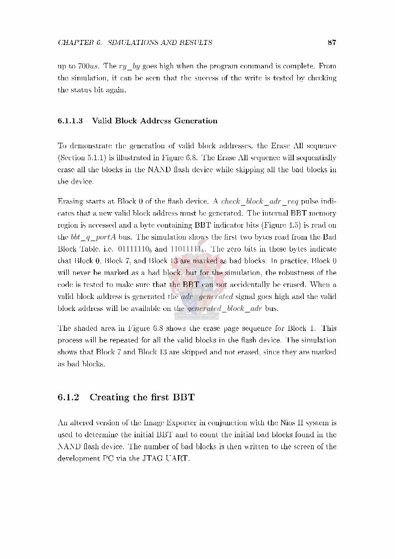
CHAPTER 6. SIMULATIONS AND RESULTS 87
up to 700us. The ry_by goes high when the program command is complete. From
the simulation, it can be seen that the success of the write is tested by checking
the status bit again.
6.1.1.3 Valid Block Address Generation
To demonstrate the generation of valid block addresses, the Erase All sequence
(Section 5.1.1) is illustrated in Figure 6.8. The Erase All sequence will sequentially
erase all the blocks in the NAND ash device while skipping all the bad blocks in
the device.
Erasing starts at Block 0 of the ash device. A check_block_adr_req pulse indi-
cates that a new valid block address must be generated. The internal BBT memory
region is accessed and a byte containing BBT indicator bits (Figure 4.5) is read on
the bbt_q_portA bus. The simulation shows the rst two bytes read from the Bad
Block Table, i.e. 01111110b and 11011111b. The zero bits in these bytes indicate
that Block 0, Block 7, and Block 13 are marked as bad blocks. In practice, Block 0
will never be marked as a bad block, but for the simulation, the robustness of the
code is tested to make sure that the BBT can not accidentally be erased. When a
valid block address is generated the adr_generated signal goes high and the valid
block address will be available on the generated_block_adr bus.
The shaded area in Figure 6.8 shows the erase page sequence for Block 1. This
process will be repeated for all the valid blocks in the ash device. The simulation
shows that Block 7 and Block 13 are skipped and not erased, since they are marked
as bad blocks.
6.1.2 Creating the rst BBT
An altered version of the Image Exporter in conjunction with the Nios II system is
used to determine the initial BBT and to count the initial bad blocks found in the
NAND ash device. The number of bad blocks is then written to the screen of the
development PC via the JTAG UART.
CHAPTER 6. SIMULATIONS AND RESULTS 88
Figure 6.8: Erase All Sequence Waveform
CHAPTER 6. SIMULATIONS AND RESULTS 89
Simulations indicated that this process should work, but in practice, some dicul-
ties were experienced when implemented on the demonstration board. It seemed
that the NAND ash device never returned from its busy state, because the R/B
pin would not return to logic high. It was discovered that the R/B pull-up resistor
was omitted from the schematic and PCB. After it was inserted, the NAND ash
device responded as expected.
Another problem surfaced, the Initial BBT Generator design reported that almost
all the blocks in the device were invalid! The reported number of bad blocks also
varied with every execution. Initially it was thought that timing errors were the
cause for these irregular results. A logic analyzer was hooked up to the test points
on the NAND ash chip. The logic analyzer showed that the signal timings were
correct and that hardly any initial bad blocks exist in the device. With the logic
analyzer, only blocks 1111, 3040, and 4062 were manually found as bad blocks.
The problem was thus localised in the VHDL code. After an in-depth inspection of
the code, it was realised that two state machines occasionally lost synchronisation
when the R/B line went high. This was an unforeseen case in the simulations, since
the R/B line was at all times controlled manually and not by a simulation model.
After both state machines were synchronised to the R/B line, the system reported
consistent results.
Eventually, ve bad blocks were found repeatedly in the NAND ash chip populated
on the demonstration board.
6.2 Nios II Simulations and Measurements
The Nios II IP is downloaded to the Cyclone II device via a JTAG cable. The Nios II
IP used for development is an evaluation version and requires the JTAG cable to
stay connected to the development board in order to prevent the Nios II IP to stop
functioning after one hour. Storing a Nios II IP core in the EPCS conguration
device is prohibited and this is enforced by the Altera software.
During implementation of the Nios II in hardware it was discovered that only a

CHAPTER 6. SIMULATIONS AND RESULTS 90
reduced driver set for the Nios II system can be downloaded to the Cyclone II,
since the Onboard Memory size is limited to 24Kbytes (Section 5.2.2.2). The main
drawback of a reduced driver set is that drivers, relying on software functions based
on the getc command in ANSI C, are omitted. Consequently, the host PC is not
able to emulate an OBC by sending commands via the JTAG UART and thus
facilitates only one-way communication from the Nios II to the host PC.
The Nios II processor, executing code, can be simulated in ModelSim. This is useful
to determine Avalon bus access times to User Logic components, as information on
this topic is limited. Figure 6.9 shows an example where the CMOS Image Sensor
Interface's FIFO is accessed. This buer FIFO was packed with dummy counter
bytes and its output can be seen on the readdata bus. The example also illustrates
the speed (486ns/word) at which 32-bit words can be transferred from User Logic
to Onboard Memory.
6.3 Kodak KAC-1310 Interfacing
The CMOS Image Sensor Interface and the I2C Module is used to access the KAC-
1310 from the Nios II. The CMOS Image Sensor Interface needs to generate a
MCLK for the operation of the KAC-1310. Due to timing constraints, the Quartus
tter program can not implement a working MCLK slower than 1.26MHz, from the
15.151MHz clock supplied by the PLL. This poses no problem as the pixel data
rate, of 1.19MB/s, can easily be handled when the KAC-1310 is clocked with a
MCLK of 1.26MHz.
The CMOS Image Sensor Interface initialises the KAC-1310 by pulling the KAC-
1310's INIT pin high for 1ms and low for a further 1ms.
The I2C Module is used for communication between the Nios II and KAC-1310.
However the I2C Module software drivers had to be altered because the command
sequences did not comply with the KAC-1310's specications. The SCL frequency
was also set in software to 50kHz as the KAC-1310 is a slave device that supports a
maximum clock rate (SCL) of 1/24th MCLK [4]. The I2C signals were scrutinized

CHAPTER 6. SIMULATIONS AND RESULTS 91
Figure 6.9: Avalon access times to CMOS Image Sensor Interface Module

CHAPTER 6. SIMULATIONS AND RESULTS 92
with the help of an oscilloscope and found to operate perfectly. The setup regis-
ters in the KAC-1310 were updated successfully via the I2C bus as the KAC-1310
responded as expected.
Figure 6.10: Sub-sampled photo taken with the camera system (160×100 pixels)
When the KAC-1310 is instructed, via I2C, to capture a sub-sampled image, pixel
data can be seen on the pixel data bus with an oscilloscope. The FIFO in the
CMOS Image Sensor Interface latches these bytes and the Nios II outputs the data
to the host PC via the JTAG UART. Unfortunately, the image received does not
look like a photo, as shown in Figure 6.10.
To isolate the problem the input to the FIFO, in the CMOS Image Sensor Interface,
was replaced with a counter that increments on every rising edge of the received
HCLK. The counter data read from the FIFO to the host PC proved to be correct
and the problem was isolated to the latching of unsynchronised signals, external to
the FPGA. This debugging process was still in progress at the time of writing this
thesis.

CHAPTER 6. SIMULATIONS AND RESULTS 93
6.4 Demonstration Board Testing and
Measurements
During the manufacturing of the PCB, two copies of the same PCB were made
to test the demonstration board systematically. After testing the blank PCB for
short circuits, the rst demonstration board was populated with the complete power
supply. This includes all the power regulators, necessary capacitors, inductors, and
resistors. The clock oscillator chip was also mounted on the board. All the power
regulators were successfully tested to output the correct voltage levels.
The clock oscillator provides a perfect 66.666MHz sinusoidal waveform. An oscil-
loscope with an FFT function was used to see if the clock oscillator added any
intolerable noise harmonics to the power rails. As the clock's interference were
found to be negligible (-50dB for the rst harmonic measured on the 3.3V power
plane) it was decided to populate the second board with the Cyclone II.
To ease the placing of the BGA packaged Cyclone II the second board was at
rst only populated with the Cyclone II's decoupling capacitors, after which the
Cyclone II FPGA was placed on the PCB. This was done so that conducted heat
would not violate the integrity of the BGA ball connections during soldering of the
remaining components.
All the remaining components apart from the NAND ash chip were soldered onto
the second demonstration PCB. The functionality of the Cyclone II was veried
before the NAND ash chip was added. The Cyclone II and the EPCS conguration
device were conrmed to work by loading the EPCS conguration device with a
simple heartbeat design. The heartbeat design ashes a LED on and o and worked
since the rst time it was loaded.
Designs that are more complex were progressively loaded onto the FPGA and
incrementally tested, until the camera design was complete. The full design uses
22% of the total logic elements in the Cyclone II, which leaves ample space for
potential expansions.

CHAPTER 6. SIMULATIONS AND RESULTS 94
6.4.1 Power and Area Calculations
Area The dimensions of the demonstration PCB are 67mm × 69mm equalling
an area of 46.23cm2 while the SunSpace KAC-1310 PCB measures 32mm×45mm,
equalling an area of 14.4cm2. The total design thus have a remarkably compact
area of 60.63cm2.
Power The demonstration board's power consumption was measured with only
the power supply unit and clock oscillator installed on the board. This yielded a
power usage of 63mW . After the remaining components were added to the board
and the heartbeat design was running on the system, the power usage increased to
534mW .
When the KAC-1310 board was connected to the demonstration board the power
usage increased to 910mW . The Nios II was then instructed to initialise the KAC-
1310 and the power consumption surged to a further 1.376W . This power usage
was drastically reduced to 973mW when the KAC-1310 was instructed to make use
of an external bias resistor and to operate in the Soft Standby mode [4].
It is interesting to note that the power consumption of the camera system drops
to 852mW while the Nios II waits for data from the Avalon bus. This is probably
because the Nios II's pipeline stalls until data arrives.
The demonstration board contains three LEDs, each consuming 7mW , 21mW in
total, and this excess power can be subtracted from the system's total power usage.
The system's peak power consumption is thus 952mW and this is below the required
power usage of 1W .
During power cycling of the camera system onboard the nanosatellite it is expected
that the camera will not operate longer than 1.5 seconds at a time. Consuming
952mW at peak for 1.5 seconds gives a rating of 397µWh, which is exceptionally
low. If this camera system were to operate from a Nickel Metal Hydride (NiMH)
2300mAh, 1.5V AA Rechargeable Battery it would be able to take one photo, every
hour, for 362 days without the need to recharge the battery. This performance is
ideal for a subsystem onboard a nanosatellite.

CHAPTER 6. SIMULATIONS AND RESULTS 95
6.5 Work in progress
The camera system does not take proper photos and this need to be corrected. As
mentioned before the debugging process was still in progress at the time of writing.
The next step in the debugging process would be to route counter bit lines out of
the FPGA and back into the I/O pins of the buer FIFO. By doing this, known
data can be latched by the FIFO and hopefully, the error can be identied and
corrected.
The Opencores.org open-source CAN bus module, selected for this design, lacks
documentation and the code is written in Verilog. The CAN bus core has not been
implemented on the FPGA as there was no time for the author to learn Verilog.
Further research on other available CAN bus cores needs to be done or Verilog must
be studied if the cheaper option is to be followed.Also CAN transceivers need to
be implemented in hardware, which is required to perform the bit-wise arbitration
by producing dominant and recessive bits on the bus.
Currently the LVDS downlink has not been tested in hardware, as no LVDS receiver
device was available for testing. The LVDS transmitter is provided by Altera and
it should work when tested in the future.

Chapter 7
Conclusions and Recommendations
7.1 Conclusions
In this thesis, a camera system for a nanosatellite based on a CMOS image sensor
is designed. The design specications and constraints were investigated. A ver-
satile design was proposed where all the required functions are implemented on a
single FPGA. This includes BBT management, data routing, an EDAC, a soft-core
processor, glue logic to external devices, and communication busses. Low power
and compact devices were selected to minimize the power usage and the physical
size of the camera system.
The Altera Nios II/f soft-core processor was implemented as a controller for its
high processing speed and fast access time to other on-chip components. Using a
processor enables changes to the system to be easily made in software.
An alternative solution for transferring image data from the Nios II was found
when the DMA controller could not be implemented due to memory limitations.
The Nios II manually transfers the data from memory, while the data received
from the KAC-1310 is buered in a FIFO. Simulations of the Nios II processor
determined its access times to external logic enabling the minimum depth of this
FIFO to be derived.
96

CHAPTER 7. CONCLUSIONS AND RECOMMENDATIONS 97
Although the author had no real previous experience with VHDL, VHDL logic
components were developed to be interfaced with the Nios II system. All these
components conform to the Avalon slave standard.
The NAND ash memory size was selected large enough making the camera system
capable of storing more than a 100, 1024× 1024 pixel, images. To make the mass
memory more robust against radiation and random bit ips, a Hamming EDAC
scheme was implemented in VHDL.
The occurrence of bad blocks during the lifetime of a NAND ash device posed an
internal address generation problem. This was solved with an 8 × 512 bit lookup
table, which enables the status of every block to be represented as valid or invalid.
By mapping out all the bad block addresses, the memory space appears continuous.
Wear levelling is accomplished by writing and erasing all blocks equally often.
One of the main challenges of this design was to transfer data from the CMOS
image sensor to the NAND ash memory device, while simultaneously downloading
images from the NAND ash memory. Dual-clock FIFOs were implemented to shift
the data around, making it possible to input data into the FIFO at one particular
data rate while concurrently outputting data from the FIFO at a dierent data
rate.
Components used on a nanosatellite must use power conservatively. Power regu-
lators were chosen for their high eciency and compactness. The system's peak
power consumption is 952mW which is below the required power usage of 1W
making it ideal for a subsystem onboard a nanosatellite.
Although the project was cut short before the camera system could operate 100% as
intended, most of the system requirements were met. In addition, a good mixture
of IP soft-cores, open-source cores, and user created logic are utilised in this broad
base design, containing a combination of hardware, digital logic, and software.
The design was kept both simple and modular for straightforward upgrades and
maintenance in the future.

CHAPTER 7. CONCLUSIONS AND RECOMMENDATIONS 98
7.2 Recommendations
The following recommendations are made with regards to the future development
of a camera system unit for the nanosatellite using a CMOS Image Sensor and
NAND ash memory:
ECC can be done on smaller partitions, resulting in an even more reliable
data storage system.
A backup of the original BBT can be stored in the second page of block 0 for
redundancy.
A simple DMA controller can be written in VHDL to relieve the workload on
the Nios II processor.
The LVDS download speed can be made adjustable for simpler interfacing
with slower systems.
Finally, complete functional-, radiation- and extreme temperature testing of the
demonstration board will give valuable information on how the camera system
might operate in a space environment.

List of References
[1] Wertz, J.R. and Larson, W.J.: Space Mission Analysis and Design. Space
Technology Library, 3rd edn. Microcosm Press and Kluwer Academic Publishers, El
Segundo, California, 1999.
[2] Bryer, B.: Protection Unit for Radiation Induced Errors in Flash Memory Systems.
Master's thesis, University of Stellenbosch, 2004.
[3] Horsburgh, I.J.: The Development of a Mass Memory Unit for a Micro-Satellite
using NAND Flash Memory. Master's thesis, University of Stellenbosch, 2005.
[4] Kodak: KODAK KAC-1310 Image Sensor. Tech. Rep., Kodak, 2002.
[5] Samsung: 512M x 8 Bit / 1G x 8 Bit NAND Flash Memory. Tech. Rep., Samsung
Electronics, 2005.
[6] Altera: Avalon Interface Specication. Altera Corporation, San Jose, CA, 3rd edn,
2005. mnl_avalon_spec.pdf.
[7] Altera: Nios II Processor Reference Handbook. Altera Corporation, San Jose, CA,
6th edn, 2006. n2cpu_nii51001.pdf.
[8] Kalinsky, D. and Kalinsky, R.: Introduction to I2C. www.embedded.com, July
2001. http://www.embedded.com/story/OEG20010718S0073.
[9] Laboratory of Architecture of the Processors FPSL: Fiche technique du module
I2C. Tech. Rep., Federal Polytechnic School of Lausanne, Switzerland, 2005.
[10] The Free Encyclopedia. www.wikipedia.org, 2005-2006.
99

LIST OF REFERENCES 100
[11] National Semiconductor Corporation: National announces rst implementation of
new IEEE and TIA LVDS (Low Voltage Dierential Signal) standard.
www.national.com/news, April 1996.
http://www.national.com/news/1995/9502/dm95001dtp.html.
[12] Altera: Error Detection & Recovery Using CRC in Altera FPGA Devices. Altera
Corporation, San Jose, CA, 1st edn, 2006. an357.pdf.
[13] Memory Product & Technology Division: APPLICATION NOTE for NAND Flash
Memory. Samsung Electronics, 2nd edn, 1999.
[14] Memory Division Samsung Electronics: NAND Flash Spare Area Assignment
Standard. Samsung Electronics, February 2003.
spare_assignment_standard_20030221.pdf.
[15] Altera: Designing With High-Density BGA Packages for Altera Devices. Altera
Corporation, San Jose, CA, 4th edn, 2006. n2cpu_nii5v3.pdf.
[16] Altera: Nios II Flash Programmer User Guide. Altera Corporation, San Jose, CA,
1st edn, 2005. Ug_nios2_ash_programmer.pdf.
[17] Altera: Developing Peripherals for SOPC Builder. Altera Corporation, San Jose,
CA, 1st edn, 2004. an333.pdf.
[18] Altera: Designing With High-Density BGA Packages for Altera Devices. Altera
Corporation, San Jose, CA, 4th edn, 2006. an114.pdf.
[19] Altera: Cyclone Device Handbook, Volume 1. Altera Corporation, San Jose, CA,
1st edn, 2005. cyc_c5v1.pdf.
[20] Altera: Altera Conguration Devices. Altera Corporation, San Jose, CA, 2nd edn,
2005. cfg_ch1_vol_2 - Cong handbook Vol 2.
[21] Altera: Serial Conguration Devices (EPCS1, EPCS4, EPCS16 & EPCS64)
Features. Altera Corporation, San Jose, CA, 2nd edn, 2005. cyc_c51014 - Cong
handbook Vol2 Ch4.pdf.
[22] Altera: Cyclone II Device Handbook, Volume 1. Altera Corporation, San Jose, CA,
2nd edn, 2005. cyc2_cii5v1.pdf.

LIST OF REFERENCES 101
[23] Nilsson, S.: Controller area network - can information.
http://www.algonet.se/staann/developer/CAN.htm, June 1997.
[24] PEAK System Technik: PCAN-USB Adaptor Hardware Manual. PEAK System
Technik GmbH, Darmstadt, Germany, 1.3 edn, 2002. PCAN-USB_ENG.pdf.
[25] National Semiconductor: LM2651 1.5A High Eciency Synchronous Switching
Regulator. Tech. Rep., National Semiconductor Corporation, 2005.
[26] ST: LF00 Series - Very Low Drop Voltage Regulators with Inhibit. Tech. Rep., ST,
2004.
[27] Texas Instruments: SN105125 150-mA Low Dropout Regulator with POK. Tech.
Rep., Texas Instruments Incorporated, 2002.

Appendices
102

Appendix A
Kodak KAC-1310 Datasheet
103

APPENDIX A. KODAK KAC-1310 DATASHEET 104
Figure A.1: Kodak KAC-1310 CMOS Image Sensor Datasheet, Page 5 [4]

Appendix B
Samsung K9K4G08U0M Datasheet
105

APPENDIX B. SAMSUNG K9K4G08U0M DATASHEET 106
Figure B.1: Samsung K9K4G08U0M NAND Flash Datasheet, Page 2 [5]

Appendix C
imageexporter_regs.h
/* Eric Baker - 2006/01/19 */
#ifndef __IMAGEEXPORTER_REGS_H__
#define __IMAGEEXPORTER_REGS_H__
#include <io.h>
// Register Addresses
#define IE_COMMAND 0
#define IE_DATA 1
#define IE_STATUS 2
//Read from Image Exporter
#define IORD_IE(base , offset) IORD(base , offset)
// Write to Image Exporter
#define IOWR_IE(base , offset , data) IOWR(base , offset , data)
// input select bits mask
#define IMAGE_EXPORTER_COMMAND_INPUT_SELECT_MSK (0xC0) // 11000000
#define IMAGE_EXPORTER_COMMAND_INPUT_SELECT_OFST (6)
// output select bits mask
#define IMAGE_EXPORTER_COMMAND_OUTPUT_SELECT_MSK (0x30) // 00110000
#define IMAGE_EXPORTER_COMMAND_OUTPUT_SELECT_OFST (4)
// buffer in FIFO bit mask
#define IMAGE_EXPORTER_COMMAND_inFIFO_BUFFER_MSK (0x08) // 00001000
#define IMAGE_EXPORTER_COMMAND_inFIFO_BUFFER_OFST (3)
107

APPENDIX C. IMAGEEXPORTER_REGS.H 108
// instruction bits mask
#define IMAGE_EXPORTER_COMMAND_INSTRUCTION_MSK (0x07) // 00000111
#define IMAGE_EXPORTER_COMMAND_INSTRUCTION_OFST (0)
// status bits mask
#define IMAGE_EXPORTER_STATUS_FLASH_BUSY_MSK (0x01) // 00000001
#define IMAGE_EXPORTER_STATUS_FLASH_BUSY_OFST (0)
#define IMAGE_EXPORTER_STATUS_inFIFO_HALF_FULL_MSK (0x02) // 00000010
#define IMAGE_EXPORTER_STATUS_inFIFO_HALF_FULL_OFST (1)
#define IMAGE_EXPORTER_STATUS_inFIFO_FULL_MSK (0x04) // 00000100
#define IMAGE_EXPORTER_STATUS_inFIFO_FULL_OFST (2)
#define IMAGE_EXPORTER_STATUS_outFIFO_EMPTY_MSK (0x08) // 00001000
#define IMAGE_EXPORTER_STATUS_outFIFO_EMPTY_OFST (3)
#define IMAGE_EXPORTER_STATUS_FLASH_FULL_MSK (0x10) // 00010000
#define IMAGE_EXPORTER_STATUS_FLASH_FULL_OFST (4)
#define IMAGE_EXPORTER_STATUS_ALL_IMAGES_DOWNLOADED_MSK (0x20) // 00100000
#define IMAGE_EXPORTER_STATUS_ALL_IMAGES_DOWNLOADED_OFST (5)
// Constants
#define IMAGE_EXPORTER_INPUT_CAMERA (0x0) //0000
#define IMAGE_EXPORTER_INPUT_NIOS (0x1) //0001
#define IMAGE_EXPORTER_OUTPUT_LVDS (0x0) //0000
#define IMAGE_EXPORTER_OUTPUT_NIOS (0x1) //0001
#define IMAGE_EXPORTER_inFIFO_BUFFER_ENABLE 0
#define IMAGE_EXPORTER_inFIFO_BUFFER_DISABLE 1
#define IMAGE_EXPORTER_LOAD_BTT (0x1) //0001
#define IMAGE_EXPORTER_STORE_BTT (0x2) //0010
#define IMAGE_EXPORTER_ERASE_FLASH (0x3) //0011
#define IMAGE_EXPORTER_WRITE_PAGE (0x4) //0100
#define IMAGE_EXPORTER_READ_PAGE (0x5) //0101
#define IMAGE_EXPORTER_RESET_FLASH (0x6) //0110
#endif /* __IMAGE_EXPORTER_REGS_H__ */

Appendix D
image_exporter_avalon_interface.vhd
--Eric Baker
--13 January 2006
LIBRARY ieee;
USE ieee.STD_LOGIC_1164.ALL;
USE ieee.STD_LOGIC_unsigned.ALL;
USE ieee.numeric_std.ALL;
ENTITY image_exporter_avalon_interface is
PORT (
--inputs:
address : IN STD_LOGIC_VECTOR (1 DOWNTO 0);
chipselect : IN STD_LOGIC;
clk : IN STD_LOGIC;
reset : IN STD_LOGIC;
write : IN STD_LOGIC;
writedata : IN STD_LOGIC_VECTOR (7 DOWNTO 0);
read : IN STD_LOGIC;
--outputs:
irq : OUT STD_LOGIC;
readdata : OUT STD_LOGIC_VECTOR (7 DOWNTO 0);
--exports:
clk55M : IN STD_LOGIC; --from pll
--Interface with NAND Flash lines
data_nand : INOUT STD_LOGIC_VECTOR (7 DOWNTO 0); --Bidirectional data lines
ry_by : IN STD_LOGIC; --Ready/busy line
ale : OUT STD_LOGIC; --Address latch enable
cle : OUT STD_LOGIC; --Command Latch enable
109

APPENDIX D. IMAGE_EXPORTER_AVALON_INTERFACE.VHD 110
we : OUT STD_LOGIC; --Write enable
re : OUT STD_LOGIC; --Read enable
wp : OUT STD_LOGIC; --Write Protect
ce : OUT STD_LOGIC; --Chip enable
--Data in
data_in_camera : IN STD_LOGIC_VECTOR (7 DOWNTO 0);
--Data out
data_out_LVDS : OUT STD_LOGIC_VECTOR (7 DOWNTO 0);
data_out_strobe : OUT STD_LOGIC;
--test signals
l_wrt_p_a ,
l_dwn_p_a : OUT STD_LOGIC_VECTOR (17 DOWNTO 0);
adr_generatedt ,
lastblk ,
ck_blk_adr_rq : OUT STD_LOGIC;
block_adrt : OUT STD_LOGIC_VECTOR (11 DOWNTO 0);
bb_qat ,bb_qbt : OUT STD_LOGIC_VECTOR (7 DOWNTO 0);
rdreq_outQt : OUT STD_LOGIC;
dout2 ,dout3 ,dout4 ,
data_out_bbt ,
data_in_bbt : OUT STD_LOGIC_VECTOR (7 DOWNTO 0);
bad_addresst : OUT STD_LOGIC_VECTOR (12 DOWNTO 0);
bad_strobet : OUT STD_LOGIC;
cor_readyt ,
clk_outt : OUT STD_LOGIC;
wr_fifo ,wr_flash : OUT STD_LOGIC
);
END ENTITY image_exporter_avalon_interface;
ARCHITECTURE image_exporter_avalon_interface_architecture
OF image_exporter_avalon_interface IS
COMPONENT image_exporter IS
PORT(
clk55M :IN STD_LOGIC; --55MHz ClK in
clk :IN STD_LOGIC; --27.5 MHz Clk in
reset :IN STD_LOGIC; --Global Reset
--Interface with NAND Flash lines
data_nand :INOUT STD_LOGIC_VECTOR (7 DOWNTO 0); --Bidirectional data lines
ry_by :IN STD_LOGIC; --Ready/busy line
ale :OUT STD_LOGIC; --Address latch enable
cle :OUT STD_LOGIC; --Command Latch enable
we :OUT STD_LOGIC; --Write enable
re :OUT STD_LOGIC; --Read enable
wp :OUT STD_LOGIC; --Write Protect
ce :OUT STD_LOGIC; --Chip enable
--Control from NIOS
command :IN STD_LOGIC_VECTOR (7 DOWNTO 0); -- command from NIOS

APPENDIX D. IMAGE_EXPORTER_AVALON_INTERFACE.VHD 111
-- Input_sel [7..6]| Output_sel [5..4]| Buffer_Image [3]| Instr [2..0]
cmd_ena :IN STD_LOGIC; -- accept command from NIOS
--Warnings to NIOS
readyNOTbusy :OUT STD_LOGIC; -- is system executing a command , ie. ready not busy
all_downloaded :OUT STD_LOGIC; -- all pages in flash have been downloaded
all_written :OUT STD_LOGIC; -- all pages in flash have been written
rdempty_outQ :OUT STD_LOGIC;
wrfull_inQ :OUT STD_LOGIC;
fifo_half_full :OUT STD_LOGIC; --Interupt for NIOS to start Writing page to Flash
--Data in
data_in_camera :IN STD_LOGIC_VECTOR (7 DOWNTO 0);
data_in_nios :IN STD_LOGIC_VECTOR (7 DOWNTO 0);
--Data out
data_out_LVDS :OUT STD_LOGIC_VECTOR (7 DOWNTO 0);
data_out_nios :OUT STD_LOGIC_VECTOR (7 DOWNTO 0);
data_out_strobe :OUT STD_LOGIC;
--test signals
l_wrt_p_a ,
l_dwn_p_a :OUT STD_LOGIC_VECTOR (17 DOWNTO 0);
adr_generatedt ,
lastblk ,
ck_blk_adr_rq :OUT STD_LOGIC;
block_adrt :OUT STD_LOGIC_VECTOR (11 DOWNTO 0);
bb_qat ,bb_qbt :OUT STD_LOGIC_VECTOR (7 DOWNTO 0);
rdreq_outQt :OUT STD_LOGIC;
dout2 ,dout3 ,dout4 ,
data_out_bbt ,
data_in_bbt :OUT STD_LOGIC_VECTOR (7 DOWNTO 0);
bad_addresst :OUT STD_LOGIC_VECTOR (12 DOWNTO 0);
bad_strobet :OUT STD_LOGIC;
cor_readyt ,
clk_outt :OUT STD_LOGIC;
wr_fifo ,wr_flash :OUT STD_LOGIC
);
END COMPONENT image_exporter;
SIGNAL status_vector ,status_vector_old : STD_LOGIC_VECTOR (7 DOWNTO 0);
SIGNAL command , data_in_nios ,data_out_nios : STD_LOGIC_VECTOR (7 DOWNTO 0);
SIGNAL cmd_ena : STD_LOGIC;
SIGNAL readyNOTbusy ,
all_downloaded ,
all_written ,
rdempty_outQ ,
wrfull_inQ ,
fifo_half_full : STD_LOGIC;
BEGIN
status_vector <= "00" & all_downloaded & all_written & rdempty_outQ & wrfull_inQ
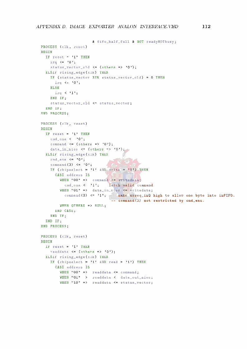
APPENDIX D. IMAGE_EXPORTER_AVALON_INTERFACE.VHD 112
& fifo_half_full & NOT readyNOTbusy;
PROCESS (clk , reset)
BEGIN
IF reset = '1' THEN
irq <= '0';
status_vector_old <= (others => '0');
ELSIF rising_edge(clk) THEN
IF (status_vector XOR status_vector_old) = 0 THEN
irq <= '0';
ELSE
irq <='1';
END IF;
status_vector_old <= status_vector;
END IF;
END PROCESS;
PROCESS (clk , reset)
BEGIN
IF reset = '1' THEN
cmd_ena <= '0';
command <= (others => '0');
data_in_nios <= (others => '0');
ELSIF rising_edge(clk) THEN
cmd_ena <= '0';
command (3) <= '0';
IF (chipselect = '1' AND write = '1') THEN
CASE address IS
WHEN "00" => command <= writedata;
cmd_ena <= '1'; -- latch valid command
WHEN "01" => data_in_nios <= writedata;
command (3) <= '1'; -- make wrreq_inQ high to allow one byte into inFIFO.
-- command (3) not restricted by cmd_ena.
WHEN OTHERS => NULL;
END CASE;
END IF;
END IF;
END PROCESS;
PROCESS (clk , reset)
BEGIN
IF reset = '1' THEN
readdata <= (others => '0');
ELSIF rising_edge(clk) THEN
IF (chipselect = '1' AND read = '1') THEN
CASE address IS
WHEN "00" => readdata <= command;
WHEN "01" => readdata <= data_out_nios;
WHEN "10" => readdata <= status_vector;

APPENDIX D. IMAGE_EXPORTER_AVALON_INTERFACE.VHD 113
WHEN OTHERS => NULL;
END CASE;
END IF;
END IF;
END PROCESS;
ei : image_exporter PORT MAP (clk55M ,
clk ,
reset ,
data_nand ,
ry_by ,
ale ,
cle ,
we,
re,
wp,
ce,
command ,
cmd_ena ,
readyNOTbusy ,
all_downloaded ,
all_written ,
rdempty_outQ ,
wrfull_inQ ,
fifo_half_full ,
data_in_camera ,
data_in_nios ,
data_out_LVDS ,
data_out_nios ,
data_out_strobe ,
l_wrt_p_a , l_dwn_p_a ,
adr_generatedt ,lastblk ,ck_blk_adr_rq ,
block_adrt ,
bb_qat ,bb_qbt ,
rdreq_outQt ,
dout2 ,dout3 , dout4 , data_out_bbt ,data_in_bbt ,
bad_addresst ,
bad_strobet ,
cor_readyt ,clk_outt ,
wr_fifo ,wr_flash
);
END ARCHITECTURE image_exporter_avalon_interface_architecture;

Appendix E
cmosimager.c
/* -----------------------------------------------------------------
* Eric Baker - 2 June 2006
*-----------------------------------------------------------------
* cmosimager.c - Camera 2D interface library
*-----------------------------------------------------------------*/
#include "cmosimager.h"
#include "i2c.h"
#include "imageexporter.h"
#include "system.h"
#include "io.h"
#define page_size 2048
#define image_width 1280
#define image_height 1024
#define image_size image_width*image_height
#define page_total image_size/page_size
#define longbyte_total page_size /4
#define wait_millisec int i; for (i=0; i<(3* ALT_CPU_FREQ /1000);) i++;
/*
* Standard configuration for KAC -1310
*/
void cmos_imager_configure(int base)
/* Make sure that the INIT pin is high for at least 1ms */
IOWR_CMOS(base , CMOS_STANDBY , 0x00);
wait_millisec;
/* Start Initialisation by making INIT pin low for 1ms */
114
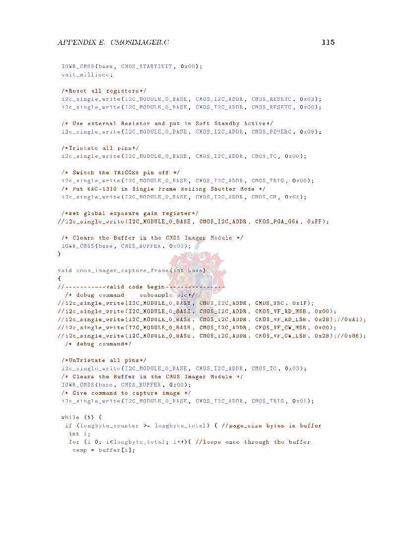
APPENDIX E. CMOSIMAGER.C 115
IOWR_CMOS(base , CMOS_STARTINIT , 0x00);
wait_millisec;
/* Reset all registers */
i2c_single_write(I2C_MODULE_0_BASE , CMOS_I2C_ADDR , CMOS_RESETC , 0x03);
i2c_single_write(I2C_MODULE_0_BASE , CMOS_I2C_ADDR , CMOS_RESETC , 0x00);
/* Use external Resistor and put in Soft Standby Active */
i2c_single_write(I2C_MODULE_0_BASE , CMOS_I2C_ADDR , CMOS_POWERC , 0x09);
/* Tristate all pins*/
i2c_single_write(I2C_MODULE_0_BASE , CMOS_I2C_ADDR , CMOS_TC , 0x00);
/* Switch the TRIGGER pin off */
i2c_single_write(I2C_MODULE_0_BASE , CMOS_I2C_ADDR , CMOS_TRIG , 0x00);
/* Put KAC -1310 in Single Frame Rolling Shutter Mode */
i2c_single_write(I2C_MODULE_0_BASE , CMOS_I2C_ADDR , CMOS_CM , 0x6A);
/*set global exposure gain register */
// i2c_single_write(I2C_MODULE_0_BASE , CMOS_I2C_ADDR , CMOS_PGA_GGA , 0xFF);
/* Clears the Buffer in the CMOS Imager Module */
IOWR_CMOS(base , CMOS_BUFFER , 0x00);
void cmos_imager_capture_frame(int base)
// -----------valid code begin ----------------
/* debug command - subsample pic*/
// i2c_single_write(I2C_MODULE_0_BASE , CMOS_I2C_ADDR , CMOS_SSC , 0x1F);
// i2c_single_write(I2C_MODULE_0_BASE , CMOS_I2C_ADDR , CMOS_VF_RD_MSB , 0x00);
// i2c_single_write(I2C_MODULE_0_BASE , CMOS_I2C_ADDR , CMOS_VF_RD_LSB , 0x28 );//0 xA1);
// i2c_single_write(I2C_MODULE_0_BASE , CMOS_I2C_ADDR , CMOS_VF_CW_MSB , 0x00);
// i2c_single_write(I2C_MODULE_0_BASE , CMOS_I2C_ADDR , CMOS_VF_CW_LSB , 0x28 );//0 x86);
/* debug command */
/* UnTristate all pins*/
i2c_single_write(I2C_MODULE_0_BASE , CMOS_I2C_ADDR , CMOS_TC , 0x03);
/* Clears the Buffer in the CMOS Imager Module */
IOWR_CMOS(base , CMOS_BUFFER , 0x00);
/* Give command to capture image */
i2c_single_write(I2C_MODULE_0_BASE , CMOS_I2C_ADDR , CMOS_TRIG , 0x01);
while (1)
if (longbyte_counter >= longbyte_total) // page_size bytes in buffer
int i;
for (i=0; i<longbyte_total; i++) // loops once through the buffer
temp = buffer[i];

APPENDIX E. CMOSIMAGER.C 116
IOWR_IE(base ,IE_DATA ,( unsigned char)temp);
temp = temp >>8; // shifts 32bit register to get next byte.
IOWR_IE(base ,IE_DATA ,( unsigned char)temp);
temp = temp >>8;
IOWR_IE(base ,IE_DATA ,( unsigned char)temp);
temp = temp >>8;
IOWR_IE(base ,IE_DATA ,( unsigned char)temp);
/* check these out: memcpy (0,0,0); memset , bcopy*/
page_counter ++;
if (page_counter >= page_total )
page_counter = 0;
return; //one image saved to mass storage
longbyte_counter = 0;
else
while (IORD_CMOS(base , CMOS_BUFFER ));//insert image processing code here
buffer[longbyte_counter] = IORD_CMOS(base , CMOS_READDATA );
longbyte_counter ++;

Appendix F
Demonstration Board Schematics
This appendix contains the PCB schematics for the camera demonstration board.
117

APPENDIX F. DEMONSTRATION BOARD SCHEMATICS 118
11
22
33
44
DD
CC
BB
AA
Title
Num
ber
Rev
isio
nSi
ze A4
Dat
e:20
06/0
9/30
Shee
t o
f Fi
le:
C:\D
ocum
ents
and
Set
tings
\..\T
op.S
CH
DO
CDra
wn
By:
nCSOASDO
CM
OS_
PIX
9
CM
OS_
PIX
0C
MO
S_PI
X1
CM
OS_
PIX
2C
MO
S_PI
X3
CM
OS_
PIX
4C
MO
S_PI
X5
CM
OS_
PIX
6C
MO
S_PI
X7
CM
OS_
PIX
8
TIM
EOU
T
CM
OS_
SDA
CM
OS_
SCL
DA
TA_O
UT
CM
OS_
TRIG
CM
OS_
INIT
CM
OS_
MC
LK
CA
N_L
OW
CA
N_H
IGH
CR
C_ER
RO
R
CM
OS_
DS1
W-D
O
FPG
A_a
b.sc
hdoc
NA
ND
_IO
0N
AN
D_I
O1
NA
ND
_IO
2N
AN
D_I
O3
NA
ND
_IO
4N
AN
D_I
O5
NA
ND
_IO
6N
AN
D_I
O7
LVD
S_tx
out(p
)LV
DS_
txou
t(n)
NA
ND
_nR
EN
AN
D_n
CE
NA
ND
_CLE
NA
ND
_ALE
NA
ND
_nW
EN
AN
D_n
WP
FPG
A_c
d.sc
hdoc
nCSOASDO
RES
ET_n
CLK
0
NA
ND
_R/n
B
CM
OS_
SOF
CM
OS_
STR
OB
EC
MO
S_V
CL
KC
MO
S_H
CL
K
FPG
A_e
fg a
nd C
onfig
urat
ion
FPG
A_e
fg.sc
hdoc
CM
OS_
PIX
0C
MO
S_PI
X1
CM
OS_
PIX
2C
MO
S_PI
X3
CM
OS_
PIX
4C
MO
S_PI
X5
CM
OS_
PIX
6C
MO
S_PI
X7
CM
OS_
PIX
8C
MO
S_PI
X9
NA
ND
_IO
[7..0
]
CM
OS_
SDA
CM
OS_
SCL
CM
OS_
MC
LK
CM
OS_
INIT
CM
OS_
SOF
CM
OS_
STR
OB
EC
MO
S_TR
IG
CM
OS_
HC
LK
CM
OS_
VC
LK
nEN
A_2
.5V
CA
N_L
OW
CA
N_H
IGH
LVD
S_p
LVD
S_n
NA
ND
_nW
PN
AN
D_n
WE
NA
ND
_nR
EN
AN
D_n
CE
NA
ND
_R/n
B
NA
ND
_ALE
NA
ND
_CLE
CLK
0
RES
ET_n
TIM
EOU
TC
RC_
ERR
OR
CM
OS_
DS1
W-D
O
Pow
er,C
lock
and
NA
ND
.schd
ocN
AN
D_C
LE
NA
ND
_CLE
NA
ND
_nR
E
NA
ND
_nR
E
NA
ND
_nC
E
NA
ND
_nC
E
NA
ND
_R/n
B
NA
ND
_R/n
B
NA
ND
_ALE
NA
ND
_ALE
NA
ND
_nW
E
NA
ND
_nW
EN
AN
D_n
WP
NA
ND
_nW
P
NA
ND
_IO
[7..0
]
LVD
S_p
LVD
S_p
LVD
S_n
LVD
S_n
nEN
A_2
.5V
nEN
A_2
.5V
CM
OS_
SCL
CM
OS_
SCL
CM
OS_
SDA
CM
OS_
SDA
CM
OS_
INIT
CM
OS_
INIT
CM
OS_
TRIG
CM
OS_
TRIG
CM
OS_
STR
OB
E
CM
OS_
STR
OB
EC
MO
S_SO
F
CM
OS_
SOF
CM
OS_
HC
LK
CM
OS_
HC
LK
CM
OS_
VC
LK
CM
OS_
VC
LK
CM
OS_
MC
LK
CM
OS_
MC
LK
CM
OS_
PIX
0C
MO
S_PI
X1
CM
OS_
PIX
2C
MO
S_PI
X3
CM
OS_
PIX
4C
MO
S_PI
X5
CM
OS_
PIX
6C
MO
S_PI
X7
CM
OS_
PIX
8C
MO
S_PI
X9
CM
OS_
PIX
0C
MO
S_PI
X1
CM
OS_
PIX
2C
MO
S_PI
X3
CM
OS_
PIX
4C
MO
S_PI
X5
CM
OS_
PIX
6C
MO
S_PI
X7
CM
OS_
PIX
8C
MO
S_PI
X9
NA
ND
_IO
0N
AN
D_I
O1
NA
ND
_IO
2N
AN
D_I
O3
NA
ND
_IO
4N
AN
D_I
O5
NA
ND
_IO
6N
AN
D_I
O7
CLK
0
CLK
0
RES
ET_n
RES
ET_n
TIM
EOU
T
TIM
EOU
T
170
R14
120
R13
120
R15
LVD
S_tx
out(p
)
LVD
S_tx
out(p
)
LVD
S_tx
out(n
)
LVD
S_tx
out(n
)C
AN
_HIG
HC
AN
_LO
W
CA
N_L
OW
CA
N_H
IGH
120
R16 C
AN
_HIG
H
CA
N_L
OW
CR
C_ER
RO
R
CR
C_ER
RO
R
CM
OS_
DS1
W-D
O
CM
OS_
DS1
W-D
O
Figure F.1: Design Schematic Page 1

APPENDIX F. DEMONSTRATION BOARD SCHEMATICS 119
11
22
33
44
DD
CC
BB
AA
Title
Num
ber
Rev
isio
nSi
ze A4
Dat
e:20
06/0
9/30
Shee
t o
f Fi
le:
C:\D
ocum
ents
and
Set
tings
\..\P
ower
,Clo
ck a
nd N
AN
D.S
CH
DO
CD
raw
n B
y:
Pow
er: R
ED L
ED
1 6 2 7 3 8 4 9 5
OB
C_c
onne
ctor
1
DB
9
SW1
PGN
D16
SW2
VIN
3
VIN
4
VIN
5
VC
B6
AV
IN7
nSD
(SS)
8
FB9
CO
MP
10
AG
ND
12A
GN
D13
PGN
D14
PGN
D15
U4
LM26
51M
TC
-3.3
Vss
13
R/n
B7
nRE
8
nCE
9
Vcc
12
CLE
16
AL
E17
nWE
18
nWP
19
I/O0
29I/O
130
I/O2
31I/O
332
Vss
36V
cc37
PRE
38
I/O4
41I/O
542
I/O6
43I/O
744
U3
K9K
4G08
U0M
NC
4IN
H2
VIN
1
6VO
UT
5
GN
D
U6
LF25
CPT
12
34
56
78
910
1112
1314
1516
1718
1920
2122
2324
2526
CM
OS_
conn
ecto
r1
Hea
der
13X
2
CM
OS_
SCL
CM
OS_
INIT
CM
OS_
SOF
CM
OS_
STR
OB
EC
MO
S_TR
IG
CM
OS_
PIX
8C
MO
S_PI
X6
CM
OS_
PIX
4C
MO
S_PI
X2
CM
OS_
PIX
0
CM
OS_
SDA
CM
OS_
HC
LK
CM
OS_
VC
LK
CM
OS_
MC
LKC
MO
S_PI
X9
CM
OS_
PIX
7C
MO
S_PI
X5
CM
OS_
PIX
3C
MO
S_PI
X1
3.3V
3.3V
3.3V
LVD
S_p
LVD
S_n
CA
N_L
OW
CA
N_H
IGH
12V +
100u
FC
96
0.1u
FC
77
2.2n
FC
79
15k
R8
4.7n
FC
78
0.1u
F
C68
22uH
L1
+12
0uF
C953.
3V
3.3V
Vin
1
GN
D2
EN3
POK
4
Vou
t5
U5
SN10
5125
DB
VR
3.3V
1.2V
3.3V
47k
R11
3.3V
NA
ND
_CLE
NA
ND
_ALE
NA
ND
_nW
EN
AN
D_n
WP
NA
ND
_R/n
BN
AN
D_n
RE
NA
ND
_nC
E
0.1u
FC
8910
uFC
90
3.3V
2.5V
47k
R12
nEN
A_2
.5V
3.3V
ENA
ENA
1kR
9
1kR7
Opt
iona
l
Opt
iona
l
60oh
m, 6
A
L2 CH
OK
E
0.1u
FC
8510
nFC
861n
FC
87
1.2V
60oh
m, 6
A
L3 CH
OK
E
2.2u
FC
88
VC
CA
_PLL
Tri-
Stat
e1
Vcc
4
Out
put
3G
ND
2
X1
STC
O31
-SM
D7x
5 M
etal
Lid
CLK
0
3.3V
3.3V
RES
ET_n
LED
3Ti
me
out:
RED
LE
D
Opt
iona
l
1kR10
TIM
EOU
T
CR
C_ER
RO
R
1
J6 Clo
ck 6
6.66
7Mhz
1
J1
Pow
er 3
.3V
1
J7
Pow
er 1
.2V
1
J8 Pow
er 2
.5V
1
J5 Pow
er G
ND
12345678
J3
NA
ND
_IO
1 2 3 4 5 6
J2 NA
ND
Tes
t 1
CLE
CLE
AL
E
AL
E
nWE
nWE
nWP
nWP
nRE
nRE
nCE
nCE
1
J4 NA
ND
Tes
t 2
R/n
B
R/n
B
1uFC
80
> 15
V, 2
A
D2
D S
chot
tky
SMS2
100
A1
K2
> 15
V, 2
A
D1
D S
chot
tky
10uF
C69
2.2u
F
C71
C73
2u2/
12v
2.2u
FC
722.
2uF
C74
2.2u
FC
81
2.2u
FC
912.
2uF
C92
2.2u
FC
93
Plac
e 2.
2uF
Cap
s clo
se to
FPG
A
Plac
e 2.
2uF
Cap
s clo
se to
FPG
A
Plac
e 2.
2uF
Cap
s clo
se to
FPG
A
NA
ND
_IO
0N
AN
D_I
O1
NA
ND
_IO
2N
AN
D_I
O3
NA
ND
_IO
4N
AN
D_I
O5
NA
ND
_IO
6N
AN
D_I
O7
NA
ND
_IO
0N
AN
D_I
O1
NA
ND
_IO
2N
AN
D_I
O3
NA
ND
_IO
4N
AN
D_I
O5
NA
ND
_IO
6N
AN
D_I
O7
NA
ND
_IO
0N
AN
D_I
O1
NA
ND
_IO
2N
AN
D_I
O3
NA
ND
_IO
4N
AN
D_I
O5
NA
ND
_IO
6N
AN
D_I
O7
1 2
JP2
12V
Pow
er In
+C
100
1uF
C10
110
0nF
C10
210
nF
CM
OS_
DS1
W-D
O
1kR17
3.3V
C10
310
0pF
C10
510
0nF
C10
410
0nF
Figure F.2: Design Schematic Page 2

APPENDIX F. DEMONSTRATION BOARD SCHEMATICS 120
11
22
33
44
DD
CC
BB
AA
Title
Num
ber
Rev
isio
nSi
ze A4
Dat
e:20
06/0
9/30
Shee
t o
f Fi
le:
C:\D
ocum
ents
and
Set
tings
\..\F
PGA
_ab.
SCH
DO
CD
raw
n B
y:
BAN
K 1
BAN
K 2
IO, L
VD
S26p
, (D
PCLK
1/D
QS1
L)/(
DPC
LK1/
DQ
S1L)
M5
IO, L
VD
S26n
M6
IO, L
VD
S25p
, DM
0L/(D
M1L
1/BW
S#1L
1)N
1
IO, L
VD
S25n
, DQ
1L0/
DQ
3L0
N2
IO, L
VD
S24p
, DQ
1L1/
DQ
3L1
P1
IO, L
VD
S24n
, DQ
1L2/
DQ
3L2
P2
IO, L
VD
S23p
M8
IO, L
VD
S23n
M7
IO, L
VD
S22p
, DQ
1L3/
DQ
3L3
N6
IO, L
VD
S22n
N5
IO, L
VD
S20p
, DQ
1L4/
DQ
3L4
N3
IO, L
VD
S20n
, DQ
1L5/
DQ
3L5
N4
IO, V
REF
B1N
0P3
IO, L
VD
S18p
R8
IO, L
VD
S18n
R7
IO, L
VD
S17p
, DQ
1L6/
DQ
3L6
P5
IO, L
VD
S17n
, DQ
1L7/
DQ
3L7
P6
IO, L
VD
S16p
, DQ
1L8/
DQ
3L8
R1
IO, L
VD
S16n
, (D
M1L
/BW
S#1L
)/(D
M3L
0/B
WS#
3L0)
R2
IO, L
VD
S13p
T1
IO, L
VD
S13n
T2
IO, L
VD
S12p
P4
IO, L
VD
S12n
R4
IO, L
VD
S11p
, (C
DPC
LK1/
DQ
S3L)
/(CD
PCL
K1/
DQ
S3L)
U1
IO, L
VD
S11n
U2
IO, L
VD
S10p
, DQ
3L0/
DQ
3L9
R5
IO, L
VD
S10n
, DQ
3L1/
DQ
3L10
R6
IO, L
VD
S8p,
DQ
3L2/
DQ
3L11
V1
IO, L
VD
S8n,
DQ
3L3/
DQ
3L12
V2
IO, L
VD
S7p,
DQ
3L4/
DQ
3L13
T5
IO, L
VD
S7n
T6
IOT3
IO, V
REF
B1N
1U
3
IO, L
VD
S6p,
DQ
3L5/
DQ
3L14
W1
IO, L
VD
S6n,
DQ
3L6/
DQ
3L15
W2
IO, L
VD
S5p,
DQ
3L7/
DQ
3L16
Y1
IO, L
VD
S5n,
DQ
3L8/
DQ
3L17
Y2
IO, L
VD
S2p,
(DM
3L/B
WS#
3L)/(
DM
3L1/
BW
S#3L
1)W
3
IO, L
VD
S2n
W4
IO, L
VD
S0p
Y3
IO, L
VD
S0n
Y4
IOW
5
IO, P
LL1
_OU
Tp
U4
IO, P
LL1
_OU
Tn
V4
IO, (
ASD
O)
C4
IO, (
nCSO
)C
3IO
, LV
DS4
9p (C
RC
_ER
ROR
)D
3IO
, LV
DS4
9n (C
LK
USR
)D
4IO
, PL
L3_O
UT
pD
5IO
, PL
L3_O
UT
nD
6IO
, LV
DS4
8p, D
Q2L
0/D
Q1L
0E3
IO, L
VD
S48n
, DQ
2L1/
DQ
1L1
E4IO
, LV
DS4
7p, D
Q2L
2/D
Q1L
2C
1IO
, LV
DS4
7n, D
Q2L
3/D
Q1L
3C
2IO
, VR
EFB
2N0
F4IO
, LV
DS4
4p, D
Q2L
4/D
Q1L
4G
6IO
, LV
DS4
4n, D
Q2L
5/D
Q1L
5G
5IO
, DQ
2L6/
DQ
1L6
F3IO
, LV
DS4
0p, D
Q2L
7/D
Q1L
7D
1IO
, LV
DS4
0n, _
/DQ
1L8
D2
IO, L
VD
S39p
, DM
2L/(D
M1L
0/BW
S#1L
0)G
3IO
, LV
DS3
9n, D
Q0L
0/D
Q1L
9H
4IO
, LV
DS3
8p, (
CD
PCLK
0/D
QS2
L)/(C
DPC
LK
0/D
QS2
L)H
5IO
, LV
DS3
8n, D
Q0L
1/D
Q1L
10H
6IO
, LV
DS3
7p, D
Q0L
2/D
Q1L
11E1
IO, L
VD
S37n
, DQ
0L3/
DQ
1L12
E2IO
, LV
DS3
6p, D
Q0L
4/D
Q1L
13F1
IO, L
VD
S36n
, DQ
0L5/
DQ
1L14
F2IO
, VR
EFB
2N1
H3
IO, L
VD
S31p
G1
IO, L
VD
S31n
G2
IO, L
VD
S30p
J6IO
, LV
DS3
0nJ5
IOL8
IO, L
VD
S29p
, DQ
0L6/
DQ
1L15
H1
IO, L
VD
S29n
, DQ
0L7/
DQ
1L16
H2
IOL7
IO, L
VD
S28p
J3IO
, LV
DS2
8n, _
/DQ
1L17
J4IO
, LV
DS2
7p, (
DPC
LK0/
DQ
S0L)
/(D
PCLK
0/D
QS0
L)J1
IO, L
VD
S27n
J2
U1A
EP2C
35F4
84C
6N
BAN
K 3
BAN
K 4 IO
, LV
DS9
9nC
18IO
, LV
DS9
9pC
17IO
, LV
DS9
8n, D
Q2T
0/D
Q5T
0B
20IO
, LV
DS9
8p, D
Q2T
1/D
Q5T
1A
20IO
, LV
DS9
7n, D
Q2T
2/D
Q5T
2B
19IO
, LV
DS9
7p, D
Q2T
3/D
Q5T
3A
19IO
, LV
DS9
6nB
18IO
, LV
DS9
6p, (
CD
PCLK
6/D
QS0
T)/(C
DPC
LK
6/D
QS0
T)A
18IO
, LV
DS9
5nG
16IO
, LV
DS9
5pH
15IO
, VR
EFB
4N0
C16
IO, L
VD
S92n
, DQ
2T4/
DQ
5T4
D16
IO, L
VD
S92p
, DQ
2T5/
DQ
5T5
E15
IO, L
VD
S91n
H14
IO, L
VD
S91p
J14
IO, L
VD
S88n
, DQ
2T6/
DQ
5T6
D15
IO, L
VD
S88p
, DQ
2T7/
DQ
5T7
C14
IO, L
VD
S87p
, _/D
Q5T
8F1
5IO
, LV
DS8
5nB
17IO
, LV
DS8
5p, (
DPC
LK8/
DQ
S2T)
/(D
PCLK
8/D
QS2
T)A
17IO
, LV
DS8
3n, D
M2T
/(DM
5T0/
BWS#
5T0)
E14
IO, L
VD
S83p
, DQ
4T0/
DQ
5T9
D14
IO, L
VD
S82n
, DQ
4T1/
DQ
5T10
F14
IO, L
VD
S82p
, DQ
4T2/
DQ
5T11
F13
IO, L
VD
S81n
, DQ
4T3/
DQ
5T12
B16
IO, L
VD
S81p
, DQ
4T4/
DQ
5T13
A16
IO, L
VD
S80n
, DQ
4T5/
DQ
5T14
B15
IO, L
VD
S80p
, DQ
4T6/
DQ
5T15
A15
IO, V
REF
B4N
1C
13IO
, LV
DS7
8n, D
Q4T
7/D
Q5T
16F1
2IO
, LV
DS7
6n, _
/DQ
5T17
B14
IO, L
VD
S76p
, DM
4T/(D
M5T
1/BW
S#5T
1)A
14IO
, LV
DS7
4nB
13IO
, LV
DS7
4p, (
DPC
LK9/
DQ
S4T)
/(D
PCLK
9/D
QS4
T)A
13IO
, LV
DS7
3nB
11
IO, L
VD
S73p
, (D
PCLK
10/D
QS5
T)/(D
PCLK
10/D
QS5
T)A
11
IO, L
VD
S72n
, DQ
5T0/
DQ
3T0
E11
IO, L
VD
S72p
, DQ
5T1/
DQ
3T1
D11
IO, L
VD
S71n
H11
IO, L
VD
S71p
G11
IO, L
VD
S70n
, DQ
5T2/
DQ
3T2
B10
IO, L
VD
S70p
, DQ
5T3/
DQ
3T3
A10
IO, L
VD
S69n
, DQ
5T4/
DQ
3T4
F11
IO, L
VD
S69p
, DQ
5T5/
DQ
3T5
F10
IO, V
REF
B3N
0C
10
IO, L
VD
S67n
, DQ
5T6/
DQ
3T6
B9
IO, L
VD
S67p
, DQ
5T7/
DQ
3T7
A9
IO, L
VD
S64n
, DQ
5T8/
DQ
3T8
E9
IO, L
VD
S64p
, (D
M5T
/BW
S#5T
)/(D
M3T
0/B
WS#
3T0)
D9
IO, L
VD
S62n
B8
IO, L
VD
S62p
, (D
PCLK
11/D
QS3
T)/(D
PCLK
11/D
QS3
T)A
8
IO, L
VD
S61n
, DQ
3T0/
DQ
3T9
B7
IO, L
VD
S61p
, DQ
3T1/
DQ
3T10
A7
IO, L
VD
S60n
, DQ
3T2/
DQ
3T11
F9
IO, L
VD
S60p
, DQ
3T3/
DQ
3T12
E8
IO, L
VD
S59n
, DQ
3T4/
DQ
3T13
D8
IO, L
VD
S59p
, DQ
3T5/
DQ
3T14
C9
IO, L
VD
S58p
, DQ
3T6/
DQ
3T15
D7
IO, D
Q3T
7/D
Q3T
16F8
IO, L
VD
S56p
, DQ
3T8/
DQ
3T17
E7
IO, V
REF
B3N
1C
7
IO, L
VD
S55n
G7
IO, L
VD
S55p
H7
IO, L
VD
S53n
B6
IO, L
VD
S53p
, (C
DPC
LK7/
DQ
S1T)
/(CD
PCL
K7/
DQ
S1T)
A6
IO, L
VD
S52n
, (D
M3T
/BW
S#3T
)/(D
M3T
1/B
WS#
3T1)
B5
IO, L
VD
S52p
A5
IO, L
VD
S51n
B4
IO, L
VD
S51p
A4
IO, L
VD
S50p
A3
IO, L
VD
S50n
(DEV
_CLR
n)B
3
U1B
EP2C
35F4
84C
6N
ASD
OnC
SO
CM
OS_
PIX
9C
MO
S_PI
X8
CM
OS_
PIX
7C
MO
S_PI
X6
CM
OS_
PIX
0C
MO
S_PI
X1
CM
OS_
PIX
2C
MO
S_PI
X3
CM
OS_
PIX
4C
MO
S_PI
X5
CM
OS_
INIT
CM
OS_
TRIG
CM
OS_
MC
LK
CM
OS_
SCL
CM
OS_
SDA
DA
TA_O
UT
TIM
EOU
T
CA
N_L
OW
CA
N_H
IGH
CR
C_ER
RO
R
CM
OS_
DS1
W-D
O
Figure F.3: Design Schematic Page 3

APPENDIX F. DEMONSTRATION BOARD SCHEMATICS 121
11
22
33
44
DD
CC
BB
AA
Title
Num
ber
Rev
isio
nSi
ze A4
Dat
e:20
06/0
9/30
Shee
t o
f Fi
le:
C:\D
ocum
ents
and
Set
tings
\..\F
PGA
_cd.
SCH
DO
CD
raw
n B
y:
BAN
K 5
BAN
K 6
IOY
18IO
, LV
DS1
50n
(IN
IT_D
ON
E)V
19IO
, LV
DS1
50p
(nC
EO
)W
20IO
, LV
DS1
49n
Y19
IO, L
VD
S149
p, (D
M3R
/BW
S#3R
)/(D
M3R
1/B
WS#
3R1)
Y20
IOW
18IO
, PL
L4_O
UT
nU
18IO
, PL
L4_O
UT
pT1
8IO
, LV
DS1
48n,
DQ
3R8/
DQ
3R17
U19
IO, L
VD
S148
p, D
Q3R
7/D
Q3R
16V
20IO
, VR
EFB
6N1
U20
IO, L
VD
S145
n, D
Q3R
6/D
Q3R
15W
21IO
, LV
DS1
45p,
DQ
3R5/
DQ
3R14
W22
IO, L
VD
S143
p, D
Q3R
4/D
Q3R
13R
17IO
, LV
DS1
41n,
DQ
3R3/
DQ
3R12
Y21
IO, L
VD
S141
p, D
Q3R
2/D
Q3R
11Y
22IO
, LV
DS1
40n,
DQ
3R1/
DQ
3R10
V21
IO, L
VD
S140
p, D
Q3R
0/D
Q3R
9V
22IO
, LV
DS1
39n
U21
IO, L
VD
S139
p, (C
DPC
LK4/
DQ
S3R
)/(C
DPC
LK
4/D
QS3
R)U
22IO
, LV
DS1
38n,
(DM
1R/B
WS#
1R)/
(DM
3R0/
BW
S#3R
0)R
18IO
, LV
DS1
38p,
DQ
1R8/
DQ
3R8
R19
IO, L
VD
S137
n, D
Q1R
7/D
Q3R
7P1
7IO
, LV
DS1
37p,
DQ
1R6/
DQ
3R6
P18
IO, L
VD
S135
n, D
Q1R
5/D
Q3R
5T2
1IO
, LV
DS1
35p,
DQ
1R4/
DQ
3R4
T22
IO, L
VD
S134
n, D
Q1R
3/D
Q3R
3R
21IO
, LV
DS1
34p,
DQ
1R2/
DQ
3R2
R22
IO, V
REF
B6N
0R
20IO
, LV
DS1
32n
P15
IO, L
VD
S132
pN
15IO
, LV
DS1
31n
P20
IO, L
VD
S131
pP1
9IO
, LV
DS1
30n
M16
IO, L
VD
S130
pM
15IO
, LV
DS1
29n
P21
IO, L
VD
S129
pP2
2IO
, LV
DS1
28n,
DQ
1R1/
DQ
3R1
N21
IO, L
VD
S128
p, D
Q1R
0/D
Q3R
0N
22IO
, LV
DS1
27n
M19
IO, L
VD
S127
p, (D
PCL
K6/
DQ
S1R)
/(D
PCLK
6/D
QS1
R)
M18
IO, L
VD
S126
nL1
9
IO, L
VD
S126
p, (D
PCL
K7/
DQ
S0R)
/(D
PCLK
7/D
QS0
R)
L18
IO, L
VD
S125
n, D
M0R
/(DM
1R1/
BW
S#1R
1)K
21
IO, L
VD
S125
p, _
/DQ
1R17
K22
IO, L
VD
S124
n, D
Q0R
7/D
Q1R
16J2
1
IO, L
VD
S124
p, D
Q0R
6/D
Q1R
15J2
2
IO, L
VD
S123
nL1
7
IO, L
VD
S123
pK
17
IO, L
VD
S122
nH
21
IO, L
VD
S122
pH
22
IOK
18
IO, L
VD
S120
n, D
Q0R
5/D
Q1R
14J2
0
IO, L
VD
S120
p, D
Q0R
4/D
Q1R
13H
19
IO, V
REF
B5N
1K
20
IO, L
VD
S117
n, D
Q0R
3/D
Q1R
12J1
9
IO, L
VD
S117
p, D
Q0R
2/D
Q1R
11J1
8
IO, L
VD
S116
n, D
Q0R
1/D
Q1R
10J1
7
IO, L
VD
S116
pH
16
IOJ1
5
IO, L
VD
S114
n, D
Q0R
0/D
Q1R
9G
21
IO, L
VD
S114
p, D
M2R
/(DM
1R0/
BW
S#1R
0)G
22
IO, L
VD
S112
nF2
1
IO, L
VD
S112
p, (C
DPC
LK5/
DQ
S2R
)/(C
DPC
LK
5/D
QS2
R)F2
2
IO, L
VD
S111
n, _
/DQ
1R8
H18
IO, L
VD
S111
p, D
Q2R
7/D
Q1R
7H
17
IO, L
VD
S109
n, D
Q2R
6/D
Q1R
6E2
1
IO, L
VD
S109
p, D
Q2R
5/D
Q1R
5E2
2
IO, L
VD
S108
n, D
Q2R
4/D
Q1R
4D
21
IO, L
VD
S108
pD
22
IO, L
VD
S107
n, D
Q2R
3/D
Q1R
3G
17
IO, L
VD
S107
p, D
Q2R
2/D
Q1R
2G
18
IO, V
REF
B5N
0G
20
IO, L
VD
S105
n, D
Q2R
1/D
Q1R
1E2
0
IO, L
VD
S105
p, D
Q2R
0/D
Q1R
0F2
0
IO, L
VD
S104
nC
21
IO, L
VD
S104
pC
22
IO, L
VD
S101
nC
19
IO, L
VD
S101
pC
20
IO, L
VD
S100
nD
19
IO, L
VD
S100
pD
20
IO, P
LL2
_OU
Tp
E19
IO, P
LL2
_OU
Tn
E18
U1C
EP2C
35F4
84C
6N
BAN
K 7
BAN
K 8
IO, L
VD
S200
n (D
EV
_OE)
AA
3IO
, LV
DS2
00p
AB
3IO
, LV
DS1
99p
AB
4IO
, LV
DS1
99n
AA
4IO
, LV
DS1
98p
Y5
IO, L
VD
S198
n, (D
M3B
/BW
S#3B
)/(D
M3B
1/B
WS#
3B1)
Y6
IO, L
VD
S197
p, (C
DPC
LK2/
DQ
S1B
)/(C
DPC
LK
2/D
QS1
B)A
B5
IO, L
VD
S197
nA
A5
IO, L
VD
S195
pT8
IO, L
VD
S195
nT7
IO, V
REF
B8N
1Y
7IO
, LV
DS1
94p,
DQ
3B8/
DQ
3B17
U8
IO, L
VD
S192
p, D
Q3B
7/D
Q3B
16A
B6
IO, L
VD
S192
n, D
Q3B
6/D
Q3B
15A
A6
IO, L
VD
S191
p, D
Q3B
5/D
Q3B
14V
8IO
, LV
DS1
91n,
DQ
3B4/
DQ
3B13
W7
IO, L
VD
S190
p, D
Q3B
3/D
Q3B
12W
8IO
, LV
DS1
90n,
DQ
3B2/
DQ
3B11
V9
IO, L
VD
S189
p, D
Q3B
1/D
Q3B
10A
B7
IO, L
VD
S189
n, D
Q3B
0/D
Q3B
9A
A7
IO, L
VD
S188
p, (D
PCL
K2/
DQ
S3B)
/(D
PCLK
2/D
QS3
B)
Y9
IO, L
VD
S188
nW
9IO
, LV
DS1
86p,
(DM
5B/B
WS#
5B)/
(DM
3B0/
BW
S#3B
0)U
9IO
, LV
DS1
86n,
DQ
5B8/
DQ
3B8
U10
IO, L
VD
S183
p, D
Q5B
7/D
Q3B
7A
B8
IO, L
VD
S183
n, D
Q5B
6/D
Q3B
6A
A8
IO, V
REF
B8N
0Y
10IO
, LV
DS1
81p,
DQ
5B5/
DQ
3B5
AB
9IO
, LV
DS1
81n,
DQ
5B4/
DQ
3B4
AA
9IO
, LV
DS1
80p
T11
IO, L
VD
S180
nR
11IO
, LV
DS1
79p,
DQ
5B3/
DQ
3B3
W11
IO, L
VD
S179
n, D
Q5B
2/D
Q3B
2V
11IO
, LV
DS1
78p,
DQ
5B1/
DQ
3B1
AB
10IO
, LV
DS1
78n,
DQ
5B0/
DQ
3B0
AA
10IO
, LV
DS1
77p,
(DPC
LK
3/D
QS5
B)/(
DPC
LK3/
DQ
S5B
)A
B11
IO, L
VD
S177
nA
A11
IO, L
VD
S176
p, (D
PCL
K4/
DQ
S4B)
/(D
PCLK
4/D
QS4
B)
AB
12
IO, L
VD
S176
nA
A12
IO, L
VD
S174
p, D
M4B
/(DM
5B1/
BW
S#5B
1)A
B13
IO, L
VD
S174
n, _
/DQ
5B17
AA
13
IO, L
VD
S172
n, D
Q4B
7/D
Q5B
16U
13
IO, V
REF
B7N
1Y
13
IO, L
VD
S170
p, D
Q4B
6/D
Q5B
15A
B14
IO, L
VD
S170
n, D
Q4B
5/D
Q5B
14A
A14
IO, L
VD
S169
p, D
Q4B
4/D
Q5B
13A
B15
IO, L
VD
S169
n, D
Q4B
3/D
Q5B
12A
A15
IO, L
VD
S168
p, D
Q4B
2/D
Q5B
11A
B16
IO, L
VD
S168
n, D
Q4B
1/D
Q5B
10A
A16
IO, L
VD
S167
p, D
Q4B
0/D
Q5B
9W
14
IO, L
VD
S167
n, D
M2B
/(DM
5B0/
BW
S#5B
0)V
14
IO, L
VD
S165
p, (D
PCL
K5/
DQ
S2B)
/(D
PCLK
5/D
QS2
B)
AB
17
IO, L
VD
S165
nA
A17
IO, L
VD
S163
p, _
/DQ
5B8
U14
IO, L
VD
S162
p, D
Q2B
7/D
Q5B
7Y
14
IO, L
VD
S162
n, D
Q2B
6/D
Q5B
6W
15
IO, L
VD
S159
pR
14
IO, L
VD
S159
nR
15
IO, L
VD
S158
p, D
Q2B
5/D
Q5B
5A
B18
IO, L
VD
S158
n, D
Q2B
4/D
Q5B
4A
A18
IO, V
REF
B7N
0Y
16
IO, L
VD
S155
pR
16
IO, L
VD
S155
nT1
6
IO, L
VD
S154
p, (C
DPC
LK3/
DQ
S0B
)/(C
DPC
LK
3/D
QS0
B)U
15
IO, L
VD
S154
nV
15
IO, L
VD
S153
p, D
Q2B
3/D
Q5B
3Y
17
IO, L
VD
S153
n, D
Q2B
2/D
Q5B
2W
16
IO, L
VD
S152
p, D
Q2B
1/D
Q5B
1A
B19
IO, L
VD
S152
n, D
Q2B
0/D
Q5B
0A
A19
IO, L
VD
S151
pA
B20
IO, L
VD
S151
nA
A20
U1D
EP2C
35F4
84C
6N
LVD
S_tx
out(n
)LV
DS_
txou
t(p)
NA
ND
_nW
PN
AN
D_n
WE
NA
ND
_nR
EN
AN
D_n
CE
NA
ND
_ALE
NA
ND
_IO
0N
AN
D_I
O1
NA
ND
_IO
2N
AN
D_I
O3
NA
ND
_IO
4N
AN
D_I
O5
NA
ND
_IO
6N
AN
D_I
O7
NA
ND
_CLE
Test
0Te
st1
Test
2Te
st3
Test
4Te
st5
Test
6Te
st7
Test
8Te
st9
Test
10Te
st11
Test
12Te
st13
Test
14Te
st15
Test
16Te
st17
12
34
56
78
910
1112
1314
1516
1718
JP1
Test
Pin
s
Test
0Te
st1
Test
2Te
st3
Test
4Te
st5
Test
6Te
st7
Test
8Te
st9
Test
10Te
st11
Test
12Te
st13
Test
14Te
st15
Test
16Te
st17
Figure F.4: Design Schematic Page 4

APPENDIX F. DEMONSTRATION BOARD SCHEMATICS 122
11
22
33
44
55
66
77
88
DD
CC
BB
AA
Title
Num
ber
Rev
isio
nSi
ze A3
Dat
e:20
06/0
9/30
Shee
t o
f Fi
le:
C:\D
ocum
ents
and
Set
tings
\..\F
PGA
_efg
.SC
HD
OCD
raw
n B
y:
TDI
K5
TCK
K2
TMS
K6
TDO
L5
DCLK
L6D
ATA
0K
4
nCE
K1
nCO
NFI
GL4
nST
ATU
SN
20
CO
NF_
DON
EN
18
MSE
L1N
17M
SEL0
M17
U1E
EP2C
35F4
84C6
N
GN
D_PL
L3F5
VCCD_PLL3E5
GN
D_PL
L3F6
GN
D_PL
L1U
5
VCCD_PLL1U6
GN
D_PL
L1V
5
VCCA_PLL1U7
GN
DA
_PLL
1V
7
GN
DA
_PLL
4V
16
VCCA_PLL4U16
GN
D_PL
L4V
18
VCCD_PLL4U17
GN
D_PL
L4T1
7
GN
D_PL
L2F1
8
VCCD_PLL2F17
GN
D_PL
L2E1
7
VCCA_PLL2F16
GN
DA
_PLL
2E1
6
GN
DA
_PLL
3F7
VCCA_PLL3E6
VCCINTG8
VCCINTG12
VCCINTH8
VCCINTH12
VCCINTH13
VCCINTJ10
VCCINTJ11
VCCINTJ12
VCCINTJ13
VCCINTK8
VCCINTK9
VCCINTK14
VCCINTL9
VCCINTL14
VCCINTL16
VCCINTM9
VCCINTM14
VCCINTN9
VCCINTN14
VCCINTP10
VCCINTP11
VCCINTP12
VCCINTP13
VCCINTP14
VCCINTR10
VCCINTR12
VCCINTT12
VCCINTT15
VCC
IO2
B1
VCC
IO2
J7
VCC
IO2
L3
VCC
IO1
AA
1
VCC
IO1
M3
VCC
IO1
P7
VCC
IO1
T4
VCC
IO8
AB2
VCC
IO8
T9
VCC
IO8
V10
VCC
IO8
W6
VCC
IO8
Y11
VCC
IO7
AB21
VCC
IO7
T14
VCC
IO7
V13
VCC
IO7
W17
VCC
IO7
Y12
VCC
IO6
AA
22
VCC
IO6
M20
VCC
IO6
P16
VCC
IO6
T19
VCC
IO5
B22
VCC
IO5
G19
VCC
IO5
J16
VCC
IO5
L20
VCC
IO4
A21
VCC
IO4
C12
VCC
IO4
D17
VCC
IO4
E13
VCC
IO4
G14
VCC
IO3
A2
VCC
IO3
C6
VCC
IO3
C11
VCC
IO3
E10
VCC
IO3
G9
GND G15
GND H9
GND H10
GND J8
GND J9
GND K10
GND K11
GND K12
GND K13
GND K15
GND L10
GND L11
GND L12
GND L13
GND L15
GND M10
GND M11
GND M12
GND M13
GND N8
GND N10
GND N11
GND N12
GND N13
GND P8
GND P9
GND R9
GND R13
GND A1
GND A22
GND AA2
GND AA21
GND AB1
GND AB22
GND B2
GND B21
GND C5
GND C8
GND C15GN
DD
10G
ND
D13
GN
DD
18G
ND
F19
GN
DG
4G
ND
G10
GN
DG
13G
ND
H20
GN
DK
3G
ND
K7
GN
DK
16G
ND
K19
GN
DM
4G
ND
N7
GN
DN
16G
ND
N19
GN
DR
3G
ND
T10
GN
DT1
3G
ND
T20
GN
DV
3G
ND
V6
GN
DV
17G
ND
W10
GN
DW
13G
ND
W19
GN
DY
8G
ND
Y15U1F
EP2C
35F4
84C
6N
CLK
0, L
VD
SCLK
0p IN
PUT
L1CL
K1,
LV
DSC
LK0n
INPU
TL2
CLK
2, L
VD
SCLK
1p IN
PUT
M1
CLK
3, L
VD
SCLK
1n IN
PUT
M2
CLK
15, L
VDSC
LK7p
INPU
TU
11
CLK
14, L
VDSC
LK7n
INPU
TU
12
CLK
13, L
VDSC
LK6p
INPU
TW
12
CLK
12, L
VDSC
LK6n
INPU
TV
12
CLK
7, L
VD
SCLK
3n IN
PUT
M21
CLK
6, L
VD
SCLK
3p IN
PUT
M22
CLK
5, L
VD
SCLK
2n IN
PUT
L21
CLK
4, L
VD
SCLK
2p IN
PUT
L22
CLK
8, L
VD
SCLK
4n IN
PUT
B12
CLK
9, L
VD
SCLK
4p IN
PUT
A12
CLK
10, L
VDSC
LK5n
INPU
TD
12CL
K11
, LVD
SCLK
5p IN
PUT
E12
U1G
EP2C
35F4
84C
6N
nCS
7
DA
TA8
VC
C2
GN
D10
ASD
I15
DCL
K16
VC
C1
VC
C9
NC
3
NC
4
NC
5
NC
6
NC
13
NC
14
NC
11
NC
12
U2
EPC
S16S
I16N
12
34
56
78
910
JTA
G
Hea
der 5
X2
3.3V
3.3V
ASD
O
3.3V
GN
D
nCSO
LED
1
Conf
ig D
one:
GR
EEN
LED
GN
D
3.3V
2.5V
NAN
D_R
/nB
CMO
S_V
CLK
CMO
S_H
CLK
CMO
S_ST
RO
BECM
OS_
SOF
CLK
0
RESE
T_n
C5
1.2V
VC
CA
_PLL
1KR4
1KR5
1KR6
1KR1
10K
R2
10K
R3
0.1u
FC
48
0.1u
F
C6
0.1u
F
C7
0.1u
F
C8
0.1u
F
C9
0.1u
F
C10
0.1u
F
C11
0.1u
F
C27
0.1u
F
C28
0.1u
F
C29
0.1u
F
C30
0.1u
F
C31
0.1u
F
C32
0.1u
F
C670.
1uF
C660.
1uF
C650.
1uF
C640.
1uF
C63
0.1u
FC
620.
1uF
C61
0.1u
FC6
00.
1uF
C59
0.1u
FC
580.
1uF
C57
0.1u
FC5
60.
1uF
C55
0.1u
FC
540.
1uF
C53
0.1u
FC
520.
1uF
C51
0.1u
FC
500.
1uF
C44
0.1u
FC
430.
1uF
C42
0.1u
FC
410.
1uF
C40
0.1u
FC
390.
1uF
C38
0.1u
FC
370.
1uF
C36
0.1u
FC
350.
1uF
C34
0.1u
FC
33
Figure F.5: Design Schematic Page 5

Appendix G
Power Regulators
G.1 National Semiconductor LM2651
G.2 ST LF25CPT
G.3 Texas Instuments SN105125
123

APPENDIX G. POWER REGULATORS 124
Figure G.1: National Semiconductor LM2651 Datasheet, Page 1 [25]

APPENDIX G. POWER REGULATORS 125
Figure G.2: ST LF25CPT Datasheet, Page 1 [26]

APPENDIX G. POWER REGULATORS 126
Figure G.3: Texas Instruments SN105125 Datasheet, Page 1 [27]