tmag5124 2-wire, high-precision, hall-effect switch sensor
TRANSCRIPT

TMAG5124 2-Wire, High-Precision, Hall-Effect Switch Sensor
1 Features• Hall effect switch with 2-wire interface• Low-level current output options:
– TMAG5124A/B/C/D: 3.5 mA– TMAG5124E/F/G/H: 6 mA
• Magnetic sensitivity:– TMAG5124A/E: 4 mT (typical)– TMAG5124B/F: 6 mT (typical)– TMAG5124C/G: 10 mT (typical)– TMAG5124D/H: 15 mT (typical)
• Fast sensing bandwidth: 40 kHz• Supports wide voltage range
– Operating VCC range: 2.5 V to 38 V– No external regulator required
• Wide operating temperature range– Ambient operating temperature range: –40 °C
to +125 °C• Protection features:
– Supports load dump up to 40 V– Reverse polarity protection
• SOT-23 package option
2 Applications• Industrial robotics• Factory automation & control• Fluid flow rate measurement• Medical devices• Off-board sensing
B
ICC
0 mT BOPBRP
BHYS
ICC (L)
ICC (H)
Output State
3 DescriptionThe TMAG5124 device is a high-precision Hall effectsensor that offers a 2-wire interface designed forindustrial designs.
The TMAG5124 integrates a current source thatswitches between two levels depending on the valueof the magnetic field applied to the part. While thehigh value is fixed, the low value can be selected fromtwo ranges. This type of interface enables robustcommunication between sensor and controller, allowlong distance transmissions, helps detectdisconnections, and limits the number of wires to two.
The device is available in a 3-pin SOT-23 package.While 3 pins are available on the package, the deviceonly requires the VCC and GND pin to operate. Thecurrent can be measured from either of those 2 pins,creating either a high-side or low-side configuration.
Different product variants enable selection of differentlevels of magnetic sensitivity to match applicationspecific requirements.
The wide operating voltage range and reverse polarityprotection of the TMAG5124 is designed for a varietyof industrial applications.
Device InformationPART NUMBER PACKAGE(1) BODY SIZE (NOM)
TMAG5124 SOT-23 (3) 2.92 mm × 1.30 mm
(1) For all available packages, see the package optionaddendum at the end of the data sheet.
TMAG5124
GND
0.1 �F
Vcc ECU
VCC GND
TEST
N S
Distance
Wire
Typical Schematic
www.ti.comTMAG5124
SLYS016A – JUNE 2020 – REVISED OCTOBER 2020
Copyright © 2020 Texas Instruments Incorporated Submit Document Feedback 1
Product Folder Links: TMAG5124
TMAG5124SLYS016A – JUNE 2020 – REVISED OCTOBER 2020
An IMPORTANT NOTICE at the end of this data sheet addresses availability, warranty, changes, use in safety-critical applications,intellectual property matters and other important disclaimers. PRODUCTION DATA.

Table of Contents1 Features............................................................................12 Applications..................................................................... 13 Description.......................................................................14 Revision History.............................................................. 25 Device Comparison Table...............................................36 Pin Configuration and Functions...................................37 Specifications.................................................................. 4
7.1 Absolute Maximum Ratings ....................................... 47.2 ESD Ratings .............................................................. 47.3 Recommended Operating Conditions ........................47.4 Thermal Information ...................................................47.5 Electrical Characteristics ............................................57.6 Magnetic Characteristics ............................................57.7 Typical Characteristics................................................ 6
8 Detailed Description...................................................... 118.1 Overview................................................................... 118.2 Functional Block Diagram......................................... 118.3 Feature Description...................................................11
8.4 Device Functional Modes..........................................169 Application and Implementation.................................. 17
9.1 Application Information............................................. 179.2 Typical Applications.................................................. 17
10 Power Supply Recommendations..............................2010.1 Power Derating....................................................... 20
11 Layout...........................................................................2111.1 Layout Guidelines................................................... 2111.2 Layout Example...................................................... 21
12 Device and Documentation Support..........................2212.1 Documentation Support.......................................... 2212.2 Receiving Notification of Documentation Updates..2212.3 Support Resources................................................. 2212.4 Trademarks.............................................................2212.5 Electrostatic Discharge Caution..............................2212.6 Glossary..................................................................22
13 Mechanical, Packaging, and OrderableInformation.................................................................... 22
4 Revision History
Changes from Revision * (June 2020) to Revision A (October 2020) Page• Updated the numbering format for tables, figures, and cross-references throughout the document..................1• Changed data sheet status from Advanced Information to Production Data......................................................1• Changed data sheet title.....................................................................................................................................1• Added new orderables to the Features section.................................................................................................. 1• Changed the Device Comparison Table ............................................................................................................ 3• Added graphs to the Typical Characteristics section ......................................................................................... 6• Changed the Overview section......................................................................................................................... 11• Changed Temperature coefficient and Output polarity control blocks to: Temperature compensation and
Output control in the Functional Block Diagram ...............................................................................................11• Changed Figure 8-6 .........................................................................................................................................14• Added Chopper Stabilization section................................................................................................................16• Changed Figure 10-1 .......................................................................................................................................20
TMAG5124SLYS016A – JUNE 2020 – REVISED OCTOBER 2020 www.ti.com
2 Submit Document Feedback Copyright © 2020 Texas Instruments Incorporated
Product Folder Links: TMAG5124
5 Device Comparison TableDEVICE DEVICE OPTION THRESHOLD LEVEL (BOP) LOW-CURRENT LEVEL
TMAG5124
A1 4 mT
3.5 mAB1 6 mT
C1 10 mT
D1 15 mT
E1 4 mT
6 mAF1 6 mT
G1 10 mT
H1 15 mT
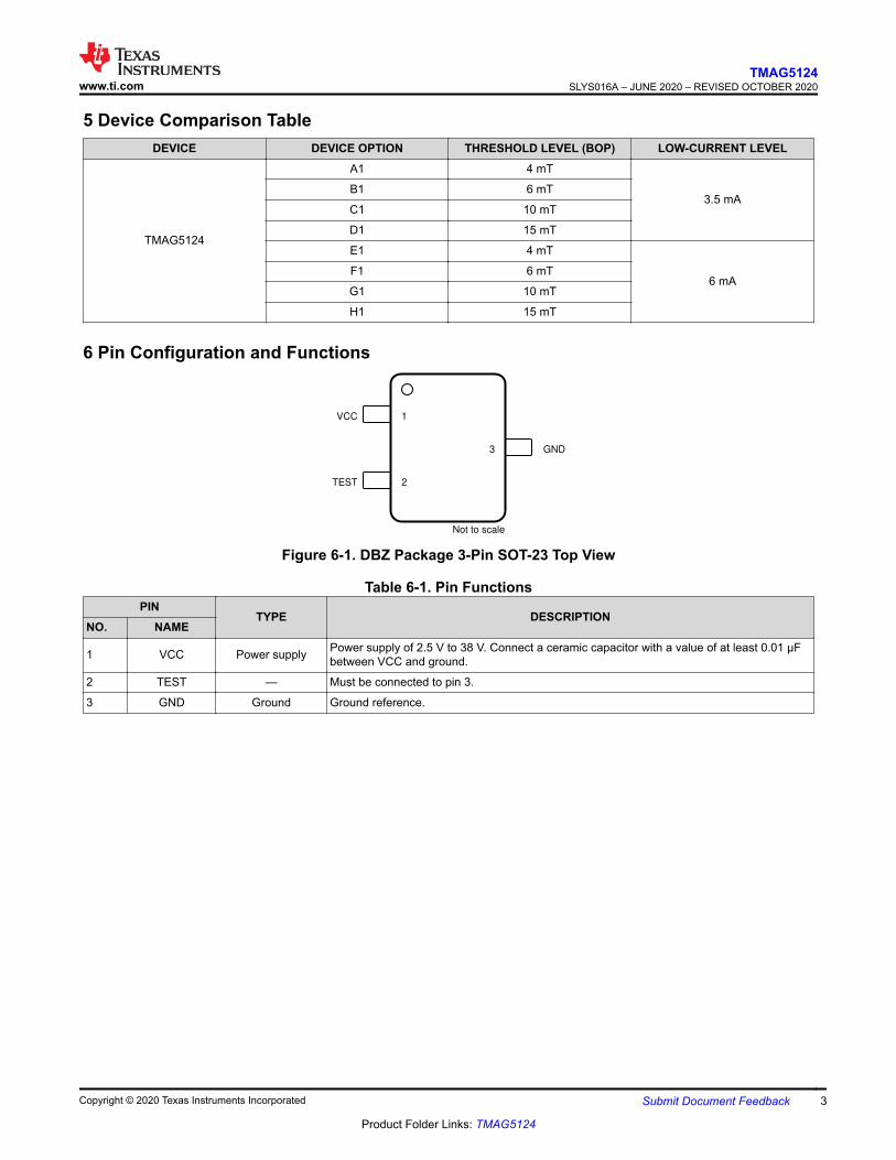
6 Pin Configuration and Functions
1VCC
2TEST
3 GND
Not to scale
Figure 6-1. DBZ Package 3-Pin SOT-23 Top View
Table 6-1. Pin FunctionsPIN
TYPE DESCRIPTIONNO. NAME
1 VCC Power supply Power supply of 2.5 V to 38 V. Connect a ceramic capacitor with a value of at least 0.01 µFbetween VCC and ground.
2 TEST — Must be connected to pin 3.
3 GND Ground Ground reference.
www.ti.comTMAG5124
SLYS016A – JUNE 2020 – REVISED OCTOBER 2020
Copyright © 2020 Texas Instruments Incorporated Submit Document Feedback 3
Product Folder Links: TMAG5124

7 Specifications7.1 Absolute Maximum Ratingsover operating free-air temperature range (unless otherwise noted)(1)
MIN MAX UNITPower SupplyVoltage VCC –20 40 V
Magnetic Flux Density, BMAX Unlimited T
Junctiontemperature TJ 150 °C
Storage temperature, Tstg –65 150 °C
(1) Stresses beyond those listed under Absolute Maximum Rating may cause permanent damage to the device. These are stress ratingsonly, which do not imply functional operation of the device at these or any other conditions beyond those indicated underRecommended Operating Condition. Exposure to absolute-maximum-rated conditions for extended periods may affect devicereliability.
7.2 ESD RatingsVALUE UNIT
V(ESD) Electrostatic discharge
Human body model (HBM), per ANSI/ESDA/JEDEC JS-001, all pins(1) ±2000
VCharged device model (CDM), per JEDECspecificationJESD22-C101, all pins(2) ± 500
(1) JEDEC document JEP155 states that 500-V HBM allows safe manufacturing with a standard ESD control process.(2) JEDEC document JEP157 states that 250-V CDM allows safe manufacturing with a standard ESD control process.
7.3 Recommended Operating Conditionsover operating free-air temperature range (unless otherwise noted)
MIN MAX UNITVCC Power supply voltage 2.5 38 V
TA Ambient temperature –40 125 °C
7.4 Thermal Information
THERMAL METRIC(1)
TMAG5124UNITDBV (SOT-23)
3 PINSRθJA Junction-to-ambient thermal resistance 198.5
°C/W
RθJC(top) Junction-to-case (top) thermal resistance 88.9
RθJB Junction-to-board thermal resistance 28
ΨJT Junction-to-top characterization parameter 4
ΨJB Junction-to-board characterization parameter 27.7
RθJC(bot) Junction-to-case (bottom) thermal resistance — °C/W
(1) For more information about traditional and new thermal metrics, see the Semiconductor and IC Package Thermal Metrics applicationreport.
TMAG5124SLYS016A – JUNE 2020 – REVISED OCTOBER 2020 www.ti.com
4 Submit Document Feedback Copyright © 2020 Texas Instruments Incorporated
Product Folder Links: TMAG5124

7.5 Electrical Characteristicsover operating free-air temperature range (unless otherwise noted)
PARAMETER TEST CONDITIONS MIN TYP MAX UNITPOWER SUPPLY
ICC(L1) Low-level supply current option 1 VCC = 2.5 V to 38 V, TA = – 40 °C to 125°C 2 3.5 5
mAICC(L2) Low-level supply current option 2 VCC = 2.5 V to 38 V, TA = – 40 °C to 125°C 5 6 7.3
ICC(H) High-level supply current VCC = 2.5 V to 38 V, TA = – 40 °C to 125°C 12 14.5 17
IRCC Reverse supply current VRCC = –20 V –100 µA
tON Power-on-time 62.5 µs
OUTPUT
dI/dt Supply Current Slew Rate VCC = 12V, ICC(L) to ICC(H), ICC(H) to ICC(L),CBYP = 0.01µF 10 mA/µs
tPD Propagation delay time Change in B field to change in output 12.5 µs
FREQUENCY RESPONSEfCHOP Chopping frequency 320
kHzfBW Signal bandwidth 40
7.6 Magnetic Characteristicsover operating free-air temperature range (unless otherwise noted)
PARAMETER TEST CONDITIONS MIN TYP MAX UNITTMAG5124A, TMAG5124EBOP Magnetic field operating point
VCC = 2.5 V to 38 V, TA = – 40 °C to 125 °C
3 4 5
mTBRP Magnetic field release point 1 2 3
BHYS Magnetic hysteresis BOP - BRP 0.6 2 3.4
TMAG5124B, TMAG5124FBOP Magnetic field operating point
VCC = 2.5 V to 38 V, TA = – 40 °C to 125 °C
5 6 7
mTBRP Magnetic field release point 3 4 5
BHYS Magnetic hysteresis BOP - BRP 0.6 2 3.4
TMAG5124C, TMAG5124GBOP Magnetic field operating point
VCC = 2.5 V to 38 V, TA = – 40 °C to 125 °C
8.8 10 11
mTBRP Magnetic field release point 6.8 8 9.4
BHYS Magnetic hysteresis BOP - BRP 0.6 2 3.4
TMAG5124D, TMAG5124HBOP Magnetic field operating point
VCC = 2.5 V to 38 V, TA = – 40 °C to 125 °C
13.6 15 16.1
mTBRP Magnetic field release point 11.4 13 14.2
BHYS Magnetic hysteresis BOP - BRP 0.6 2 3.4
www.ti.comTMAG5124
SLYS016A – JUNE 2020 – REVISED OCTOBER 2020
Copyright © 2020 Texas Instruments Incorporated Submit Document Feedback 5
Product Folder Links: TMAG5124

7.7 Typical Characteristics7.7.1 TMAG5124A and TMAG5124E
Ambient Temperature (°C)
Ma
gn
etic F
ield
Op
era
te P
oin
t B
OP
(m
T)
-40 -10 20 50 80 110 1252
3
4
5
6VCC = 3VVCC = 6VVCC = 12V
Figure 7-1. BOP vs TemperatureSupply Voltage (V)
Ma
gn
etic F
ield
Op
era
te P
oin
t B
OP
(m
T)
3 5 7 9 11 122
3
4
5
6TA = -40°CTA = 25°CTA = 125°C
Figure 7-2. BOP vs VCC
Ambient Temperature (°C)
Ma
gn
etic F
ield
Re
lea
se
Po
int
BR
P (
mT
)
-40 -10 20 50 80 110 1251
2
3
4
5VCC = 3VVCC = 6VVCC = 12V
Figure 7-3. BRP vs TemperatureSupply Voltage (V)
Ma
gn
etic F
ield
Re
lea
se
Po
int
BR
P (
mT
)
3 5 7 9 11 121
2
3
4
5TA = -40°CTA = 25°CTA = 125°C
Figure 7-4. BRP vs VCC
Ambient Temperature (°C)
Hyste
resis
(m
T)
-40 -10 20 50 80 110 1250
1
2
3
4VCC = 3VVCC = 6VVCC = 12V
Figure 7-5. Hysteresis vs TemperatureSupply Voltage (V)
Hyste
resis
(m
T)
3 5 7 9 11 120
1
2
3
4TA = -40°CTA = 25°CTA = 125°C
Figure 7-6. Hysteresis vs VCC
TMAG5124SLYS016A – JUNE 2020 – REVISED OCTOBER 2020 www.ti.com
6 Submit Document Feedback Copyright © 2020 Texas Instruments Incorporated
Product Folder Links: TMAG5124

7.7.2 TMAG5124B and TMAG5124F
Ambient Temperature (°C)
Ma
gn
etic F
ield
Op
era
te P
oin
t B
OP
(m
T)
-40 -10 20 50 80 110 1254
5
6
7
8VCC = 3VVCC = 6VVCC = 12V
Figure 7-7. BOP vs TemperatureSupply Voltage (V)
Ma
gn
etic F
ield
Op
era
te P
oin
t B
OP
(m
T)
3 5 7 9 11 124
5
6
7
8TA = -40°CTA = 25°CTA = 125°C
Figure 7-8. BOP vs VCC
Ambient Temperature (°C)
Ma
gn
etic F
ield
Re
lea
se
Po
int
BR
P (
mT
)
-40 -10 20 50 80 110 1252
3
4
5
6VCC = 3VVCC = 6VVCC = 12V
Figure 7-9. BRP vs TemperatureSupply Voltage (V)
Ma
gn
etic F
ield
Re
lea
se
Po
int
BR
P (
mT
)
3 5 7 9 11 122
3
4
5
6TA = -40°CTA = 25°CTA = 125°C
Figure 7-10. BRP vs VCC
Ambient Temperature (°C)
Hyste
resis
(m
T)
-40 -10 20 50 80 110 1250
1
2
3
4VCC = 3VVCC = 6VVCC = 12V
Figure 7-11. Hysteresis vs TemperatureSupply Voltage (V)
Hyste
resis
(m
T)
3 5 7 9 11 120
1
2
3
4TA = -40°CTA = 25°CTA = 125°C
Figure 7-12. Hysteresis vs VCC
www.ti.comTMAG5124
SLYS016A – JUNE 2020 – REVISED OCTOBER 2020
Copyright © 2020 Texas Instruments Incorporated Submit Document Feedback 7
Product Folder Links: TMAG5124

7.7.3 TMAG5124C and TMAG5124G
Ambient Temperature (°C)
Ma
gn
etic F
ield
Op
era
te P
oin
t B
OP
(m
T)
-40 -10 20 50 80 110 1258
9
10
11
12VCC = 3VVCC = 6VVCC = 12V
Figure 7-13. BOP vs TemperatureSupply Voltage (V)
Ma
gn
etic F
ield
Op
era
te P
oin
t B
OP
(m
T)
3 5 7 9 11 128
9
10
11
12TA = -40°CTA = 25°CTA = 125°C
Figure 7-14. BOP vs VCC
Ambient Temperature (°C)
Ma
gn
etic F
ield
Re
lea
se
Po
int
BR
P (
mT
)
-40 -10 20 50 80 110 1256
7
8
9
10VCC = 3VVCC = 6VVCC = 12V
Figure 7-15. BRP vs TemperatureSupply Voltage (V)
Ma
gn
etic F
ield
Re
lea
se
Po
int
BR
P (
mT
)
3 5 7 9 11 126
7
8
9
10TA = -40°CTA = 25°CTA = 125°C
Figure 7-16. BRP vs VCC
Ambient Temperature (°C)
Hyste
resis
(m
T)
-40 -10 20 50 80 110 1250
1
2
3
4VCC = 3VVCC = 6VVCC = 12V
Figure 7-17. Hysteresis vs TemperatureSupply Voltage (V)
Hyste
resis
(m
T)
3 5 7 9 11 120
1
2
3
4TA = -40°CTA = 25°CTA = 125°C
Figure 7-18. Hysteresis vs VCC
TMAG5124SLYS016A – JUNE 2020 – REVISED OCTOBER 2020 www.ti.com
8 Submit Document Feedback Copyright © 2020 Texas Instruments Incorporated
Product Folder Links: TMAG5124

7.7.4 TMAG5124D and TMAG5124H
Ambient Temperature (°C)
Ma
gn
etic F
ield
Op
era
te P
oin
t B
OP
(m
T)
-40 -10 20 50 80 110 12513
14
15
16
17VCC = 3VVCC = 6VVCC = 12V
Figure 7-19. BOP vs Temperature
Supply Voltage (V)
Ma
gn
etic F
ield
Op
era
te P
oin
t B
OP
(m
T)
3 5 7 9 11 1213
14
15
16
17TA = -40°CTA = 25°CTA = 125°C
Figure 7-20. BOP vs VCC
Ambient Temperature (°C)
Ma
gn
etic F
ield
Re
lea
se
Po
int
BR
P (
mT
)
-40 -10 20 50 80 110 12511
12
13
14
15VCC = 3VVCC = 6VVCC = 12V
Figure 7-21. BRP vs TemperatureSupply Voltage (V)
Ma
gn
etic F
ield
Re
lea
se
Po
int
BR
P (
mT
)
3 5 7 9 11 1211
12
13
14
15TA = -40°CTA = 25°CTA = 125°C
Figure 7-22. BRP vs VCC
Ambient Temperature (°C)
Hyste
resis
(m
T)
-40 -10 20 50 80 110 1250
1
2
3
4VCC = 3VVCC = 6VVCC = 12V
Figure 7-23. Hysteresis vs TemperatureSupply Voltage (V)
Hyste
resis
(m
T)
3 5 7 9 11 120
1
2
3
4TA = -40°CTA = 25°CTA = 125°C
Figure 7-24. Hysteresis vs VCC
www.ti.comTMAG5124
SLYS016A – JUNE 2020 – REVISED OCTOBER 2020
Copyright © 2020 Texas Instruments Incorporated Submit Document Feedback 9
Product Folder Links: TMAG5124

7.7.5 Current Output Level7.7.5.1 Low-Level Current Output for TMAG5124A/B/C/D
Ambient Temperature (°C)
I CC
(L1) (m
A)
-40 -10 20 50 80 110 1251
2
3
4
5VCC = 3VVCC = 6VVCC = 12V
Figure 7-25. ICC(L1) vs TemperatureSupply Voltage (V)
I CC
(L1) (m
A)
3 5 7 9 11 121
2
3
4
5TA = -40°CTA = 25°CTA = 125°C
Figure 7-26. ICC(L1) vs VCC
7.7.5.2 Low-Level Current Output for TMAG5124E/F/G/H
Ambient Temperature (°C)
I CC
(L2) (m
A)
-40 -10 20 50 80 110 1254
5
6
7
8VCC = 3VVCC = 6VVCC = 12V
Figure 7-27. ICC(L2) vs TemperatureSupply Voltage (V)
I CC
(L2) (m
A)
3 5 7 9 11 124
5
6
7
8TA = -40°CTA = 25°CTA = 125°C
Figure 7-28. ICC(L2) vs VCC
7.7.5.3 High-Level Current Output for Every Version
Ambient Temperature (°C)
I CC
(H) (m
A)
-40 -10 20 50 80 110 12513
14
15
16
17VCC = 3VVCC = 12VVCC = 24V
Figure 7-29. ICC(H) vs TemperatureSupply Voltage (V)
I CC
(H) (m
A)
3 5 7 9 11 1213
14
15
16
17TA = -40°CTA = 25°CTA = 125C
Figure 7-30. ICC(H) vs VCC
TMAG5124SLYS016A – JUNE 2020 – REVISED OCTOBER 2020 www.ti.com
10 Submit Document Feedback Copyright © 2020 Texas Instruments Incorporated
Product Folder Links: TMAG5124

8 Detailed Description8.1 OverviewThe TMAG5124 is a magnetic sensor with a current interface, also called 2-wire interface, that indicates whenthe magnetic field threshold has been reached. A specific current level is generated depending on its status. Allversions have a high-current level of 14.5 mA. Version A to D have a low-current level of 3.5 mA while version Eto H have a low-current level of 6 mA.
The field polarity is defined as follows: a south pole near the marked side of the package has a positive magneticfield. A north pole near the marked side of the package has a negative magnetic field.
The unipolar south configuration allows the hall sensor to only respond to a south pole. A strong magnetic fieldof south polarity will cause the device to go into a low-current level (operate point, BOP), and a weaker magneticfield will cause the device to go into a high-current level (release point, BRP). Hysteresis is included in betweenthe operate and release points, so magnetic field noise will not trip the device level accidentally.
Since the device does not have an output, the magnitude of device supply current will indicate if the magneticfield exceeds the threshold or not. A resistor can be placed before the VCC pin or after the GND pin to transformthe current into a voltage that can be read by a microcontroler. More details are provided in Section 9.
8.2 Functional Block Diagram
Output
control
GND
LDOCurrent
configuration
Chopper stabilization
VCC
GND
Z Amp
Threshold
selection
��
Figure 8-1. Block Diagram
8.3 Feature Description8.3.1 Field Direction Definition
The TMAG5124 is sensitive to a south pole near the marked side of the package as shown Figure 8-2.
S
N
B > 0 mTSOT-23 (DBZ)
Figure 8-2. Field Direction Definition
www.ti.comTMAG5124
SLYS016A – JUNE 2020 – REVISED OCTOBER 2020
Copyright © 2020 Texas Instruments Incorporated Submit Document Feedback 11
Product Folder Links: TMAG5124

8.3.2 Device Output
When the device is powered on and no magnetic field is applied, the output stays at ICC(H). If the magnetic fieldincreases above the BOP value, then the output turns to ICC(L). The output will remain at this value until themagnetic field decreases to a field value smaller than the BRP threshold.
The ICC(H) for all TMAG5124x versions is between 12 mA to 17 mA. The ICC(L) option for the TMAG5124A/B/C/Dversions is ICC(L1), which is typically 3.5 mA, while The ICC(L) for the TMAG5124E/F/G/H versions is ICC(L2) and istypically 6 mA.
B
ICC
0 mT BOPBRP
BHYS
ICC (L)
ICC (H)
Figure 8-3. Unipolar Functionality
8.3.3 Protection Circuits
The TMAG5124 device is protected against load dump and reverse polarity conditions.
8.3.3.1 Load Dump Protection
The TMAG5124 device operates at DC VCC conditions up to 38 V nominally, and can additionally withstand VCC= 40 V. No current-limiting series resistor is required for this protection.
8.3.3.2 Reverse Polarity Protection
The TMAG5124 device is protected in the event that the VCC pin and the GND pin are reversed (up to –20 V).
TMAG5124SLYS016A – JUNE 2020 – REVISED OCTOBER 2020 www.ti.com
12 Submit Document Feedback Copyright © 2020 Texas Instruments Incorporated
Product Folder Links: TMAG5124

8.3.4 Power-On Time
Figure 8-4 shows the behavior of the device after the VCC voltage is applied and when the field is below the BOPthreshold. When the minimum value for VCC is reached, the TMAG5124 will take time tON to power up and thentime td to update the output to a high level.
Figure 8-5 shows the behavior of the device after the VCC voltage is applied and when the field is above the BOPthreshold. When the minimum value for VCC is reached, the TMAG5124 will take time tON to power up and thentime td to update the output to a high level.
The output value during tON is unknown in both cases. The output value during td will be set at high.
Output (V)
ICC(H)
tON
t (s)
B (mT)
BOP
t (s)
BRP
td
Output (V)
ICC(L)
ICC(H)
tON
t (s)
B (mT)
BOP
t (s)
BRP
td
ICC(L)
Supply (V)
VCC
t (s)
0V
2.5V
Supply (V)
VCC
t (s)
0V
2.5V
Figure 8-4. Power-On Time When B < BOP
Output (V)
ICC(H)
tON
t (s)
B (mT)
BOP
t (s)
Supply (V)
VCC
t (s)
BRP
td
ICC(L)
0V
2.5V
Figure 8-5. Power-On Time When B > BOP
www.ti.comTMAG5124
SLYS016A – JUNE 2020 – REVISED OCTOBER 2020
Copyright © 2020 Texas Instruments Incorporated Submit Document Feedback 13
Product Folder Links: TMAG5124
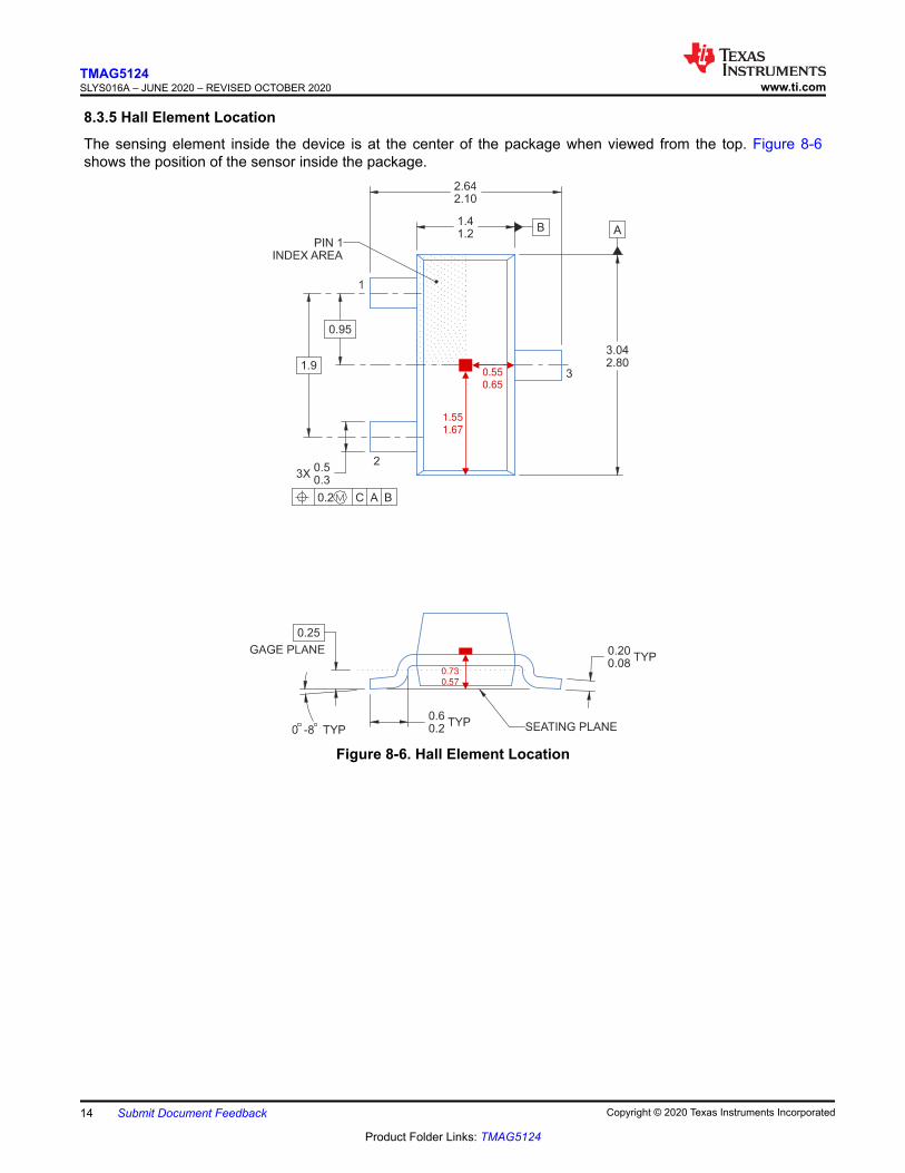
8.3.5 Hall Element Location
The sensing element inside the device is at the center of the package when viewed from the top. Figure 8-6shows the position of the sensor inside the package.
0.55
0.65
1.55
1.67
0.73
0.57
Figure 8-6. Hall Element Location
TMAG5124SLYS016A – JUNE 2020 – REVISED OCTOBER 2020 www.ti.com
14 Submit Document Feedback Copyright © 2020 Texas Instruments Incorporated
Product Folder Links: TMAG5124
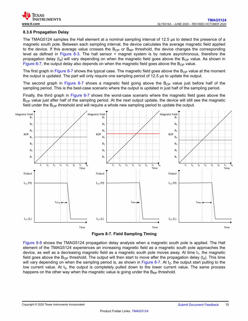
8.3.6 Propagation Delay
The TMAG5124 samples the Hall element at a nominal sampling interval of 12.5 µs to detect the presence of amagnetic south pole. Between each sampling interval, the device calculates the average magnetic field appliedto the device. If this average value crosses the BOP or BRP threshold, the device changes the correspondinglevel as defined in Figure 8-3. The hall sensor + magnet system is by nature asynchronous, therefore thepropagation delay (td) will vary depending on when the magnetic field goes above the BOP value. As shown inFigure 8-7, the output delay also depends on when the magnetic field goes above the BOP value.
The first graph in Figure 8-7 shows the typical case. The magnetic field goes above the BOP value at the momentthe output is updated. The part will only require one sampling period of 12.5 µs to update the output.
The second graph in Figure 8-7 shows a magnetic field going above the BOP value just before half of thesampling period. This is the best-case scenario where the output is updated in just half of the sampling period.
Finally, the third graph in Figure 8-7 shows the worst-case scenario where the magnetic field goes above theBOP value just after half of the sampling period. At the next output update, the device will still see the magneticfield under the BOP threshold and will require a whole new sampling period to update the output.
BOP
Magnetic Field
Output
ICC (L)
ICC (H)
B1
B6
B4
B3
B5
B2
B7
t1 t3t2 t4 t5 t6 t7 t8
BOP
Magnetic Field
Output
ICC (L)
ICC (H)
B1
B6
B4
B3
B5
B2
B7
t1 t3t2 t4 t5 t6 t7 t8
BOP
Magnetic Field
Output
ICC (L)
ICC (H)
B1
B6
B4
B3
B5
B2
B7
t1 t3t2 t4 t5 t6 t7 t8
Time
tdTyp tdMin tdMax
TimeTimeTime
Time Time
Figure 8-7. Field Sampling Timing
Figure 8-8 shows the TMAG5124 propagation delay analysis when a magnetic south pole is applied. The Hallelement of the TMAG5124 experiences an increasing magnetic field as a magnetic south pole approaches thedevice, as well as a decreasing magnetic field as a magnetic south pole moves away. At time t1, the magneticfield goes above the BOP threshold. The output will then start to move after the propagation delay (td). This timewill vary depending on when the sampling period is, as shown in Figure 8-7. At t2, the output start pulling to thelow current value. At t3, the output is completely pulled down to the lower current value. The same processhappens on the other way when the magnetic value is going under the BRP threshold.
www.ti.comTMAG5124
SLYS016A – JUNE 2020 – REVISED OCTOBER 2020
Copyright © 2020 Texas Instruments Incorporated Submit Document Feedback 15
Product Folder Links: TMAG5124

BRP
BOP
Magnetic Field
Time
Time
Output
td
tF
td
tR
ICC (L)
ICC (H)
t1 t2 t3 t4 t5 t6
Figure 8-8. Propagation Delay
8.3.7 Chopper Stabilization
The Basic Hall-effect sensor consists of four terminals where a current is injected through two opposite terminalsand a voltage is measured through the other opposite terminals. The voltage measured is proportional to thecurrent injected and the magnetic field measured. By knowing the current inject, the device can then know themagnetic field strength. The problem is that the voltage generated is small in amplitude while the offset voltagegenerated is more significant. To create a precise sensor, the offset voltage must be minimized.
Chopper stabilization is one way to significantly minimize this offset. It is achieved by "spinning" the sensor andsequentially applying the bias current and measuring the voltage for each pair of terminals. This means that ameasurement is completed once the spinning cycle is completed. The full cycle is completed after fourmeasurements. The output of the sensor is connected to an amplifier and an integrator that will accumulate andfilter out a voltage proportional to the magnetic field present. Finally, a comparator will switch the output if thevoltage reaches either the BOP or BRP threshold (depending on which state the output voltage was previouslyin).
The frequency of each individual measurement is referred as the Chopping frequency, or fCHOP. The totalconversion time is referred as the Propagation delay time, tPD, and is basically equal to 4/fCHOP. Finally, theSignal bandwidth, fBW, represents the maximum value of the magnetic field frequency, and is equal to (fCHOP/4)/2as defined by the sampling theorem.
8.4 Device Functional ModesThe device operates in only one mode when operated within the Recommended Operating Conditions.
TMAG5124SLYS016A – JUNE 2020 – REVISED OCTOBER 2020 www.ti.com
16 Submit Document Feedback Copyright © 2020 Texas Instruments Incorporated
Product Folder Links: TMAG5124

9 Application and ImplementationNote
Information in the following applications sections is not part of the TI component specification, and TIdoes not warrant its accuracy or completeness. TI’s customers are responsible for determiningsuitability of components for their purposes. Customers should validate and test their designimplementation to confirm system functionality.
9.1 Application InformationThe TMAG5124 is typically used in magnetic-field sensing applications to detect the proximity of a magnet. Themagnet is often attached to a movable component in the system.
The TMAG5124 is a Hall sensor that uses current as the signal of interest. Unlike voltage signals, current signalsare much more robust for common problems voltages face in electrical systems, such as voltage sourcefluctuations and source impedance. A major factor that often leads to the choice of a current signal device isimmunity to loop impedance, meaning the signal is capable of being transmitted long distances with ease. Toaccomplish this, the device requires a termination resistor at the end of the path for interfacing the reconstructedvoltage to an input, such as a comparator. Also, diagnostic tools are easily implemented, as disconnects in theloop are easily detected due to a lack of signal.
9.2 Typical Applications9.2.1 High-Side and Low-Side Typical Application Diagrams
C1
0.1 �F
Vcc
GND
TMAG5124
ECU
TEST
VCC GND
VSENSE
Figure 9-1. Typical High-Side Sensing Diagram
TMAG5124
GND
C1
0.1 �F
VccECU
VCC GND
TEST
VSENSE
RSENSE
220
Figure 9-2. Typical Low-Side Sensing Diagram
www.ti.comTMAG5124
SLYS016A – JUNE 2020 – REVISED OCTOBER 2020
Copyright © 2020 Texas Instruments Incorporated Submit Document Feedback 17
Product Folder Links: TMAG5124

9.2.1.1 Design Requirements
For this design example, use the parameters listed in Table 9-1.
Table 9-1. Design ParametersDESIGN PARAMETER EXAMPLE VALUE
VCC 12 V
TMAG5124 Device TMAG5124A1
Magnet 1-cm Cube NdFeB (N45)
Minimum magnet distance 3 cm
Magnetic flux density at closest distance 5.0 mT
Magnetic flux density when magnet moves away Close to 0 mT
9.2.1.2 Detailed Design Procedure
When designing a digital-switch magnetic sensing system, three variables should always be considered: themagnet, sensing distance, and threshold of the sensor.
The TMAG5124 device has a detection threshold specified by parameter BOP, which is the amount of magneticflux required to pass through the Hall sensor mounted inside the TMAG5124. To reliably activate the sensor, themagnet must apply a flux greater than the maximum specified BOP. In such a system, the sensor typicallydetects the magnet before it has moved to the closest position, but designing to the maximum parameterensures robust turn-on for all possible values of BOP. When the magnet moves away from the sensor, it mustapply less than the minimum specified BRP to reliably release the sensor.
Magnets are made from various ferromagnetic materials that have tradeoffs in cost, drift with temperature,absolute maximum temperature ratings, remanence or residual induction (Br), and coercivity (Hc). The Br and thedimensions of a magnet determine the magnetic flux density (B) it produces in 3-dimensional space. For simplemagnet shapes, such as rectangular blocks and cylinders, there are simple equations that solve B at a givendistance centered with the magnet.
Distance
Diameter
Thickness
BS N
Thickness
Distance
BLength
Width
NS
Figure 9-3. Rectangular Block and Cylinder Magnets
Use Equation 1 for the rectangular block shown in Figure 9-3:
� � � �r
2 2 2 2 2 2
B WL WLB arctan arctan
2D 4D W L 2 D T 4 D T W L
§ ·§ ·§ ·¨ ¸¨ ¸ �¨ ¸¨ ¸¨ ¸¨ ¸S ¨ ¸� �¨ ¸© ¹ � � � �© ¹© ¹
:
(1)
TMAG5124SLYS016A – JUNE 2020 – REVISED OCTOBER 2020 www.ti.com
18 Submit Document Feedback Copyright © 2020 Texas Instruments Incorporated
Product Folder Links: TMAG5124

Use Equation 2 for the cylinder shown in Figure 9-3:
� � � � � �r
2 2 2 2
B D T DB
20.5C D T 0.5C D
§ ·�¨ ¸ �¨ ¸
¨ ¸� � �© ¹
:
(2)
where
• W is width.• L is length.• T is thickness (the direction of magnetization).• D is distance.• C is diameter.
The Hall Effect Switch Magnetic Field Calculator is an online tool that uses these formulas available here: http://www.ti.com/product/tmag5124.
All magnetic materials generally have a lower Br at higher temperatures. Systems should have margin toaccount for this, as well as for mechanical tolerances.
For the TMAG5124A1, the maximum BOP is 5 mT. When choosing a 1-cm cube NdFeB N45 magnet, Equation 1shows that this point occurs at 3 cm. This means that the magnet will activate the sensor if the design places themagnet within 3 cm from the sensor during a "turn-on" event. If the magnet is pulled away from the device, themagnetic field will go below the minimum BRP point and the device will return to its initial state.
9.2.1.3 Application Curve
Distance (cm)
Magnetic F
lux D
ensity (
mT
)
1 1.5 2 2.5 3 3.5 4 4.5 50
5
10
15
20
25
30
35
40
45
50
55
60
D017
Figure 9-4. Magnetic Profile of a 1-cm Cube NdFeB Magnet
www.ti.comTMAG5124
SLYS016A – JUNE 2020 – REVISED OCTOBER 2020
Copyright © 2020 Texas Instruments Incorporated Submit Document Feedback 19
Product Folder Links: TMAG5124

10 Power Supply RecommendationsThe TMAG5124 is powered from a DC power supply of 2.5 V to 38 V. A decoupling capacitor close to the devicemust be used to provide local energy with minimal inductance. TI recommends using a ceramic capacitor with avalue of at least 0.01 µF.
10.1 Power DeratingThe device is specified from –40 °C to 125 °C for a voltage rating of 2.5 V to 38 V. The part drains at itsmaximum current of 17 mA, therefore the maximum voltage that can be applied to the device will depend onwhat maximum ambient temperature is acceptable for the application. The curve in Figure 10-1 shows themaximum acceptable power supply voltage versus the maximum acceptable ambient temperature.
Use Equation 3, Equation 4, and Equation 5 to populate the data shown in Figure 10-1:
J AT T T � ' (3)
where
• TJ is the junction temperature.• TA is the ambient temperature.• ΔT is the difference between the junction temperature and the ambient temperature.
D JAT P RT
' u (4)
where
• PD is the power dissipated by the part.• RθJA is the junction to ambient thermal resistance.
D CC CCP = V Iu (5)
where
• VCC is the voltage supply of the device.• ICC is the current consumption of the device.
Combining these equations gives Equation 6, which can be used to determine the maximum voltage the part canhandle in regards of the ambient temperature.
J max ACC max
CC max JA
T TV
I RT
�
u (6)
For example, if an application must work under an ambient temperature maximum of 100 °C, and the TJ max,RθJA and ICC max are the same values defined in the data sheet, then the maximum voltage allowed for thisapplication is calculated in Equation 7:
CC max
150 C 100 CV 14.82 V
17 mA 198.5 C / W
q � q
u q (7)
TMAG5124SLYS016A – JUNE 2020 – REVISED OCTOBER 2020 www.ti.com
20 Submit Document Feedback Copyright © 2020 Texas Instruments Incorporated
Product Folder Links: TMAG5124

Ambient Temperature (°C)
VC
C (
V)
0 20 40 60 80 100 120 140
5
10
15
20
25
30
35
40
Figure 10-1. Power Derating Curve
11 Layout11.1 Layout GuidelinesThe bypass capacitor should be placed near the TMAG5124 to reduce noise. The TEST pin must be connecteddirectly to the GND pin. It is good practice to connect the pins under the package to reduce the connectionlength.
Generally, using PCB copper planes underneath the TMAG5124 device has no effect on magnetic flux and doesnot interfere with device performance. This is because copper is not a ferromagnetic material. However, if nearbysystem components contain iron or nickel, they may redirect magnetic flux in unpredictable ways.
11.2 Layout Example
VCC
GND
TEST
Figure 11-1. TMAG5124 Layout Example
www.ti.comTMAG5124
SLYS016A – JUNE 2020 – REVISED OCTOBER 2020
Copyright © 2020 Texas Instruments Incorporated Submit Document Feedback 21
Product Folder Links: TMAG5124

12 Device and Documentation Support12.1 Documentation Support12.2 Receiving Notification of Documentation UpdatesTo receive notification of documentation updates, navigate to the device product folder on ti.com. Click onSubscribe to updates to register and receive a weekly digest of any product information that has changed. Forchange details, review the revision history included in any revised document.
12.3 Support ResourcesTI E2E™ support forums are an engineer's go-to source for fast, verified answers and design help — straightfrom the experts. Search existing answers or ask your own question to get the quick design help you need.
Linked content is provided "AS IS" by the respective contributors. They do not constitute TI specifications and donot necessarily reflect TI's views; see TI's Terms of Use.
12.4 TrademarksTI E2E™ is a trademark of Texas Instruments.All other trademarks are the property of their respective owners.12.5 Electrostatic Discharge Caution
This integrated circuit can be damaged by ESD. Texas Instruments recommends that all integrated circuits be handledwith appropriate precautions. Failure to observe proper handling and installation procedures can cause damage.ESD damage can range from subtle performance degradation to complete device failure. Precision integrated circuits maybe more susceptible to damage because very small parametric changes could cause the device not to meet its publishedspecifications.
12.6 GlossaryTI Glossary This glossary lists and explains terms, acronyms, and definitions.
13 Mechanical, Packaging, and Orderable InformationThe following pages include mechanical, packaging, and orderable information. This information is the mostcurrent data available for the designated devices. This data is subject to change without notice and revision ofthis document. For browser-based versions of this data sheet, refer to the left-hand navigation.
TMAG5124SLYS016A – JUNE 2020 – REVISED OCTOBER 2020 www.ti.com
22 Submit Document Feedback Copyright © 2020 Texas Instruments Incorporated
Product Folder Links: TMAG5124

PACKAGE OPTION ADDENDUM
www.ti.com 10-Dec-2020
Addendum-Page 1
PACKAGING INFORMATION
Orderable Device Status(1)
Package Type PackageDrawing
Pins PackageQty
Eco Plan(2)
Lead finish/Ball material
(6)
MSL Peak Temp(3)
Op Temp (°C) Device Marking(4/5)
Samples
TMAG5124A1CQDBZR ACTIVE SOT-23 DBZ 3 3000 RoHS & Green SN Level-3-260C-168 HR -40 to 125 4A1
TMAG5124A1CQDBZT ACTIVE SOT-23 DBZ 3 250 RoHS & Green SN Level-3-260C-168 HR -40 to 125 4A1
TMAG5124B1CQDBZR ACTIVE SOT-23 DBZ 3 3000 RoHS & Green SN Level-3-260C-168 HR -40 to 125 4B1
TMAG5124B1CQDBZT ACTIVE SOT-23 DBZ 3 250 RoHS & Green SN Level-3-260C-168 HR -40 to 125 4B1
TMAG5124C1CQDBZR ACTIVE SOT-23 DBZ 3 3000 RoHS & Green SN Level-3-260C-168 HR -40 to 125 4C1
TMAG5124C1CQDBZT ACTIVE SOT-23 DBZ 3 250 RoHS & Green SN Level-3-260C-168 HR -40 to 125 4C1
TMAG5124D1CQDBZR ACTIVE SOT-23 DBZ 3 3000 RoHS & Green SN Level-3-260C-168 HR -40 to 125 4D1
TMAG5124D1CQDBZT ACTIVE SOT-23 DBZ 3 250 RoHS & Green SN Level-3-260C-168 HR -40 to 125 4D1
TMAG5124E1CQDBZR ACTIVE SOT-23 DBZ 3 3000 RoHS & Green SN Level-3-260C-168 HR -40 to 125 4E1
TMAG5124E1CQDBZT ACTIVE SOT-23 DBZ 3 250 RoHS & Green SN Level-3-260C-168 HR -40 to 125 4E1
TMAG5124F1CQDBZR ACTIVE SOT-23 DBZ 3 3000 RoHS & Green SN Level-3-260C-168 HR -40 to 125 4F1
TMAG5124F1CQDBZT ACTIVE SOT-23 DBZ 3 250 RoHS & Green SN Level-3-260C-168 HR -40 to 125 4F1
TMAG5124G1CQDBZR ACTIVE SOT-23 DBZ 3 3000 RoHS & Green SN Level-3-260C-168 HR -40 to 125 4G1
TMAG5124G1CQDBZT ACTIVE SOT-23 DBZ 3 250 RoHS & Green SN Level-3-260C-168 HR -40 to 125 4G1
TMAG5124H1CQDBZR ACTIVE SOT-23 DBZ 3 3000 RoHS & Green SN Level-3-260C-168 HR -40 to 125 4H1
TMAG5124H1CQDBZT ACTIVE SOT-23 DBZ 3 250 RoHS & Green SN Level-3-260C-168 HR -40 to 125 4H1
(1) The marketing status values are defined as follows:ACTIVE: Product device recommended for new designs.LIFEBUY: TI has announced that the device will be discontinued, and a lifetime-buy period is in effect.NRND: Not recommended for new designs. Device is in production to support existing customers, but TI does not recommend using this part in a new design.PREVIEW: Device has been announced but is not in production. Samples may or may not be available.OBSOLETE: TI has discontinued the production of the device.
PACKAGE OPTION ADDENDUM
www.ti.com 10-Dec-2020
Addendum-Page 2
(2) RoHS: TI defines "RoHS" to mean semiconductor products that are compliant with the current EU RoHS requirements for all 10 RoHS substances, including the requirement that RoHS substancedo not exceed 0.1% by weight in homogeneous materials. Where designed to be soldered at high temperatures, "RoHS" products are suitable for use in specified lead-free processes. TI mayreference these types of products as "Pb-Free".RoHS Exempt: TI defines "RoHS Exempt" to mean products that contain lead but are compliant with EU RoHS pursuant to a specific EU RoHS exemption.Green: TI defines "Green" to mean the content of Chlorine (Cl) and Bromine (Br) based flame retardants meet JS709B low halogen requirements of <=1000ppm threshold. Antimony trioxide basedflame retardants must also meet the <=1000ppm threshold requirement.
(3) MSL, Peak Temp. - The Moisture Sensitivity Level rating according to the JEDEC industry standard classifications, and peak solder temperature.
(4) There may be additional marking, which relates to the logo, the lot trace code information, or the environmental category on the device.
(5) Multiple Device Markings will be inside parentheses. Only one Device Marking contained in parentheses and separated by a "~" will appear on a device. If a line is indented then it is a continuationof the previous line and the two combined represent the entire Device Marking for that device.
(6) Lead finish/Ball material - Orderable Devices may have multiple material finish options. Finish options are separated by a vertical ruled line. Lead finish/Ball material values may wrap to twolines if the finish value exceeds the maximum column width.
Important Information and Disclaimer:The information provided on this page represents TI's knowledge and belief as of the date that it is provided. TI bases its knowledge and belief on informationprovided by third parties, and makes no representation or warranty as to the accuracy of such information. Efforts are underway to better integrate information from third parties. TI has taken andcontinues to take reasonable steps to provide representative and accurate information but may not have conducted destructive testing or chemical analysis on incoming materials and chemicals.TI and TI suppliers consider certain information to be proprietary, and thus CAS numbers and other limited information may not be available for release.
In no event shall TI's liability arising out of such information exceed the total purchase price of the TI part(s) at issue in this document sold by TI to Customer on an annual basis.
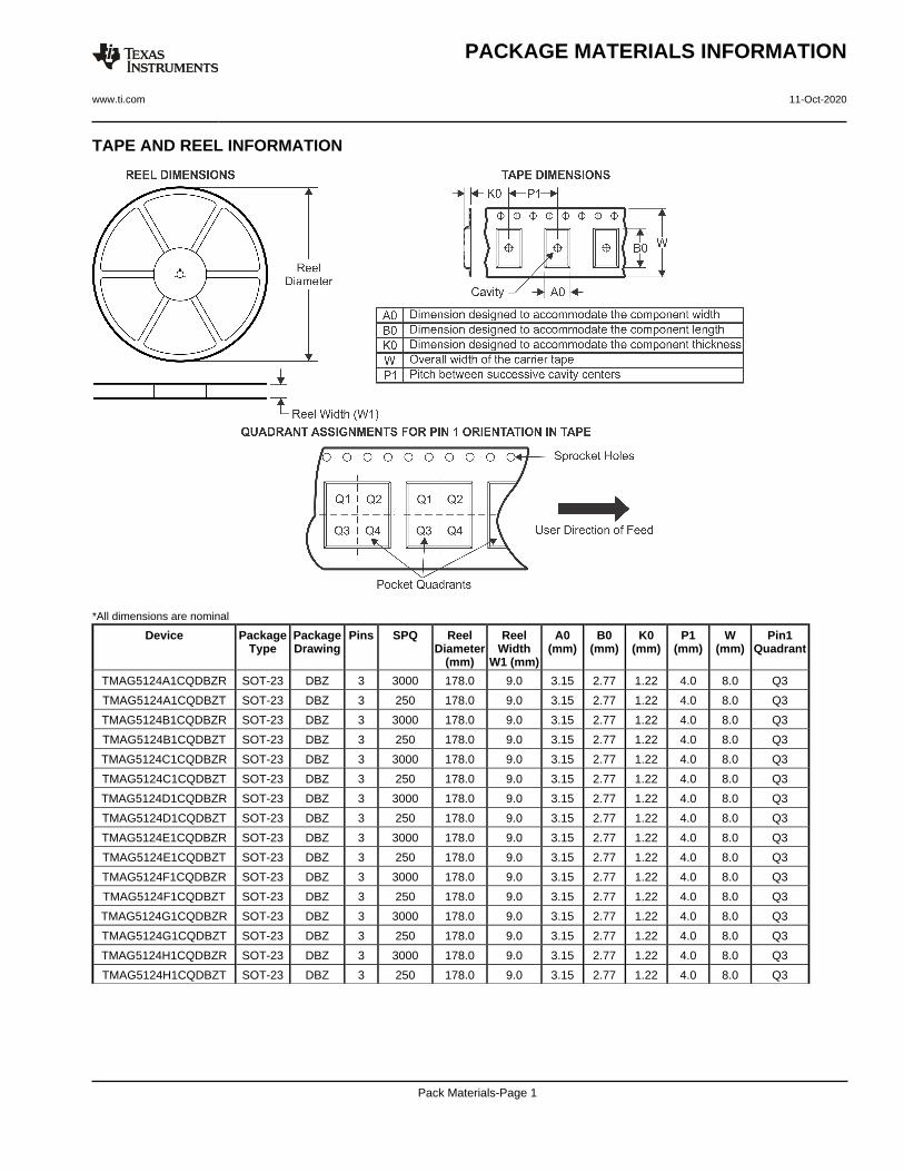
TAPE AND REEL INFORMATION
*All dimensions are nominal
Device PackageType
PackageDrawing
Pins SPQ ReelDiameter
(mm)
ReelWidth
W1 (mm)
A0(mm)
B0(mm)
K0(mm)
P1(mm)
W(mm)
Pin1Quadrant
TMAG5124A1CQDBZR SOT-23 DBZ 3 3000 178.0 9.0 3.15 2.77 1.22 4.0 8.0 Q3
TMAG5124A1CQDBZT SOT-23 DBZ 3 250 178.0 9.0 3.15 2.77 1.22 4.0 8.0 Q3
TMAG5124B1CQDBZR SOT-23 DBZ 3 3000 178.0 9.0 3.15 2.77 1.22 4.0 8.0 Q3
TMAG5124B1CQDBZT SOT-23 DBZ 3 250 178.0 9.0 3.15 2.77 1.22 4.0 8.0 Q3
TMAG5124C1CQDBZR SOT-23 DBZ 3 3000 178.0 9.0 3.15 2.77 1.22 4.0 8.0 Q3
TMAG5124C1CQDBZT SOT-23 DBZ 3 250 178.0 9.0 3.15 2.77 1.22 4.0 8.0 Q3
TMAG5124D1CQDBZR SOT-23 DBZ 3 3000 178.0 9.0 3.15 2.77 1.22 4.0 8.0 Q3
TMAG5124D1CQDBZT SOT-23 DBZ 3 250 178.0 9.0 3.15 2.77 1.22 4.0 8.0 Q3
TMAG5124E1CQDBZR SOT-23 DBZ 3 3000 178.0 9.0 3.15 2.77 1.22 4.0 8.0 Q3
TMAG5124E1CQDBZT SOT-23 DBZ 3 250 178.0 9.0 3.15 2.77 1.22 4.0 8.0 Q3
TMAG5124F1CQDBZR SOT-23 DBZ 3 3000 178.0 9.0 3.15 2.77 1.22 4.0 8.0 Q3
TMAG5124F1CQDBZT SOT-23 DBZ 3 250 178.0 9.0 3.15 2.77 1.22 4.0 8.0 Q3
TMAG5124G1CQDBZR SOT-23 DBZ 3 3000 178.0 9.0 3.15 2.77 1.22 4.0 8.0 Q3
TMAG5124G1CQDBZT SOT-23 DBZ 3 250 178.0 9.0 3.15 2.77 1.22 4.0 8.0 Q3
TMAG5124H1CQDBZR SOT-23 DBZ 3 3000 178.0 9.0 3.15 2.77 1.22 4.0 8.0 Q3
TMAG5124H1CQDBZT SOT-23 DBZ 3 250 178.0 9.0 3.15 2.77 1.22 4.0 8.0 Q3
PACKAGE MATERIALS INFORMATION
www.ti.com 11-Oct-2020
Pack Materials-Page 1
*All dimensions are nominal
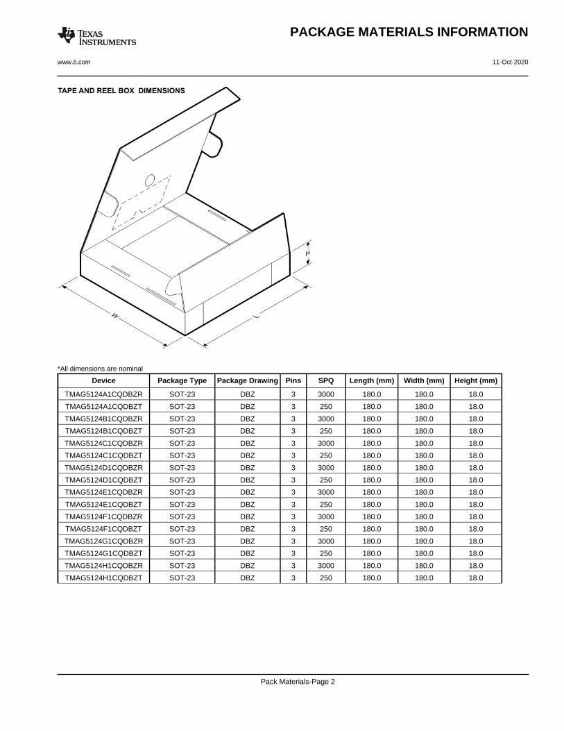
Device Package Type Package Drawing Pins SPQ Length (mm) Width (mm) Height (mm)
TMAG5124A1CQDBZR SOT-23 DBZ 3 3000 180.0 180.0 18.0
TMAG5124A1CQDBZT SOT-23 DBZ 3 250 180.0 180.0 18.0
TMAG5124B1CQDBZR SOT-23 DBZ 3 3000 180.0 180.0 18.0
TMAG5124B1CQDBZT SOT-23 DBZ 3 250 180.0 180.0 18.0
TMAG5124C1CQDBZR SOT-23 DBZ 3 3000 180.0 180.0 18.0
TMAG5124C1CQDBZT SOT-23 DBZ 3 250 180.0 180.0 18.0
TMAG5124D1CQDBZR SOT-23 DBZ 3 3000 180.0 180.0 18.0
TMAG5124D1CQDBZT SOT-23 DBZ 3 250 180.0 180.0 18.0
TMAG5124E1CQDBZR SOT-23 DBZ 3 3000 180.0 180.0 18.0
TMAG5124E1CQDBZT SOT-23 DBZ 3 250 180.0 180.0 18.0
TMAG5124F1CQDBZR SOT-23 DBZ 3 3000 180.0 180.0 18.0
TMAG5124F1CQDBZT SOT-23 DBZ 3 250 180.0 180.0 18.0
TMAG5124G1CQDBZR SOT-23 DBZ 3 3000 180.0 180.0 18.0
TMAG5124G1CQDBZT SOT-23 DBZ 3 250 180.0 180.0 18.0
TMAG5124H1CQDBZR SOT-23 DBZ 3 3000 180.0 180.0 18.0
TMAG5124H1CQDBZT SOT-23 DBZ 3 250 180.0 180.0 18.0
PACKAGE MATERIALS INFORMATION
www.ti.com 11-Oct-2020
Pack Materials-Page 2

4203227/C

www.ti.com
PACKAGE OUTLINE
C
TYP0.200.08
0.25
2.642.10
1.12 MAX
TYP0.100.01
3X 0.50.3
TYP0.60.2
1.9
0.95
TYP-80
A
3.042.80
B1.41.2
(0.95)
SOT-23 - 1.12 mm max heightDBZ0003ASMALL OUTLINE TRANSISTOR
4214838/C 04/2017
NOTES: 1. All linear dimensions are in millimeters. Any dimensions in parenthesis are for reference only. Dimensioning and tolerancing per ASME Y14.5M.2. This drawing is subject to change without notice.3. Reference JEDEC registration TO-236, except minimum foot length.
0.2 C A B
1
3
2
INDEX AREAPIN 1
GAGE PLANE
SEATING PLANE
0.1 C
SCALE 4.000

www.ti.com
EXAMPLE BOARD LAYOUT
0.07 MAXALL AROUND
0.07 MINALL AROUND
3X (1.3)
3X (0.6)
(2.1)
2X (0.95)
(R0.05) TYP
4214838/C 04/2017
SOT-23 - 1.12 mm max heightDBZ0003ASMALL OUTLINE TRANSISTOR
NOTES: (continued) 4. Publication IPC-7351 may have alternate designs. 5. Solder mask tolerances between and around signal pads can vary based on board fabrication site.
SYMM
LAND PATTERN EXAMPLESCALE:15X
PKG
1
3
2
SOLDER MASKOPENINGMETAL UNDER
SOLDER MASK
SOLDER MASKDEFINED
METALSOLDER MASKOPENING
NON SOLDER MASKDEFINED
(PREFERRED)
SOLDER MASK DETAILS

www.ti.com
EXAMPLE STENCIL DESIGN
(2.1)
2X(0.95)
3X (1.3)
3X (0.6)
(R0.05) TYP
SOT-23 - 1.12 mm max heightDBZ0003ASMALL OUTLINE TRANSISTOR
4214838/C 04/2017
NOTES: (continued) 6. Laser cutting apertures with trapezoidal walls and rounded corners may offer better paste release. IPC-7525 may have alternate design recommendations. 7. Board assembly site may have different recommendations for stencil design.
SOLDER PASTE EXAMPLEBASED ON 0.125 THICK STENCIL
SCALE:15X
SYMM
PKG
1
3
2

IMPORTANT NOTICE AND DISCLAIMER
TI PROVIDES TECHNICAL AND RELIABILITY DATA (INCLUDING DATASHEETS), DESIGN RESOURCES (INCLUDING REFERENCE DESIGNS), APPLICATION OR OTHER DESIGN ADVICE, WEB TOOLS, SAFETY INFORMATION, AND OTHER RESOURCES “AS IS” AND WITH ALL FAULTS, AND DISCLAIMS ALL WARRANTIES, EXPRESS AND IMPLIED, INCLUDING WITHOUT LIMITATION ANY IMPLIED WARRANTIES OF MERCHANTABILITY, FITNESS FOR A PARTICULAR PURPOSE OR NON-INFRINGEMENT OF THIRD PARTY INTELLECTUAL PROPERTY RIGHTS.These resources are intended for skilled developers designing with TI products. You are solely responsible for (1) selecting the appropriate TI products for your application, (2) designing, validating and testing your application, and (3) ensuring your application meets applicable standards, and any other safety, security, or other requirements. These resources are subject to change without notice. TI grants you permission to use these resources only for development of an application that uses the TI products described in the resource. Other reproduction and display of these resources is prohibited. No license is granted to any other TI intellectual property right or to any third party intellectual property right. TI disclaims responsibility for, and you will fully indemnify TI and its representatives against, any claims, damages, costs, losses, and liabilities arising out of your use of these resources.TI’s products are provided subject to TI’s Terms of Sale (www.ti.com/legal/termsofsale.html) or other applicable terms available either on ti.com or provided in conjunction with such TI products. TI’s provision of these resources does not expand or otherwise alter TI’s applicable warranties or warranty disclaimers for TI products.
Mailing Address: Texas Instruments, Post Office Box 655303, Dallas, Texas 75265Copyright © 2020, Texas Instruments Incorporated