tm4000 series e 表1 4 入稿no
TRANSCRIPT

TM4000Plus TM4000 TM4000Plus II TM4000 II
TM4000Plus II TM4000 II
TM4000Plus II TM4000 II
Item Descriptipn
Item Descriptipn
Item Description
Magnifications
Model nameModel No.
5 kV, 10 kV, 15 kV, 20 kV*3
■Specifications
Model nameMain unit (motorized stage)Main unit (manual stage)Diaphragm pump
330 (width)×614 (depth)×547 (height), 54 kg330 (width)×617 (depth)×547 (height), 54 kg144 (width)×270 (depth)×216 (height), 5.5 kg
■Size/weight
■Optional accessories
■Installation conditions
Model nameOSMemory device
Windows® 10(64bit)HDD, DVD-ROM Drive
■Required PC specifications
Camera navigation systemEnergy Dispersive X-ray Spectrometer (EDS)
Tilt & rotation stageMulti Zigzag functionCooling stageSTEM holder
1,200 or greater
330200or greater
614
800 or greater
■Installation layout (Main unit:Motorized stage)
Main unit
Diaphragmpump
Power supplysingle phase AC100-240 V(±10%)50/60 Hz,500 VAGrouding 100 ohm or less
unit : mm
210
Normal/Shadow 1/Shadow 2/TOPOX:40 mm, Y:35 mm80 mm (diameter), 50 mm (thickness)Pre-centered cartridge tungsten filament
Image mode (BSE)Sample stage traverseMaximum sample sizeElectron gun
BSE:Conductor/Standard/ Charge-up reductionSE:Standard/ Charge-up reductionMix: Standard/ Charge-up reduction
Backscattered electronSecondary electronMix(Backscattered electron+ Secondary electron)
Backscattered electron
TM4000Plus II/ TM4000 II Specifications
Room temperatureHumidityPower supply (main unit)
15-30 ℃ (△t=within ±2.5℃/h or less)- 70% RH (no condensation)
Singlep phase AC100-240 V(fluctuations in voltage: ±10%)
High-Sensitivity 4-segment BSE detectorHigh-Sensitivity Low-Vacuum SE detector (UVD)
Signal detection system
High-Sensitivity 4-segment BSE detector
*Another power souce for PC is required.
Item Description
Display
Keyboard
PC
Recommended table size:1,200×800 mm or morewithstand load:100 kg or more
270
144
*This logo is the trademark of Hitachi High-Technologies Corporation throughout the world.
Tabletop Microscope
/global/em/
Specifications in this catalog are subject to change with or without notice, as Hitachi High-Technologies Corporation continues to develop the latest technologies and products for our customers.
Notice: For correct operation, follow the instruction manual when using the instrument.
Copyright (C) Hitachi High-Technologies Corporation 2020 All rights reserved.
For technical consultation before purchase, please contact:[email protected]
HTD-E374 2020.1
Auto image-adjustment function
Auto start, Auto focus, Auto brightness
image data savingImage formatData display
2,560 × 1,920 pixels, 1,280 × 960 pixels, 640 × 480 pixelsBMP, TIFF, JPEG
Turbo molecular pump: 67 L/s x 1 unitDiaphragm pump: 20 L/min x 1 unit
Evacuation system (vacuum pump)
Operation help functions
Safety functions
*1 Defined at photo size of 127 mm×95 mm(4"×5" picture size)*2 Defined at display size of 317 mm×238 mm*3 There is a limit to the focus when using 20 kV
*Please make room for more than 200 mm to the left side of a main unit and put it the closest to the center position of the table.*A table with caster is not suitable to put a main unit of TM4000 Series.*Please put a diaphragm pump under the table.*Periodical maintenance is required for this apparatus.*Powercables, earth terminal and table should be prepared by users.*TM4000 Series is not approved as a medical device.*Dedicated mentors, teachers who received the operation training of the instrument are required at compulsory schools.*It is advisable not to install or relocate the instrument by yourselves.*When relocating the system, please contact in advance the sales department that handles your account or a maintenance service company designated by Hitachi.*Screen shows simulated image.*Windows® is a resistered trademark of U.S.Microsoft Corp. in U.S.A. and other countries.*IntelⓇ is a resistered trademark of Intel Corp. or its affilated companies in the United States and/or other countries.
10x - 100,000x (Photographic magnification*1)25x - 250,000x (Monitor display magnification*2)
Accelerating voltage
Vacuum mode
Image signal
BSE:Standard/ Charge-up reduction
Micron marker, micron value, magnification, date and time, image number and comment, WD (Working Distance), accelerating voltage, vacuum mode, image signal, image mode
Over-current protection function, built-in ELCB
Raster rotation, Magnification presets (3 steps), Image shift (±50 μm @ WD6.0 mm)
SeriesTM4000
Three-dimensional image display/measurement function Hitachi map 3D
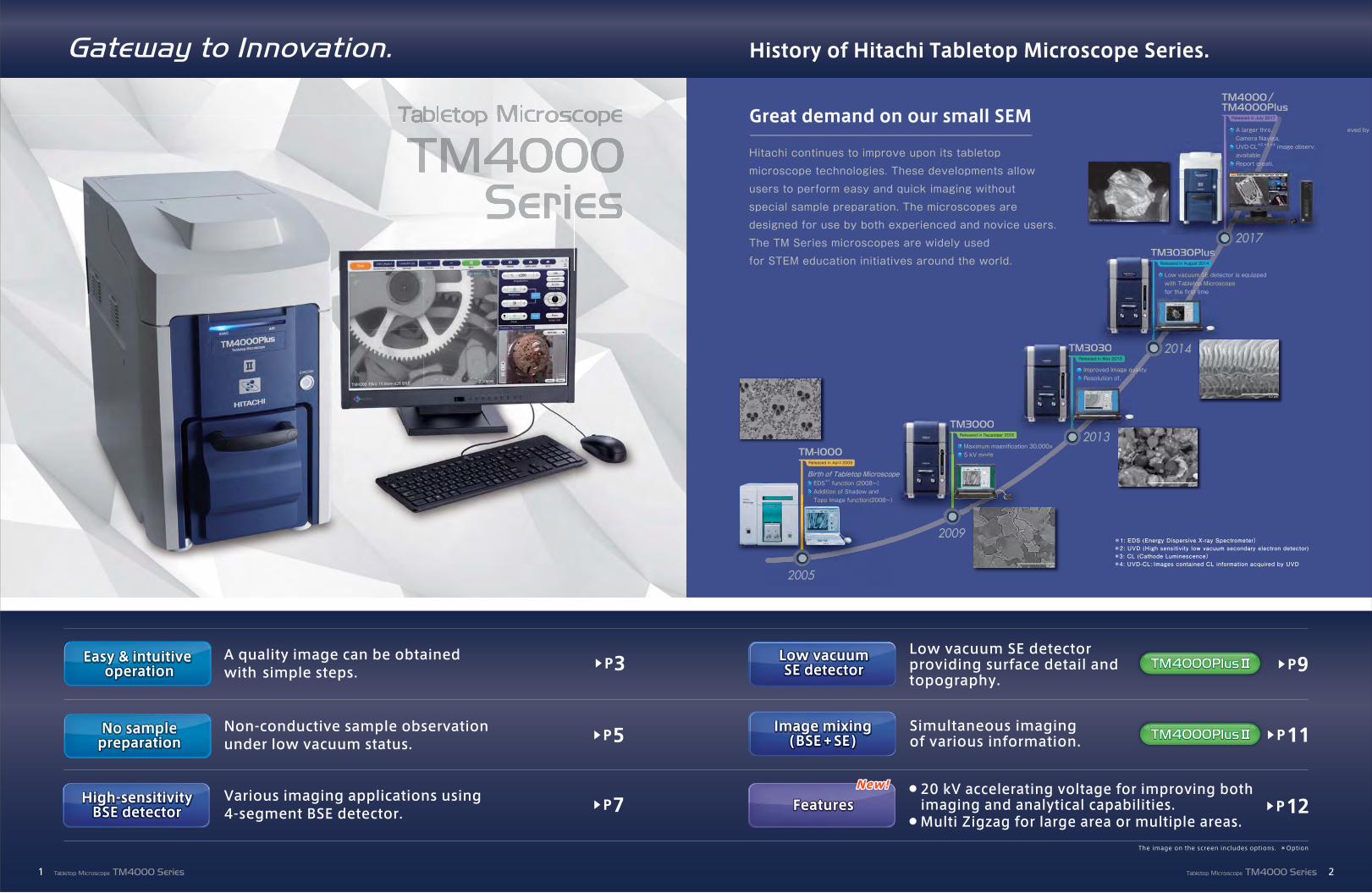
Gateway to Innovation.
Low vacuum SE detector providing surface detail and topography.
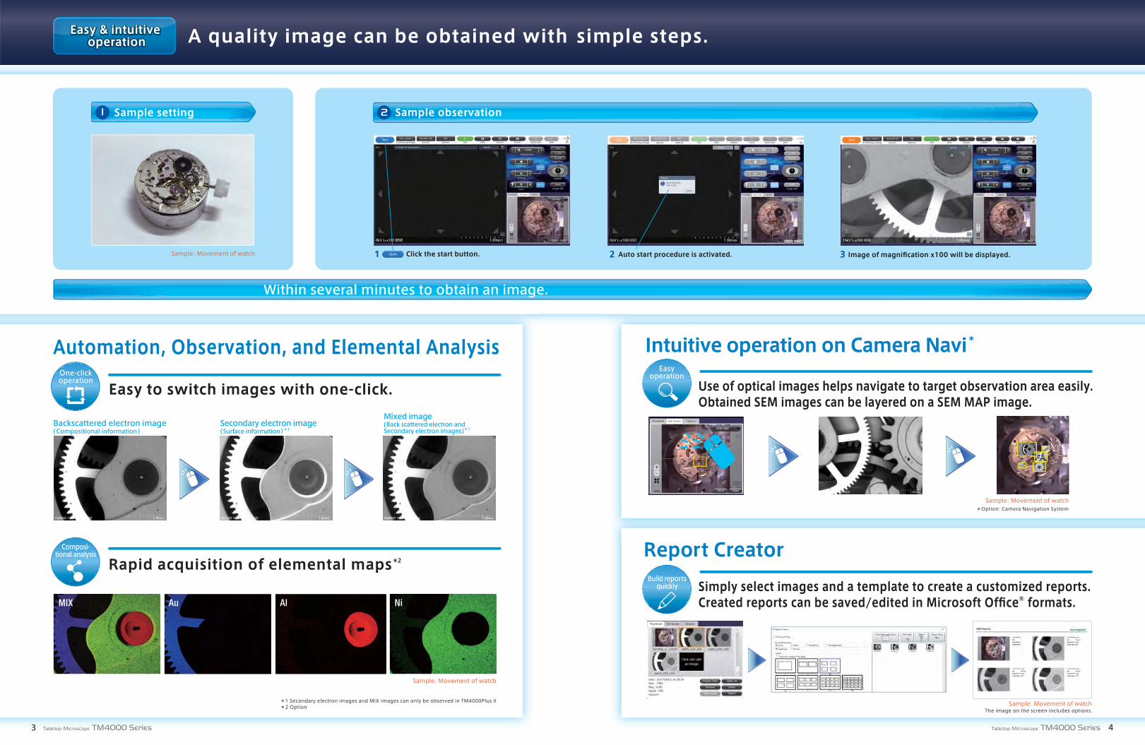
A quality image can be obtained with simple steps.
Non-conductive sample observation under low vacuum status.
Various imaging applications using 4-segment BSE detector.
● 20 kV accelerating voltage for improving both imaging and analytical capabilities.●Multi Zigzag for large area or multiple areas.
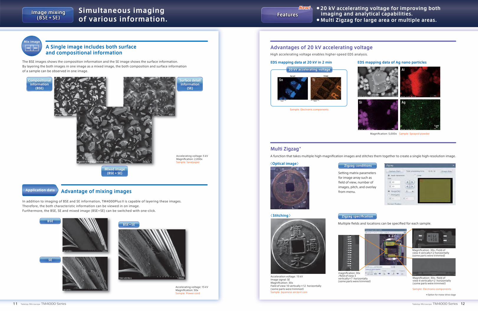
Simultaneous imaging of various information.
▶ P9▶ P3
▶ P5 ▶ P11
▶ P12▶ P7
TTTTTTTTTTTTTTTTTTTTTTTTTTTTTMMMMMMMMMMMMMMMMMMMMMMMMMMMMMMMMMMMMMMMMMMMMM ssuuuuuuusPPPPP000004000 uuuuuulllllllllllPPPPPPPPPPP44444444444 000000000000000000000000000000000 s000000000000000000000000000000000 uuuuuu0000000000000000000000000004 ssssss4444444404040404444444 sssPPPPPPPPPP44444444444 PPPPPP00000000000000000000TM4000Plus
TTTTTTTTTTTTTTTTTTTTTTTTTTTTTMMMMMMMMMMMMMMMMMMMMMMMMMMMMMMMMMMMMMMMMMMMMM susuuuuuusPPPPP000004000 uuuuuulllllllllllPPPPPPPPPPP44444444444 000000000000000000000000000000000 s000000000000000000000000000000000 uuuuuu0000000000000000000000000004 ssssss4444444404040404444444 sssPPPPPPPPPP44444444444 PPPPPP00000000000000000000TM4000Plus
30 µm
20 µm
5.0 µm
Hitachi continues to improve upon its tabletop
microscope technologies. These developments allow
users to perform easy and quick imaging without
special sample preparation. The microscopes are
designed for use by both experienced and novice users.
The TM Series microscopes are widely used
for STEM education initiatives around the world.
EDS*1 function (2008~)Addition of Shadow and Topo image function(2008~)
Birth of Tabletop Microscope
TM-1000Released in April 2005
2005
008~)w and on(2008~~)
Microscopee
Maximum magnification 30,000x 5 kV mode
TM3000Released in December 2009
2009
um magnification 30odeodeode od
00December 2009
0,000x
Improved Image qualityResolution of 5kV is enhanced
TM3030Released in May 2013
2013
Improved I
TM303030Released in May 2
yalityalimage ququa
2013
Low vacuum SE detector is equipped with Tabletop Microscopefor the first time
TM3030PlusReleased in August 2014
2014
TM303TM303Released in A
30Pluss30PlussAugust 2014
A larger throughput is achieved by Camera Navigation System. UVD-CL*2,*3,*4 image observation is available Report creation function
TM4000/TM4000Plus
Released in July 2017
2017
New!New!New!
* 1: EDS (Energy Dispersive X-ray Spectrometer)* 2: UVD (High sensitivity low vacuum secondary electron detector)* 3: CL (Cathode Luminescence)* 4: UVD-CL : Images contained CL information acquired by UVD
The image on the screen includes options. *Option
21
EaEaasysyyyy && iintntnntnttuiuiuiuiuiuitititittivevevvevve opopperereratatat ooionnopopopperereratatioioonn
Easy & intuitive operation
prprprp epepepparararatatatioionnNo samplepreparation
HiHighghgg -s-senensisisissittitittititivvivivivvitytyttytytytyBSBSBSEE ddededetetetectctc ororSBSBSBBSEEE ddettectctororHigh-sensitivityBSE detector
History of Hitachi Tabletop Microscope Series.
Great demand on our small SEM
FeFeFFeatttaturuuruureesesesFeatures
LoLoww vavaccuumumummummumSESESES dddd tetetececttotorrLow vacuumSE detector
ImImagaggee mmixixixxixingngngngngngng(((((BSBSBSBBSBSBSBSEE++SSSEE)))))
Image mixing(BSE+SE)
3 4
Sample: Movement of watch
Easy to switch images with one-click.
Composi-tional analysis
Rapid acquisition of elemental maps*2
Sample: Movement of watch
Sample: Movement of watch
Sample: Movement of watch
Easyoperation
A quality image can be obtained with simple steps.
Sample observationSample setting 1
Within several minutes to obtain an image.
Use of optical images helps navigate to target observation area easily.Obtained SEM images can be layered on a SEM MAP image.
Automation, Observation, and Elemental Analysis Intuitive operation on Camera Navi*
Report Creator
*Option: Camera Navigation System
2 Auto start procedure is activated. 3 Image of magnification x100 will be displayed.
Build reportsquickly Simply select images and a template to create a customized reports.
Created reports can be saved/edited in Microsoft Office® formats.
One-clickoperation
2
Backscattered electron image(Compositional information)
Secondary electron image (Surface information)*1
Mixed image(Back scattered electron and Secondary electron images)*1
AuMIX Al Ni
*1 Secondary electron images and MIX images can only be observed in TM4000Plus II*2 Option
The image on the screen includes options.
1 Click the start button.
Eaasysyyyy &&& iintntnntuiuiuiuuiuittitiitit veevvev oppopperererattat ooionnopopopperere atatioioonn
Easy & intuitive operation

5 6
Non-conductive sample observation under low vacuum status.
Simple observation on water/oil contained samples
Observation without coating
No samplepreparationrequired Charge-up reduction mode
When a non-conductive sample is observed under a high-vacuum state, electrons accumulate on the sample surface causing a charging phenomenon, which prevents imaging. In order to reduce phenomenon, samples are usually coated with a thin layer of conductive material prior to observation. This process is not only time consuming, but also interferes with imaging of surface details as well as EDS analysis. The TM4000 II is equipped “ Charge-up reduction mode” for saving your time and removing the interferes.
Low-vacuum microscopyBy utilizing a lower vacuum level inside the specimen chamber, more gas molecules are present. These gas molecules collide with the electron beam to generate positive ions and electrons . Each positive ion can be neutralized by one of the excess electrons on the specimen surface. This way, the excess electrons on the surface of the sample are removed and the charging is eliminated or reduced.
e G ++ -
Sample: Fracture surface of Resin Sample: Tip of a ball-point penAccelerating voltage:10 kVImage signal:BSE (Shadow) Magnification:150x
Accelerating voltage:5 kV Image signal: SE Magnification:60x
Sample: Recycled paperAccelerating voltage:15 kV Image signal:BSE Magnification:1,000x
Accelerating voltage:15 kV Image signal:BSE Magnification:1,000x
Sample: Leaf of plantSample: Paint inkAccelerating voltage:5 kVImage signal: BSE Magnification: 2,500x
Accelerating voltage:10 kVImage signal: SE Magnification:100x
Chargereduction
Charge on a sample can be reduced by one-click.
Image a variety of materials under low vacuum condition
The images show observations of non-conductive samples such as ink toner particles and a hydrated leaf surface.
Without charge-up reduction mode With charge-up reduction mode
TTTTTTTTTTTTTTTTTTTTTTTTTTTTTMMMMMMMMMMMMMMMMMMMMMMMMMMMMMMMMMMMMMMMMMMMMM sssuuuuuuuuPPPPP000004000 llllllllllluuuuuuPPPPPPPPPPP44444444444 00000000000000000000000000000000000000 0000000000000000000 s000000000000000000000000000000000 uuuuu4000Plussssss4444444404040404444444 sssPPPPPPPPPP44444444444 PPPPPP0000000000000000TM4000PlusTTTTTTTTTTTTTTTTTTTTTTTTTTTTTMMMMMMMMMMMMMMMMMMMMMMMMMMMMMMMMMMMMMMMMMMMMM susuuuuuusPPPPP000004000 llllllllllluuuuuuPPPPPPPPPPP44444444444 000000000000000000000000000000000 s000000000000000000000000000000000 uuuuu4000Plussssss4444444404040404444444 sssPPPPPPPPPP44444444444 PPPPPP0000000000000000TM4000Plus
▶ P7 ▶ P9BSE imageBSE imageBSE image SE imageNon-conductive sample Water/Oil contained sample
Charge-up reduction Mode
Surface &Compositionobservation
NoNo ssamamamplplpplplp eeeeeeprprprp epepepparararatatatioioionnNo samplepreparation
Non-conductivespecimen
Residual gas molecules
eG
+-
BSE Detector
eeGG
++
----- ----
Electron
Positive Ion originated from residual gas molecule
Electron on the surface

7 8
Various imaging applications using 4- segment BSE detector.
Sample: Metal wiringAccelerating voltage: 5 kV Image signal:BSE Magnification: 500x
Sample: Copper crystalAccelerating voltage: 5 kV Image signal:BSE Maghification:3,000x
Compositional contrast and fine structure observationMultiple images observation
Sample: Solder
Accelerating voltage:5 kVImage signal:BSEMaghification:5,000xSample: AlTiC substrate
Multi imageobservation
Three-Dimensional image display/measurement function*
Three-dimensional images are obtainable without sample tilting or concerns about image shift since this 3D function utilizes the 4-segment BSE detector which can detect images from 4 distinct directions.Surface roughness can be measured easily based on the height measurement between 2 points (line profile), and the entire surface area (3D model).
BSE image 3D model
3D model + EDS
3Dfunctionality
Composition/Fine structure
The TM4000 Series is equipped with a high-sensitivity four-segments BSE detector which is used to observe the different brightness levels representing composition in the sample or traditional topographic imaging.
Accelerating voltage:5 kV Image signal:BSE Magnification:3,000x
Sample: Cosmetic foundationAccelerating voltage:15 kV Image signal:BSE Magnification:3,000x
Compositional contrast including surface details using lower accelerating Voltage
5 kV BSE*
Under lower accelerating voltage conditions, the electron signals are generally reduced due to loss of emission and brightness. The TM4000Ⅱ Series optimizes the emission across the voltage range to maintain a higher brightness level, even at the lower 5 kV accelerating voltage.
Sample: Chinese yamAccelerating voltage:15 kV Image signal: BSE Magnification: 400x
Sample: Au Bonding WireSample treated by
Hitachi ion milling system
Accelerating voltage:5 kV Image signal:BSE Magnification: 1,500x
Observation examples using BSE detectorApplication example
Comparison of BSE images between low and high accelerating voltages
■Food (Hydrated sample) ■Electronic components (Grain contrast)
Shadow 2Shadow 1TopoCompo
D B
C
A
D B
C
A
D B
C
A
D B
C
A
The TM4000 II Series features a backscattered-electron detector with four fully controllable independent segments. By utilizing the segments in different combinations, it is possible to emphasize compositional or topographical detail from the sample, as well as producing ‘shadowed’ images which highlight the surface from multiple directions.
*Option
*BSE(Backscattered Electron)
HiHighghgg -s-senene siss ttitittititivvivivvvitytytytyttytyBSBSBSEE ddededetetetectctc ororSBSBSBBSEEE ddettectctororHigh-sensitivityBSE detector

9 10
Low vacuum SE detector providing sur face detail and topography.
Fine surface structure observationApplication data
High-sensitivity Low vacuum SE Detector (UVD)Hitachi’s UVD generates secondary-electron images by detecting visible light excited by the electron gas interactions.
Innovative secondary-electron detector to obtain surface detail with non-conductive samples at lower vacuum conditions
SE imaging underLow vacuum mode
The TM4000Plus II can observe not only conductive samples, but also non-conductive or hydrated samples without sample preparation. Switching between BSE and SE can be performed easily.
SE image (surface information) BSE image compotional information
Sample: Printed paperAccelerating voltage: 5 kV Image signal: BSE Magnification: 800x
Accelerating voltage:5 kV Image signal: SE Magnification: 800x
Sample:DiatomAccelerating voltage:10 kV Image signal: SE Magnification: 10,000x
Sample: Metal fracture surfaceAccelerating voltage: 15 kV Image signal: SE Magnification: 3,000x
Sample: Powder MedicineAccelerating voltage:5 kV Image signal: SE Magnification: 150x
Sample: Functional FilmAccelerating voltage: 5 kV Image signal: SE Magnification: 1,000x
UVD-CL* image observationApplication data
UVD enables to obtain CL information instead of cathode luminescence (CL) detector.In addition, simultaneous imaging of BSE and UVD-CL becomes possible.
Sample: Diamond RingAccelerating voltage:10 kV Image signal: UVD-CL Magnification: 60x
Accelerating voltage: 10 kV Image signal: BSE Magnification: 60x
*UVD-CL: Image contains CL information captured by UVD
Residual gas molecules
Sample
Backscattered electron detector
High sensitivity low vacuum detector
Bias electrode
HV
Amplification in ambient gas
Bias
H
plification Ampn ambient gasin a
Exciting light
Object lens Incident electrons
Positive ions
Electrons
Secondary electronsBackscattered electrons
LoLoww vvacuuuucuumumumummmumSESESEE dddetetetecececectototorrLow vacuumSE detector
1 1 12
Simultaneous imaging of various information.
● 20 kV accelerating voltage for improving both imaging and analytical capabilities.● Multi Zigzag for large area or multiple areas.
New!New!New!
BSEBSE+SE
Zigzag conditions
20 kV accelerating voltage
SE
A Single image includes both surface and compositional information
Advantages of 20 kV accelerating voltageMix image
High accelerating voltage enables higher-speed EDS analysis.
Multi Zigzag*
A function that takes multiple high-magnification images and stitches them together to create a single high-resolution image.
Setting matrix parameters for image array such as field of view, number of images, pitch, and overlay from menu.
Zigzag specification
Multiple fields and locations can be specified for each sample.
In addition to imaging of BSE and SE information, TM4000PlusⅡ is capable of layering these images.Therefore, the both characteristic information can be viewed in on image.Furthermore, the BSE, SE and mixed image (BSE + SE) can be switched with one-click.
The BSE images shows the composition information and the SE image shows the surface information. By layering the both images in one image as a mixed image, the both composition and surface information of a sample can be observed in one image.
Advantage of mixing imagesApplication data
Accelerating voltage: 5 kV Magnification: 2,000xSample: Sandpaper
Sample: Electronic components
Magnification: 5,000x Sample: Sprayed powder
Acceleration voltage: 15 kV Image signal: SEMagnification: 30xField of view 10 vertically×12 horizontally(some parts were trimmed) Sample: Japanese ancient coin
magnification: 30x/field of view 3 vertically×7 horizontally (some parts were trimmed)
Magnification: 30x /field of view 4 vertically×2 horizontally (some parts were trimmed)
Magnification: 30x /Field of view 4 verically×2 horizontally(some parts were trimmed)
Accelerating voltage: 15 kVMagnification: 50xSample: Power cord
Compositionalinformation(BSE)
Mixed image(BSE + SE)
Surface detailinformation (SE)
*Option for motor drive stage
EDS mapping data at 20 kV in 2 min
〈Optical image〉
〈Stitching〉
EDS mapping data of Ag nano particles
Sn Ti
Si
Al
Ag
1 μm
FeFeFeatatttatururuuureeseesesFeatures
Sample: Electronic components
ImImagagggee mimimimimmixixixixxingngngngnggng))))
Image mixing(BSE+SE)

1 3 14
Various EDS for elemental analysis.
Quantax 75
Element
Sample configuration in combination with a TM4000 series instrument
High-energy resolution detector
Advanced EDS features for tabletop SEM
・ Easy to Interpret Data・ Multi user logins・ User configurable windows・ Customizable reporting・ Simplified automation・ Fast mapping・ Collect/Review simultaneously・ Spectrum Match Libraries
Peak fitting function
Si3N4 Window
APEX Software
Live deconvolution to separate overlapping elements
Allows spectra with overlapping peaks to be separated and visually mapped in real time.
High energy resolution detector and advanced user friendly analysis software.
Produced by Bruker nano GmbH
High X-ray transmittance Extreme low energy detection Hexagonal support grid for increased transmission
■Si ■■W
Si
W
Si
W
Automatic background subtraction and peak fitting (automatic/arbitrary) provide highly reliable element identification. To be able to estimate the self-measurement conditions, electron beam penetration depth, spread, and density in the actual sample, it is possible to simulate the actual measurement area.
Produced by EDAX Inc.
Al L(72 eV ) spectrum example
Aztec Series
Live EDS spectrum
Mapping Image
Live Spectrum View is available on the TM4000 User Interface to see the X-ray spectrum with Automatically labelled peaks. It allows you to confirm elemental information with secondary electron images and/or backscattered electron images, even while moving around your sample.
Live EDSfunction
The TruMap feature allows multi-element spectra to be properly separated and background subtracted in real time, resulting in a precise elemental map with no image contamination due to overlapping peaks.
High precision/ Highly reliableTruMap
The AZtecEnergy system offers advanced analytical functionality and flexible configurations with an ability to automate analysis via a motorized stage. AztecEnergy enables large-area mapping and particle analysis.
Advanced Analysis Functions
Mg K (1.26 keV) As L (1.30 keV) Mg K (1.26 keV) As L (1.30 keV)
Typical ROI MAP
TruMap
Sample : Sulfide ore
7 view segments
(2.2 mm)
The mapping software automatically acquires data for multiple specified regions to produce a single combined set of mapping information.
AZtecLiveOne
e AZtecEnergy
Large-area mapping
Produced byOxford Instruments NanoAnalysis
AZtecLiveOne: standard feature AZtecOne: Option
・ Live Spectrum Viewer with Automatically labelled peaks can be shown. (AZtecLiveOne)
・ High-throughput analysis with high-precision pile-up correction function and TruQTM Technologies.
・ TruMap generates element maps that peak overlaps removed in real time.
EDEDEDEDSSSSSS opoopopopptititioonoononsssEDS options
The high-energy resolution detector allows light elements such as boron to be analyzed with high accuracy.
Sample configuration in combination with a TM4000 series instrument
Sample configuration in combination with a TM4000 series instrument
48 view segments (17.6 mm)Magnifications: 400x
Sample: Cross section of electronic component
Si3N4 Window to optimize low energy X-ray transmission for light element analysis. Compared with conventional detector window, there is improved mapping speed and detection limit.
Accelerating voltage: 10 kVMeasurement time: 90 sec
Si3N4 windowPolymer window

15 16
*Option
StStSttSttagagggaggeee OpOOOpOOpptittitioonononsssStage Options
Image Processing, Measurement, and Analysis Software: Image Pro® for Hitachi
Accelerating voltage: 10 kV Image signal: MixMagnification: 200x Sample: Petal
The TM4000Ⅱ features integration icon to transfer images into Image Pro® Software with a single click.
Cooling stage
The cooling stage allows samples to be cooled to temperatures as low as -25 ℃ and kept at the temperature up to a few hours. It is particularly well suited for observation of hydrated samples such as foods and biological tissues, or samples susceptible to thermal damage.
Tilt: 0°
Tilt: 45°+Rotation
Tilt: 45°+Rotation
Selection of stages.Software for image post-processing.Easy maintenance.
Particle size and distribution analysis example Capable to transfer images from SEM software
Transfer button
Temperaturecontrol 20
0
10
20
Tilt & Rotation stage
Observation range of 15° to 60° tilting angles and full 360° rotation are available on the tilt and rotation stage.
Stagecontrol
Oil-free vacuum pump and pre centered cartridge filaments are equipped a standard.
Maintenance kit available for your daily use.*
Easy maintenance
Diaphragm pumpPre-centered cartridge filament
Self Support
Produced by Deben UK Ltd. Produced by Media Cybernetics
Produced by Deben UK Ltd.
Accelerating voltage: 15 kV Image signal: BSE, Mix Magnification: 150xSample: Haemphysalis longicornis Sample courtesy of professor Tomoyuki Shimano, Hosei University
LowtemperatureObservation
Roomtemperatureobservation
Binary automaticmeasurement
画像の繋ぎ合わせ
30
20
10
0
-10
-20
-30
-40
-50
-606 10 102 103 104
Pressure(Pa)
A water (Ice) vapor pressure curve
Temperature(℃
)
Freezing
Freezing
Evaporation
SSSSooooofffffftttttwwwwwwaaaaaarrrreeee tt ooooppppptttttiooonnSoftware option
Particle Analysis
Fiber measurement
画画Stitching Image
MMMMMaaaaaiiiinnnnnnttttteeeeennnnnaaaanncceeeMaintenance
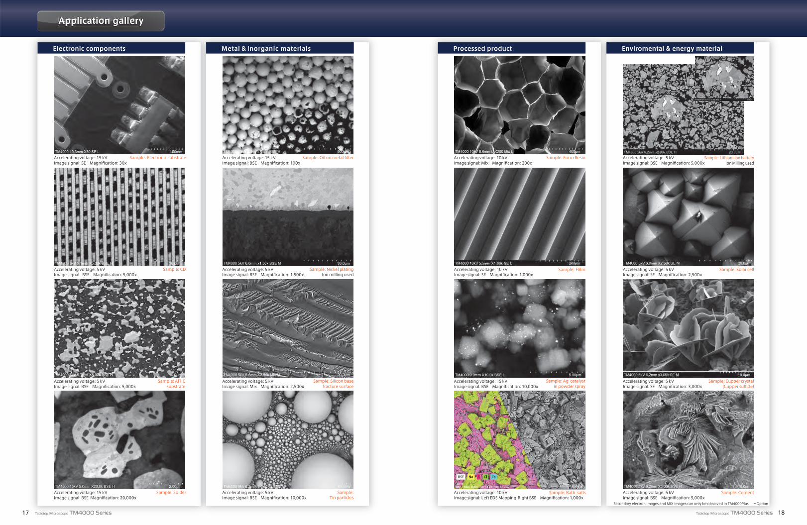
Sample: Form ResinAccelerating voltage: 10 kV Image signal: Mix Magnification: 200x
Sample: FIilmAccelerating voltage: 10 kV Image signal: SE Magnification: 1,000x
Processed product
Sample: Lithium Ion batteryIon Milling used
Accelerating voltage: 5 kV Image signal: BSE Magnification: 5,000x
Sample: Solar cellAccelerating voltage: 5 kV Image signal: SE Magnification: 2,500x
Enviromental & energy material
Sample: Cupper crystal(Cupper sulfide)
Accelerating voltage: 5 kV Image signal: SE Magnification: 3,000x
Sample: Ag catalystin powder spray
Accelerating voltage: 15 kV Image signal: BSE Magnification: 10,000x
Sample: Bath saltsAccelerating voltage: 10 kV Image signal: Left EDS Mapping Right BSE Magnification: 1,000x
Sample: CementAccelerating voltage: 5 kV Image signal: BSE Magnification: 5,000x
17 18
Sample: Electronic substrateAccelerating voltage: 15 kV Image signal: SE Magnification: 30x
Sample: CDAccelerating voltage: 5 kV Image signal: BSE Magnification: 5,000x
Electronic components
Sample: Oil on metal filterAccelerating voltage: 15 kV Image signal: BSE Magnification: 100x
Sample: Silicon basefracture surface
Accelerating voltage: 5 kV Image signal: Mix Magnification: 2,500x
Sample: Nickel platingIon milling used
Accelerating voltage: 5 kV Image signal: BSE Magnification: 1,500x
Metal & inorganic materials
Sample: AlTiCsubstrate
Accelerating voltage: 5 kV Image signal: BSE Magnification: 5,000x
Sample: SolderAccelerating voltage: 15 kV Image signal: BSE Magnification: 20,000x
Sample:Tin particles
Accelerating voltage: 5 kV Image signal: BSE Magnification: 10,000x
Secondary electron images and MIX images can only be observed in TM4000Plus II *Option
AAApppppplicccaaatttiiiooonnn gggaaallllleeryyApplication gallery

19 20
AAAppppppliccaaatttiiiooonnn gggaaallllleeryyApplication gallery
Biology & foodstuffs & MedicineMinerals
Processed product
Sample:Ceder pollen
Sample: Zircon
Sample: fluorescence brightener
Accelerating voltage: 10 kV Image signal: BSE Magnification: 3,000x
Sample: ChocolateCooling stage used
Accelerating voltage: 5 kV Image signal: BSE Magnification: 500x
Sample:Leaf stomata
Accelerating voltage: 10 kV Image signal: BSE Magnification: 1,000x
Sample: tabletAccelerating voltage: 5 kVImage signal: SE Magnification: 200x
Accelerating voltage: 15 kV Magnification: 2,500x
Accelerating voltage: 15 kV Magnification: 2,500x
Sample:Abrasive
Accelerating voltage: 20 kVImage signal: (a) STEM, (b) BSEMagnification: 10,000 x
Sample:Rat kidney
Accelerating voltage: 15 kV Image signal: STEMMagnification: 1,000 x
Sample:Rat liver
Accelerating voltage: 15 kV Image signal: STEMMagnification: 5,000 x
Accelerating voltage: 10 kV Magnification: 400x
Accelerating voltage: 10 kV Magnification: 400x
Zircon UVD-CL*1 observation exampleFollowing are BSE and UVD-CL images of a zircon cross section. Although the compositional difference cannot be confirmed from the BSE image, the UVD-CL image shows the difference via the striped pattern from the emission intensity. This zircon also contains apatite as an inclusion. Zr which is one of the components of “Zircon” and P which is the component of apatite are overlapped in each peak. Normally this combination of elements is difficult to identify with traditional EDS ※2 mapping, but the distribution of Zr and P can be distinguished by using a peak separation mapping.
UVD-CL*1 observaiton for fluorescence brightener on paperDispersion of fluorescence brightener which is used for color development on paper is difficult to distinguish between SE and BSE detectors, but UVD-CL allows for these brightener particles to be visible.
The newly developed STEM holder can be used to perform transmission images with the Hitachi UVD. Images of thin or biological samples can be obtained.
BSE Image
EDS Mapping
UVD-CL Image
BSE Image UVD-CL Image
Zr Si P Ca
Easily obtain transmitted images on thin samplesSTEM Holder
E-beamSample
Scintillator
UVD*
Light
*UVD is a function of TM4000Plus II.
UVD is function of TM4000PlusⅡ *Option
*1 UVD-CL: Image contains CL information captured by UVD *2 Option
(a) (b)

21 22
Workflow approach to asbestos analysis Element specification
Aztec series specification for TM4000 series
Made by EDAX Inc.Quantax75 specification Made by Bruker nano GmbH
Made by Oxford Instruments NanoAnalysis
■DetectorItem AZtecOne AZtecLiveOne AZtecEnergy
Item AZtecOne AZtecLiveOne AZtecEnergy
Item AZtecOne AZtecLiveOne AZtecEnergy
Item AZtecOne AZtecLiveOne AZtecEnergy
Detector TypeDetector AreaEnergy resolutionDetection ElementThermal CycleCooling Method
Silicon drift detector (SDD)30 mm2
158 eV (Cu Ka) (Mn Ka: equivalent of 137 eV)B5~U92Detector cool down on demand2 stage thermoelectric cooling (without fan/LN2 free)
■Software
Item
Live spectrum
Spectrum displayQualitative analysisQuantitative analysisImage acuisitonElement mappping
Line Scan
Point & ID
TruMap
AssistanceData managementReport preparation
Option
Live Spectrum Monitor on Viewer window with automatically labelled peakScaling display in horizontal and vertical directions, KLM markers and/or peak profile displayedAuto / Manual by TruQTM technology, Pulse PileStandard less analysis by XPP correction, 100% normalized2,048×1,536, 1,024×768, 512×3841,024×768, 512×384, 256×192, 128×96, Tiled or Layered viewlayered Image: No limit on the number of X-ray maps that can be overlaid on SEM imageReconstruct Spectrum from mapping during/after acquisitionArbitrary line position and direction may be specified; The colour and thickness of the Linescans for each element may be changed.Linescans can be viewed in a Vertical tiled,Stacked or table of values Spectra can be reconstructed from any point on the linescanAcquire from point, rectangle, ellipse or freehandOverlap a spectrum from any project in the Data Tree over the current spectrum
■Size/weight
DetectorAnalyzer unit
145 (width) × 150 (depth) × 200 (height) mm, 2.7 kg290 (width) × 260 (depth) × 330 (height) mm, 10 kg
Item ■Installation conditions
Power supply Single Phase AC, 100-240 V, 50/60 Hz, 400 VA Single-phase AC, 100-240 V, 50/60 Hz, 1,500 VA
Operation guide functionalityData saved in individual projectsQuick and easy reporting functionality・ Content selectable via radial buttons・ Exports in Microsoft ® Word format (reports can be viewed in free Microsoft viewer)
Detector typeDetector areaEnergy resolution
Detection elementCooling methodEnergy channel
■Detector
Silicon drift detector (SDD)30 mm2
148 eV(Cu-Kα)(Mn-Kα:⦆ equivalent of 129 eV or less)B5~Cf982-stage thermoelectric (peltier) cooling (without fan and LN2 free)4,096 channel (2.5 eV/ch at minimum)
100 (width) × 45 (depth) × 120 (height) mm, 1.45 kg225 (width) × 230 (depth) × 150 (height) mm, 3.65 kg
■Software
Qualitative analysisQuantitative analysisAnalysis mode
Element mapping
Report preparation features
Auto/manualStandardless quantitative analysis, normalized to 100%Object mode (including point, rectangle, ellipse and polygon)Line scanHypermap (mapping, spot analysis, line analysis)Maximum map image resolution 1,600x1,200Rainbow mapOnline deconvolutionTemplates for printing may be preparedPDF, Microsoft® Word, Excel
■Size/weight
DetectorScaning control unit
Item Description
Item Description
Item Description
Single-phase AC, 100/240 V 50/60 Hz
■Installation conditions
Power supplyItem Description
Window typeType of SensorSensor sizeEnergy resolutionDetection rangeCooling system
■Detector
Silicon Nitride WindowsSilicon drift detector (SDD)30 mm2
129 eV (Mn-Kα)Be4~Am95Thermoelectric Peltier cooling (fan and LN free)No cooling required when not in use
169 (width) × 435 (depth) ×356 (height) mm, 12 kg100 (width) × 45 (depth) ×120 (height) mm, 0.5 kg73 (width) × 171 (depth) ×121 (height) mm, 1.6 kg
■Software
Qualitative analysisQuantitative analysisAnalysis mode
X-ray Map
Reporting
Auto/Manual, HPDStandardless Method, Graph view/Statistics displaySpectrum (Point, Area, Free Draw, Grid)Linescan (Spectral Linescan, Review and Rebuild)X-ray Map (Spectral Map, Review and Rebuild)1,024×800 (Max.)Spectral Map (Review Spectrum, Line from Map, Rebuild Map)Comp Map (Real-time Peak deconvalution map)Quant Map (Concentration map)Drift CollectionReport Template for PrintingPDF, Microsoft® Word, Excel, PowerPoint
■Size/weight
PC WorkstationDetectorDPP Box
Item Description
Item Description
Item Description
Single-phase AC100/240 V 50/60 Hz
■Installation conditions
Power supplyItem Description
64 - 8,192 pixels64 - 4,096 pixelslayered Image: No limit on the number of X-ray maps that can be overlaid on SEM image Reconstruct Spectrum from mapping during/after acquisition
Comprehensive list of Report templates that can be exported in Word and Excel formatImage, Maps and Spectra can be saved as selectable image files with user control over resolution and formatTruMap (TruLine), AZtec Large Area Mapping, AZtec Feature, etc,
Overlap and background corrected mapping and LineScanning during/after acquisition
Mics F+ ; 180 (width) × 260 (depth) ×330 (height) mm, 2.6 kgX-stream2: 180 (width) × 260 (depth) ×330 (height) mm, 2.6 kg
EDS specification (option)
Image signal: BSEMagnification: 2,000xSample: Tremolite (asbestos standard sample)
Multiple fields of view can automatically be captured .
Ease of setting matrix parameters
Choose thumbnails with fibers
Confirm aspect ratio and fiber length
Spot analysis for elemental confirmationGet EDS Spectrum*
One click takes you to fiber of interest
Fine tuning for best image quality
*Option
Step1 ▶ Locating fiber on filter
Step2 ▶ confirmation of fiber locations within matrix
Step3 ▶ Measuring the fiber diameter and elemental confirmation
…
20.20.9 μmμm20.9 μm
1.141.14 μmμm1.14 μm
29.29.6 μmμm29.6 μm
55555 nm555 nm
The TM4000Ⅱ Series can count and analyze asbestos fibers by using EDS * along with Multi Zigzag.
-
- -
AAAppppppliccaaatttiiiooonnn gggaaallllleeryyApplication gallery
optional optional
Live Spectrum Monitor on Mini Viewwith automatically labelled peak