tm enhanced rs-232 line...
TRANSCRIPT

�Jan 3�-07 Rev B SP232A/233A/3�0A/3�2A © 2007 Sipex Corporation
SP232A/233A/310A/312A
Available in Lead Free Packaging
Solved by
TM
Enhanced RS-232 Line Drivers/Receivers
■ Operates from Single +5V Power Supply ■ Meets All RS-232F and ITU V.28
Specifications ■ Operates with 0.1µF to 1µF Capacitors ■ High Data Rate – 120Kbps Under Load ■ Low Power CMOS – 3mA Operation (SP232A) ■ No External Capacitors Required (SP233A) ■ Low Power Shutdown (SP310A,SP312A) ■ Enhanced ESD Protection (2kV Human
Body Model)
Number of RS232 No. of Receivers No. of External Model Drivers Receivers Active in Shutdown 0.1µF Capacitors Shutdown WakeUp TTL Tri–State SP232A 2 2 N//A 4 No No NoSP233A 2 2 N/A 0 No No NoSP310A 2 2 0 4 Yes No YesSP312A 2 2 2 4 Yes Yes Yes
DESCRIPTION
SELECTION TABLE
The SP232A/233A/310A/312A devices are a family of line driver and receiver pairs that meet the specifications of RS-232 and V.28 serial protocols. These devices are pin-to-pin compatible with popular industry standards. As with the initial versions, the SP232A/233A/310A/312A devices feature at least 120Kbps data rate under load, 0.1µF charge pump capacitors, and overall ruggedness for commercial applications. This family also features Sipex's BiCMOS design allowing low power operation without sacrificing performance. The series is available in plastic DIP and SOIC packages operating over the commercial and industrial temperature ranges.
Now Available in Lead Free Packaging
VCC
GND
T1OUT
R1IN
R1OUT
T1IN
T2IN
R2OUT
C1+
V+
C1-
C2+
C2-
V-
T2OUT
R2IN
SP
232A
1
2
3
4
5
6
7
8
16
15
14
13
12
11
10
9
FEATURES
2Jan 3�-07 Rev B SP232A/233A/3�0A/3�2A © 2007 Sipex Corporation
This is a stress rating only and functional operation of the device atthese or any other conditions above those indicated in the operationsections of this specification is not implied. Exposure to absolutemaximum rating conditions for extended periods of time may affectreliability.Vcc ................................................................................................................................................................. +6VV+ .................................................................................................................... (Vcc-0.3V) to +11.0VV- ............................................................................................................................................................ -11.0VInput VoltagesTIN ......................................................................................................................... -0.3 to (Vcc +0.3V)RIN ............................................................................................................................................................ ±30V
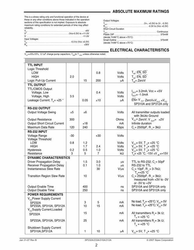
VCC=+5V±10%; 0.1µF charge pump capacitors; TMINto T MAX unless otherwise noted.
PARAMETERS MIN. TYP. MAX. UNITS CONDITIONSTTL INPUTLogic Threshold
LOW 0.8 Volts TIN; EN, SDHIGH 2.0 Volts TIN; EN, SD
Logic Pull-Up Current 15 200 µA TIN= ZeroVTTL OUTPUTTTL/CMOS Output
Voltage, Low 0.4 Volts IOUT= 3.2mA; Vcc = +5VVoltage, High 3.5 Volts IOUT= -1.0mA
Leakage Current; TA= +25 ° 0.05 ±10 µA EN= V CC, ZeroV VOUT VCC SP310A and SP312A only
RS-232 OUTPUTOutput Voltage Swing ±5 ±6 Volts All transmitter outputs loaded
with 3k to GroundOutput Resistance 300 Ohms VCC= ZeroV; V OUT= ±2VOutput Short Circuit Current ±18 mA Infinite durationMaximum Data Rate 120 240 Kbps CL= 2500pF, R L= 3kRS-232 INPUTVoltage Range -30 +30 VoltsVoltage Threshold
LOW 0.8 1.2 Volts VCC= 5V, T A= +25 °CHIGH 1.7 2.4 Volts VCC= 5V, T A= +25 °C
Hysteresis 0.2 0.5 1.0 Volts VCC= 5V, T A= +25 °CResistance 3 5 7 k TA= +25 °C, -15V V IN +15VDYNAMIC CHARACTERISTICSDriver Propagation Delay 1.5 3.0 µs TTL to RS-232; CL= 50pFReceiver Propagation Delay 0.1 1.0 µs RS-232 to TTLInstantaneous Slew Rate 30 V/µs CL= 10pF, R L= 3-7k ;
TA=+25 °CTransition Region Slew Rate 10 V/µs CL= 2500pF, R L= 3k ;
measured from +3V to -3V or -3V to +3V
Output Enable Time 400 ns SP310A and SP312A onlyOutput Disable Time 250 ns SP310A and SP312A onlyPOWER REQUIREMENTSVCCPower Supply Current SP232A 3 5 mA No load, TA= +25°C; VCC= 5V SP233A, SP310A, SP312A 10 15 mA No load, TA= +25°C; VCC= 5VVCCSupply Current,Loaded SP232A 15 mA All transmitters RL= 3k ;
TA = +25 °C SP233A, SP310A, SP312A 25 mA All transmitters RL= 3k ;
TA = +25 °CShutdown Supply Current SP310A,SP312A 1 10 µA VCC= 5V, T A= +25 °C
ELECTRICAL CHARACTERISTICS
ABSOLUTE MAXIMUM RATINGS
Output VoltagesTOUT .................................................................................................... (V+, +0.3V) to (V-, -0.3V)ROUT ................................................................................................................ -0.3V to (Vcc +0.3V)Short Circuit DurationTOUT ......................................................................................................................................... ContinuousPlastic DIP .......................................................................... 375mW(derate 7mW/°C above +70°C)Small Outline ...................................................................... 375mW(derate 7mW/°C above +70°C)
3Jan 3�-07 Rev B SP232A/233A/3�0A/3�2A © 2007 Sipex Corporation
PERFORMANCE CURVES
-55 -40 0 25 70 85 125Temperature (°C)
0
5
10
15
20
25
30
VCC= 6V
VCC= 5V
VCC= 4V
VCC= 3V
I CC
(mA
)
0 5 10 15 20Load Current (mA)
0
6
8
10
12
V+ (V
olts
)
2
4
VCC= 5V
VCC= 4V
VCC= 6V
25 30 35 400 2 4 6 8 10 12 14Load Current (mA)
V– V
olta
ge (V
olts
)
-3
-4
-5
-6
-7
-8
-9
-10
-11
VCC= 6V
VCC= 5V
VCC= 4V
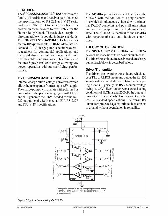
PINOUTS
4.5 4.75 5.0 5.25 5.5VCC(Volts)
5.0
6.5
7.0
7.5
8.0
8.5
9.0
Load current = 0mATA= 25 °CV O
H (V
olts
)
5.5
6.0
VCC
GND
T1OUT
R1IN
R1OUT
T1IN
T2IN
R2OUT
C1+
V+
C1-
C2+
C2-
V-
T2OUT
R2IN
SP
232A
1
2
3
4
5
6
7
8
16
15
14
13
12
11
10
9
R2OUT
R2IN
T2OUT
Conn to 10
Conn to 11
Conn to 12
C1- DNC
C1+ DNC
Conn to 15
Conn to 16
T2IN
T1IN
R1OUT
R1IN
T1OUT
GND
VCC
V+ DNC
GND
Conn to 17
1
2
3
4
5
6
7
8
9
10
20
19
18
17
16
15
14
13
12
11
SP233AC
T/AET
20-PIN SOIC
See Figure 2 for Pin Connections
R OUT
R IN
T OUT
V-
C -
C +
V+
C -
V-
C +
2
1
2
T IN
T IN
R OUT
R IN
T OUT
GND
V
C +
GND
C -
1
2
2
1
2
3
4
5
6
7
8
9
10
20
19
18
17
16
15
14
13
12
11
1
1
1
CC
1
2
2
2
2
SP233AC
P/AEP
20-PIN PLASTIC DIP
ON/OFF
VCC
GND
T1OUT
R1IN
R1OUT
T1IN
T2IN
R2OUT
NC *C1+
V+
C1-
C2+
C2-
V-
T2OUT
R2IN
1
2
3
4
5
6
7
8
9
18
17
16
15
14
13
12
11
10
SP310A
SHUTDOWN
VCC
GND
T1OUT
R1IN
R1OUT
T1IN
T2IN
R2OUT
EN *C1+
V+
C1-
C2+
C2-
V-
T2OUT
R2IN
1
2
3
4
5
6
7
8
9
18
17
16
15
14
13
12
11
10
SP312A
* N.C. for SP310E_A, EN for SP312E_A
Not 100% tested.
�Jan 3�-07 Rev B SP232A/233A/3�0A/3�2A © 2007 Sipex Corporation
Figure 1. Typical Circuit using the SP232A.
FEATURES…The SP232A/233A/310A/312A devices are afamily of line driver and receiver pairs that meetthe specifications of RS-232 and V.28 serialprotocols. The ESD tolerance has been im-proved on these devices to over ±2KV for theHuman Body Model. These devices are pin-to-pin compatible with popular industry standards.The SP232A/233A/310A/312A devicesfeature10V/µs slew rate, 120Kbps data rate un-der load, 0.1µF charge pump capacitors, overallruggedness for commercial applications, andincreased drive current for longer and moreflexible cable configurations. This family alsofeatures Sipex's BiCMOS design allowing lowpower operation without sacrificing perfor-mance.
The SP232A/233A/310A/312A devices haveinternal charge pump voltage converters whichallow them to operate from a single +5V supply.The charge pumps will operate with polarized ornon-polarized capacitors ranging from 0.1 to 1µFand will generate the ±6V needed for the RS-232 output levels. Both meet all EIA RS-232Fand ITU V.28 specifications.
The SP310A provides identical features as theSP232A with the addition of a single controlline which simultaneously shuts down the inter-nal DC/DC converter and puts all transmitterand receiver outputs into a high impedancestate. The SP312A is identical to the SP310Awith separate tri-state and shutdown controllines.
THEORY OF OPERATIONThe SP232A, SP233A, SP310A and SP312Adevices are made up of three basic circuit blocks –1) a driver/transmitter, 2) a receiver and 3) a chargepump. Each block is described below.
Driver/TransmitterThe drivers are inverting transmitters, which ac-cept TTL or CMOS inputs and output the RS-232signals with an inverted sense relative to the inputlogic levels. Typically the RS-232output voltageswing is ±6V. Even under worst case loadingconditions of 3kOhms and 2500pF, the output isguaranteed to be ±5V, which is consistent with theRS-232 standard specifications. The transmitteroutputs are protected against infinite short-circuitsto ground without degradation in reliability.
R29 8 R INR OUT2
R112 13 R INR OUT1
T210 7T IN2 T OUT2
T111 14T IN1 T OUT1
15GND
400k
400k
TTL/
CM
OS
INPU
TS
RS-
232
OU
TPU
TS
3
1C +
C -1
1
6
16V CC
V+
+
+0.1 F6.3Vµ
Charge Pump
+5V INPUT
2
V-
TTL/
CM
OS
OU
TPU
TS
RS-
232
INPU
TS
2
1
5k
0.1 F10Vµ
5k
5
4C +
C -2
2+0.1 F10Vµ
0.1 F 6.3Vµ
10 F 6.3Vµ
SP232A
+
+ *
*The negative terminal of the V+ storage capacitor can be tied to either VCCor GND. Connecting the capacitor to V CC(+5V) is recommended.
�Jan 3�-07 Rev B SP232A/233A/3�0A/3�2A © 2007 Sipex Corporation
The instantaneous slew rate of the transmitteroutput is internally limited to a maximum of 30V/µs in order to meet the standards [EIA RS-232-F ].The transition region slew rate of these enhancedproducts is typically 10V/µs. The smooth transi-tion of the loaded output from VOL to VOH clearlymeets the monotonicity requirements of the stan-dard [EIA RS-232-F].
ReceiversThe receivers convert RS-232 input signals toinverted TTL signals. Since the input is usuallyfrom a transmission line, where long cable lengthsand system interference can degrade the signal, the
inputs have a typical hysteresis margin of 500mV.This ensures that the receiver is virtually immuneto noisy transmission lines.
The input thresholds are 0.8V minimum and 2.4Vmaximum, again well within the ±3V RS-232requirements. The receiver inputs are also pro-tected against voltages up to ±25V. Should aninput be left unconnected, a 5K pulldown resis-tor to ground will commit the output of the receiverto a high state.
Figure 2. Typical Circuits using the SP233ACP and SP233ACT
Figure 3. Typical Circuits using the SP310A and SP312A
R220 19 R INR OUT2
R13 4 R INR OUT1
T21 18T IN2 T OUT2
T12 5T IN1 T OUT1
9
GND
400k
400k
TTL/
CM
OS
INP
UTS
RS
-232
OU
TPU
TS
13
8 C +
C -
V+
V-
V-
1
1
10
7VCC
+5V INPUT
11
TTL/
CM
OS
OU
TPU
TS
RS
-232
INP
UTS
2
1
5k
5k
17
12
C +
C +
C -
C -
2
2
GND
6
14 15
162
2
Do not makeconnection to
these pins
SP233ACP
Connect on PCB
Pin 11 to Pin 15Pin 10 to Pin 16Pin 12 to Pin 17Both Pins 6 and 9 to GND
R220 19 R INR OUT2
R13 4 R INR OUT1
T21 18T IN2 T OUT2
T12 5T IN1 T OUT1
9
GND
400k
400k
TTL/
CM
OS
INP
UTS
RS
-232
OU
TPU
TS
14
13 C +
C -
V+
V-
V-
1
1
11
7VCC
+5V INPUT
12
TTL/
CM
OS
OU
TPU
TS
RS
-232
INP
UTS
2
1
5k
5k
17
10
C +
C +
C -
C -
2
2
GND
6
8 15
162
2
Do not makeconnection to
these pins
SP233ACT
Connect on PCB
Pin 12 to Pin 15Pin 11 to Pin 16Pin 10 to Pin 17Both Pins 6 and 9 to GND
R210 9 R INR OUT2
R113 14 R INR OUT1
T211 8T IN2 T OUT2
T112 15T IN1 T OUT1
16GND
400k
400k
TTL/
CM
OS
INP
UTS
RS
-232
OU
TPU
TS
4
2C +
C -1
1
7
17V CC
V+
+
+0.1 F6.3Vµ
Charge Pump
+5V INPUT
3
V-
TTL/
CM
OS
OU
TPU
TS
RS
-232
INP
UTS
2
1
5k
5k
6
5C +
C -2
2+0.1 F16Vµ
10 F 6.3Vµ
SP310A
+
18 ON/OFF
+
0.1 µF10V
*
*The negative terminal of the V+ storage capacitor can be tied to either VCCor GND. Connecting the capacitor to V CC(+5V) is recommended.
0.1 µF10V
R210 9
R INR OUT2
R113 14
R INR OUT1
T211 8T IN2 T OUT2
T112 15T IN1 T OUT1
16GND
400k
400k
TTL/
CM
OS
INP
UTS
RS
-232
OU
TPU
TS
4
2C +
C -1
1
7
17V CC
V+
+
+0.1 F6.3Vµ
+5V INPUT
3
V-
TTL/
CM
OS
OU
TPU
TS
RS
-232
INP
UTS
2
1
5k
0.1 F10Vµ
5k
6
5C +
C -2
2+0.1 F16Vµ
Charge Pump
10 F 6.3Vµ
SP312A
+
18 SHUTDOWN1EN
+
0.1 F10Vµ
*
*The negative terminal of the V+ storage capacitor can be tied to either VCCor GND. Connecting the capacitor to V CC(+5V) is recommended.
�Jan 3�-07 Rev B SP232A/233A/3�0A/3�2A © 2007 Sipex Corporation
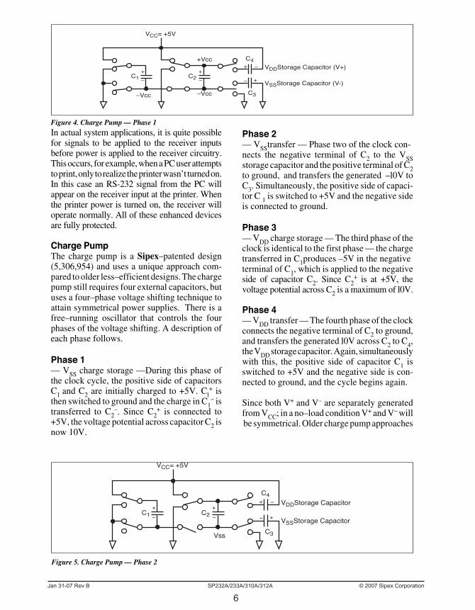
Figure 4. Charge Pump — Phase 1
Figure 5. Charge Pump — Phase 2
In actual system applications, it is quite possiblefor signals to be applied to the receiver inputsbefore power is applied to the receiver circuitry.This occurs, for example, when a PC user attemptsto print, only to realize the printer wasn’t turned on.In this case an RS-232 signal from the PC willappear on the receiver input at the printer. Whenthe printer power is turned on, the receiver willoperate normally. All of these enhanced devicesare fully protected.
Charge PumpThe charge pump is a Sipex–patented design(5,306,954) and uses a unique approach com-pared to older less–efficient designs. The chargepump still requires four external capacitors, butuses a four–phase voltage shifting technique toattain symmetrical power supplies. There is afree–running oscillator that controls the fourphases of the voltage shifting. A description ofeach phase follows.
Phase 1— VSS charge storage —During this phase ofthe clock cycle, the positive side of capacitorsC1 and C2 are initially charged to +5V. Cl
+ isthen switched to ground and the charge in C1
– istransferred to C2
–. Since C2+ is connected to
+5V, the voltage potential across capacitor C2 isnow 10V.
Phase 2— VSStransfer — Phase two of the clock con-nects the negative terminal of C2 to the VSSstorage capacitor and the positive terminal of C2to ground, and transfers the generated –l0V toC3. Simultaneously, the positive side of capaci-tor C 1 is switched to +5V and the negative sideis connected to ground.
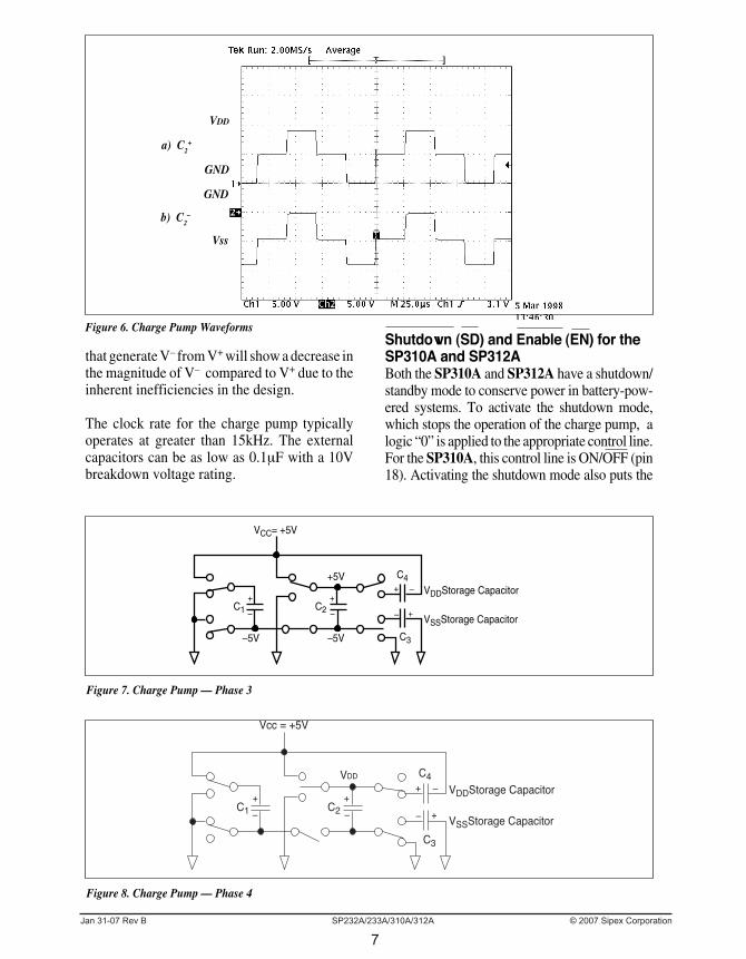
Phase 3— VDD charge storage — The third phase of theclock is identical to the first phase — the chargetransferred in C1produces –5V in the negativeterminal of C1, which is applied to the negativeside of capacitor C2. Since C2
+ is at +5V, thevoltage potential across C2 is a maximum of l0V.
Phase 4— VDD transfer — The fourth phase of the clockconnects the negative terminal of C2 to ground,and transfers the generated l0V across C2 to C4,the VDD storage capacitor. Again, simultaneouslywith this, the positive side of capacitor C1 isswitched to +5V and the negative side is con-nected to ground, and the cycle begins again.
Since both V+ and V– are separately generatedfrom VCC; in a no–load condition V+ and V– will be symmetrical. Older charge pump approaches
VCC= +5V
–Vcc
+Vcc
VSSStorage Capacitor (V-)
VDDStorage Capacitor (V+)C1 C2
C3
C4+
++ +
–
–––
–Vcc
VCC= +5V
Vss
VSSStorage Capacitor
VDDStorage CapacitorC1 C2
C3
C4+
++ +
–
–––
7Jan 3�-07 Rev B SP232A/233A/3�0A/3�2A © 2007 Sipex Corporation
Figure 6. Charge Pump Waveforms
VDD
a) C2+
GND
GND
b) C2–
Vss
Figure 7. Charge Pump — Phase 3
VCC= +5V
–5V
+5V
–5V
VSSStorage Capacitor
VDDStorage Capacitor
C1 C2
C3
C4+
+
+ +–
–––
Figure 8. Charge Pump — Phase 4
that generate V– from V+ will show a decrease inthe magnitude of V– compared to V+ due to theinherent inefficiencies in the design.
The clock rate for the charge pump typicallyoperates at greater than 15kHz. The externalcapacitors can be as low as 0.1µF with a 10Vbreakdown voltage rating.
Shutdown (SD) and Enable (EN) for theSP310A and SP312ABoth the SP310A and SP312A have a shutdown/standby mode to conserve power in battery-pow-ered systems. To activate the shutdown mode,which stops the operation of the charge pump, alogic “0” is applied to the appropriate control line.For the SP310A, this control line is ON/OFF (pin18). Activating the shutdown mode also puts the
Vcc = +5V
VDD
VSSStorage Capacitor
VDDStorage CapacitorC1 C2
C3
C4+
++ +
–
–––
�Jan 3�-07 Rev B SP232A/233A/3�0A/3�2A © 2007 Sipex Corporation
Table 1. Wake-up Function Truth Table.
SP310A transmitter and receiver outputs in a highimpedance condition (tri-stated). The shutdownmode is controlled on the SP312A by a logic “0”on the SHUTDOWN control line (pin 18); this alsoputs the transmitter outputs in a tri–state mode.The receiver outputs can be tri–stated separatelyduring normal operation or shutdown by a logic“1” on the ENABLE line (pin 1).
Wake–Up Feature for the SP312AThe SP312A has a wake–up feature that keepsall the receivers in an enabled state when thedevice is in the shutdown mode. Table 1 definesthe truth table for the wake–up function.
With only the receivers activated, the SP312Atypically draws less than 5µA supply current.In the case of a modem interfaced to a computerin power down mode, the Ring Indicator (RI)signal from the modem would be used to "wakeup" the computer, allowing it to accept datatransmission.
After the ring indicator signal has propagatedthrough the SP312A receiver, it can be used totrigger the power management circuitry of thecomputer to power up the microprocessor, andbring the SD pin of the SP312A to a logic high,taking it out of the shutdown mode. The receiverpropagation delay is typically 1µs. The enabletime for V+ and V– is typically 2ms. After V+ andV– have settled to their final values, a signal canbe sent back to the modem on the data terminalready (DTR) pin signifying that the computer isready to accept and transmit data.
Pin Strapping for the SP233ACT/ACPThe SP233A packaged in the 20–pin SOIC pack-age (SP233ACT) has a slightly different pinoutthan the SP233A in PDIP packaging (SP233ACP).To operate properly, the following pairs of pinsmust be externally wired together:
SD ENPower
Up/DownReceiverOutputs
0011
0101
DownDown
UpUp
EnableTri–stateEnable
Tri–state
Pins Wired Together SOIC PDIP
Two V- Pins 10 & 17 12 & 17Two C2+ Pins 12 & 15 11 & 15Two C2- Pins 11 & 16 10 & 16
No Connections for Pins 8, 13, and 14
Connect Pins 6 and 9 to GND
�Jan 3�-07 Rev B SP232A/233A/3�0A/3�2A © 2007 Sipex Corporation
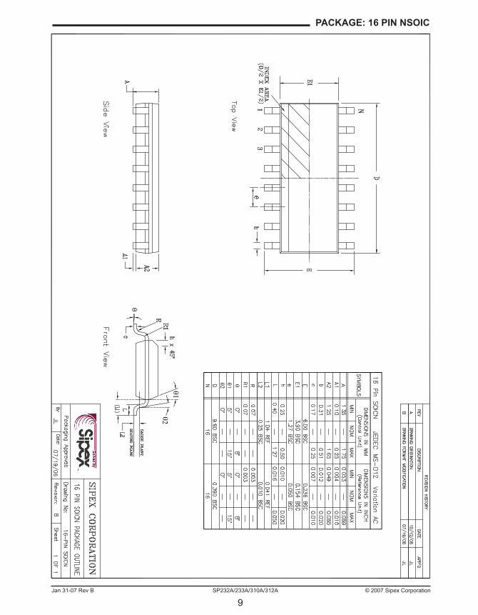
PAckAgE: 16 Pin nSoic
�0Jan 3�-07 Rev B SP232A/233A/3�0A/3�2A © 2007 Sipex Corporation
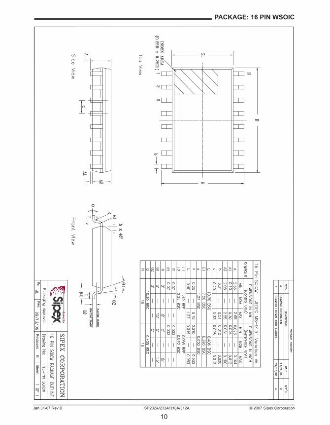
PAckAgE: 16 Pin WSoic
��Jan 3�-07 Rev B SP232A/233A/3�0A/3�2A © 2007 Sipex Corporation
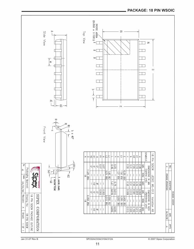
PAckAgE: 18 Pin WSoic
�2Jan 3�-07 Rev B SP232A/233A/3�0A/3�2A © 2007 Sipex Corporation
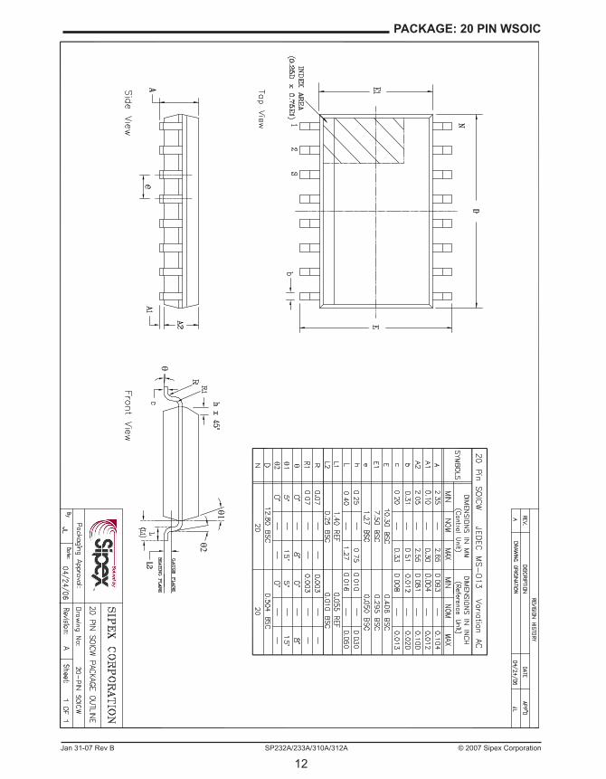
PAckAgE: 20 Pin WSoic
�3Jan 3�-07 Rev B SP232A/233A/3�0A/3�2A © 2007 Sipex Corporation
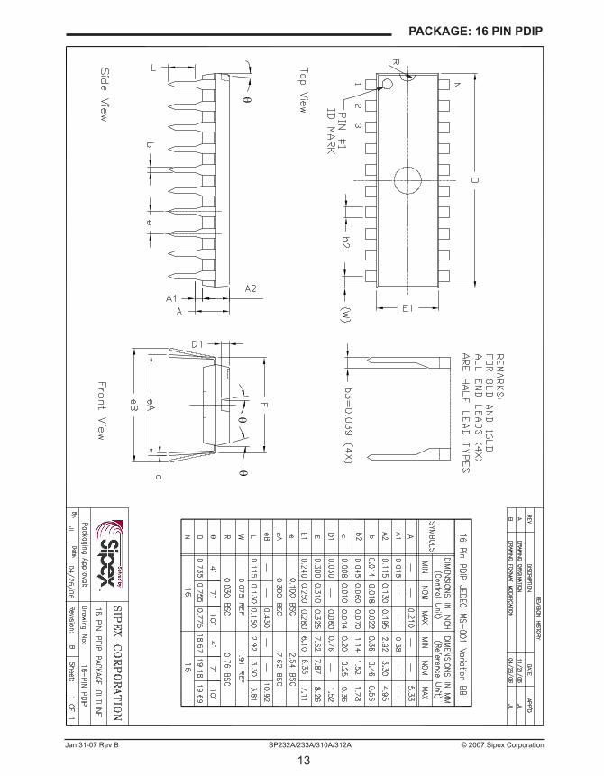
PAckAgE: 16 Pin PDiP

��Jan 3�-07 Rev B SP232A/233A/3�0A/3�2A © 2007 Sipex Corporation
PAckAgE: 18 Pin PDiP
��Jan 3�-07 Rev B SP232A/233A/3�0A/3�2A © 2007 Sipex Corporation
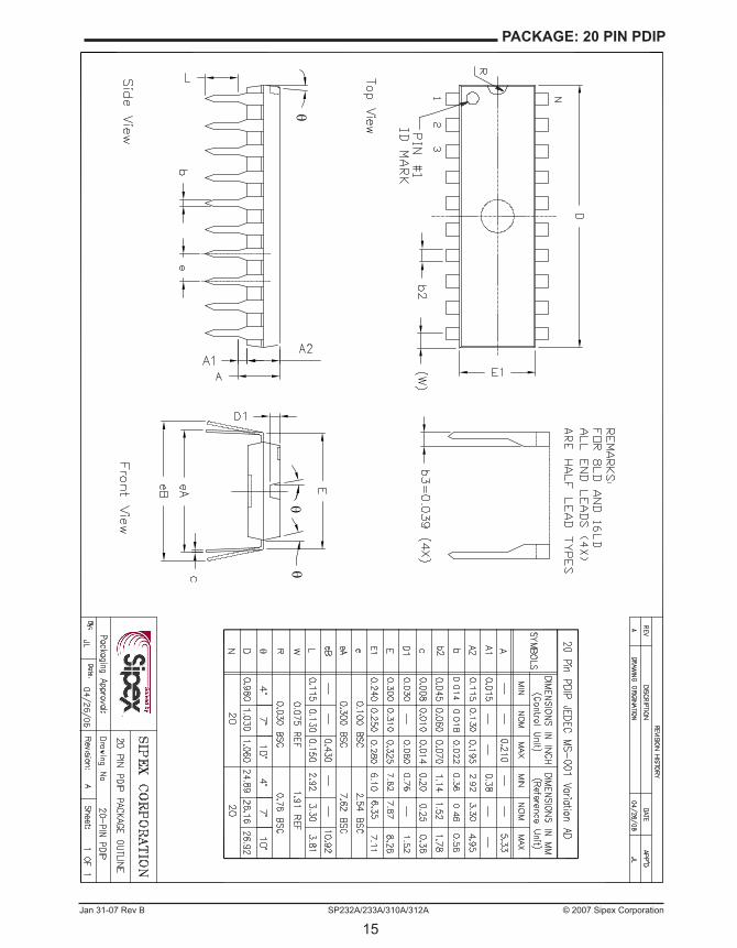
PAckAgE: 20 Pin PDiP
��Jan 3�-07 Rev B SP232A/233A/3�0A/3�2A © 2007 Sipex Corporation PACKAGE: 16 PIN NSOICSolved by Sipextm
Sipex corporation
Headquarters andSales Office233 South Hillview DriveMilpitas, CA ��03�TEL: (�0�) �3�-7�00FAX: (�0�) �3�-7�00
Sipex Corporation reserves the right to make changes to any products described herein. Sipex does not assume any liability arising out of the application or use of any product or circuit described herein; neither does it convey any license under its patent rights nor the rights of others.
Part Number Temperature Range Topmark Package
SP232ACN.............................0°C to +70°C................................SP232ACN..........................................................................16–pin NSOICSP232ACN/TR.......................0°C to +70°C................................SP232ACN..........................................................................16–pin NSOICSP232ACP.............................0°C to +70°C.................................SP232ACP.........................................................................16–pin PDIPSP232ACT.............................0°C to +70°C.................................SP232ACT..........................................................................16–pin WSOICSP232ACT/TR.......................0°C to +70°C.................................SP232ACT..........................................................................16–pin WSOICSP232AEN..........................–40°C to +85°C................................SP232AEN..........................................................................16–pin NSOICSP232AEN/TR....................–40°C to +85°C................................SP232AEN..........................................................................16–pin NSOICSP232AEP..........................–40°C to +85°C................................SP232AEP..........................................................................16–pin PDIPSP232AET..........................–40°C to +85°C................................SP232AET...........................................................................16–pin WSOICSP232AET/TR.....................–40°C to +85°C................................SP232AET...........................................................................16–pin WSOIC
SP233ACP.............................0°C to +70°C.................................SP232ACP.........................................................................20–pin PDIPSP233ACT............................0°C to +70°C.................................SP233ACT...........................................................................20–pin WSOICSP233ACT/TR......................0°C to +70°C.................................SP233ACT...........................................................................20–pin WSOICSP233AEP..........................–40°C to +85°C................................SP232AEP..........................................................................20–pin PDIPSP233AET..........................–40°C to +85°C................................SP233AET...........................................................................20–pin WSOICSP233AET/TR.....................–40°C to +85°C................................SP233AET...........................................................................20–pin WSOIC
SP310ACP............................0°C to +70°C.................................SP310ACP.........................................................................18–pin PDIPSP310ACT............................0°C to +70°C.................................SP310ACT..........................................................................18–pin WSOICSP310ACT/TR......................0°C to +70°C.................................SP310ACT..........................................................................18–pin WSOICSP310AEP..........................–40°C to +85°C................................SP310AEP..........................................................................18–pin PDIPSP310AET..........................–40°C to +85°C................................SP310AET...........................................................................18–pin WSOICSP310AET/TR.....................–40°C to +85°C................................SP310AET...........................................................................18–pin WSOIC
SP312ACP............................0°C to +70°C.................................SP312ACP..........................................................................18–pin PDIPSP312ACT............................0°C to +70°C.................................SP312ACT...........................................................................18–pin WSOICSP312ACT/TR......................0°C to +70°C.................................SP312ACT...........................................................................18–pin WSOICSP312AEP..........................–40°C to +85°C................................SP312AEP...........................................................................18–pin PDIPSP312AET..........................–40°C to +85°C................................SP312AET............................................................................18–pin WSOICSP312AET/TR.....................–40°C to +85°C................................SP312AET............................................................................18–pin WSOIC
Available in lead free packaging. To order add "-L" suffix to part number.Example: SP312AEA/TR = standard; SP312AEA-L/TR = lead free.
/TR = Tape and ReelPack quantity is 1,500 for WSOIC and 2,500 for NSOIC.
ORDERING INFORMATION
Solved by
TM