title final report - esa microelectronics section /...
TRANSCRIPT

Title:Doc. no:Date:
Project
Title
Document number: Author: Date:
Review by: Review date:
Final reportABKREPFNLB2005-03-15
Omnisys Instruments ABGruvgatan 8SE-421 30 Västra FrölundaSweden
Phone+46 (0)31 734 34 00
Fax+46 (0)31 734 34 29
[email protected]://www.omnisys.se
VATSE556454668601
Pages: 57
Advanced Autocorrelator TechnologyESTEC Contract: 11211/94/NL/CN/CCN4
Final report
2005-03-15
ABKREPFNLB
Abstract
This report describes an spectrometer implemented in Multi Chip Module technology, i.e. twonaked ASIC’s mounted on one carrier A matter of fact, two different MCM’s has been developped,one focusing on wide bandwidth, low resolution applications, and one intended for higherresolution applications. The function has been demonstrated in lab tests, as well as by operating afull demonstrator spectrometer in a ground based 110 GHz radiometer.
The specification was 1 GHz bandwidth with 64 and 1024 spectral channels, and with a powerconsumption of less than 1 mW/GHz/channel. The result has been 1.7 GHz bandwidth, 128 and1024 channels resolution, and 0.5 mW/GHz/channel power consumption.
The design, test results as well as application candidates are described in the report.
AE
Stefan Andersson
2005-03-15

Title: Final reportDoc. no: ABKREPFNLBDate: 2005-03-15 Page: i
Table of Contents1. Introduction and Spectrometer Background ............................2
1.1 Overview .............................................................................................. 21.2 Spectrometers..................................................................................... 21.3 Autocorrelation spectrometers examples ........................................ 4
1.3.1 ODIN SPECTROMETER.....................................................................41.3.2 DLR/TELIS SPECTROMETERS.........................................................41.3.3 CURRENT DEMONSTRATOR............................................................51.3.4 Correlator development .......................................................................7
1.4 Project example: STEAM.................................................................... 71.4.1 Summary .............................................................................................71.4.2 Background and scope........................................................................81.4.3 STEAM scientific motivation ................................................................81.4.4 Payload................................................................................................81.4.5 Radiometer concept ............................................................................91.4.6 Radiometer overview...........................................................................9
1.5 Example 2: MAMBO ..........................................................................101.5.1 SCIENTIFIC OBJECTIVES ............................................................... 111.5.2 Radiometer concept .......................................................................... 111.5.3 Specific physical objectives ...............................................................121.5.4 Global objectives ...............................................................................131.5.5 MAMBO Operating Modes Description .............................................13
2 Autocorrelation Spectrometer Background............................152.1 General ACS Architecture................................................................152.2 Correlator Chip Architectures Time and Frequency Multiplexing 16
2.2.1 Hybrid spectrometer signal processing (frequency multiplexed) .......17
2.3 Real and Complex Downconversion...............................................192.4 Quantisation and Power Detection .................................................192.5 Correlator Chip Architectures .........................................................21
3 System Level Optimization.......................................................233.1 High frequency parts ........................................................................243.2 Low frequency parts .........................................................................243.3 Analog to digital quantisation (digitizer) ........................................243.4 Correlator parts .................................................................................243.5 Power and control.............................................................................24
4 Chip Scale Packaging (CSP).....................................................26
Title: Final reportDoc. no: ABKREPFNLBDate: 2005-03-15 Page: ii
Table of Contents4.1 Introduction .......................................................................................264.2 Technology choice............................................................................264.3 Design of Omnisys full custom CSP...............................................264.4 Test set-up .........................................................................................274.5 Test results with CSP........................................................................284.6 Test result comparison.....................................................................294.7 Summary and conclusion ................................................................29
5 Three Level Digitizer..................................................................305.1 Digitizer Design.................................................................................30
5.1.1 Introduction........................................................................................305.1.2 Performance ......................................................................................315.1.3 Technology and Methods...................................................................315.1.4 Functional description........................................................................31
5.2 Digitizer Testing ................................................................................325.2.1 Digitizer Test setup ............................................................................325.2.2 DC characteristics .............................................................................335.2.3 Digital threshold levels.......................................................................335.2.4 Comparator threshold versus reference levels..................................33
6 Correlator chip(s).......................................................................356.1 Correlator Chip Design.....................................................................35
6.1.1 Introduction........................................................................................356.1.2 Technology and methods...................................................................356.1.3 Functional description........................................................................366.1.4 Inputs from quantizer.........................................................................366.1.5 Digital I/O...........................................................................................376.1.6 Power distribution ..............................................................................376.1.7 Correlation .........................................................................................376.1.8 Integration..........................................................................................376.1.9 Prescaler ...........................................................................................386.1.10 Readable integrator ...........................................................................386.1.11 Data readout......................................................................................386.1.12 128 channel implementation..............................................................396.1.13 1024 channel implementation............................................................40
6.2 Correlator Chip Testing ....................................................................416.2.1 Test setup ..........................................................................................416.2.2 Quiescent power consumption ..........................................................416.2.3 Correlator AC power consumption ....................................................42

Title: Final reportDoc. no: ABKREPFNLBDate: 2005-03-15 Page: iii
Table of Contents6.2.4 Maximum correlation data rate ..........................................................426.2.5 Data read-out dynamic power consumption ......................................436.2.6 Results...............................................................................................436.2.7 Conclusions .......................................................................................44
7 Radiation tests ...........................................................................457.1 Device under test ..............................................................................457.2 Test setup ..........................................................................................457.3 Monitored signals .............................................................................467.4 Test procedure ..................................................................................477.5 Results ...............................................................................................47
8. The 6 GHz Spectrometer Demonstrator ..................................488.1 Demonstrator Design .......................................................................488.2 Demonstrator Lab Testing................................................................50
9 Radiometer Test Results...........................................................519.1 Introduction .......................................................................................519.2 Radiometer overview........................................................................519.3 Front-end details ...............................................................................529.4 Back-end and ACS set-up ................................................................539.5 Test results, analyses and discussion............................................54
10 Conclusion and future prospects ............................................57

Title: Final reportDoc. no: ABKREPFNLBDate: 2005-03-15 Page: 1 of 57
57
List of Abbreviations
AOS Acousto Optical Spectrometer
ACS AutoCorrelation Spectrometer
ADC Analogue to Digital Converter
ASIC Application Specific Integrated Circuit
CMOS Complementary Metal Oxide Semiconductor
CCD Charge Coupled Device
CSP Chip Scale Packaging
CTS Chirp Transform Spectrometer
DRC Design Rule Check
DRDP Design Review Data Package
DSP Digital Signal Processing
ERC Electrical Rule Check
LVS Layout Versus Schematic Check
MCM Multi Chip Module
MCM-L MCM based on high density laminated PCB
MPW Multi Project Wafer
PCB Printed Circuit Board
RTL Register Transfer Level
S&H Sample and Hold
SNSB Swedish National Space Board
SSC Swedish Space Corp.
SOW Statement Of Work
TBC To Be Confirmed
TBD To Be Defined
TDM Time Division Multiplexing
VHDL VHSIC Hardware Description Language
VHSIC Very High Speed Integrated Circuit
VLSI Very Large Scale Integration
WP Work Package
WPD Work Package Description

Title: Final reportDoc. no: ABKREPFNLBDate: 2005-03-15 Page: 2 of 57
57
1. Introduction and Spectrometer Background
1.1 OverviewThis report describes an autocorrelation spectrometer implemented in Multi Chip Module technology, Amatter of fact, two different MCM’s has been developed, one focusing on wide bandwidth, low resolutionapplications, and one intended for higher resolution applications. The function has been demonstrated in labtests, as well as by operating a full demonstrator spectrometer in a ground based 110 GHz radiometer.
The integration of quantizer and correlators into a single chip originally foreseen in this activity has provento be unfeasible due to technological constraints, and it has been replaced by a Multi Chip Module (MCM)implementation. It has further been decided to investigate another way of improving the speed/volume ratio,the Chip Scale Packaging (CSP).
The report starts with an introduction to spectrometers and an overview of the ACS technology. This isfollowed by a description of the ASIC designs and test result. Finally, the design, implementation and testresults from a demonstration spectrometer is shown. In addition, results form radiation tests of the chips aredescribed.
The specification was 1 GHz bandwidth with 64 and 1024 spectral channels, and with a power consumptionof less than 1 mW/GHz/channel. The result has been 1.7 GHz bandwidth, 128 and 1024 channels resolution,and 0.5 mW/GHz/channel power consumption.
The design, test results as well as application candidates are described in the report.
1.2 SpectrometersIn many applications when a signal is analysed with high spectral resolution, sometimes in the order of ten tothe power of six or higher, heterodyne receivers are employed. In signal to noise limited applications, such aslimb sounding aeronomy, the system is often divided into a low noise "Front-End" and a spectrometer type"Back-End". Even if the noise level of the spectrometer is uncritical, it must be very efficient, i.e. acommercial swept filter spectral analyser, that process only one "channel" at a time, will not do. The specialenvironment of a satellite will add additional constraining requirements on the design of a "Back-End"spectrometer, such as low power consumption, size and weight. Of course, the quality aspects, such asradiation tolerance, is also of outmost importance.
In its most general form, a spectrometer can be considered to be a device that receives an input signal, whichis variable in time, and estimates its power spectral density. The estimate is given sampled at N equidistantfrequency points, or channels, f0,..., fN-1, separated in frequency by B/(N-1), where B is the bandwidth of thesignal. Critical parameters are the total bandwidth, the transfer function of each channel, H(f), and thestability of the spectrometer. Perhaps most important is that the spectrometer should add as little noise aspossible to the overall system noise budget.
FIGURE 1.1 Submillimetre heterodyne system.
The most widely used spectrometers in aeronomy and radio astronomy are; the Chirp TransformSpectrometer (CTS), the Acousto-Optical Spectrometer (AOS), the Autocorrelation Spectrometer (ACS) andthe Filterbank Spectrometer. Spectrometers based on all types of technology, except the Autocorrelation

Title: Final reportDoc. no: ABKREPFNLBDate: 2005-03-15 Page: 3 of 57
57
type, must be designed with fixed bandwidth and resolution, i.e. they are very inflexible for different kinds ofobservations. The Autocorrelation Spectrometer is in this regard flexible, but has previously suffered from acomparably high power consumption when processing very wide bandwidths. Due to development over thelast 5-7 years, the autocorrelation spectrometer can today, in many cases, beat the alternatives with an orderof magnitude in this respect.
The CTS is based on a chirp filter, that is used for a convolution process to transform the spectra from thetime domain to the frequency domain. The chirp filter sets the bandwidth and resolution limits of a particularspectrometer, and 200 MHz bandwidth has been the upper limit for some time. In addition to the chirp filter,a chirp pulse circuit is needed, as well as a fast and accurate sampling and accumulation function. Access toa chirp filter compliant with the spectrometer requirements is the limiting factor for a CTS.
The AOS is based on a Bragg cell, where the signal to be analysed is feed acousticly in one end of the device.A laser is focused on the cell, and the light is deflected according to the spectral density of the signal. This iscaptured with a CCD. The Bragg cell sets the bandwidth and resolution limits of a particular spectrometer. Inaddition, some optics is needed for handling the light beam processing. From quality aspects, we haveseveral critical parts in an AOS; the laser, the Bragg cell, the CCD and the optics.
In the autocorrelation section the main processing and detection is done in the time domain. This has manyadvantages, one being that the signal can be digitized with very low precision without losing very muchsensitivity, and high speed digital electronics can be used for the processing with all the advantages ofstability and system integration. State of the art autocorrelators use two-bit precision with about 90%efficiency.

Title: Final reportDoc. no: ABKREPFNLBDate: 2005-03-15 Page: 4 of 57
57
1.3 Autocorrelation spectrometers examplesThe autocorrelation spectrometer is one of four types of spectrometers being considered for space based(sub)millimetre heterodyne systems. The advantages of the digital autocorrelation spectrometer compared toChirp Transform, Acousto Optical and Filterbank spectrometers are; stability, compactness, high reliabilityand variability in bandwidth and resolution.
1.3.1 ODIN SPECTROMETERThe ODIN satellite is a joint aeronomy and astronomy mission. The main payload consists of four tunableheterodyne schottky receivers in the frequency range 480-570 GHz and one fixed tuned 119 GHz heterodynesystem. In addition, there is an UV-spectrometer.
There are four back-end spectrometers connected to the five heterodyne systems, two autocorrelationspectrometers, one AOS and one filterbank. The autocorrelation spectrometer and AOS power consumptionare the same, while the size and mass of the AOS is 7 times the correlation spectrometer. The filterbank onlyconsumes 2 W.
The ODIN satellite has been in successful operation for more than 2 years, the design lifetime, and a decisionhas been made to operate for an additional 2 years. The benefits of the variable bandwidth and resolution hasbeen essential.
FIGURE 1.2 The ODIN spectrometer core with 100-800 MHz bandwidth in steps with 0.13-1.1 MHz resolution. Other specifications are: 1 kg, 220x180x30 mm and 18 W power consumption.
1.3.2 DLR/TELIS SPECTROMETERSBased on a chip-set developed during 1998-1999, motivated by MASTER and FIRST, 600 MHz coverageand 256 channels resolution is possible with only two chips, one quantiser and one correlator chip. This canbe used for compact spectrometers as well as more wideband alternatives. Master is an ESA instrument/mission concept for Earth Observation, while FIRST has been renamed Herschel, and is a submillimeterscience mission.

Title: Final reportDoc. no: ABKREPFNLBDate: 2005-03-15 Page: 5 of 57
57
A "standard" spectrometer with 2 x 2 GHz bandwidth, and 2 x 1024 channels has been designed, and two hasbeen ordered for the DLR TELIS project, based on the chip set running at 500 MHz. TELIS is a balloonborne mission with three cryogenic submillimeter receiver front-ends. The spectrometers will be sharedbetween the front-ends, through an IF processor, also designed and delivered by Omnisys.
This is now the standard spectrometer design available from Omnisys, with many possible configurations,and a $100K for a standard (not space level) implementation.
If we compare with available alternatives to achieve 4 GHz total processing bandwidth, we would need 2-4AOS systems, with mass and power consumption in the 10 kg and 50 W class.
FIGURE 1.3 The current generation of spectrometers, with top and bottom views, based on a 256 channel correlator chip and digitizer with 1200 MHz effective sample rate. The box incorporates 2048 channels and configured with 2 x 2
GHz etc.
1.3.3 CURRENT DEMONSTRATORA new chip set has been developed under this contract, with one digitiser and two correlator chips. Thedigitizer has up to 4 GHz bandwidth, and the two correlator chips close to 2 GHz. One of the chips has 128spectral channels, while the other one has 1024.
The number of channels used can be controlled to save power consumption, and the sampling rate can easilybe changed by a factor of 1, 2, 4, 8.
To demonstrate the capabilities, a demonstrator has been designed and tested. The specification for thedemonstrator has followed the Master / Marschal requirements, with 20 W power consumption and 10 kgmass. Master is an ESA instrument/mission concept and Marshal a prototype/demonstrator for this mission.The demonstrator has shown that the performance can be realised with a system of less than 1 kg and lessthan 8 W power consumption. With flight development, the mass could easily be reduced by a factor of two.

Title: Final reportDoc. no: ABKREPFNLBDate: 2005-03-15 Page: 6 of 57
57
FIGURE 1.4 Demonstrator correlator PCB. This PCB incorporates 512 spectrometer channels covering 6 GHz.
One demonstrator has been tested with an 110 GHz ozone radiometer in Bremen, using four correlatormodules, proving the chip sets potential:
• 12 GHz bandwidth (6 GHz implemented in the demonstrator, space available for 12 GHz implementa-tion)
• 1024 channels (512 channels implemented in the demonstrator, space available for 1024 GHz imple-mentation)
• 110x170x30 mm / 800 grams
• 8 Watt
FIGURE 1.5 1024 GHz / 2 GHz Correlator module.
The correlator module is very compact, and can easily be incorporated in many low mass applications.

Title: Final reportDoc. no: ABKREPFNLBDate: 2005-03-15 Page: 7 of 57
57
1.3.4 Correlator developmentIn the table below, examples of the chip development the last decade is shown. Major items of coursebandwidth and system integration level, but for space applications, the power consumption is vital. From thistable, it is clear that the Omnisys chip set.
TABLE 1.1 Correlator chip sets
Now, the chip set is not of interest to the scientist, and not to the system engineer or project manager either, itis the system performance and cost. For this we must look at the specification one step higher, the systemlevel. For the proposal to the HIFI team for Herschel, the Omnisys alternative was 2 kg / 45 W, comparedwith the competitor’s 14 kg / 240 W. (The performance was comparable, and the redundancy cleaner for theOmnisys proposal). As the system difference can not only be explained by the chip power consumptiondifference, this examplifies that focus on system desigh is essential. In addition, the Omnisys proposal wasbased on using packaged correlator chip’s, while the competitor’s was based on complex and large MCM’s.
Now, as a result from the development at Omnisys described in this report, a general conclusion is thatautocorrelation spectrometers are very competitive with other type of spectrometers for space and groundbased (sub)millimeter radiometry. The main advantages are: compact implementations, scalability andversatility in bandwidth and resolution, combined with potentially very high stability.
In terms of size, the correlator is clearly much more compact than either the Chirp or the AOS, an optimisedCTS being 2-3 times the size of a correlator, while an AOS is at least 10 times larger.
In terms of power consumption, the CTS is comparable to the ACS for narrow bandwidth, while the AOSconsumes 2-4 times more than the ACS for wide bandwidth applications. The CTS can not compete for widebandwidth applications, while the AOS is not competitive for high resolution use.
In terms of flexibility in bandwidth and resolution, the CTS and the AOS have very limited capabilities.
The ACS uses no special technologies and components, such as lasers, CCD's, Bragg Cell's or Chirp filters,with concerns regarding availability, radiation tolerance and other quality concerns. The only specialtechnology is the full custom design of the chip set, while a $1000 Billion industry helping in the productionline set-up. The NRE for the ASIC's are about $100-150 K. To this, qualification cost must be added, but incomparison with the ACS and AOS, no comparable qualification methods exists for Chirp filters, CCD’s,Lasers or Brag cells.
1.4 Project example: STEAM
1.4.1 SummaryThe Stratosphere-Troposphere Exchange And climate Monitor (STEAM) project is technically feasible. Theproject addresses important goals for atmospheric scientists regarding climate research and the instrumenttechnology needed is at hand, mainly through the previous Odin project. The project has the explicit supportof research groups in at least three countries, and potentially in several other countries and in ESA. SinceSTEAM can build on methods and technology already developed for Odin, SMART-1 and other projects, thecost and risks should be lower than for Odin. Also, STEAM is in several ways a simpler system than Odin.The concept assumes daily operations to be conducted from SSC Esrange, near Kiruna.
mW # GHz mW/#/GHzBos 1000 16 0.02 3125.00 1992 state of the artOmnisys-ODIN 400 96 0.1 41.67 2 chips, works in space, 1996Omnisys&ESA 1100 256 0.6 7.16 2 chip, 1999French HIFI 500 128 0.2 19.53 3 chip, 2001??Omnisys&ESA: S 230 128 2 0.90 2 chip, 2002Omnisys&ESA: L 1750 1024 2 0.85 2 chip, 2002Spaceborne 5500 128 2 21.48 1 chip, 2003Omnisys SCS 1200 1024 4 0.29 1 chip, planned

Title: Final reportDoc. no: ABKREPFNLBDate: 2005-03-15 Page: 8 of 57
57
1.4.2 Background and scopeIn 1998 European scientists proposed to the ESA Explorer program a follow on mission to Odin namedSCOPE (Stratospheric Chemistry Opportunity Explorer) similar to STEAM but without holographiccapability. It was recommended by the evaluation committee but not selected. An advanced, imaging versionof this instrument was proposed to CNES (MOST — Microwave Observations of Stratosphere andTroposphere) in 2001. The study demonstrated that the UT/LS part of the payload could fly as amicrosatellite payload. STEAM was proposed in response to the SNSB call for ideas in 2002 and in thesummer SSC was awarded a contract for a technical feasibility study of the Stratosphere- TroposphereExchange And climate Monitor (STEAM) project. The study is aimed at defining at least one possiblesystem configuration that would fulfil the scientific objectives of the project and estimating its cost andschedule. Included in the study was a smaller part aiming at identifying possible Swedish contributions to aFrench instrument for sounding the Mars atmosphere, MAMBO. The MAMBO part should addressdevelopment status, synergy with the STEAM radiometer development and cost of the contributed hardware.Since the French Mars-probe Premier project was discontinued, less effort was spent in the study on thepossible synergy between the two radiometers.
An important part of the study was directed to Omnisys Instruments, as subcontractor to SSC, for studyingkey parts of the radiometer equipment. The results of the study are summarised in the following.
1.4.3 STEAM scientific motivation In summary, STEAM is dedicated to the investigation of chemical, dynamical, and radiative processes in theupper troposphere and lower stratosphere (UT/LS) altitude range and their links with the Earth climate andstratosphere evolution. The main objective is to provide vertically and horizontally resolved information onthe global distributions of UT/LS key species such as water vapour (H2O), ozone (O3), and carbonmonoxide (CO), and global fields of O3, H2O and halogen compounds responsible for the O3destructionlike chlorine monoxide (ClO) in the stratosphere. The UT/LS region plays an important role in the Earth’sclimate system. Despite its importance there is still a lack of accurate, heightresolved data in the UT/LS.Confronting 3-D climate and chemical-transport models with STEAM observations will improve ourknowledge on this critical atmospheric region.
Furthermore it is of vital importance to monitor on a global scale the evolution of the stratosphere beyond2007 in order to quantify the expected decline of halogen compounds and check whether the ozone layer isstarting to recover.
Radiative aspects will in particular be addressed by the measurements of H2O, O3, and N2O. Well resolvedSTEAM data of H2O, O3, CO, N2O, and CH3Cl in the UT/LS will allow studying dynamical processes suchas stratosphere-troposphere exchange or transport between high-, middle and low-latitudes. Chemicalaspects cover both the upper troposphere (O3budget, biomass burning, aircraft impact) and the lowerstratosphere (ozone evolution) and will be investigated using the global dataset of H2O, O3, CO, N2O,HNO3, HCN, and CH3CN.
Thus, the three main research areas are climate evolution, stratosphere-troposphere exchange, and ozone inthe troposphere and stratosphere. STEAM is supported by French, Swedish and Canadian laboratories,gathering the tropospheric and stratospheric science communities in these countries. It should also be notedthat the scientific objectives cover at large part of the objectives of the ACECHEM project, proposed toESA. ACECHEM was proposed by aeronomers of 13 institutes in 7 countries. It was highly rated forscientific merit but was not chosen for further studies within the ESA framework due to an estimatedexcessive cost. Thus, several other countries and ESA can be considered potential partners in the STEAMproject, at least from a scientific-interest point of view, yet we have to reduce cost.
1.4.4 PayloadThe main instrument on STEAM shall be a radiometer for mm and submm wavelengths, complemented byan optical instrument, partly similar to OSIRIS on Odin. The radiometer shall operate in the 320-360 GHzrange to sound the UT/LS and in the 485-505 GHz range to sound the stratosphere. Using a unique techniquefor sounding the Earth atmosphere’s limb from 5 to 28 km by employing 8 simultaneous measurements,

Title: Final reportDoc. no: ABKREPFNLBDate: 2005-03-15 Page: 9 of 57
57
STEAM shall produce a global data set of UT/LS key species with both a good vertical (1.5-2.5 km) and agood horizontal resolution (30-50 km). The mm band shall have the same line-of-sight as the opticalinstrument, which shall measure aerosols and clouds. The submm band shall cover 15 to 40 km in altitude,also with 8 simultaneous measurements. For the mm band the spectrometers shall have a maximuminstantaneous bandwidth of 8 GHz at a resolution of 10-20 MHz. For the submm band the bandwidth shall be4 GHz (2 GHz processed) and the resolution 2 MHz.
1.4.5 Radiometer conceptThe telescope views thermal emission from the atmospheric limb imaged by a small linear array ofheterodyne receivers in the instrument platform. The incoming radiation is down converted and amplified inthe receivers. Spectrometers measure the spectral power density across each band, and digitised outputs aresent via the data interface to the spacecraft system to be eventually made available for ground processing.
The radiometer design is basically a simplified Odin design. Compared to Odin we do not foresee a need forpower demanding active cooling, frequency tuning, single sideband operation and fundamentally pumpedmixers. This makes it possible to build a simplified system with mixers directly fed by the telescope andpumped via wave-guides. It is then possible to build a multi-beam system and use novel tomographicmethods to overcome one major limitation of the current limb scanning technique — the poor horizontalresolution. The telescope surface accuracy can be relaxed by a factor of 2 compared to Odin.
The telescope would be built and tested using the now proven Odin methods and would be an off axisGregorian design with an elliptical (1 m × 0.5 m) main reflector constructed of carbon fibre composite(CFRP) for thermal stability. Its support structure could be built in the shape of a CFRP box that also housesthe optics, calibration sources, LO units with phase lock electronics and the mixer assemblies.
There will be optics to provide means for calibration and for switching towards cold space. In this modifiedOdin scheme the receiver signals are separated by means of a polarising grid, creating two sets of 4 beams.Further separation is achieved by imaging the focal plane onto the set of mixer horns. All eight receivers thusreceive the signal from different parts of the limb simultaneously. A mesh filter can be included to suppresshigher harmonics of the sub-harmonically pumped Shottky mixers. HEMT based low-noise amplifiersmounted next to the mixers will provide the first amplification. With InP-Gunn oscillators there is sufficientpower for one LO to pump four mixers. The units would be phase locked, using almost the identical designto Odin’s. They would drive either a Varactor or the Gunn voltage to correct for the error signal determinedby comparing the harmonic from the 86 GHz range to an internal reference source locked to a stable lowfrequency clock source. LO chain designs based on multipliers and power amplifiers is also an alternative,and this is under development at Omnisys and will be demonstrated during Q1 of 2004. The backends arerequired to select and process the frequency regions surrounding the molecular lines of interest, synchronisedto instrument pointing and reference switching. Autocorrelator spectrometers will be used as backends. Theautocorrelator, being a digital processor, is well adapted to space use and is inherently stable. ESA has withinthe technology research program developed, for future limb scanning missions, a more modern and in manyways improved correlator chip compared to the Odin design. In the case of a limited power budget, one coulduse a reduced number of autocorrelators for the bands, where the mixer outputs are time-multiplexed to thebackends. However, this would compromise sensitivity and/or spatial resolution. These tradeoffs requirefurther investigation.
1.4.6 Radiometer overviewThe baseline system design for STEAM is to cover several atmospheric lines of interest, split on two mainfrequency bands, 320-360 GHz and 495-503 GHz. This requires two sets of front end receivers, and that the320-360 GHz is tuneable.
The baseline is also to utilise linear arrays of receivers to cover different altitudes in parallel, simplifyingmechanics as well as increasing the efficiency. This is planned to be implemented with two sets of fourreceivers for each band, the two arrays working with different polarisation, for minimum sampling distance.

Title: Final reportDoc. no: ABKREPFNLBDate: 2005-03-15 Page: 10 of 57
57
FIGURE 1.6 Steam radiometer system overview.
These four arrays of four receivers need access to the sky with four horns, the IF outputs of 4 times 8 GHz(6-14 GHz TBD), as well as LO to all receivers.
The output from the IF amplifiers are then feed to an IF system, followed by spectrometers. The LO (andbiasing) will be provided as by a Front-end Control system.
Main characteristics• Multibeam (simplified optics) and developed as an integrated instrument• 8 front-ends at 320-360 GHz, DSB (simplified optics)• 8 front-ends at 490-505 GHz, DSB (simplified optics)• 8x8 GHz + 8x4 GHz = 96 GHz of spectrometers• operation in ambient temperature (simplified system) with 2000 K Tsys (prel)• a few kgs, 60-70 W total payload power consumption.• on-board, near real-time signal processing (Linux)
1.5 Example 2: MAMBOThe MAMBO (Mars Atmosphere Microwave Brightness Observer) instrument was intended for the French-led mission to Mars, PREMIER, later cancelled due to financial problems. This would have been the firsttime the atmosphere on another planet had been investigated in detail. There was both scientific, dataprocessing and technical overlap between STEAM and MAMBO. The MAMBO receiver is basically asingle channel STEAM receiver but requires higher spectral resolution due to the low pressure on Mars.Both have the same requirements for high bandwidth to covering the somewhat widely spaced spectral lines.There were substantial synergy effects between the instruments. For instance, it would be possible to use aSTEAM mixer block with its local oscillator and phase lock system unchanged for MAMBO.
Compared to the old MAMBO design, partly based on traditional hardware from space industry and fromJPL, both size, mass and power can be substantially reduced. Based on the investigations made so far, it isproposed to carry out a feasibility study (“Phase 0”) regarding the possibility to build a Swedish low-cost,low-weight alternative to the MAMBO instrument. This instrument could be accommodated on a Marsmicro probe, proposed within another study for SNSB (Swedish National Space Board) as one of the
CNTFE cntIF sys
PayloadcontrollerPayloadcontroller
BackEnd
PWR
CNTFE cntIF sys
BackEnd
PWR
CNTFE cntIF sys
BackEnd
PWR
CNTFE cntIF sys
BackEnd
PWR
495A
495B
340A
340B
PayloadPower
DistributionUnit
28 VSystem bus
Systemcnt/data
busCnt/data
developmentbus

Title: Final reportDoc. no: ABKREPFNLBDate: 2005-03-15 Page: 11 of 57
57
alternatives for a technology research satellite (“Tsat-Mars”).
FIGURE 1.7 Simulation of a limb spectrum (tangent altitude: 10km) around 320-350 GHz in typical Martian conditions for a MAMBO-like instrument.
1.5.1 SCIENTIFIC OBJECTIVESThe microwave sounder MAMBO aims to characterize the dynamics and the composition of the Martianatmosphere, with an unprecedented sensitivity. For this purpose, MAMBO will analyse the thermal emissionof the atmosphere at microwave frequencies using heterodyne spectroscopy, for the first time from orbitaround another planet.
In practice, MAMBO will perform measurements at the atmospheric limb and at nadir using a receiverdedicated to the monitoring of selected lines of key molecules in the range 320-350 GHz:
• CO at 345.796 GHz • 13CO at 330.588 GHz• H2O at 325.153 GHz• HDO at 335.395 GHz• O3 at 326.901 GHz• H2O2 at 326.981 GHz
1.5.2 Radiometer conceptThe radiometer concept is based on two identical subsystems, both covering the frequency band of interest,as shown below.

Title: Final reportDoc. no: ABKREPFNLBDate: 2005-03-15 Page: 12 of 57
57
FIGURE 1.8 Mambo radiometer block diagram.
The basic idea is to have redundancy, and with both systems operating, we have an improved systemperformance by an effective reduced system noise temperature with a square root of two.
There are several advantages of using an ACS compared with CTS, that also has been considered. The mainaspect is the flexibility in bandwidth and resolution, but also the wide bandwidth possibilities of a modernACS. From system level perspective, this reduce the mass and power consumption with at least a factor offour.
1.5.3 Specific physical objectivesThe instrument performances will allow the 3D mapping, with an excellent spatial cover, of the followingphysical items:
Wind:
The MAMBO high spatial resolution allows to make use of the line profiles and their Doppler shift. Limbviewing allows a direct measurement of the winds on Mars from orbit. Both 13CO and CO will be used tomonitor the atmosphere from 20 km to 130 km, with a vertical resolution better than 10 km and an 10 m.s-1-accuracy.
Temperature:
From the planet surface up to 120 km. The temperature profile will be retrieved from CO and 13CO lines.This will allow an unprecedented accuracy, especially during periods when the atmosphere is dust laden.
Water Vapour:
Using the H2O and HDO lines will allow measuring water vapour profiles from near the surface up to 60km, with an accuracy and a sensitivity much better than previous experiments.
D/H Ratio:
This isotopic ratio will be obtained by simultaneous spectroscopy of H2O and HDO. Monitoring D/H ratio isa key investigation to understand the evolution of water on Mars.
Ozone:
Ozone profile will be measured accurately up to 70 km, simultaneously with water vapour. This will allow us
x2
YIG
Activex4
subharm onicm ixer
M ixer b iasLNA biasx 2 b ias
Phasenoise+ Freq re fFreq. cn t
m onito ringtuning
LN A3-14 G HzH
V
x2
170G Hz/3 m W
10.5 G Hz
x2
YIG
Activex4
M ixer b iasLNA b iasx 2 b ias
Phasenoise+ Freq refFreq. cnt
m onito ringtuning
x2
IF-system andspectrom eters
3-14 G Hz
PW RC NT
CPU
PW RCNT
28 V
TM /TC
TM /TC
28 V
CPU
IF-system andspectrom eters
42 GH z

Title: Final reportDoc. no: ABKREPFNLBDate: 2005-03-15 Page: 13 of 57
57
to better understand the relationship between the two species. Ozone and Water vapour are supposed to anti-correlated.
Hydrogen Peroxyde (H202):
This species has never been observed on Mars, yet. Several models have shown its key importance for thephoto-chemistry of the Martian atmosphere (control of H2, O2 and CO) and for its role in oxydizing theMartian soil, a key issue for exobiology.
Carbon Monoxyde:
The observation of the strong 12CO line simultaneously with the weaker 13CO line will allow to estimateCO vertical profile with an accuracy of 10-15% up to 90 km in limb viewing.
Surface Science:
Careful analysis of the brightness temperature will thus allow the mapping of the variations of surfaceemissivity e and possibly the thermal inertia of the subsurface.
1.5.4 Global objectivesAtmospheric dynamics and comparative meteorology:
The simultaneous knowledge of the zonal wind and of the thermal structure of the atmosphere combinedwith state-of-the-art techniques of data assimilation in General Circulation Models will allow us to determinethe 3D atmospheric circulation day after day.
Water cycle:
In combination with the observation of the General Circulation, the 3D mapping of water vapour shouldallow us to characterize water vapour transport by the atmosphere and locate its sources and sinks.
A global view of Martian atmosphere photo-chemistry
H2O, O3, H2O2 and CO are key species for the photochemical equilibrium of the Martian atmosphere andits interaction with the surface. The observations of the temporal and spatial variations of these species willbe interpreted in light of a 3D photochemical model, allowing a true understanding of the processes involvedand their coupling.
FIGURE 1.9 Scanning.
1.5.5 MAMBO Operating Modes DescriptionWhen MAMBO is fully operating (beside OFF, stand-by, TM/TC modes), MAMBO will combine severalmodes of observation in which be operated in four main modes. MAMBO antenna will alternately look at:
1. One or several points between Nadir and Nadir±70° (integration time per point: 1 - 5 s)
2. The limb on one side (see details below)
3. The cold calibration target (cold sky above the limb)
4. The internal calibration hot load

Title: Final reportDoc. no: ABKREPFNLBDate: 2005-03-15 Page: 14 of 57
57
MAMBO will repeat the same operations on the other side (modes baseline) or on the same side (in somespecific operating modes).
The observing strategy at the limb is a key issue. A few inputs regarding the limb strategy are:
MAMBO antenna will rotate preferentially step by step. A constant angular rate would be considered if it isshown to strongly simplify design considerations.
MAMBO will acquire one spectrum every 5 km (limb vertical projection).
The angular rate of the antenna will be suited to a limb scanning velocity of 3 ± 2 km/s. The correspondingangular rotation rates is given in the table below.
Limb scanning shall be performed in the range 0 km to 120±10 km. Margins are required on both sides ofthis scale depending on the strategy fostered to identify the limb / surface border on the basis of theinformation provided by the orbiter main CPU and/or from the detection of the limb by the instrument itself.
FIGURE 1.10 Limb scanning.

Title: Final reportDoc. no: ABKREPFNLBDate: 2005-03-15 Page: 15 of 57
57
2 Autocorrelation Spectrometer Background
2.1 General ACS ArchitectureIn a digital autocorrelation spectrometer core, the signal is first translated and conditioned in a few analogprocessing steps before the digitizing and correlation.
FIGURE 2.1 Autocorrelation spectrometer.
The digitized signal is delayed in a number of discrete steps, and the delayed samples are multiplied with anundelayed version of the same signal. The products from the multiplications are then integrated andaccumulated separately for each of the delay stages. After a specified integration period, usually of the orderof seconds, the autocorrelation function is transformed to the frequency domain to form the power spectrum.The autocorrelation spectrometer is based on Wiener-Khintchines theorem;
where
S(w) =power spectrum
R(t) =autocorrelation function
This is the theoretical foundation of the autocorrelation spectrometer, but the digital implementation differsin a number of points from the equations outlined above. The main differences are
• (i)the data is discrete in time
• (ii)the data is discrete in amplitude and very coarse
• (iii)the data set is finite
• (iv)reduced total power dynamic range
Point (i) is taken care of by the Nyquist criteria, i.e., as long as we sample with a rate twice the inputbandwidth or higher, the sampled values contains all the spectral information. In reality, the signal is sampledat a slightly higher rate to accommodate the finite slope of the filter preceding the digitizer.
That the data is sampled with very coarse accuracy, usually with one or two bit precision, has twoimplications. The major is that the signal to noise ratio is degraded, but for a 1.5-bit autocorrelator, thedegraded efficiency is still better than 90%, and can be compensated by using a slightly longer integrationtime. While the theoritical degradation is listed in Table 2.1., as a function of number of bits used, the actualdegradation depends also other factors, such as the statistics of the input signal. The other implication is thatthe correlation estimate is biased, but this is easily taken care of in the processing steps preceding theFourier-transform.
The coarse quantization reduces the sensitivity but it also creates new spectral components [VanVleck&Middleton 1966]. These effects are actually one and the same: the spectral power "leaks" from theoriginal band and creates the new features. The well known effect that sampling at a frequency higher thanthe one specified by the Nyquist criteria increases the sensitivity results from the fact that some part of theleaked power is also covered in the processed band.
The reduced dynamic range only applies to the total power variations, not the peak power in one channel andis usually not a problem. The practical total power dynamic range is 2-3 dB for a fixed system for a reducedsensitivity of less than 2%, however, various gain adjustment features are commonly used providing 10-20

Title: Final reportDoc. no: ABKREPFNLBDate: 2005-03-15 Page: 16 of 57
57
dB total power dynamic range or more. Both attenuators and variable gain amplifiers as well as adjustableADC reference levels can be used.
2.2 Correlator Chip Architectures Time and Frequency MultiplexingFor the overall architecture, we have various design choices to achieve wide bandwidth. In Figure 2.2, astraightforward autocorrelation spectrometer is shown. It consists of a filter with 1.2 GHz bandwidth, anADC operating at 2.6 GHz and a 32 channel autocorrelation block, also operating at 2.6 GHz. The resultingspectrum would consist of 1.2 GHz wide band divided into 32 spectral channels.
FIGURE 2.2 A straightforward autocorrelation spectrometer. The 2.6 GHz sampling rate is chosen to be twice the input bandwidth plus a small oversampling factor to accommodate the finite slope of the filter.
In Figure 2.3, a frequency multiplexed (or sometimes referred to as hybrid) autocorrelation spectrometer isshown. It consist of two 600 MHz wide filters, two ADC´s working at 1.3 GHz clockrate, each attached to a16 channel autocorrelation block, also operating at 1.3 GHz. The resulting spectrum would consist of 1.2GHz wide band divided into 32 spectral channels.
FIGURE 2.3 A frequency multiplexed autocorrelation spectrometer. The 2.6 GHz sampling rate is chosen to be twice the input bandwidth plus a small oversampling factor to accommodate the finite slope of the filter.
In Figure 2.4, a time multiplexed autocorrelation spectrometer is shown.
FIGURE 2.4 A time multiplexed autocorrelation spectrometer. The 2.6 GHz sampling rate is chosen to be twice the input bandwidth plus a small oversampling factor to accommodate the finite slope of the filter.
It consist of filter with 1.2 GHz bandwidth, an ADC operating at 2.6 GHz, a serial to parallel converter withtwo output data streams at 1.3 GHz clockrate. These two data stream feed two 16 channel autocorrelationblock, also operating at 1.3 GHz. The resulting spectrum would consist of 1.2 GHz wide band divided into32 spectral channels. The overhead to accommodate time multiplexing is small if the number of channels ineach bank is kept sufficiently high, i.e. 16-32 or higher.
The frequency and time multiplexing approaches can be combined, and a design choice depends on availabletechnologies, size and power constraints as well as functional specification. The major trade-off between

Title: Final reportDoc. no: ABKREPFNLBDate: 2005-03-15 Page: 17 of 57
57
time multiplexed and frequency multiplexed designs can be for power consumption. The frequencymultiplexed design can help to reduce the power consumption for wide bandwidths.
There are four alternative architectures if we include the combination of a time multiplexed and frequencymultiplexed design. We can summarize the major the advantages/disadvantages as:
• Straightforward: best choice if the bandwidth and power consumption can be accommodated with both the ADC and the correlator section clocked at a frequency of twice the processed bandwidth.
• Frequency multiplexed: best choice if neither the ADC nor the correlator can be implemented with the specified bandwidth, or if the power consumption is too high. It is not as amplitude stable as the other two methods.
• Time multiplexed: best choice if the ADC but not the correlator can be efficiently implemented with a clock rate of twice the input bandwidth
2.2.1 Hybrid spectrometer signal processing (frequency multiplexed)The different processing steps in an autocorrelation based hybrid spectrometer are described below, startingwith the hardware section, i.e. filtering, mixing, digitising and correlation. This is then followed by thesoftware section where the data is corrected for the digitizer effects, Fourier transformed and, if a hybridapproach is used, the subspectra are joined to form a continuous spectrum.
Let us denote the spectrum of the input signal s by
Sin (ω),
where S is an ergodic signal with slightly filtered white noise characteristics. After the analogue processing,i.e., filtering, mixing and gain adjustment, we get
where the signal is split up in M frequency subbands, Sm(ω), by the filter functions Fm(ω). M equals unity ifa none hybrid approach is used. Each signal is then quantized and multiplied by a delayed version of itself toform an autocorrelation estimate. As the autocorrelation function is defined in the time domain, thefollowing two stages are treated in that domain, where the analogue and digitized representation of Sm(ω) aredenoted sm(t) and zm(nT), respectively.
FIGURE 2.5 Hardware based processing in a hybrid spectrometer.
The digitization process consists of two parts: sampling of the signal at discrete time intervals, t=nT, andquantization of the amplitude. The quantization function q(x) for a 2-bit correlator is described in Figure 2.2.
After the digitization, we have the autocorrelation estimate r(kT) formed by the function
where kT is the delay. N is usually a very large number and the number of delay lags range from a few to a
1 1S S F S S F S S Fin m in m M in M( ) ( ) ( ), ( ) ( ) ( ), ...., ( ) ( ) ( )ω ω ω ω ω ω ω ω ω= = =
r kTN
z nT z nT kTm mn
N
m( ) ( ) ( )=−
+=
−
∑11 0
1

Title: Final reportDoc. no: ABKREPFNLBDate: 2005-03-15 Page: 18 of 57
57
few thousand.
FIGURE 2.6 Software based processing in the hybrid spectrometer.
In the hybrid spectrometer, the software plays as important a role as the hardware. The data is accumulated inthe time domain as autocorrelation functions and the data must be transformed to the frequency domain.Known instrumental effects should also be removed. However, all processing steps could be performedeither on-board or at a later stage on ground.
The readout autocorrelation estimate stored in the lag registers has systematic, but known errors, and can notbe used directly. The first stage of the software processing is to translate the quantized autocorrelationfunction, rm(kT), into a normalized analogue one with as little bias as possible. The operator, Q, which isderived in [Emrich 1992], takes care of this process. The corrected autocorrelation function is
The quantization correction can not be expressed in a simple equation. The correction is dependent on thethreshold and shown above, the function is plotted for two different values. The correction is specific for thistype of correlator and is dependent on the relative threshold level v0/σ (relative compared to the input rmsvoltage). Because the quantization correction is not a simple equation, it is normally implemented with apolynomial fit. As the quantisation correction is performed on ground, a high order polynomial can be used,however, for more compact code in an embedded system, the correction could be divided into 2-3 regionswith 5-7 order polynomials used for each region.
This is followed by a Fourier transform and scaling with total power information derived from the zero lag orfrom a separate total power detector (see [Emrich 1992])
where pm is the total power estimate of each subspectrum and ωi indicates that the spectrum is sampled indiscrete channels. The number of spectral channels is often chosen to equal the number of delay lags, butboth fewer (smoothing) and more (interpolating) can be used. The autocorrelation function is both real andeven, and the Fourier transformed spectrum is also real and even. Even if an FFT is sometimes used for thetransform, the number of spectral channels will equal the number of autocorrelation channels. Depending ontransform used, the input data must be manipulated to fulfil the even and real criteria, i.e. mirroring the dataaround zero to create the even data set for a cosine transform.
The continuous spectrum is obtained for hybrid spectrometers by joining or linking the subspectra. Thepossible implementations of the linking operator are discussed in [Emrich 1992]. A straightforwardimplementation is to sort the spectral "channels" by frequency and not use the "channels" where thesubbands overlap.
We have now derived an unbiased estimate of the combined power spectrum at the filter outputs. To gofurther and remove the effects of filter and amplifier responses a differential measurement is used, i.e.,
where S*(ω) denotes the power spectrum with a "perfect" filter response and FM(ω) describes the combinedfilter effect of all components in the system preceding the digitizers. S*off(ω) denotes a power spectrumestimated in the same way as S*on(ω), but with the antenna pointing towards a clear sky instead of at the
′ =r kT Q r kTm m( ) ( )
′ = ′S p r kTm i m m( ) F ( ) ,ω
SS S
SS F S F
S Fon off
off
on M off M
off M′ ′ ≈ ′ − ′
′≈
−( )( ) ( )
( )* ( ) ( ) * ( ) (
* ( ) ( )ω
ω ωω
ω ω ω ωω ω
)

Title: Final reportDoc. no: ABKREPFNLBDate: 2005-03-15 Page: 19 of 57
57
source of interest. If FM(ω) is constant with time and signal power is about the same between the on and offspectra, the filter response effects will be removed. Variations on the differential method can be used forother calibration procedures, such as hot/cold load methods, the concept is the same; measure the frequencyresponse over the band and apply it to the uncalibrated spectrum. The differential measurement process alsocancel to the first order the spectral distortions in the receiver front-end.
2.3 Real and Complex DownconversionIn the traditional autocorrelator design, the frequency band to observe is downconverter to baseband beforeanalog to digital conversion. The translation can be implemented with either a chain of filters and mixers, orusing a standard single sideband filter solution, as used for the ODIN spectrometer. The benefits of the SSBmethod is a reduction size as well as power consumption, but also some added flexibility, but the sidebandrejection may be limited to some 25-27dB.
The subcircuits limiting this rejection is mainly the wideband phaseshifters needed, as shown in figure 2.7,but there exist alternatives. One of these is to perform a complex correlation instead, with the sidebandseparation in the post processing stage. Apart from removing circuitry, and the associated errors, thisfacilitates additional post processing clean-up, by measuring phase and amplitude mismatches.
FIGURE 2.7 Real time and complex sampling implementations.
In summary, the benefits of the complex sampling:
• The complex sampler does not require high quality single-sideband filtering (the matched 45 degree phase delays and summation block in Figure 2.12) of the analog input signal. This can significantly reduce the design effort when building a spectrometer.
• The complex sampling frequency is half the sampling frequency used by a real quantizer. The effective sampling frequency will remain the same, since twice as much data is produced per sample.
The complex sampling method has been chosen for the spectrometer chip set in this project.
2.4 Quantisation and Power DetectionThe analog to digital converter should quantize the signal into a number of states, sample the signal in thetime domain and encode the states into digital word. The order of these three stages may vary as well as theencoding scheme. As an example, the quantizer mapping function for a 1.5 bit and 2-bit correlator is shownin Figure 2.8.
delayphase90°
45°phasedelay
-45°phasedelay
quantizer
Real
correlator
Real
filterLP
LO(band lower end frequency)
IF
Sample clock2200MHz
delayphase90°
filterLP
filterLP
quantizer
Complex
correlator
Complex
LO(band center frequency)
IF
Sample clock1100MHz
I
Q

Title: Final reportDoc. no: ABKREPFNLBDate: 2005-03-15 Page: 20 of 57
57
FIGURE 2.8 The quantization function q(x) for two bit converters to the left and for 1.5-bit converters to the right.
The ADC can be operated with a normalized signal level compared with the reference levels or used with avarying signal level. With an un-normalized signal, the zero-lag from the autocorrelation function can beused as a total power estimate. For a normalized operation, a separate total power detection scheme isneeded.
The normalization can be implemented in two ways; adjusting the gain of the input signal, or adjusting thereference levels of the ADC. The latter has the advantage that non-symmetric errors could be compensatedfor, such as an offset in one comparator.
For wide bandwidth systems with a critical ADC specification, the use of a separate total power detectorcombined with an ADC output monitor relax the ADC specification in areas such as DC-drift and symmetry.
The total power detector could be based on an ordinary temperature compensated diode detector system,while the ADC monitor consist of counters, each monitoring the number of samples in each output state.This information would then be processed and used to adjust the ADC reference levels through a digital toanalog converter (DAC). The adjustment can be made in real-time or as a part of a calibration procedure.
One of the main issues in the design of digital correlators is the quantization method chosen. If the signal isconsidered to consist of filtered white noise, a very coarse quantization give very little efficiencydegradation.
The common model to calculate the degradation in efficiency, i.e. the derived noise floor after a fixedintegration time compared to an ideal detector, is based on pure white noise with a time sample to timesample correlation of zero. The math involves a lot of work, but fortunately, this work has been done for us.From [Emrich 1992], [Cooper 1969] and [Hagan&Farley 1973], we can summarise a number of quantizationmethods and their efficiency factors, as shown in Table 2.1.
TABLE 2.1 Correlator quantization
The efficiency factor can further be increased with oversampling the signal, i.e. increasing the correlation

Title: Final reportDoc. no: ABKREPFNLBDate: 2005-03-15 Page: 21 of 57
57
factor. Most gain is achieved for coarse quantization, and in the table, the popular reduced multiplicationscheme 2x2 bit is shown with an oversampling factor of two. The efficiency was increased from 0.88 to 0.93.It should be noted that these calculation are based on the simplification that the channel to channelcorrelation is zero, which actually gives low estimates for the real efficiency. For 1x1 bit correlators, theefficiency can be better than 0.7.
For 1.5-bit, Omnisys has measured between 85-93% efficiency, on the HIFI demonstrator Complexcorrelator design.
2.5 Correlator Chip Architectures A correlator chip architecture can be made with a simple architecture. Two data streams should be multipliedwith each other, one undelayed version of the signal and one that is delayed in a number of stages. The resultshould be accumulated for each delay stage.
The delay circuit could be implemented in two ways, a straightforward way with one delayed and oneundelayed datapath in parallel, or with an xy-architecture. In the xy-architecture the data goes in twodirections. For an autocorrelator, the data output from the end of the x-delay chain is fed to the y-input.
FIGURE 2.9 Two different data flow architectures, the straightforward approach to the left and the xy-type to the right.
In the straightforward implementation, the lag closest to the inputs is the zero-lag. This makes it simple touse variable length autocorrelation estimates (to save power) by shutting down the higher lags when not inuse. The cascading of chips is also easier for the straightforward architecture. For the chips in this report, themajor implication is that with the straightforward implementation, the design can be made asynchronous,with reduced power consumption and/or higher clock speed.
A very useful option is to incorporate a quantizer monitor; a device that measures the statistics of the inputsignal. This is a very simple device to implement, it just counts the number of samples in each state. To savechip area, one monitor channel can be time-shared between the four states as the monitoring process does notneed to be continuous. A fifth state could also be useful, measuring time. In this way, the readout andaccumulation of the integration time is performed in exactly the same way as with the correlator channels.The integration time is needed to normalize the raw autocorrelation data. This monitor is also a total powerdetector, and can be used as such in a frequency multiplexed spectrometer implementation.
FIGURE 2.10 The architecture of an autocorrelator.

Title: Final reportDoc. no: ABKREPFNLBDate: 2005-03-15 Page: 22 of 57
57
The digital part can also use time sharing and parallel processing schemes to allow for a difference in inputdata rate and system clock rate. With a multiplexing factor of less than unity, lets say a factor of 1/4, a 256MHz, 64 channel device is used as a 64 MHz, 256 channel one. With a time multiplexing factor of 4 instead,the device could be seen as a 1024 MHz, 16 channel device. Excluding the overhead, this device wouldconsume the same amount of power in all three cases, i.e. a good quality measure is power consumptiondivided by number of channels times the sampling rate, Px = Pcell /(Nch x Sc). In practice, time multiplexingfactors of less than unity usually leads to a large overhead and is seldom used, while factors of 2-8 has arecommon to provide large bandwidths.

Title: Final reportDoc. no: ABKREPFNLBDate: 2005-03-15 Page: 23 of 57
57
3 System Level OptimizationA complete spectrometer based on the autocorrelation principle needs:
• High frequency interface
• Downconversion to baseband
• Analog to digital quantisation
• Correlation
• Control and Power interfaces
At least the first and last parts are very similar for most kinds of spectrometers and it is important to keep thisin mind while doing comparisons.
Most of the technical development and discussions during the last two decades has focused on just theCorrelation section, but for the last decade, this is in many case not totally dominating the powerconsumption, as is very often claimed.
FIGURE 3.1 The main subsections in a digital spectrometer.
For the ODIN spectrometer (1997 design), the following power consumption was achieved:• High frequency interface (3.5-4.5 GHz, 6 ports, no frequency translation): 0.8 W• Downconversion to baseband (four SSB converters): 3.2 W• Analog to digital quantisation: 2 W• Correlation: 3.2 W• Control and Power: 6 W
• Total = 15.2 W.
This was achieved through optimization in all parts, and for "Control and Power", 6 W was the result fromsome conservatism regarding CPU and PROM etc.
From this design, Omnisys has developed another type of topology, reducing the "Downconversion tobaseband" circuitry and facilitating wider basebands. This needs design changes in the "Downconversion tobaseband" part, in the "Analog to digital quantisation" and the "Correlation" part. For the two last ones, twogenerations of chip sets from Omnisys has facilitated this and even for the first part, a special integratedcircuit is under development, although standard components can be used with slightly higher consumption.
For wide bandwidth applications, it is of great advantage to combine the "Analog to digital quantisation" andthe "Correlation" in the same IC, reducing the interface power consumption.
H ig h fre q ue n cyin te rfac e
D o w nc on ve rs io nto b a seb a nd
A n a lo g to d ig ita lq ua n tisa tio n
C o rre la tio n
C o n tro l a n d P ow erin te rfac es

Title: Final reportDoc. no: ABKREPFNLBDate: 2005-03-15 Page: 24 of 57
57
3.1 High frequency partsDepending on operating frequency, there are several possible technologies. With development starting atnow, we could consider GaAs MMIC up to some 60 GHz operation, and 20 GHz is fairly straightforward.With lower IF frequencies, lets say below 10 GHz, SiGe with and without CMOS becomes of interest. In thelatter case, a more integrated solution is possible and/or lower power versions.
The parts that are needed are:• Mixers• Amplifiers• probably filters• Oscillators
One of the major questions how you integrate the High frequency parts and the Low frequency parts, but letssay that with 20 GHz +, two subsystems may be needed, and with 10 GHz -, these should be totallyintegrated, if enough resources is spent on development.
3.2 Low frequency partsThe task for the low frequency part is to condition the signal before the "Analog to digital quantisation", i.eamplification, filtering etc. Traditionally, this has been based on microwave type design and components, butfor the ODIN design, wide band opamps were used with a more RF/analog design technique, reducingproblems with skew etc. in the signal interface between the different parts. In general, technologies focusingon "RF" is better for these task, than pure "microwave" components.
In terms of size, as well as manpower for "trimming", the low pass filters can not be neglected. With highfrequencies, 1 GHz and above, and some time for development, thin film realisations seems the best choice.
3.3 Analog to digital quantisation (digitizer)Traditionally these have been based on designs with "standard" components, such as comparator. To reducepower consumption and mass, for the ODIN project, a matched chip-set were designed, i.e. the "Analog todigital quantisation" IC was matched to the "Correlator" IC, in signal levels as well as pinout, facilitating theimplementation of an MCM with 2 x 8 devices on 35x80 mm.
From this, it has become a standard for Omnisys to design such chip sets in parallel, were you have benefitsin terms of size, power consumption as well as performance.
For most aeronomy applications, the "Analog to digital quantisation" IC will consume as much power as the"Correlator" IC, as state of the art is a few hundred milliwatts, and the interface power consumption couldeven dominate. The solution for this would be to combine "Analog to digital quantisation" and "Correlator"in one device, and luckily, technologies were this is possible for this has been developed for the consumer RFapplications. Examples are advanced BiCMOS processes, based on SiGe, from IBM and others.
3.4 Correlator partsAs stated above, the next stage in development is to combine "Analog to digital quantisation" and"Correlator" in one device, which will need some trial and error effort. The implication of this is that theCMOS part will be one generation behind compared to pure CMOS, but as this may be optimum for manyapplications, as indicated above.
Projects starting today could be based on SiGe BiCMOS with 0.25 um CMOS part, while 0.18 and 0.13 is inthe planning from many foundries. The SiGe/Bipolar part should have Ft starting at 60 GHz, i.e. analog todigital quantisation of some 5 GHz should be straightforward, and mixers in the 15-20 GHz range possible.
3.5 Power and controlFor the power interface, we probably need several voltages on the inside, such as 1.8 V, 2.5 V, 3.3 V as wellas 5 V. For a complete instrument, it could be optimum to operate non isolated from some "central"

Title: Final reportDoc. no: ABKREPFNLBDate: 2005-03-15 Page: 25 of 57
57
radiometer power supply, starting at 12-15 V, or even 5 V. The radiometer will not be isolated anyway, inmost implementations, as the microwave interfaces are not isolated, i.e. the spectrometer is connected to thewarm IF amplifier, that is connected to the cold IF LNA etc., something that is often forgotten on high level.
For the control and data read-out, this can range from simple state machines in the correlator chips directly,to external ones (FPGA based), with or without advanced buffering, to be micro controller based. In the lastcase, the selection on quality is one of the most important questions, "commercial" solutions consuming tensof milliwatts exist, while with "space level" solutions, several watts are needed.
Omnisys has used both "state-machine" controlled spectrometers with FPGA’s, as well as micro controllerbased ones with smart buffering, dynamic data re formatting etc.

Title: Final reportDoc. no: ABKREPFNLBDate: 2005-03-15 Page: 26 of 57
57
4 Chip Scale Packaging (CSP)
4.1 IntroductionWhile traditional integrated circuit packages has become more and more a limiting factor in terms ofperformance in most high speed electronic systems, the possibility to remove package parasitics isaccomplished by using naked die mounted in an MCM. But the use of MCM technology, that has beenavailable for a long time, still has a lot of drawbacks. The most obvious one is the KNG (Known Good Die)issue which includes the problem of both testing the chips under realistic conditions as well as the problem ofscreening, burn-in etc.
During the last 3-5 years, the concept known as CSP (Chip Scale Packaging) has come up as a solution tothese problems. The concept is to provide a package that increase the size of the naked die with only 30-50%,while traditional packages often are 1000% bigger than the die. In addition, the added parasitics will be anorder of magnitude less than with most traditional packages.
The original project aimed for a single chip spectrometer, mounted in a CSP type of package. Now, the sametype can also be used to house the two chips in the chip set designed in this project.
We have tested this concept on the chips previously produced, the 256 channel devices, which has beentested both as naked die and with a traditional Quad FlatPack. The baseline choice was to use to be somekind of Micro BGA type package.
FIGURE 4.1 CSP from Abpac.
The purpose of this work is not to qualify a CSP package, or not even to find a qualifiable design, but to findout the potential performance enhancements provided with this technology as well as size impact.
4.2 Technology choiceEarly in the project, more than 20 companies were contacted regarding the manufacture of a custom CSP.There were detailed discussions with 6-7 companies, but the only CSP producer willing to give insight on theimplementation, which was necessary for the project, were the company giving an offer to do the workbefore the project tender was submitted. This company went bankrupt a few weeks after the project wasstarted.
This led to the investigation of alternatives, and it was decided after, discussions with M. Hollreiser, todesign, manufacture and test an Omnisys full custom CSP instead. This was an increase in work loadaccepted by Omnisys in the fixed contract.
The work includes design, manufacture and test of the CSP device and the test focus of the behaviour of thecascade port. As the device is full custom, no "mass" production can be implemented, only few will beproduced to test the concept.
4.3 Design of Omnisys full custom CSPThe design is based on a two sided PCB with 75 um track with and spacing, also using padless vias. The PCBis then 15x15 mm and 0.5 mm thick. Evaluation was performed early on regarding size of the carrier, and theconclusion was that the design used created the minimum parasitics for the chip to chip cascade port, withclose to perfect length matching. The design has all "bumps" in a ring around the chip, except for thegrounding, where 16 bumps are situated in the middle. The top of the chip is then "globbed", i.e. epoxy orsilicon based material is applied for physical protection.

Title: Final reportDoc. no: ABKREPFNLBDate: 2005-03-15 Page: 27 of 57
57
FIGURE 4.2 CSP picture and drawing.
An alternative would be to have the bumps under the chip, but while the package size would be a bit smaller,the interconnect parasitics would increase. A PCB layout of the carrier is shown in Figure 4.2.
One of the major advantages with the package type is the possibility to include passive devices. Thiscapability was used to put in single layer decoupling capacitors on the power supply rail, one in each chipcorner, and on the cascade reference voltages, two on the input, two on the output and one on the ADC input.
4.4 Test set-up One single test-board was designed and produced, but implementing two functions.
These are the cascade test set-up, using two CSP footprints, and one ADC feeding the chips with test data. Inaddition, there is a test set-up with socket, using one QFP144 corrchip to feed signals to the chip, and onemore QFP144 corrchip to test the cascade output functions. Only limited speed tests are possible with thisset-up due to the socket.
The plan is to just compare the behaviour of the chip sets under different conditions, not to find any formalhighest operating speed. The chip set is clocked via a clock buffer driven by a CW synthesized source forboth cases, and a different CW source is used to provide a test input to the ADC. The test procedure is to findmaximum operating speed by visual inspection of the readout correlator data, while optimising biasreferences etc.
These test results come from the previous stage in the project, the report named "The Correlator Chip SetHigh Speed Demonstrator".
The purpose of this system is to evaluate highest possible clock speed of the correlator chip set by using anaked die, chip-on-board implementation.
The clock and data sources were pure synthesized CW signals, ac coupled, and the squaring of the clocksignal and differentiation was left to the clock buffer in the block diagram. Standard microwave sources fromHP were used.

Title: Final reportDoc. no: ABKREPFNLBDate: 2005-03-15 Page: 28 of 57
57
FIGURE 4.3 Printed circuit board design
The test results is shown below in Table 4.1.
TABLE 4.1 Test results
Source Chip Raw clock CC clock Bandwidth
CW signalReal Board 1 1200 MHz 300 MHz 600 MHz
Complex Board 1, 3.75 V 750 MHz 375 MHz 750 MHz
Real Board 2, 3.75 V 1500 MHz 375 MHz 750 MHZ
As the maximum clock rates were a bit low, another board with just one real circuit was also tested to getsome idea about performance spread from chip to chip.
4.5 Test results with CSPThe CSP tests use the set-up shown in Figure 4.3, also shown in Figure 4.4. The set-up consist of a clockreceiver, a real ADC and two cascaded CSP chips.
FIGURE 4.4 The CSP cascade test block diagram.
RealADC
CC256 ch
complex
CC256 ch
complex
Realclock
differentialECL

Title: Final reportDoc. no: ABKREPFNLBDate: 2005-03-15 Page: 29 of 57
57
4.6 Test result comparisonIn table 4.2, some relevant test results are compared. In the first case, the naked die version was faster, whilethe roles were changed looking at the case with higher supply voltage. The result varies from chip to chip inboth cases, but the conclusion could be that they are comparable.
In the last case, the CSP cascade is slower than for the case with naked die, but the operating temperature ismuch higher for the CSP case. Simple cooling was provided showing an immediate improvement. Theconclusion could be that the CSP cascade is a bit slower than naked die cascade, but issues like chip to chipspread and efficient cooling also comes into the picture.
TABLE 4.2 Comparison
Source Chip Raw clock SupplyCW signal Naked chip 0 1100 MHz 3.3 VCW signal CSP chip 0 920 MHz 3.3 V
CW signal Naked chip 0 1200 MHz 3.75 VCW signal CSP chip 0 1310 MHz 3.75 V
CW signal Naked cascade 1200 MHz 3.75 VCW signal CSP cascade 900 MHz 3.75 VCW signal CSP cascade 1000 MHz 3.6 V (cooled)
4.7 Summary and conclusionThe design of the Chip Scale Packages gave the following results:
1. The PCB area went from 25x25 mm down to 15x15 mm, a reduction of 64%.
2. The speed result are that the CSP falls somewhere between naked die and QFP
Regarding area, it is probably possible to go down to some 13x13 mm with the same type of packaging, or atleast 14x14 mm. For further reduction, flip chip mounting is necessary, but 10x10 mm seems possible. Thepackage design seems quite straightforward, but "bumping" and "globbing" needs considerable testing andprocess tuning. Bumping is the attachment of the solder bumps to the package, while globbing is the cover ofthe chips by some kind of epoxy or silicon based compound.
Regarding speed, it seems that the difference in speed between Naked Die and CSP can to a large degreedepend on thermal considerations. The CSP gets very hot, especially when operated at 3.75 V, and thermalenhancements of package as well as circuit board should be considered before production.
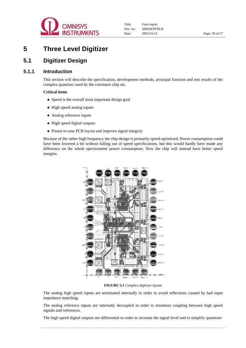
Title: Final reportDoc. no: ABKREPFNLBDate: 2005-03-15 Page: 30 of 57
57
5 Three Level Digitizer
5.1 Digitizer Design
5.1.1 IntroductionThis section will describe the specification, development methods, principal function and test results of thecomplex quantizer used by the correlator chip set.
Critical items
• Speed is the overall most important design goal
• High speed analog inputs
• Analog reference inputs
• High speed digital outputs
• Pinout to ease PCB layout and improve signal integrity
Because of the rather high frequency the chip design is primarily speed-optimized. Power consumption couldhave been lowered a bit without falling out of speed specifications, but this would hardly have made anydifference on the whole spectrometer power consumption. Now the chip will instead have better speedmargins.
FIGURE 5.1 Complex digitizer layout
The analog high speed inputs are terminated internally in order to avoid reflections caused by bad inputimpedance matching.
The analog reference inputs are internally decoupled in order to minimize coupling between high speedsignals and references.
The high speed digital outputs are differential in order to increase the signal level and to simplify quantizer-

Title: Final reportDoc. no: ABKREPFNLBDate: 2005-03-15 Page: 31 of 57
57
to-correlator interface trimming. In a previous design where single ended digital signals were used, trimmingof the decision level in the correlator high speed receiver proved to be tricky. This was because the signaloffset level depends on both quantizer supply voltage and operating temperature.
The pinout is arranged to separate the different interfaces as much as possible. In particular the two analoginput channels are separated from each other as well as from the digital outputs.
5.1.2 PerformanceSimulated performance figures for the complex quantizer together with input requirement are given inTable 5.1.
5.1.3 Technology and Methods The quantizer has been processed by Ericsson Components AB using their P71 bipolar process, revision r2b.The vast majority of transistors used are the 0.6 x 1.5 µm NPNs, with a turnover frequency of about 24 GHz.
The design has been simulated partly and as a whole using Cadence. Layout has been done using Cadencedesign system. The design is solely optimized for speed.
5.1.4 Functional descriptionThe complex quantizer is a dual channel 1.5-bit analog-to-digital converter intended to be used with acomplex correlator in a spectrometer. The architecture of the complex quantizer is shown in Figure 5.2.There are two independent data signal chains, I and Q, with time de-multiplexing factor of two. Each of thesedata chains has one signal input and two reference inputs.
The analogue signal enters on the input pin on the pre-amplifiers. These amplifiers are used for increasedprecision, transforming the indecision of the sampling flip-flop to an acceptable level. The sampling circuitconsists of a simple flip-flop giving a maximum set-up time for the following de-multiplexing stages.
TABLE 5.1 Performance and Specification
Parameter Simulated performance SpecificationMin supply voltage 2.2 V 2.5 V
Current consumption 75 mA TBD
Max supply voltage 2.8 V -
Output rise/fall time 200 ps -
Output swing > 350 mV differential p-p differential
Input frequency 2 GHz 750 MHz
Input dynamic range 1700 mV to Vcc TBD ± 250 mV
Clock frequency 4 GHz 2.2 GHz
Clock swing max. 800 mV differential p-p differential
Clock swing min. 2 mV differential p-p differential
Clock offset range 1700 mV to Vcc-200 mV -
Select signal high min. Vcc-0.1 V -
Select signal low max. Vcc-0.5 V -
S1,S2) Clock division factor = 8, 4, 2, 1
Input sensitivity 100 µV 1 mV
Layout 780 x 1200 µm2 -

Title: Final reportDoc. no: ABKREPFNLBDate: 2005-03-15 Page: 32 of 57
57
FIGURE 5.2 Complex digitizer schematic and layout
The de-multiplexing stages performing the 2:1 time demultiplexing consist of a number of latches with apeculiar clock configuration. The output buffer is a pure differential driver, used for both data and clocksignals.
The clock signal enters the chip differentially and is, after a simple pre-amplifier stage, supplied to aprescaler. This block is programmable by setting the two control bits in one out of four states. The selectabledivide ratios are 1, 2, 4 and 8. The internal clock signal is fed to the samplers and via a divide by two circuitto the de-multiplexor.
Finally the clock is presented to the outside by a, with the data path identical, differential buffer.
In the picture below, the layout of the chip is presented. On the left the quadrature encoded I- and Q signalinputs and the four reference signals are seen, as well as the differential input clock. On the right side of thechip all differential outputs including the clock are seen. Ground is input on each side of the differential inputclock, and Vcc in the upper left corner.
5.2 Digitizer Testing
5.2.1 Digitizer Test setupFigure 5.3 shows the quantizer test board. Power is connected to the right, clock is connected on the upperside of the PCB. On the lower edge of the PCB I- and Q signals are connected. Reference levels are adjustedusing trimming potentiometers.

Title: Final reportDoc. no: ABKREPFNLBDate: 2005-03-15 Page: 33 of 57
57
FIGURE 5.3 Digitizer test set-up.
The actual chip dimensions are 1.2 by 0.8 mm The metal frame around the chip (along the picture frame) isprovided for grounding oscilloscope probes. The vias, which are a bit closer to the chip, are the actual probepoints. The picture also shows that the reference decoupling capacitors (size 0402) are rather far away fromthe chip. If single layer capacitors were used, they could be placed on the bonding pads.
5.2.2 DC characteristics
5.2.2.1 Power consumptionMeasurements have proved the current consumption being independent of clock frequency and input signalsand the total power consumption is between 220-270 mW depending on supply rail.
5.2.3 Digital threshold levelsThe only digital signals on the quantizer are the clock divisor select signals S1 and S2. Table 5.2 andTable 5.3 shows the threshold levels for these control signals. As can be noted, the thresholds are only some0.2-0.3V below the supply voltage. The indecision for these signals are some 20-40 mV.
5.2.4 Comparator threshold versus reference levelsAll measurements below have been performed at room temperature, 2.50V supply voltage, 1GHz samplingclock frequency using a clock division factor of 8.
TABLE 5.2 Clock division control signal thresholds at 2.1V supply voltage
Signal Low threshold (V) High threshold (V)S1 1.92 1.96
S2 1.92 1.96
TABLE 5.3 Clock division control signal thresholds at 2.5V supply voltage
Signal Low threshold (V) High threshold (V)S1 2.24 2.26
S2 2.22 2.26

Title: Final reportDoc. no: ABKREPFNLBDate: 2005-03-15 Page: 34 of 57
57
FIGURE 5.4 Comparator threshold versus reference levels
The conclusion from these tests are that the basic operation is proven.
To test the implications of the indecision and offset levels, the chip set must be operated in a spectrometer.The test here shows that the levels are low, and implications should be removed by the spectrometer signalprocessing.
This was later also proven by the lab testing of the demonstrator, as described in section 8 of this report.
I channel low reference
2.100
2.200
2.300
2.400
2.100 2.200 2.300 2.400
Reference voltage
Thre
shol
d vo
ltage
-0.015
-0.005
0.005
0.015
DC
inde
cisi
on/o
ffset
vol
tage
High thresholdLow thresholdIndecisionOffset
I channel high reference
2.100
2.200
2.300
2.400
2.100 2.200 2.300 2.400
Reference voltage
Thre
shol
d vo
ltage
-0.010
0.000
0.010
DC
inde
cisi
on/o
ffset
vol
tage
High thresholdLow thresholdIndecisionOffset
Q channel low reference
2.100
2.200
2.300
2.400
2.500
2.100 2.200 2.300 2.400 2.500
Reference voltage
Thre
shol
d vo
ltage
-0.015
-0.005
0.005
0.015
DC
inde
cisi
on/o
ffset
vol
tage
High thresholdLow thresholdIndecisionOffset
Q channel high reference
1.900
2.000
2.100
2.200
2.300
2.400
2.500
1.900 2.000 2.100 2.200 2.300 2.400 2.500
Reference voltage
Thre
shol
d vo
ltage
-0.010
0.000
0.010
DC
inde
cisi
on/o
ffset
vol
tage
High thresholdLow thresholdIndecisionOffset

Title: Final reportDoc. no: ABKREPFNLBDate: 2005-03-15 Page: 35 of 57
57
6 Correlator chip(s)
6.1 Correlator Chip Design
6.1.1 IntroductionThis section describes the design, layout and usage of the 128-channel complex correlator chip and a 1024channel chip. Design concepts are identical in both chips, the main difference is the number of channels. The128 channel chip was submitted to foundry in February 2001. The 1024 channel design was submitted tofoundry in March of 2002, and delivered in February 2003. This delay has been the main cause of thechanges in the overall schedule and planning.
This correlator chip can be used in several ways:
• Complex (IQ) auto-correlation, using a time division multiplex factor of two
• Real auto-correlation, using a time division multiplex factor of four
• Dual channel real auto-correlation, using a time division multiplex factor of two
• Real cross-correlation, using a time division multiplex factor of two
However, this section does only describe how to use it when computing complex auto-correlation.
Critical items• Speed is the overall most important design goal• Power consumption• Differential high speed inputs• Integrator length• Data readout scheme• Pinout to ease PCB layout
Because of the rather high frequency the chip design is primarily speed-optimized. Power consumption couldindeed have been lowered a bit without falling out of speed specifications, but this rather small chip wasdesigned to be as fast as possible.
The high speed digital inputs from the quantizer are differential in order to increase these signal levels and tosimplify quantizer-to-correlator interface trimming. In a previous design where single ended digital signalswere used, trimming of the decision level in the correlator high speed receiver proved to be tricky. This wasbecause the signal offset level depends on both quantizer supply voltage and operating temperature.
The integrator length and the clock frequency determines maximum integration time. The number of non-readable bits (prescaler bits) in the integrator can set the signal noise floor higher, if the number of prescalerbits is too large and the input signal noise level is low.
The data readout scheme determines how many I/O-pads that are required. A simple serial interface has beenchosen due to the limited number of pins this requires, and because this will significantly simplify PCBlayout compared to a parallel interface.
The pinout is arranged to separate the different interfaces as much as possible. In particular the high speedinputs are separated from the digital control and readout signals.
6.1.2 Technology and methodsThe correlator is designed for ST Microelectronics HCMOS7 process, version 3.0 (0.25µm CMOS process).
Cadence design tools (Composer, Virtuoso and Analog Artist) have been used throughout the whole designprocess. All design blocks have been simulated in SpectreS. Some blocks have due to complexity reasonsonly been simulated partially.

Title: Final reportDoc. no: ABKREPFNLBDate: 2005-03-15 Page: 36 of 57
57
6.1.3 Functional descriptionFigure 6.1 displays the principle of complex auto-correlation. The quadrature signals I and Q are forwardedto the multipliers, both delayed and non-delayed. The result is then integrated in the summation blocks.
In this correlator chip I and Q data is time multiplexed by a factor of two, in order to improve datathroughput. This makes the correlation blocks a bit more intricate, but the principle remains the same.
FIGURE 6.1 Complex auto-correlation principle
Some details are shown the following subsections. The fine tuning of e.g. clocking and internal databuffering are detailed in the design report.
FIGURE 6.2 Differential input buffer
6.1.4 Inputs from quantizerThe previous correlator chip used a differential input for the clock and pseudo-ECL inputs for quantizer data.This interface required some trimming of the reference level used by the pseudo-ECL inputs and wassomewhat sensitive to temperature and supply voltage variations. Due to these experiences, as well as needfor higher clock rate, a fully differential interface was implemented between the quantizer and the correlatorchip.
The input pads used for the quantizer interface are customized standard analog pads. In these analog padssome metal has been removed to decrease parasitic capacitance, while retaining full protection circuitry. Thisis also compliant with the design rules. Both clock and data inputs use the same differential amplifier/comparator, shown in Figure 6.2.
QQ[n]II[n]QQ[1]II[1]QQ[0]II[0]
Σ
Σ Σ
Σ Σ
Σ Σ
ΣΣ
Σ Σ
Σ
z-1
z-1
z-1
z-1
IQ[0] QI[0] IQ[1] QI[1] IQ[n] QI[n]
Q
I
Inplus Inminus Outplus
Outminus

Title: Final reportDoc. no: ABKREPFNLBDate: 2005-03-15 Page: 37 of 57
57
It is very important that data and clock from the quantizer are equally delayed all the way from the quantizerto the first internal buffering block.
6.1.5 Digital I/OAll digital I/O has been designed using ST Microelectronics standard I/O-cells. All digital inputs are schmitt-triggered to improve noise immunity. Digital I/O is used for serial data readout and correlation control.
6.1.6 Power distributionThe chip has separate power pads for input buffers, correlator core and digital I/O in order to minimize noisein the input circuitry.
The local power lines are designed to have less current density than the design rules allow at maximum chiptemperature. Since the process has as many as six metal layers, two metal layers have been dedicated toglobal power distribution in order to keep the voltage drop across the chip as low as possible.
Local power decoupling capacitors are inserted close to all significant power consumers, i.e. near clockdrivers, data buffers and multipliers. These capacitors and the asynchronous nature of the chip will makesure the supply current spikes are spread in time, thus keeping power supply noise low.
6.1.7 CorrelationThe correlation block is a 1.5 bit multiplier. Since the input signals are limited to values -1, 0 and +1 theresult is also limited to -1, 0 and +1. This makes the multiplier circuit extremely simple.
FIGURE 6.3 Multiplier schematic
The multiplier is optimized for speed, as it runs at full clock speed. Since the “height” of the multiplier layoutcell determines the length of the correlator core, the “height” is squeezed as much as possible.
Figure 6.3 shows the multiplier schematic. As can be seen, it consists of only 9 transistors plus buffers. Whenthe result of the multiplication is positive a pulse is forwarded to the positive integrator and when the result isnegative a pulse is forwarded to the negative integrator. A zero result will cause no output pulse.
6.1.8 IntegrationThe integrator accumulates auto-correlation results. The integrator is divided into two sections: prescaler andreadable integrator. The prescaler is optimized for speed and is running at full clock speed. The readableintegrator is on the other hand optimized for area and is only running at a few MHz at most.
The total number of bits in the integrator is determined by the maximum integration time required and theclock frequency. The number of readable bits is determined by the noise level in the input signal. 31integrator bits, of which 23 can be read, and a clock frequency of 1GHz yields a maximum integration timeof more than one second.
φ
φ
φ
B+ B-
A+ A-
out+
out-
A- A+

Title: Final reportDoc. no: ABKREPFNLBDate: 2005-03-15 Page: 38 of 57
57
Since data from the correlation block is time multiplexed by a factor of two, a lot of area can be saved bydemultiplexing (adding) the data in the integrator, instead of demultiplexing data when reading the data fromthe integrator. This demultiplexing is handled by the Clock joining block.
Figure 6.4 shows how time multiplexing and positive/negative data is handled in the integrator. The twomultipliers to the left in the picture generates the time multiplexed correlation data, which is divided by theprescaler and integrated in the readable integrator.
6.1.9 PrescalerThe prescaler is an 8-bit high speed ripple counter made up of semi-static T-type flip-flops. Only minorchanges has been made since the last correlator chip project.
Figure 6.5 shows the principal schematic of the semi-static T-type flip-flop. A high pulse is generated on theoutput during every second pulse on the input (ø). One important feature of this cell is that the logic state isstable when the input signal is low. This will prevent oscillations that would occur in a fully dynamic cellwhen no input clock is present.
As both input and output signals from the flip-flop are pulses, it is very important that the output pulse isslightly wider than the input pulse. If this was not the case pulses might vanish in the prescaler.
6.1.10 Readable integratorThe readable integrator is a 23-bit low speed ripple counter consisting of static T-type flip-flops. The countercan be reset to zero by holding the /reset signal low.
There is a multiplexed output in this ripple counter, which is used when data is read out. This allows severalintegrators to be read out using a single parallel bus.
6.1.11 Data readoutSince the chip is more or less limited by IO there is a need to minimize the number of pads. A good way ofminimizing the number of IOs is to use a serial bus instead of a parallel bus. The previous correlator chiputilized a total number of 25 data and control signals. This number has been cut down to six pads, of whichthree are used for debugging.
The serial style of reading out data has several advantages:
T
T
T
TTclear
Tclear
T
T
T
TTclear
Tclear
Plus
Minus
Minus
Plus
A0
B0
A1
B1
CORRELATOR
Multiplier Semistatic T-flip/flop
PRESCALER CLOCK JOINING READABLE INTEGRATOR
Static T-flip/flop
Minus
Plus
FIGURE 6.4 Integrator principle schematic
φ
φ
φ
φ
out
FIGURE 6.5 Semi-static T-type flip-flop

Title: Final reportDoc. no: ABKREPFNLBDate: 2005-03-15 Page: 39 of 57
57
• System level design, when only a few signals may need routing between PCBs or boxes
• EMC aspects, when only a few signals need filtering/shielding
• More data bits per integrator don’t require more pads
The only drawback when using a serial interface is the data transfer time, which needs to be investigated ifthe number of correlation lags is increased. The total time for reading out all correlation data, , can befound by using the formula below:
In the formula above 2 is the number of data values per correlation lag, 6 is the number of monitor values(including the dummy monitor) and 24 is the number of bits per data value.
As an example, all data from this 128-channel (128 correlation lags) can be read in about 0.63 milliseconds,when using a 10MHz serial clock.
FIGURE 6.6 128 channel Correlator chip. Die size is 2500 x 3000 um.
6.1.12 128 channel implementationThe correlator core area is 25% smaller than a proportional scaling of the previous chip design; 3.15mm2 vs.33.6mm2/(4*2)=4.2mm2. 4 is the proportional area scaling factor and 2 is the ratio of channels in theprevious chip relative to this. This area reduction has been possible thanks to the real-time time-demultiplexing of data. The serial data readout saves a lot of system level effort when several correlatorchips are used in one instrument.
There are more readable bits in the integrators. This has been possible thanks to serial data readout and real-time time-demultiplexing of data.
The clock speed is improved by 80% compared to specification and is 20-30% faster than expected. Powerconsumption is as expected. Or, the other way around, the power consumption has been allowed to become abit higher than absolute minimum in order to increase the clock frequency.
τ
τ 2 channels 6+⋅( ) 24⋅bitrate
--------------------------------------------------------=

Title: Final reportDoc. no: ABKREPFNLBDate: 2005-03-15 Page: 40 of 57
57
Table 6.1 displays a summary on chip design/simulation results vs. specifications.
6.1.13 1024 channel implementationThe correlator core area is 23% smaller than a proportional scaling of the previous generation chip design;25.8mm2 vs. 33.6mm2*4/4=33.6mm2. Where 4 is the proportional area scaling factor and the ratio ofchannels in this chip relative to the previous generation chip. This area reduction has been possible thanks tothe real-time time-demultiplexing of data.
FIGURE 6.7 1024 channel Correlator chip. Die size is 7000 x 5000 um.
The serial data readout saves a lot of system level effort when several correlator chips are used in oneinstrument. The auxiliary control register may even further ease the system design.
The chip can dynamically be configurated to have 64, 128, 256, 384, 512, 768 or 1024 channels. This may beuseful for conserving power when not all 1024 channels are needed at all times.
The clock speed is improved by 80% compared to specification and is 20-30% faster than expected. Powerconsumption is as expected. Or, the other way around, the power consumption has been allowed to become abit higher than absolute minimum in order to increase the clock frequency.
TABLE 6.1 Comparison specification - simulation/design results
Parameter Specification Simulation/design resultPower consumption per
channel and effective sampling frequency
1mW/GHz ~0.5mW/GHz @ 550MHz clock
Clock frequency 550MHz min. ~1GHz
Area, correlator core - 3.15mm2
Area, with pads - 7.5mm2
Number of channels 64 128, of which 64 can be disabled

Title: Final reportDoc. no: ABKREPFNLBDate: 2005-03-15 Page: 41 of 57
57
Table 6.2 displays a summary on chip design/simulation results vs. specifications.
6.2 Correlator Chip Testing
6.2.1 Test setupFigure 6.8 shows the correlator chip test board for the 1024 channel MCM. A similar board was used for the128 channel MCM.
The test results below is from the 128 channel MCM testing. The 1024 channel tests were completelyconsistent with these results.
FIGURE 6.8 Correlator chip test board
6.2.2 Quiescent power consumptionThe correlator chip has separate supply lines for the input stage (high-speed differential receivers), thecorrelator core and low-speed digital I/O pads, which permits separate power consumption monitoring(correlator core and digital I/O supply are connected to a common pad on the correlator module and have tobe monitored together).
The input stage power consumption is dominated by static currents in the differential amplifiers and is hardlyaffected by changes in data and sampling frequency.
The correlator core is dominated by dynamic power consumption in data buffers and in integrators. Thus it isheavily dependent on both clock frequency and data contents. When data is read out from the chip, someadditional static currents paths are enabled, increasing the power consumption slightly.
TABLE 6.2 Comparison specification - simulation/design results
Parameter Specification Simulation/design resultPower consumption per
channel and effective sampling frequency
1mW/GHz ~0.5mW/GHz @ 550MHz clock
Clock frequency 550MHz min. ~1GHz
Area, correlator core - 25.8mm2
Area, with pads - 35mm2
Number of channels 1024 64, 128, 256, 384, 512, 768 or 1024, depending on
enable signals

Title: Final reportDoc. no: ABKREPFNLBDate: 2005-03-15 Page: 42 of 57
57
FIGURE 6.9 Correlator chip power consumption.
6.2.3 Correlator AC power consumptionFigure 6.9 shows correlator power consumption versus sampling frequency. Furthermore, powerconsumption is displayed for three different input data streams:
• No data (I=Q=0 for all samples)
• Maximum data level (I=+1 or -1, Q=+1 or -1 for all samples)
• Normal data (white noise), (I=0 for 50% of all samples, Q=0 for 50% of all samples)
As can be seen, the power consumption does not fall to 0mW at 0 sampling frequency. This is mainly causedby static current consumption (about 10mA) in the differential receivers. The correlator core/digital I/Ocircuitry adds another 2mA in static power consumption. For a full correlator module it should be noted thatthe quantizer adds another 80mA (200mW).
The power consumption could be said to be roughly:
P = 30 mW + 1 mW / channel / processed GHz,
or as often given
P = 30 mW + 0.5 mW / channel / GHz sampling rate
In addition, there is a small deviation from a straight line in both plots around 1600 MHz. This is themaximum clock rate in this set-up, higher clock rate was late achieved with better cooling of the test board.
6.2.4 Maximum correlation data rateThe maximum correlation data rate (and thus the sampling frequency) depends on the supply voltage. Thechip seems to gain performance with rising supply voltage. However, ST Microelectronics processspecifications suggests that the top performance should be at about 2.5V. Figure 6.10 shows how the
Correlator power consumption versus supply voltage and sampling frequency using 1024 channels, noise input data
0
250
500
750
1000
1250
1500
1750
2000
0 500 1000 1500 2000
Sampling frequency (MHz)
Pow
er c
onsu
mpt
ion
(mW
)
2.67V2.51V2.41V
Correlator power consumption versus data and correlator channels at 2.51V, 1.6GHz sampling frequency
0
250
500
750
1000
1250
1500
1750
2000
2250
2500
0 512 1024
Number of channels enabled
Pow
er c
onsu
mpt
ion
(mW
)
No dataMax dataNoise
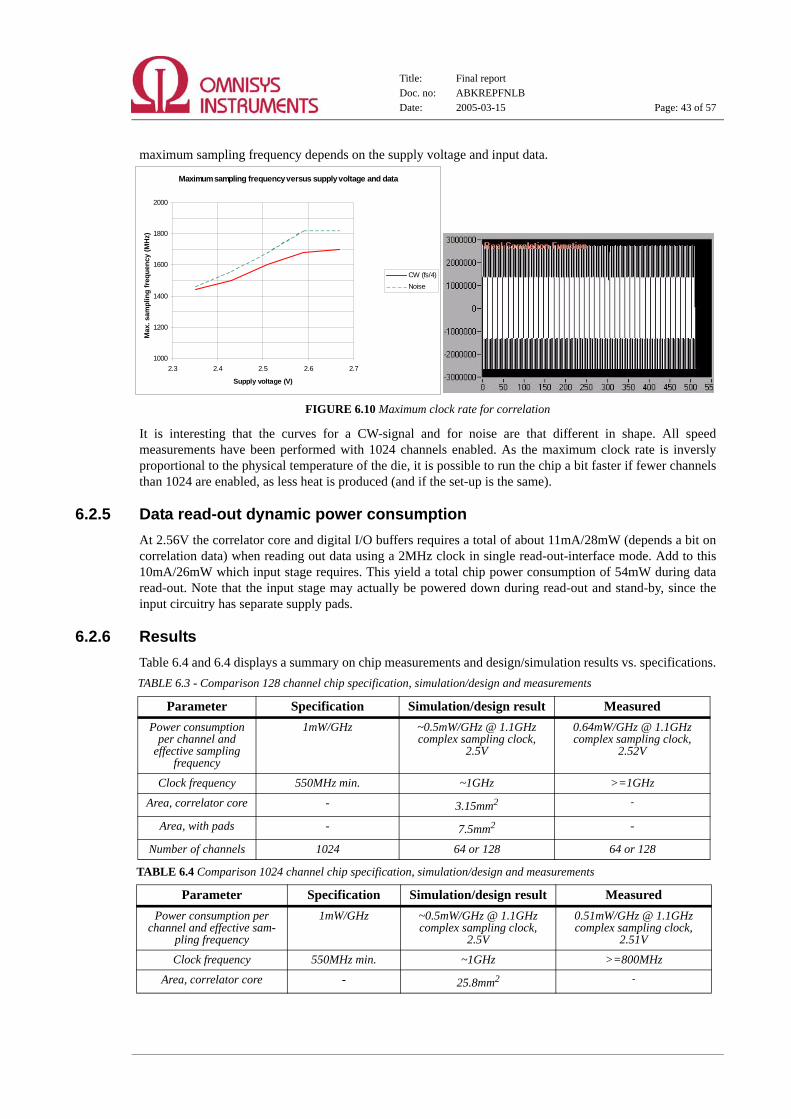
Title: Final reportDoc. no: ABKREPFNLBDate: 2005-03-15 Page: 43 of 57
57
maximum sampling frequency depends on the supply voltage and input data.
FIGURE 6.10 Maximum clock rate for correlation
It is interesting that the curves for a CW-signal and for noise are that different in shape. All speedmeasurements have been performed with 1024 channels enabled. As the maximum clock rate is inverslyproportional to the physical temperature of the die, it is possible to run the chip a bit faster if fewer channelsthan 1024 are enabled, as less heat is produced (and if the set-up is the same).
6.2.5 Data read-out dynamic power consumptionAt 2.56V the correlator core and digital I/O buffers requires a total of about 11mA/28mW (depends a bit oncorrelation data) when reading out data using a 2MHz clock in single read-out-interface mode. Add to this10mA/26mW which input stage requires. This yield a total chip power consumption of 54mW during dataread-out. Note that the input stage may actually be powered down during read-out and stand-by, since theinput circuitry has separate supply pads.
6.2.6 ResultsTable 6.4 and 6.4 displays a summary on chip measurements and design/simulation results vs. specifications.TABLE 6.3 - Comparison 128 channel chip specification, simulation/design and measurements
Parameter Specification Simulation/design result MeasuredPower consumption
per channel and effective sampling
frequency
1mW/GHz ~0.5mW/GHz @ 1.1GHz complex sampling clock,
2.5V
0.64mW/GHz @ 1.1GHz complex sampling clock,
2.52V
Clock frequency 550MHz min. ~1GHz >=1GHz
Area, correlator core - 3.15mm2 -
Area, with pads - 7.5mm2 -
Number of channels 1024 64 or 128 64 or 128
TABLE 6.4 Comparison 1024 channel chip specification, simulation/design and measurements
Parameter Specification Simulation/design result MeasuredPower consumption per
channel and effective sam-pling frequency
1mW/GHz ~0.5mW/GHz @ 1.1GHz complex sampling clock,
2.5V
0.51mW/GHz @ 1.1GHz complex sampling clock,
2.51V
Clock frequency 550MHz min. ~1GHz >=800MHz
Area, correlator core - 25.8mm2 -
Maximum sampling frequency versus supply voltage and data
1000
1200
1400
1600
1800
2000
2.3 2.4 2.5 2.6 2.7
Supply voltage (V)
Max
. sam
plin
g fr
eque
ncy
(MH
z)
CW (fs/4)Noise

Title: Final reportDoc. no: ABKREPFNLBDate: 2005-03-15 Page: 44 of 57
57
6.2.7 ConclusionsThe correlator chip seems to work up to about 1.6GHz complex sampling frequency at nominal supplyvoltage. The measured maximum frequency and power consumption matches the results of the simulationsquite well. The input bandwidth and power consumption is well within the specifications.
The small bug in the read-out control circuitry is of course a bit annoying but is not in any way serious.Another thing worth noticing when building an instrument with this chip is that the read-out interface hasbecome a bit slow; it might take about 3 ms to read out all data from the chip.
Area, with pads - 35mm2 -
Number of channels 1024 64, 128, 256, 384, 512, 768 or 1024
64, 128, 256, 384, 512, 768 or 1024
TABLE 6.4 Comparison 1024 channel chip specification, simulation/design and measurements
Parameter Specification Simulation/design result Measured

Title: Final reportDoc. no: ABKREPFNLBDate: 2005-03-15 Page: 45 of 57
57
7 Radiation tests
7.1 Device under testThe primary devices under test were the full custom bipolar complex quantizer chip (ASCB001B) and thefull custom CMOS 128-channel complex auto correlator chip (ASCB002B). Secondary devices under testwere Analog Devices’ ADF4113BRU PLL frequency synthesizer and Linear Technology’s LT1660CGNoctal DAC.
Figure 7.1 shows the test board which, was used for the radiation test.
FIGURE 7.1 Radiation test board.
The areas marked on the board are:1. Local oscillator (PLL, VCO and crystal oscillator)2. IQ-mixer. (These circuits were removed from the board during the radiation test)3. Correlator chip4. Quantizer chip5. DAC for quantizer reference levels6. Digital control and interface circuitry7. Power supply
To allow for the desired monitoring, a number of current sense resistors were added to the board, which arenot included in the figure.
The original plan was to irradiate only the correlator and quantizer module and the local oscillator. However,it proved to be better to irradiate the full board, to get a more reliable dose rate measure.
7.2 Test setupThe irradiation was performed at Sahlgrenska (University Hospital), using a cobalt-60 source calibrated for adose rate of 412Rad/h, calculated to give about 30kRad over a 3-day test campaign.
Figure 7.2 shows a sketch of the test setup, where the cobalt-60 source radiates the device under test (DUT).A power supply and a CW signal generator provides the necessary signals to the board, while the dataacquisition unit monitors and records voltages and currents. In addition a laptop computer was used for dailybackup of the acquired data.

Title: Final reportDoc. no: ABKREPFNLBDate: 2005-03-15 Page: 46 of 57
57
FIGURE 7.2 Test set-up block diagram.
Figure 7.3 shows the real test setup at Sahlgrenska, where the main parts are marked:• Device under test• Power supply, providing 5V to the test board• Data acquisition unit• CW signal generator, providing the quantizer with a 1GHz sampling clock• Cobalt-60 radiation source, with a dose rate of 412Rad/h
FIGURE 7.3 Test set-up.
7.3 Monitored signalsThe following signals were monitored by the data acquisition unit:
• supply voltages• quantizer supply current• correlator core and input circuitry supply currents• PLL core and digital I/O supply currents• VCO supply current• frequency synthesizer feedback loop filter OPAMP supply current• DAC, DAC reference and reference OPAMP supply current• 7 digital outputs from the on-board micro controller• ambient temperature

Title: Final reportDoc. no: ABKREPFNLBDate: 2005-03-15 Page: 47 of 57
57
7.4 Test procedureThe on-board micro controller was programmed to repeatedly do the following tests:
• check the PLLs lock detect signal, by forcing it high and low
• check that the PLL doesn’t report successful locking outside the VCOs frequency range
• check that the PLL reports successful locking at the nominal LO frequency
• correlate one second each at 1GHz, 500MHz, 250MHz and 125MHz sampling frequency, using four different data patterns, checking that the resulting monitor and correlation data is correct
• correlate 95 seconds at 1GHz for each of three different data patterns, so the current consumption can be monitored
After the full 74 hours of irradiation (31kRad), the devices and instruments were moved back to Omnisyslab, where the failed micro controller was replaced and annealing was performed, with the same monitoringand software running as in the beginning of the irradiation period.
7.5 ResultsIn conclusion, the correlator MCM complied with specification after 31 kRAD radiation. For both thecorrelator chip (CMOS) and digitizer (Bipolar), the changes in power consumption was negligible.

Title: Final reportDoc. no: ABKREPFNLBDate: 2005-03-15 Page: 48 of 57
57
8. The 6 GHz Spectrometer Demonstrator
8.1 Demonstrator DesignThe spectrometer demonstrator is contained in a dual compartment aluminium box. It consists of threeprinted circuit boards; the intermediate frequency signal distribution board (IF), the quadrature mixing board(IQ) and the correlator board (CCM).
General test results:
• weight: 0.74kg
• supply voltage: single +5V
• power consumption: 6.2W
• input frequency range: 0.65GHz - 6.65 GHz (6GHz simultaneous bandwidth)
• frequency resolution: 13MHz/channel
These are between a factor of 3-10 better than specified for the demonstrator input specification, and there iseven room for improvements.
As can be seen in Figure 8.2 and Figure 8.3, there is still much space in the box. The demonstrator can befitted with a second IQ board and a redesigned CCM board with eight correlator chips, yielding asimultaneous processing bandwidth of 12GHz. The power consumption would then be about 10 W and theweight less than 1kg.
The demonstrator is based on the design shown in Figure 8.1.
FIGURE 8.1 Demonstrator design
The design is based on a frequency multiplexed architecture, with four sub-bands covering 1.5 GHz each.The chip set implements time multiplexing, so that the complete spectrometer actually use both time and
0 .5 -7 G H z(T B D )
In te rface
syn th
w h ite no ise s ou rce
cw s ig na l
P W R m o d u le
C o n tro l N o teb o o kL ab v ie wM a tla b
R S -2 32 (T B D )
12 8 ch ,co m p lex
c o rre la to r A S IC
II
Q
H y b
Q
II
Q
Q
1 2 8 ch ,co m p le x
co rre la to r A S IC
C o n tro l lo g icL ab te s t se t-up
P W R su p p ly
1 .5 G H z
H y b
1 2 8 ch ,co m p le x
co rre la to r A S IC
II
Q
H yb
Q
II
Q
Q
1 2 8 ch ,co m p le x
co rre la to r A S IC
3 .0 G H z
H yb
4 .5 G H z7 .5 G H z
0 .7 5 -2 .2 5 G H z
2 .2 5 -3 .7 5 G H z
3 .7 5 -5 .2 5 G H z
5 .2 5 -6 .7 5 G H z
0 .7 5 -6 .75 G H z
3 .75 -6 .75 G H z

Title: Final reportDoc. no: ABKREPFNLBDate: 2005-03-15 Page: 49 of 57
57
frequency multiplexing.
The demonstrator consist mainly of one IF processing section, one IQ converter section and one CorrelatorModule section. This has been designed to be housed in one mechanical box of 170x110x30 mm size, withroom for expansion to a 12 GHz spectrometer. This implies a duplication of most of the electronics.
FIGURE 8.2 Correlator PCB.
Some of the main functions housed on the correlator PCB are:• micro controller, crystal oscillator and interface circuits• sampling clock generator (VCO, PLL, filter and voltage regulators)• correlator support circuits (DACs and voltage regulators)• correlator modules
FIGURE 8.3 IF electronics.
Some of the main functions housed on the IF electronics are:• local oscillators for the IQ mixers (VCOs, PLLs, filters and voltage regulators)• IQ mixers (90-degree hybrids and mixers)• amplifiers
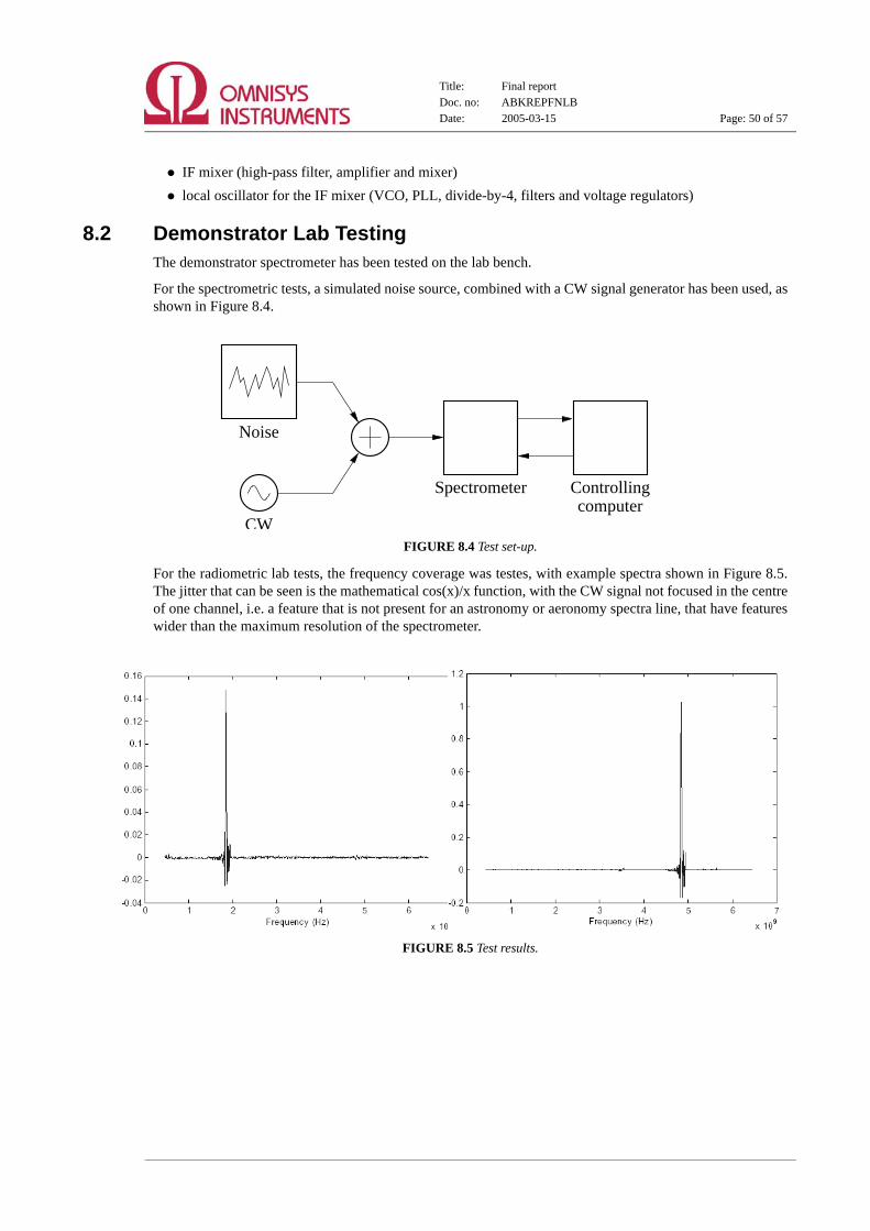
Title: Final reportDoc. no: ABKREPFNLBDate: 2005-03-15 Page: 50 of 57
57
• IF mixer (high-pass filter, amplifier and mixer)• local oscillator for the IF mixer (VCO, PLL, divide-by-4, filters and voltage regulators)
8.2 Demonstrator Lab TestingThe demonstrator spectrometer has been tested on the lab bench.
For the spectrometric tests, a simulated noise source, combined with a CW signal generator has been used, asshown in Figure 8.4.
FIGURE 8.4 Test set-up.
For the radiometric lab tests, the frequency coverage was testes, with example spectra shown in Figure 8.5.The jitter that can be seen is the mathematical cos(x)/x function, with the CW signal not focused in the centreof one channel, i.e. a feature that is not present for an astronomy or aeronomy spectra line, that have featureswider than the maximum resolution of the spectrometer.
FIGURE 8.5 Test results.
Noise
CW
Spectrometer Controllingcomputer

Title: Final reportDoc. no: ABKREPFNLBDate: 2005-03-15 Page: 51 of 57
57
9 Radiometer Test Results
9.1 IntroductionThe demonstration spectrometer has been tested in parallel with an AOS in a 110 GHz radiometer set-up atthe University of Bremen.
The microwave radiometer BRERAM (BREmen Radiometer for Atmospheric Measurements) wasdeveloped for monitoring the vertical profiles of stratospheric ozone over Bremen.
Despite its small concentration, the atmospheric trace gas ozone (O3) is an important component of theatmosphere. On the one hand ozone absorbs the UV-B radiation which is harmful for the biosphere. On theother hand it contributes to the energy budget of the planet Earth, and determines the temperature structure ofthe stratosphere.
A microwave Radiometer (MR) is well suited to continuously monitor stratospheric composition since MRoffer the possibility to measure ozone profiles continuously, day and night, and are only little affected bymeteorological conditions. Furthermore a MR can be accurately calibrated by using reference radiators, so-called “Black Bodies” at various temperatures.
The output data has been compared by both Omnisys and a research group at Bremen. A short description ofthe test set-up and the results follow.
FIGURE 9.1 BRERAM radiometer.
9.2 Radiometer overviewThe radiometer system consists of a quasi-optical processing subsystem, followed by a first downconversionstage. These two functions translate the sky signal of 110.8 GHz down to an intermediate frequency, centredaround 8 GHz. This is often described as the “front-end” of a radiometer.
After this, a further donwconversion follows, complemented with amplifiers, before AOS (Acousto OpticalSpectrometer) signal processing. This is the back-end of the radiometer.
To operate the front-end and back-end, there is a need for a computer, power supplies and some additionalcontrol and telemetry electronics.

Title: Final reportDoc. no: ABKREPFNLBDate: 2005-03-15 Page: 52 of 57
57
The complete assembly, can be seen in Figure 9.1.
FIGURE 9.2 Block diagram of the radiometer set-up the University of Bremen.
9.3 Front-end detailsThe atmospheric signal enters the laboratory through a Styrofoam window which is transparent formicrowaves. The first element in the front-end is a rotatable mirror by which the observation angle can bevaried over an elevation range from 15 to 45 degrees. Measurements are performed in the total power mode,i. e. the mirror points in regular intervals at hot and cold calibration loads (Black Bodies), and under a presetangle at the sky. The calibration loads consist of microwave absorber material which can be considered as ablack body emitter in the microwave region of the spectrum. The hot load is at room temperature (about296K and the cold load is submerged into liquid Nitrogen with a temperature of about 77K.
Next we have the quasi optics; the signal beam is linearly polarized by a wire grid. The following ellipticalmirrors are focussing the beam through all quasi optical elements to the horn antenna of the first mixer at110GHz. In addition the optics contains an interferometer (Martin Puplett interferometer) used as single sideband filter to suppress the unwanted image side band. Furthermore a path length modulator is used to reducestanding waves between the horn antenna and all quasi optical elements.
A rather large technical problem arises due to multiple reflections of the electromagnetic wave inside thequasi optics: Parallel plane surfaces will form a Fabry-Perot-Interferometer, which leads to a modulation ofthe pass band. The suppression of such undesired effects is done by the so-called path length modulator. Thepath length modulator (PLM) consists of a wire grid where the incoming linear polarized beam is totallyreflected and directed on to a rooftop mirror which turns the polarization by 90 degrees. The reflected beamwill transmit the grid and leave the PLM through the output port. The rooftop mirror is periodically movedback and forth, this will change the pathlength of the whole quasi optics, and consequently also change the
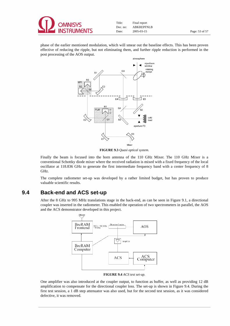
Title: Final reportDoc. no: ABKREPFNLBDate: 2005-03-15 Page: 53 of 57
57
phase of the earlier mentioned modulation, which will smear out the baseline effects. This has been proveneffective of reducing the ripple, but not eliminating them, and further ripple reduction is performed in thepost processing of the AOS output.
FIGURE 9.3 Quasi optical system.
Finally the beam is focused into the horn antenna of the 110 GHz Mixer. The 110 GHz Mixer is aconventional Schottky diode mixer where the received radiation is mixed with a fixed frequency of the localoscillator at 118.836 GHz to generate the first intermediate frequency band with a center frequency of 8GHz.
The complete radiometer set-up was developed by a rather limited budget, but has proven to producevaluable scientific results.
9.4 Back-end and ACS set-upAfter the 8 GHz to 995 MHz translations stage in the back-end, as can be seen in Figure 9.1, a directionalcoupler was inserted in the radiometer. This enabled the operation of two spectrometers in parallel, the AOSand the ACS demonstrator developed in this project.
FIGURE 9.4 ACS test set-up.
One amplifier was also introduced at the coupler output, to function as buffer, as well as providing 12 dBamplification to compensate for the directional coupler loss. The set-up is shown in Figure 9.4. During thefirst test session, a 1 dB step attenuator was also used, but for the second test session, as it was considereddefective, it was removed.

Title: Final reportDoc. no: ABKREPFNLBDate: 2005-03-15 Page: 54 of 57
57
It should be noted that the AOS set-up has been used and debugged for several years, while the ACS systemintegration is more ad-hoc. The main difference between the two spectrometers is that the ACS has about 13MHz resolution, while the AOS has about 1 MHz.
9.5 Test results, analyses and discussionThe ACS was operated during the first test session as a piggy-back during normal observations for twomonths. In addition, some complementary tests were made several months later at a second test session.Standard practical problems were the operation as well as the control and data processing of the output data,as two different computers was used. This was with software developed at several years apart, by differentorganisations, processing data from two different types of spectrometers. The results still proved the functionand performance of the ACS, but some debugging of the set-up was necessary.
FIGURE 9.5 Spectra taken against a reference load. The frequency axis is not the sky frequency.
In Figure 9.5, the raw spectra from observing the calibration load are shown, and in Figure 9.6 and 9.7, skyspectra with the ozone line are displayed. The ACS spectra are shown without any post processing, while theAOS spectra are convoluted with the response function of the ACS. The basic response of the ACS is a sincfunction, and it effectively reduces the resolution of the AOS spectra from 1 MHz down to 7 MHz.
The real test of spectrometers are linearity and overall shape of the processed spectra. The linearity can betested in the lab, as shown in an earlier chapter of this report, while the shape is best tested with a truespectrum. Observation of a spectrum also shows linearity and off-set type of effects.
The plots show results from two different data sets, taken 15 minutes apart, resulting in a 17 K differencebetween the sets. In this plot, we can se that there is no offset between the AOS and ACS spectra.Furthermore, we can see that there is neither a linearity deviation, nor an overall shape disagreement.

Title: Final reportDoc. no: ABKREPFNLBDate: 2005-03-15 Page: 55 of 57
57
FIGURE 9.6 Two sets of AOS and ACS spectra. Frequency axis is on the sky and GHz. Four spectra are shown, two ACS spectra and two AOS spectra. On the top, we have the AOS plot in blue and the ACS plot in red. On the bottom, we have
the AOS plot in light blue and the ACS plot in green.
FIGURE 9.7 Another two sets of AOS and ACS spectra. Frequency axis is on the sky and GHz. Four spectra are shown, two ACS spectra and two AOS spectra. On the top, we have the AOS plot in blue and the ACS plot in green. On the
bottom, we have the AOS plot in light blue and the ACS plot in red.

Title: Final reportDoc. no: ABKREPFNLBDate: 2005-03-15 Page: 56 of 57
57
We have a number of observations from these spectra. These are primarily:
• the overall shape is very similar for the two spectrometers, i.e. both the peak and the slope over the spectra
• the linearity agrees
• there is no, or very little off-set between the AOS and ACS signal spectra
• a large interference peak in both AOS and ACS spectra close to 111.1 GHz
The large peak originates from one commercial RF transmitter in the Bremen area.
However, there are also a few deviations. These can originate from either the AOS or the ACS, but as theAOS is an operational instrument and the ACS is an early prototype in an ad-hoc set-up, it is expected thatthe ACS cause these deviations. These are:
• the response to the peak is different
• we have noted a small offset of around 1K between some ACS and AOS spectra (see lower part of fig. 9.5)
• we have a peak at 110.6 GHz in the ACS spectra but not in the AOS one.
Possibly, the fact of having a single converter (quantiser) for the whole spectrum could affect sensitivity orintroduce a slight offset, when this quantiser is saturated by the presence of a strong interferer..
The left peak is caused by the ACS IQ mixer topology used in this particular ACS, used to translate the IFinput signal down to DC baseband for the correlator to process. The LO for the IQ mixer is at 1.5 GHz(translated through the IF system to 110.6 GHz sky frequency) and the bump is the result of low frequencyEMC disturbance.
In the set-up, the DC power supply wires were not shielded, and the RF environment was not controlled atall. This particular ACS is a low cost demonstrator and based on experience, one more design iteration wouldcertainly remove this problem. A response on the IF-DC frequency is a common occurrence in the earlyprototyping phase of ACS spectrometers.
The small ripple effect (?) that can be seen in the spectra has not been fully explained. At the initial tests,Omnisys were informed that this could originate from quasi-optical ripple, but this explanation has later beenquestioned by Bremen. However some testing in this respect was performed. The LO was shifted infrequency and the bumps did not shift in the final spectra. This shows that they originate from outside theACS. The same effect can be seen in Figure 9.6 and 9.7, with different data sets, but not in the calibrationload spectra, Figure 9.5.
The most plausible explanation now is a ripple (reflections) in the temporary IF interface to the ACS,originating from a defective attenuator used in the set-up. This was not used for the calibration load tests thatwas taken at the second test session (Figure 9.5), and the ripple disappears in these spectra. The attenuatorwas determined defective after lab testing at Omnisys between the two sessions at Bremen.
The initial efforts to get the tests going were straightforward. However, the test procedures planned were notclear from both sides and there were also data format problems when comparing the AOS and ACS data.This made the interpretation harder of the unexpected deviations. After a few weeks, it was clear that therewas a time extraction error in the Matlab code used and the wrong AOS and ACS spectra were compared.
Overall, the ACS showed a performance that was compliant with the scientist expectations, and it wasclearly recognised that the small deviations shown could be expected in such a test set-up. The scientists atBremen declared their interest in a high resolution ACS to complement the AOS, and asked for costestimates for custom wide band implementations.
The performance issues seen in the comparison between the AOS and ACS are expected. The AOS haveseveral years of debugging and improvements behind it, while the ACS had a few weeks of lab tests atOmnisys, and just a few hours of debugging of the set-up at Bremen.

Title: Final reportDoc. no: ABKREPFNLBDate: 2005-03-15 Page: 57 of 57
57
10 Conclusion and future prospectsThis report describes a spectrometer implemented in Multi Chip Module technology. The function andperformance has been demonstrated in lab tests, as well as by operating a full demonstrator spectrometer in aground based 110 GHz radiometer. There were two MCM’s produced, based on two different correlatorchips.
The specification was 1 GHz bandwidth with 64 and 1024 spectral channels respectively, and with a powerconsumption of less than 1 mW/GHz/channel. The result is 1.7 GHz bandwidth, 128 and 1024 channelsresolution, and 0.5 mW/GHz/channel power consumption.
Major items for spectrometers are of course bandwidth and system integration level, but for spaceapplications, the power consumption is also vital. In this aspect, the chip set developed in this project is 23times better than the competition.
To demonstrate the capabilities, a demonstrator has been designed and tested. The specification for thedemonstrator has followed the Master/Marschal requirements, with 20 W power consumption and 10 kgmass. The demonstrator has shown that the performance can be realised with a system of less than 1 kg andless than 8 W power consumption. With flight development, this could be reduced to 4-5 W and 400 grams.The demonstrator has been proven to have a performance that match an AOS that is used by earthobservation scientist at the University of Bremen.
Now, as a result from the development at Omnisys described in this report, a general conclusion is thatautocorrelation spectrometers are very competitive with other type of spectrometers for space and groundbased (sub)millimeter radiometry. The main advantages are: compact implementations, scalability andversatility in bandwidth and resolution, combined with potentially very high stability. There are no known, orproven disadvantages.
In terms of size and mass, the correlator is clearly much more compact than either the Chirp or the AOS, anoptimised CTS being 2-3 times the size of a correlator, while an AOS is at least 10 times larger.
In terms of power consumption, the CTS is comparable to the ACS for narrow bandwidth, while the AOSconsumes 2-4 times more than the ACS for wide bandwidth applications. The CTS can not compete for widebandwidth applications, while the AOS is not competitive for high resolution use.
In terms of flexibility in bandwidth and resolution, the CTS and the AOS have very limited capabilities.
The ACS uses no special technologies and components, such as lasers, CCD's, Bragg Cell's or Chirp filters,with concerns regarding availability, radiation tolerance and other quality concerns. The only specialtechnology is the full custom design of the chip set, while a $1000 Billion industry helping in the productionline set-up. The NRE for the ASIC's are about $100-150 K.
There is a need for spectrometers for space based radiometers with between 4-10 GHz bandwidth in the nextyears to come. The best candidate to meet these requirements is the ACS, but additional development isneeded. Omnisys has performed a design study, with the conclusion that it is clearly possible to develop atrue single chip spectrometers with 4-6 GHz bandwidth and up 2000 channels. This would be a single chipspectrometer, including a large part of the IF processing. Based on this experience, it should be possible toachieve 10-15 GHz bandwidth within 3-5 years time, still with impressive size and power consumptionfigures.
The 4 GHz+ spectrometer chip would have a number of obvious applications. It would benefit most groundbased and space borne aeronomy radiometers, as well as space science instruments.