ti tms320c55x ver2.0 - aalborg...
TRANSCRIPT
Revision: 2.0 TI TMS320C55x Platform Pages: 21
3G DSP "Mål2" Project, Aalborg University - 1 -
TI TMS320C55x Platform
Contents
1 Document Objectives ............................................................................. 32 Processor Description ............................................................................ 3
2.1 Architecture........................................................................................................ 32.2 Memory system.................................................................................................. 5
2.2.1 Physical Memory Layout ...........................................................................52.2.2 Logical Memory Layout .............................................................................52.2.3 Instruction Cache ......................................................................................5
2.3 Register Model................................................................................................... 62.4 Functional Units ................................................................................................. 7
2.4.1 Instruction Buffer Unit (IBU).......................................................................72.4.2 Program Flow Unit (PFU) ..........................................................................72.4.3 Address-data Flow Unit (AFU)...................................................................82.4.4 Data Computation Unit ..............................................................................8
2.5 Pipeline.............................................................................................................. 82.5.1 Pipeline Stages .........................................................................................82.5.2 Branching..................................................................................................92.5.3 Data Conflicts............................................................................................9
2.6 Instruction set .................................................................................................. 102.6.1 Absolute Addressing Mode......................................................................112.6.2 Direct Addressing Mode ..........................................................................112.6.3 Indirect Addressing Mode........................................................................112.6.4 Instruction Set Orthogonality ...................................................................12
2.7 Hardware Modes.............................................................................................. 122.8 Programming Model......................................................................................... 13
2.8.1 Assembly Language Format....................................................................132.8.2 Efficient Code: Use All Resources All the Time........................................13
3 Compiler............................................................................................... 143.1 Options/Which Optimizations?.......................................................................... 14
3.1.1 Optimization levels ..................................................................................143.2 Language Implementation................................................................................ 16
3.2.1 Data Types..............................................................................................163.2.2 Right Shift Operator.................................................................................17
3.3 Language Extensions / Pragmas / Intrinsics ..................................................... 173.3.1 Pragmas .................................................................................................173.3.2 Intrinsics..................................................................................................173.3.3 Inline Assembly.......................................................................................17
3.4 Run Time Environment..................................................................................... 183.4.1 Memory Model ........................................................................................183.4.2 Register Conventions ..............................................................................183.4.3 Calling Conventions ................................................................................19
Revision: 2.0 TI TMS320C55x Platform Pages: 21
3G DSP "Mål2" Project, Aalborg University - 2 -
3.5 Optimization Strategy....................................................................................... 19
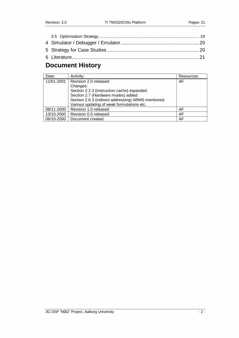
4 Simulator / Debugger / Emulator.......................................................... 205 Strategy for Case Studies .................................................................... 206 Literature.............................................................................................. 21
Document HistoryDate: Activity: Resources:11/01-2001 Revision 2.0 released
Changes:Section 2.2.3 (instruction cache) expanded.Section 2.7 (Hardware modes) added.Section 2.6.3 (indirect addressing) ARMS mentioned.Various updating of weak formulations etc.
AF
08/11-2000 Revision 1.0 released AF13/10-2000 Revision 0.5 released AF06/10-2000 Document created. AF
Revision: 2.0 TI TMS320C55x Platform Pages: 21
3G DSP "Mål2" Project, Aalborg University - 3 -
1 Document Objectives
The objective of this document is to present a description and analysis of theTMS320C55x processor and it's associated set of tools.
This document is based on [TI, 2000a] [TI, 2000b] [TI, 2000c] [TI, 2000d].
2 Processor DescriptionThe TMS320C55x (hereafter C55x) is a multi-issue fixed point processor which operatesprimarily on 16 bit data. It is the successor to the TMS320C54x family and is backwardassembly source code compatible with C54x devices. The intended use of the C55xprocessor family is applications that are DSP intensive, low cost (requires low memoryusage), and require high power efficiency such as cell phones, digital cameras, andportable audio players. The first commercially available processor in the C55x family isthe C5510 for which samples running 160 MHz were available September 2000.According to TI, the processor should scale well beyond 200 MHz [TI, 2000a].
2.1 Architecture
The C55x architecture has its roots in an enhanced conventional DSP architecture. Asconventional DSP architectures, it is based on a modified Harvard architecture withseveral independent data- and program busses, data address generation units, zerooverhead looping capabilities, and support for circular buffers [Lapsley, 1996]. Thefollowing features characterize the C55x processor when compared with conventionalDSP architectures:
• 5 unidirectional 16-bit data busses: 3 for data read and 2 for data write.• Dual MAC• Viterbi support: Hardware supported Viterbi decoding• Multi-issue: Executes up to two instructions in parallel.• Variable instruction width: Instruction word width vary between 8 and 48 bit, leading
to smaller overall memory usage (hopefully!).
All parallelism must be detected and scheduled at compile-time, i.e. there is no hardwarebased scheduling of instructions as in a superscalar architecture. The operations percycle efficiency is obtained as a mix of encoding of multiple operations into instructionsand the execution of multiple instructions in parallel. The former is characteristic forenhanced conventional DSP processors (e.g. the Lucent DSP16210) whereas the later ischaracteristic for VLIW DSP processors (e.g. the TI TMS320C6201), so it is debatablewhether this DSP should be characterized as an enhanced conventional DSP. Thisfollows the industry design trend, where the distinction between classes of processorsgets more blurred every time a new DSP architecture is announced (e.g. the AnalogDevices TigerSHARC architecture, or the TI TMS320C64x architecture, which bothcombine SIMD and VLIW methods of obtaining increased parallelism).
A block diagram of the C55x architecture is shown on Figure 1.

Revision: 2.0 TI TMS320C55x Platform Pages: 21
3G DSP "Mål2" Project, Aalborg University - 4 -
Figure 1 Block Diagram of the C55x CPU [TI, 2000b, p.1-2].
On the figure, the read busses are shown above the CPU and the data-write busses areshown below the CPU. As indicated by the width of the address busses, the C55x CPUcan address 16 Mbyte memory (24-bit addresses). The maximum memory bandwidth is:
• 32 bit / cycle for instruction read• Three 16-bit words / cycle for data read• Two 16-bit words / cycle for data write
In section 2.2 a closer look at the memory system is presented. The CPU contains 4functional units: An instruction buffer unit, a program flow unit, an address-data flow unit,and a data computation unit. Furthermore the external memory interface unit is shown.Three of the units are connected to the C and D data read busses, whereas only the datacomputation unit are connected to the B data read bus. The B data read bus can onlyaccess internal memory. The figure also shows that all the data addresses (both read-and write accesses) are generated by the address data-flow unit, whereas all programaddresses are generated by the program flow unit and all instructions are received by theinstruction buffer unit. The C55x is not a load-store architecture, and functional units canoperate on data directly from memory.
Revision: 2.0 TI TMS320C55x Platform Pages: 21
3G DSP "Mål2" Project, Aalborg University - 5 -
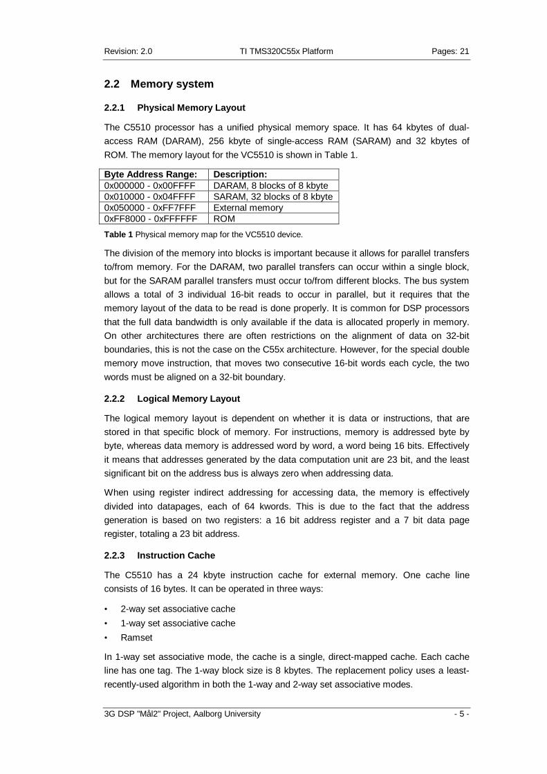
2.2 Memory system
2.2.1 Physical Memory Layout
The C5510 processor has a unified physical memory space. It has 64 kbytes of dual-access RAM (DARAM), 256 kbyte of single-access RAM (SARAM) and 32 kbytes ofROM. The memory layout for the VC5510 is shown in Table 1.
Byte Address Range: Description:0x000000 - 0x00FFFF DARAM, 8 blocks of 8 kbyte0x010000 - 0x04FFFF SARAM, 32 blocks of 8 kbyte0x050000 - 0xFF7FFF External memory0xFF8000 - 0xFFFFFF ROM
Table 1 Physical memory map for the VC5510 device.
The division of the memory into blocks is important because it allows for parallel transfersto/from memory. For the DARAM, two parallel transfers can occur within a single block,but for the SARAM parallel transfers must occur to/from different blocks. The bus systemallows a total of 3 individual 16-bit reads to occur in parallel, but it requires that thememory layout of the data to be read is done properly. It is common for DSP processorsthat the full data bandwidth is only available if the data is allocated properly in memory.On other architectures there are often restrictions on the alignment of data on 32-bitboundaries, this is not the case on the C55x architecture. However, for the special doublememory move instruction, that moves two consecutive 16-bit words each cycle, the twowords must be aligned on a 32-bit boundary.
2.2.2 Logical Memory Layout
The logical memory layout is dependent on whether it is data or instructions, that arestored in that specific block of memory. For instructions, memory is addressed byte bybyte, whereas data memory is addressed word by word, a word being 16 bits. Effectivelyit means that addresses generated by the data computation unit are 23 bit, and the leastsignificant bit on the address bus is always zero when addressing data.
When using register indirect addressing for accessing data, the memory is effectivelydivided into datapages, each of 64 kwords. This is due to the fact that the addressgeneration is based on two registers: a 16 bit address register and a 7 bit data pageregister, totaling a 23 bit address.
2.2.3 Instruction Cache
The C5510 has a 24 kbyte instruction cache for external memory. One cache lineconsists of 16 bytes. It can be operated in three ways:
• 2-way set associative cache• 1-way set associative cache• Ramset
In 1-way set associative mode, the cache is a single, direct-mapped cache. Each cacheline has one tag. The 1-way block size is 8 kbytes. The replacement policy uses a least-recently-used algorithm in both the 1-way and 2-way set associative modes.
Revision: 2.0 TI TMS320C55x Platform Pages: 21
3G DSP "Mål2" Project, Aalborg University - 6 -
In 2-way set associative mode, the cache is structured similar to two arrays of direct-mapped cache. Each cache line has two tags. The two-way block size is 16 kbytes.
In Ramset mode, the value of the tag is fixed and for each tag there is an array of 256cache lines, i.e., the block size is 4 kbytes. In this mode cache lines are not replacedunless the tag is changed or the cache is flushed.
According to TI, the Ramset mode provides better cache performance for frequently usedlinear blocks of code that will fit within the 4 kbyte block size. The 2-way and 1-way setassociative modes provide more efficient cache performance that does not execute in alinear stream (branching code or calls/returns).
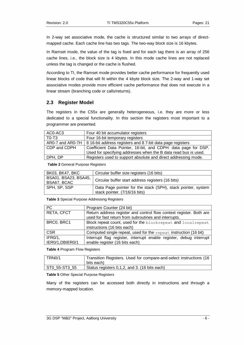
2.3 Register Model
The registers in the C55x are generally heterogeneous, i.e. they are more or lessdedicated to a special functionality. In this section the registers most important to aprogrammer are presented.
AC0-AC3 Four 40 bit accumulator registersT0-T3 Four 16-bit temporary registersAR0-7 and AR0-7H 8 16-bit address registers and 8 7-bit data page registersCDP and CDPH Coefficient Data Pointer, 16-bit, and CDPH: data page for DSP.
Used for specifying addresses when the B data read bus is used.DPH, DP Registers used to support absolute and direct addressing mode.
Table 2 General Purpose Registers
BK03, BK47, BKC Circular buffer size registers (16 bits)BSA01, BSA23, BSA45,BSA67, BCAC Circular buffer start address registers (16 bits)
SPH, SP, SSP Data Page pointer for the stack (SPH), stack pointer, systemstack pointer. (7/16/16 bits)
Table 3 Special Purpose Addressing Registers
PC Program Counter (24 bit)RETA, CFCT Return address register and control flow context register. Both are
used for fast return from subroutines and interrupts.BRC0, BRC1 Block repeat count, used for the blockrepeat and localrepeat
instructions (16 bits each)CSR Computed single repeat, used for the repeat instruction (16 bit)IFR0/1,IER0/1,DBIER0/1
Interrupt flag register, interrupt enable register, debug interruptenable register (16 bits each)
Table 4 Program Flow Registers
TRN0/1 Transition Registers. Used for compare-and-select instructions (16bits each)
ST0_55-ST3_55 Status registers 0,1,2, and 3. (16 bits each)
Table 5 Other Special Purpose Registers
Many of the registers can be accessed both directly in instructions and through amemory-mapped location.

Revision: 2.0 TI TMS320C55x Platform Pages: 21
3G DSP "Mål2" Project, Aalborg University - 7 -
As evident from the tables, there are many registers dedicated to a special functionality.The general-purpose registers are also divided into data registers and address registers,i.e., the register file is generally heterogeneous.
2.4 Functional Units
In the following each functional unit is described.
2.4.1 Instruction Buffer Unit (IBU)
The instruction buffer unit has two functions: It has an instruction queue and aninstruction decoder.
The instruction queue acts as a small cache, that ensures that the next instruction to beexecuted is always ready. It is necessary because the memory bandwidth for instructionread is 4 bytes / cycle, and instruction packets are up to 6 bytes. (An instruction packetbeing one instruction or two instructions if they are to be executed in parallel). I.e. whenissuing instruction packets larger than 4 bytes, the IBU cache is drained, and whenissuing instruction packets smaller than 4 bytes, the IBU cache gets preloaded. Thecache can contain 64 byte of undecoded instructions. Besides ensuring that the pipelineis kept full, the small cache has two other advantages:
• A block of instructions that is repeated can execute from the IBU cache, reducingpower consumption by eliminating memory reads (through a dedicatedlocalrepeat instruction)
• Instructions can be speculatively preloaded for conditional branch, call, and returninstructions
Furthermore decoding of instructions are performed in the IBU before they are issued tothe other function units. First of all, the instruction boundaries are identified, and secondlyconstants encoded in the instructions are isolated and forwarded to the relevant functionunits.
2.4.2 Program Flow Unit (PFU)
The program flow unit generates all program addresses, and controls the sequence ofinstructions. The program-address generation generates 24-bit addresses, normally in asequential manner. The PFU also contains control logic, that handles the following tasks:
• Three levels of hardware supported zero-overhead looping (two levels of variablesize of blocks and one level with only one instruction in the loop body)
• Evaluation of conditions for conditional instructions• Initialize interrupt servicing• Determine the branch address for the special switch instruction
The PFU contains registers to support program flow, block-repeat and single-repeat ofinstructions, interrupt control, and status registers.
Revision: 2.0 TI TMS320C55x Platform Pages: 21
3G DSP "Mål2" Project, Aalborg University - 8 -
2.4.3 Address-data Flow Unit (AFU)
The address data flow unit contains the logic (data address generation: DAGEN) and theregisters necessary to handle the generation of data-space addresses. Furthermore itcontains a 16-bit ALU that can perform arithmetical, logical, shift and saturationoperations. The ALU saturation mode is affected by a status bit in the status registers.
The DAGEN logic generates all addresses for data reads and writes to / from memory. Itsupports both linear and circular addressing modes. The mode is controlled by bits in thestatus registers in the PFU.
The AFU contains registers to support data pages, pointers, circular buffers, andtemporary variables.
2.4.4 Data Computation Unit
The data computation unit is the primary data path in the architecture. It contains thefollowing execution units:
• Shifter: operates on 40 or 16 bit values. Performs shifting, normalization, bitextraction, bit counting, register rotation, rounding and/or saturation of accumulatorsbefore they are stored to memory.
• 40-bit ALU: Performs addition, subtraction, comparison, rounding, saturation, booleanlogic operations, absolute value calculation, test/set/clear/complement bit operations,register moves. Performs two arithmetical operations when dual 16-bit arithmeticinstructions are used.
• Two MAC units: 17 x 17 bit multiplication, 40 bit addition or subtraction with optionalrounding and/or 32 / 40 bit saturation.
The DCU contains four accumulator registers and two transition registers to supportViterbi decoding.
The functionality of the DCU execution units are controlled as a combination of the op-code in the instruction, and mode bits in the status registers (ST0_55 – ST3_55 ). E.g.,whether the result of a multiplication should be left-shifted one bit (advantageous forfractional arithmetic) and saturation in the case of overflow are controlled by the statusregisters, whereas whether 32 or 40 accumulation is performed can be controlled byeither the status registers or the op-code. Rounding is always encoded in the op-code,whereas the rounding mode is determined by a status bit.
2.5 Pipeline
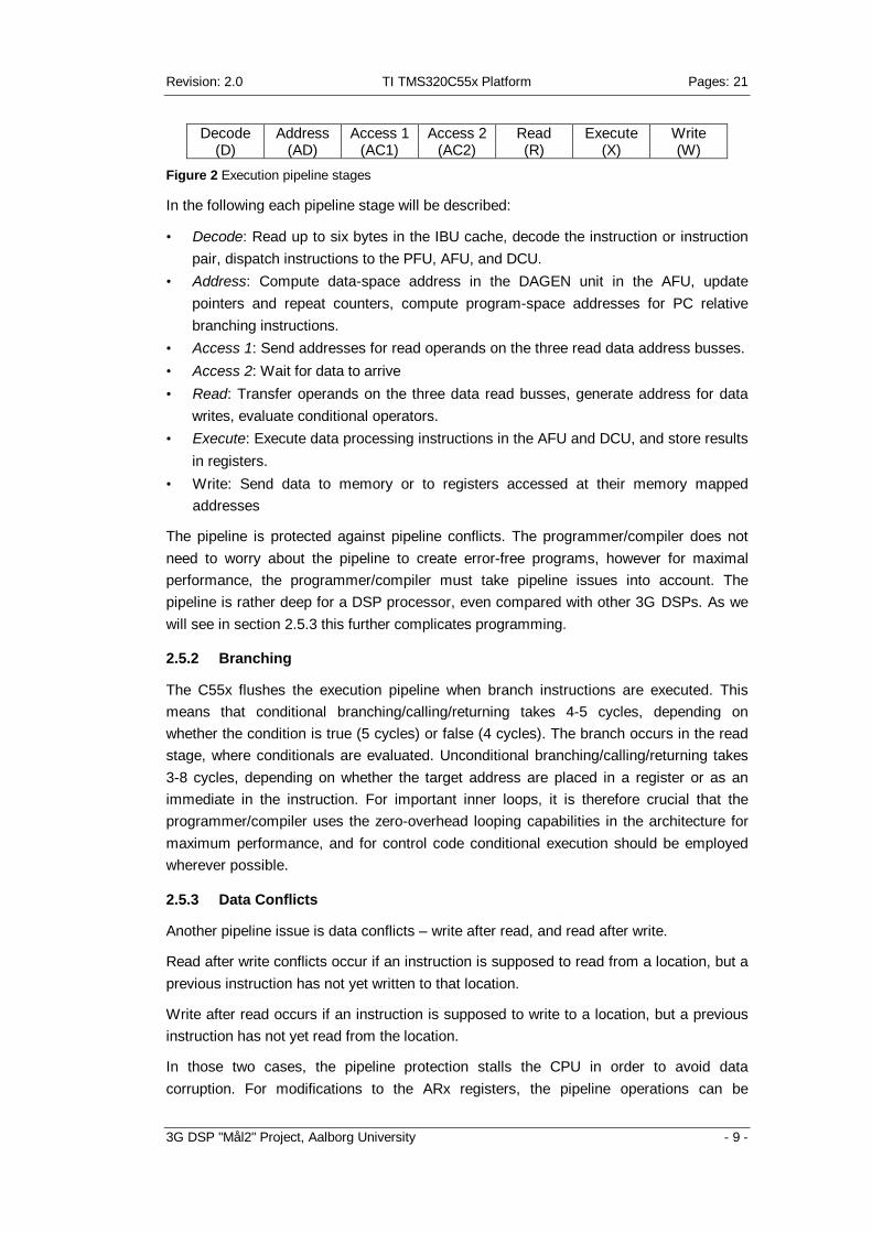
The C55x uses pipelining to improve the instruction throughput. In this section thepipeline stages will be presented.
2.5.1 Pipeline Stages
The pipeline is divided in two parts: The first part fetches instructions to the instructioncache in the IBU. The second part is called the execution pipeline. The execution pipelineis 7 stages deep, and is shown on Figure 2.
Revision: 2.0 TI TMS320C55x Platform Pages: 21
3G DSP "Mål2" Project, Aalborg University - 9 -
Decode(D)
Address(AD)
Access 1(AC1)
Access 2(AC2)
Read(R)
Execute(X)
Write(W)
Figure 2 Execution pipeline stages
In the following each pipeline stage will be described:
• Decode: Read up to six bytes in the IBU cache, decode the instruction or instructionpair, dispatch instructions to the PFU, AFU, and DCU.
• Address: Compute data-space address in the DAGEN unit in the AFU, updatepointers and repeat counters, compute program-space addresses for PC relativebranching instructions.
• Access 1: Send addresses for read operands on the three read data address busses.• Access 2: Wait for data to arrive• Read: Transfer operands on the three data read busses, generate address for data
writes, evaluate conditional operators.• Execute: Execute data processing instructions in the AFU and DCU, and store results
in registers.• Write: Send data to memory or to registers accessed at their memory mapped
addresses
The pipeline is protected against pipeline conflicts. The programmer/compiler does notneed to worry about the pipeline to create error-free programs, however for maximalperformance, the programmer/compiler must take pipeline issues into account. Thepipeline is rather deep for a DSP processor, even compared with other 3G DSPs. As wewill see in section 2.5.3 this further complicates programming.
2.5.2 Branching
The C55x flushes the execution pipeline when branch instructions are executed. Thismeans that conditional branching/calling/returning takes 4-5 cycles, depending onwhether the condition is true (5 cycles) or false (4 cycles). The branch occurs in the readstage, where conditionals are evaluated. Unconditional branching/calling/returning takes3-8 cycles, depending on whether the target address are placed in a register or as animmediate in the instruction. For important inner loops, it is therefore crucial that theprogrammer/compiler uses the zero-overhead looping capabilities in the architecture formaximum performance, and for control code conditional execution should be employedwherever possible.
2.5.3 Data Conflicts
Another pipeline issue is data conflicts – write after read, and read after write.
Read after write conflicts occur if an instruction is supposed to read from a location, but aprevious instruction has not yet written to that location.
Write after read occurs if an instruction is supposed to write to a location, but a previousinstruction has not yet read from the location.
In those two cases, the pipeline protection stalls the CPU in order to avoid datacorruption. For modifications to the ARx registers, the pipeline operations can be
Revision: 2.0 TI TMS320C55x Platform Pages: 21
3G DSP "Mål2" Project, Aalborg University - 10 -
overridden manually. For an instruction like : ARx = ARy the data transfer from ARy to
ARx occur in the execution stage. However, by specifying the instruction with the mar()qualifier like this: mar(ARx = ARy) the data transfer occurs in the Address phase. Thiscan be used to avoid stalls when loading variables as in the following example:
AR1 = #y ; AR1 updated in the execution stage; 3 CPU stalls are inserted
AC0 = *AR1 ; AR1 read in the address stage
mar(AR1 = #y) ; AR1 updated in the address stageAC0 = *AR1 ; AR1 read in the address stage… ; No CPU stalls was inserted
Therefore modifications to the ARx registers should be specified as an mar() instructionto avoid pipeline stalls in certain cases. For other registers, the programmer/compilermust schedule instructions properly to avoid pipeline stalls, which further complicatesprogramming.
2.6 Instruction set
The instruction set is large and complex. All instructions execute in one cycle, except forthe branch/call/return instructions. There are more than 400 entries in the instruction setsummary, however many of the instructions are very similar, see the following example:
Syntax for some addition instructions (there exist 12 additional addition instructions):
dst = dst + src ; dst and src are ARx, ACx or Tx registersdst = dst + k4 ; k4 is an unsigned 4 bit constantdst = src + K16 ; K16 is a signed 16 bit constantdst = src + Smem ; Smem is a 16-bit operand from memory
As indicated by the above example, an instruction exist depending on whether theoperands come from registers, the instruction word, or a memory location, i.e., the C55xarchitecture is CISC-like. When programming, the programmer does not need to beaware of which specific instruction he uses, because the assembler automatically selectsthe shortest one that does what the programmer specifies. An example:
T2 = T2 + #17
The above instruction will be translated into the "dst = src + K16" instructionbecause the constant cannot be represented by 4 bits. However, that instruction is 4bytes wide, compared to two bytes for the "dst = dst + k4" instruction. Although the
assembler automatically helps the programmer choosing the right instruction, theprogrammer/compiler should be aware of the differences in the instruction set for optimalcode generation.
When accessing memory operands, the following addressing modes is available:
• Absolute addressing mode• Direct addressing mode• Indirect addressing mode
Revision: 2.0 TI TMS320C55x Platform Pages: 21
3G DSP "Mål2" Project, Aalborg University - 11 -
2.6.1 Absolute Addressing Mode
In absolute addressing mode, the full data address is included as three additional bytes tothe instruction. Alternatively only the lower 16 address bits are added to the instructionword, and the data page is taken from the DPH register. Either way, when using absoluteaddressing the instruction cannot be executed in parallel with other instructions due to theextended instruction width (see section 2.8.2). Furthermore, when the full 23 bit addressis specified, some instructions take another cycle to execute.
2.6.2 Direct Addressing Mode
The direct addressing mode can be used to access data using a 128 word offset. Theoffset is relative to either the DP/DPH or SP/SPH registers, and the instructions has a 7bit offset which is added to either DP/DPH or SP/SPH. Which pair of registers that is useddepends on a bit in the ST1 status register. The DP/DPH mode is used when accessingoperands using direct addressing mode in general, and the SP/SPH mode is used toaccess variables pushed onto the stack. When the C compiler is used, the SP/SPH isalways used.
2.6.3 Indirect Addressing Mode
Indirect addressing mode is used to access data using the ARx registers as pointerregisters containing the address. Modification of the ARx register can occursimultaneously when indirect addressing mode is used. The possible uses are:
• No modification of ARx• Pre/post-increment/decrement by one• Post increment/decrement by content of register T0/AR0, possibly with reverse carry
propagation for bit-reversed addressing• Post increment/decrement by content of register T1• No modification of ARx, but data address is offset by content of T1/T0/AR0• Post increment by signed 16 bit constant• No modification of ARx, but data address is offset by signed 16 bit constant
Except for the bit-reversed mode, all indirect addressing mode can be used for eitherlinear or circular addressing mode, depending on the status register settings.
There are some limitations for some of the modes. If two individual memory operands areused in same cycle, such as in dualMAC and some single MAC instructions, the followingthings are prohibited:
• Pre-modification of the ARx registers• Bit-reversed addressing• 16-bit constant offset or post increment
For accessing full data read bandwidth it is necessary to use the CDP register as apointer, to control the transfers over the B data read bus. However, the modifications tothe CDP register when full memory bandwidth is necessary are limited to post-increment/decrement, and post-increment by the contents of T0/AR0.

Revision: 2.0 TI TMS320C55x Platform Pages: 21
3G DSP "Mål2" Project, Aalborg University - 12 -
Furthermore the addressing modes are divided into "DSP" mode and "control" mode.Which mode that is active is controlled with the AR Modifier Status (ARMS) status bit. In"control" mode, a short immediate offset mode is available, that helps in keeping codesize down. In "DSP" mode, bit reversed addressing and some more AR modifier optionsare available (register T1 can also be used as a post increment modifier).
As evident from above, there are many addressing modes available in the architecture.However for time-critical code, where the use of the processors resources must bemaximized cycle by cycle, there are constraints on which modes that should be used.However, the constraints should be easy to avoid, as long as the programmer/compilerare aware of the limitations.
2.6.4 Instruction Set Orthogonality
The instruction set cannot be said to be orthogonal. There are dedicated addressregisters and accumulator registers. E.g. multiplications and MAC instructions must placethe result in one of the accumulator registers.
Compared to traditional DSP architectures, there are more registers available of eachtype, and this makes the restrictions less significant. Compared to the Lucent DSP16000,which is another enhanced conventional DSP architecture with a dual MAC datapath, thisarchitecture contains twice as many accumulator registers as the C55x. However, theLucent architecture implements a RISC like instruction set, where all variables must beloaded into registers before they are manipulated, whereas the C55x can operate onmemory operands directly, thus four accumulator might be enough to avoid heavyregister spilling for most purposes.
2.7 Hardware Modes
The C55x processor has many modes of operation. Many modes concern the arithmeticbehavior of the functional units, and one mode concern the indirect addressing modesavailable (the ARMS mode setting). These have been explained throughout thedocument.
As stated previously, the C55x is assembly code compatible with it's predecessor, theC54x. However, it requires that the C54x operates in a special C54x compatible mode,which is controlled with a mode bit in status register 1, C54CM.
Another mode setting, is whether direct addressing is done relative to the data pageregister (DP), or the stack pointer register (SP). When the compiler is used, the processormust be in SP direct addressing mode. This mode is also referred to as compilercompatible mode. This mode is controlled with the CPL bit in status register 1.
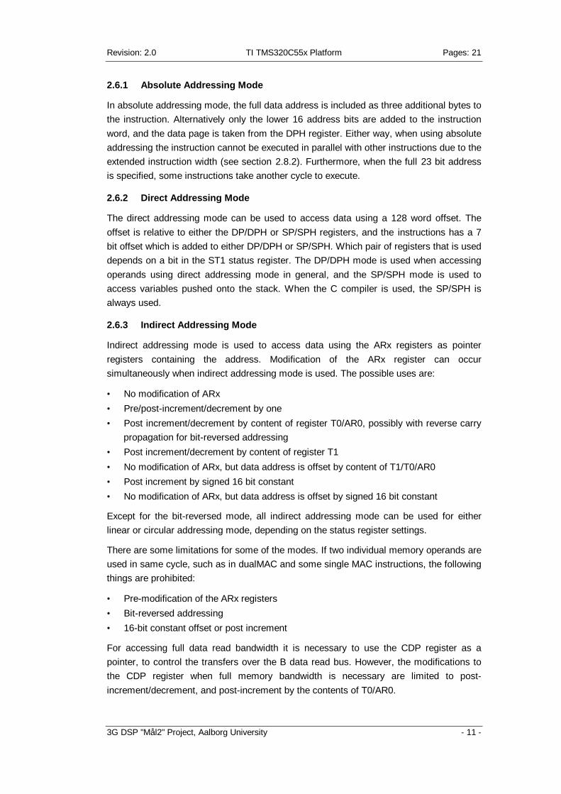
The instruction set contains an idle instruction that puts the hardware into idle mode.The C55x is targeted towards low power applications, and the idle mode is configurableto a high degree. When an idle instruction is executed, individual parts of the processor isput to sleep according to the idle configuration register (ICR). This is done by copying theICR to the idle status register, which controls which parts of the processor that is idle.This is shown on Figure 3.
Revision: 2.0 TI TMS320C55x Platform Pages: 21
3G DSP "Mål2" Project, Aalborg University - 13 -
Figure 3 Overview over the idle mode process, and which processor domains that can beindividually controlled.
There are some restrictions on which combinations of domains that can be put to sleep.E.g., the CLKGEN domain, which is the DSP clock generator, cannot be put to sleep ifDMA or the CPU is not put to sleep.
Interrupts are able to wake parts of the processor up in order for it to continue operation,if the CPU and/or the CLKGEN domains are put to sleep. If the CPU domain is not put tosleep, a new idle configuration can be activated by issuing another idle instruction.
2.8 Programming Model
In this section, the programming model in terms of the assembly language format and therestrictions on parallelism is presented. In the previous sections, the issues concerningpipeline stalls and addressing mode restrictions on parallelism have been covered, andthey will not be presented here, however, they are still important issues for aprogrammer/compiler.
2.8.1 Assembly Language Format
The C55x assembler supports two different assembly language formats:
• Mnemonic instruction set format, example: MACM *AR2+, *AR3+, AC3
• Algebraic instruction set format, example: AC3 = AC3 + ((*AR2+) * (*AR3+))
The algebraic instruction format has the advantage of being easy readable, but thedisadvantage that instruction disambiguaty can occur. Instruction disambiguaty meansthat algebraic instruction expression format is identical for two or more instructions. Insuch cases, the assembler selects the shortest instruction.
2.8.2 Efficient Code: Use All Resources All the Time
As previously described, the C55x is a multi issue architecture with an instruction set thatincludes compound instructions that specify many operations. In this section the possiblelevels of parallelism as provided by the processor will be described.

Revision: 2.0 TI TMS320C55x Platform Pages: 21
3G DSP "Mål2" Project, Aalborg University - 14 -
As previously described, parallelism can be obtained in two ways:
1. Built-in parallelism within a single instruction: several operations are encoded in oneinstruction. These instructions are directly shown in the instruction set summary, andinclude e.g., dual multiply and multiply-and-accumulate instructions.
2. User-defined parallelism between two instructions: This is obtained by the assemblylanguage programmer or the compiler. Parallelism between two instructions arespecified with two parallel bars ( || ) between the instructions.
Both forms of parallelism can be combined. The basic rules for using the user-definedparallelism are:
• Instruction length: Two instructions can be put in parallel if the added length of theinstructions does not exceed 6 bytes.
• Parallel enable bit: One of the instructions must have a parallel enable bit. Theinstruction set summary shows this for each instruction. A large subset of theinstruction set does have this bit.
• Hardware resources: Two instructions can be put in parallel if they do not sharehardware resources (functional units, buses, and output registers).
3 CompilerTexas Instruments supply an ANSI C compatible compiler, and a future release whichsupports C++ are in development, according to the readme.txt file with the codegeneration tools version 1.70. In fact, the 1.70 version of the tools support a preliminaryrelease of the C++ support. The description of the compiler will be based on [TI, 2000c],however that document description is based on version 1.20 of the code generation tools,and the benchmarking will be performed with the 1.70 version of the tools. Therefore,where changes have occurred, the readme.txt file from the 1.70 tools take precedenceover the [TI, 2000c] document.
3.1 Options/Which Optimizations?
3.1.1 Optimization levels
The following table shows which optimizations that is performed on the intermediaterepresentation by an optimization pass in the compiler. In addition, the code generator,which generates the assembly code from the intermediate representation, performstarget-specific optimizations independently of the optimization in the table, but theseoptimizations are not specified further in the compiler documentation.
Optimization level Optimizations performed-o0 • Performs control-flow-graph simplification (branch optimization,
conditional execution)• Allocates variables to registers• Performs loop rotation (evaluate loop conditionals at the
bottom)

Revision: 2.0 TI TMS320C55x Platform Pages: 21
3G DSP "Mål2" Project, Aalborg University - 15 -
• Eliminates unused code• Simplifies expressions and statements• Expands calls to functions declared inline
-o1 Performs all –o0 optimizations, plus:• Performs local copy/constant propagation• Removes unused assignments• Eliminates local common expressions
-o2 Performs all –o1 optimizations, plus:• Performs loop optimizations• Eliminates global common subexpressions• Eliminates global unused assignments• Performs loop unrolling
-o3 Performs all –o2 optimizations, plus:• Removes all functions that are never called• Simplifies functions with return values that are never used• Inlines calls to small functions• Reorders function declarations so that the attributes of called
functions are known when the caller is optimized• Identifies file-level variable characteristics
Table 6 Optimizations performed at different levels
As the table shows, the C55x compiler includes all the standard target independentoptimizations, as well as some more advanced file-level optimizations when applyinglevel –o3.
From version 1.70, the compiler should be able to generate dual MAC instructions. Inorder to do this, the switch "-mb" must be used, which is a promise to the compiler that alldata are on-chip. This is necessary because the b-bus, which is shared between the twoMAC units, are only connected to on-chip memory.
The C55x compiler will compile the source files one by one, even if several files arespecified on the same command line, which is common practice for compilation.However, this approach is not optimal if you have a software design with a few interfacefunctions to a module, and these interface functions call a number of functions which arenot called by others. In the cases of such a software design, it would be beneficial for thecompiler to get this information in order to optimize the "sub-functions" based on whichparameters they are called with. This could be obtained by writing all of the modulesource code in one file, and declaring the "sub-functions" static, informing the compilerthat these functions are only called by the interface functions in this file. This approachwould unleash the full power of file-level optimizations. However, for many reasons, it isnot optimal to keep the source code for an entire module in one source file. Therefore, TIhas an interlisting utility, which is supplied with their compilers, that combines severalsource files into one source file, before compilation is performed. This can be invokedwith the option –pm when optimization level –o3 is used. Doing this, the compilerassumes that all functions are declared static, except when a pragma is used to indicate
Revision: 2.0 TI TMS320C55x Platform Pages: 21
3G DSP "Mål2" Project, Aalborg University - 16 -
which functions that are externally called, and this allows the compiler to get the most outof the file-level variable characteristics analysis.
The compiler performs alias analysis in order to determine whether two pointers point tothe same object, as aliasing can influence the optimizations. The optimizer behavesconservatively, and if there is a chance that two pointers point to the same object, thecompiler assumes that they do. There is one exception: the optimizer assumes that anyvariable whose address is passed as an argument to a function is not subsequentlymodified by an alias set up in the function. This should rarely occur, as aliasing shouldgenerally be avoided in a good programming style. If it occurs, the flag –ma must be usedin order for the compiler to produce correct code.
The compiler default optimizes to decrease execution speed. The –ms option can beused to inform the compiler to give code size priority over execution speed, when aselection must be made.
The automatic inlining of functions which are used with –o3, can be controlled with the –oiXX, where XX specifies the size of the functions to inline. Default, only small functionsare inlined.
Besides the mentioned optimization switches, which affect the generated code, there area number of switches to generate assembly files, interlisting files, optimization informationfiles, control interpretation of file extensions, control whether compiling, assembling, andlinking should be done in one or several steps, enable symbolic debugging, suppressbanners, etc.
3.2 Language Implementation
The ANSI C standard leaves some aspects of the language implementation specific, i.e.,they can very from compiler to compiler. The most important of these are therepresentation of the C data types, and the implementation of right shift on signedintegers.
3.2.1 Data Types
The data type implementation is shown in Table 7.
Data type RepresentationChar, short, int 16 bit integerLong 32 bit integerLong long 40 bit integerFloat, double, long double IEEE 32-bit floating pointPointer (small memory model) 16 bitPointer (Large memory model) 23 bit
Table 7 Data types and their implementation for the C55x C compiler
The native data type (int) is chosen to be 16 bit, which is natural as the processors maindata type is 16 bits. However, this leaves only one larger data type, (long), which ischosen to be 32 bit. This is to a degree unfortunate, as the accumulators in fact are 40

Revision: 2.0 TI TMS320C55x Platform Pages: 21
3G DSP "Mål2" Project, Aalborg University - 17 -
bits, and it would be desirable to have access to the full width of the accumulators from C.Although not stated directly in the documentation, it seems like a "long long" data typeexist in the compiler, which has a 40 bit representation, and this can be used to haveaccess to the full width of the accumulator registers.
3.2.2 Right Shift Operator
The right shift operator implements an arithmetic right shift, i.e., the sign is preservedwhen used on signed integers.
3.3 Language Extensions / Pragmas / Intrinsics
The C55x compiler supports a number of pragmas, some intrinsics, and inline assemblylanguage statements. There are no language extensions to support fractional arithmetic,saturation, rounding, and circular buffers, which are important to DSP applications.
3.3.1 Pragmas
There are 12 pragmas. Seven of these are used to specify properties of functions, suchas the pragma to indicate that functions are externally called when applying program leveloptimizations. The other pragmas can be used to define which sections code and datashould be linked into, and to interface C55x code calls to functions to C54x code.
The compiler also support the _nassert() intrinsic. However, the _nassert() intrinsic doesnot generate any code, but is used to pass information to the compiler, and therefore weclassify it as a pragma rather than as an intrinsic. _nassert() can be used to passinformation about properties of variables in C, such as minimum and maximum loopcount, or whether the loop count is always a multiple of X, and whether arrays are alignedon a 32-bit boundary. This information can be useful for the compiler, in order to generatenear-optimal loop code. However, if interlisting of multiple source files is used (-pm), thecompiler should be able to deduce properties of many of the variables automatically.
3.3.2 Intrinsics
The C55x compiler offers more than 25 intrinsics, which are written in C as function calls,but they are mapped onto specific assembly instructions, or sequences of assemblyinstructions. These are used to provide easy access to DSP functionality which is hard toexpress in C, such as saturated addition, fractional multiplication with saturation and/orrounding, etc.
In the 1.70 version, there is also some new 40-bit intrinsics to perform 40-bit saturation,negation, addition, and subtraction.
3.3.3 Inline Assembly
Inline assembly language statements can be inserted from the C code by using theasm("") statement. However, the compiler does not analyze what is inserted in this way,and therefore this can lead to undesirable results. This is especially true if the optimizer isused, as this can result in rearrangement of the code and the assembly statement can

Revision: 2.0 TI TMS320C55x Platform Pages: 21
3G DSP "Mål2" Project, Aalborg University - 18 -
have other effects than desired. TI does not recommend the use of inline assemblystatements when the optimizer is invoked.
3.4 Run Time Environment
This section describes how the compiler views upon memory, and which conventions ithas for the use of registers and parameter passing.
3.4.1 Memory Model
The compiler treats memory as a single linear block, which is partitioned into segments ofcode and data. Two modes of operation are used:
1. Small memory model2. Large memory model
The small memory model results in a slightly smaller code size and execution time, as ituses 16-bit pointers and thus assumes that all data fit within one 64 kbyte block. This isthe default mode.
In the large memory model there are no restrictions on the placement of data. Pointersare represented by 23 bits, and occupies two 16-bit words when stored in memory.
The compiler produces relocatable blocks of code and data, which are called sections.The linker can be used to control how these sections are placed in memory.
3.4.2 Register Conventions
The register conventions of the C55x compiler is shown in Table 8.
Registers Usage by the Compiler Argument Passing?Preserved by calling function
AC0-AC2 16-, 32-, 40-bit data, or 24-bit code pointers 32-bit dataAC3 --||-- NoneAR0(H)-AR4(H) 16-, or 23-bit pointers or 16-bit data Pointers or 16-bit dataT0, T1 16-bit data 16-bit dataControl (Except ST0 – ST3) None
Preserved by called functionAR5(H)-AR7(H) 16-, or 23-bit pointers or 16-bit data NoneT2, T3 16-bit data None
Table 8 The compiler's usage of registers, how register data are preserved, and which registers areused for argument passing. The status registers are treated in a special way, and are not present inthe table.
The control registers are treated in a special way. The compiler assumes that some of thestatus bits has a certain value on function entry and exit. For example, it assumes thatrounding, saturation, 40 bit accumulation are disabled on function entry and exit.However, the documentation states that the compiler is able to modify these status bits,i.e., it is able to exploit this functionality in the hardware, although it might only be throughintrinsics that the compiler is able to do so.

Revision: 2.0 TI TMS320C55x Platform Pages: 21
3G DSP "Mål2" Project, Aalborg University - 19 -
3.4.3 Calling Conventions
The basic structure of a function call are the following:
1. The calling function saves the registers it must preserve if they contain data that isused after the function call
2. The calling function puts parameters in registers or on stack. As evident from Table 8,up to 10 parameters can be passed in registers.
3. The call takes place. The hardware automatically pushes the return address on stack.4. The called function allocates space on the stack for local data, temporary storage,
and arguments to functions this function might call.5. The called function executes the code. If any save-on-entry registers are modified, it
must preserve the value by copying the register to another register or push it ontostack, and copying the value back before function return.
6. The return value from the called function are placed in AC0, T0, AR0, depending onwhether it is a 32-bit value, 16-bit value or a pointer.
7. The stack pointer is restored to its original value.8. The return happens – PC is popped of the stack by the hardware.9. The return value is read by the calling function.
If a struct or a union is passed as an argument or a return value, the above function callstructure are changed slightly.
3.5 Optimization Strategy
In the programmer's guide the following approach is proposed:
1. Write C code: Write ANSI C code without assuming knowledge of the C55x DSP.2. Optimize C code: Use specific C-types (const), modify the C code to better suit the
C55x architecture, use intrinsics3. Write assembly code: Rewrite the performance critical portions of the software as C-
callable assembly routines.4. Optimize assembly code: Parallelize assembly code, reorganize code to avoid
pipeline stalls
Step 4 can appear a bit superfluous – why not write the assembly code in an optimalmanner the first time? But on the other hand it does make sense to write the assemblycode initially with all the focus on getting the loops optimal, and afterwards the rest of thecode can be optimized.
In step 2, they don't mention pragmas – they should be applied as well at this point. Themodification of the C code to better suit the C55x architecture involves:
• Doing a proper memory layout to avoid stalls due to parallel memory accesses• Place the most frequently path first in a switch statement or nested if-constructs to
speed up execution of control-oriented code• Avoid function calls in loop bodies• Keep loop bodies small to allow for usage of zero-overhead looping
Revision: 2.0 TI TMS320C55x Platform Pages: 21
3G DSP "Mål2" Project, Aalborg University - 20 -
The documentation are valid for single MAC generation, but as previously described thelatest compiler version should be able to generate dual-MAC instructions. This probablyrequires a special arrangement of the C code in order for the compiler to exploit dual-MAC instructions, due to the nature of the C55x architecture where the two MAC unitsmust share one operand. Hopefully our investigations will reveal whether this isnecessary.
4 Simulator / Debugger / EmulatorThere is a cycle-accurate simulator, as well as a debugger integrated in TI's integrateddevelopment environment, Code Composer Studio, which looks similar to Visual C++from Microsoft. An emulator is also available through Code Composer Studio.
The simulator can be accessed through a command window, where commands can beissued to the simulator in a proprietary language. It also has the ability to do batchprocessing, i.e., load a text file with commands and run those. This enables the possibilityfor a large degree of automation in the profiling and simulation process.
The simulator that comes with CCS 1.20 does not include stalls due to parallel memoryaccesses to the same block, however the simulator that comes with CCS 2.0, which areto be released in 1H2001, should include modelling of memory access stalls.
5 Strategy for Case StudiesDue to CCS instabilities, the best approach is to do the compilation with makefiles andthe GNU make utility. This way, it is also easier to store the experiments in a reproduciblemanner. The same reason is valid for using the command window and batch files to runthe simulations and profiling.
The following optimization levels seems reasonable to investigate for this platform:
0. ISO C version
1. Optimized ISO C version. Rearrangement of loops to use dual MAC capabilities andrearrangement of switches to place the most frequent entry first are obviousoptimizations.
2. Use pragmas to distribute data optimally in memory.
3. Use _nassert(), pragmas, intrinsics.
4. Assembly code implementation. This should be done for a few, smaller benchmarks.
As a general rule, the following options affecting the assembly code output will be appliedfor time-constrained code:
-o3 –mb –pm
This enables maximum optimizations, dual-MAC exploitation, and interlisting of sourcefiles, i.e., program level optimizations. On some benchmarks it may be interesting toinvestigate the difference between using –pm and not using –pm, as this is a featurewhich is rarely seen in a compiler.
Revision: 2.0 TI TMS320C55x Platform Pages: 21
3G DSP "Mål2" Project, Aalborg University - 21 -
For size-constrained code, the following option is added: -ms.
It can be debated whether we should distribute data optimally in memory on the ISO Cand optimized ISO C versions, because the compiler does not try to distribute theseoptimally in memory, it places all data in the same section. For the small benchmarks, itcan be done both ways.
All fixed point benchmarks should be run on this benchmark. It doesn't make much senseto run floating point code on this platform, as floating point operations are emulated vialibrary calls.
6 Literature[Lapsley, 1996] DSP Processor Fundamentals: Architectures and Features, Phil
Lapsley, Jeff Bier, Amit Shoham, Edward A. Lee, IEEE Press, ISBN:0780334051
[TI, 2000a] C55x Basic Workshop, Parkens Conference Center, October 2-4 2000,presented by Hervé Marechal, Field Application Engineer,Semiconductor Technical Marketing, Texas Instruments.
[TI, 2000b] TMS320C55x DSP CPU Reference Guide, Preliminary Draft,document number SPRU371C, May 2000.
[TI, 2000c] TMS320C55x Optimizing C Compiler User's Guide, document numberspru281a, April 2000.
[TI, 2000d] TMS320C55x DSP Functional Overview, document number spru312,June 2000.
The TI documents are available from http://www.ti.com/. (search for the documentnumber).