ti omap4430 pop smt design guideline (rev. c) · pdf fileti omap4xxx pop smt design guideline...
TRANSCRIPT
1
TI OMAP4xxx POP SMT Design Guideline
We Support
Michael Chen (TITL PKG)Kenji Masumoto (HIJI PKG)Shawn Wu (TITL PKG)Kurt Wachtler (WTBU PKG)
2
Index:
Package IntroductionOMAP4 SMT Process sharing
Appendix
Stencil/PCB design guideMemory chip flux/solder dipping in 1-step mountingThe example of Pick & Place machine condition settingReflow profile recommendationSMT experiment examples
Through molded via solder rework methodsX-ray examplesScreen print material and tool examplesPackage warpage affect examples
3
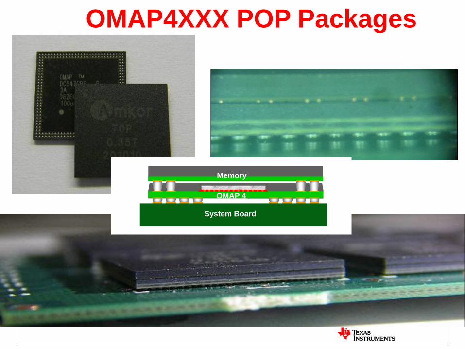
OMAP4XXX POP Packages
Memory
OMAP 4
System Board
4
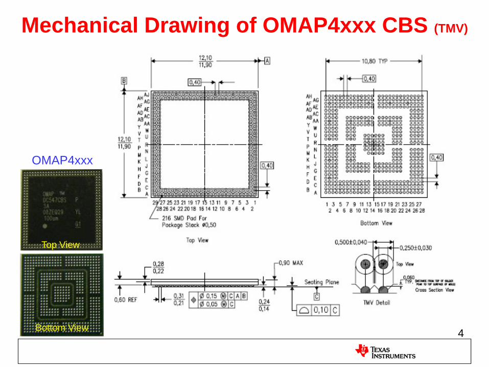
OMAP4xxx
Mechanical Drawing of OMAP4xxx CBS (TMV)
Top View
Bottom View
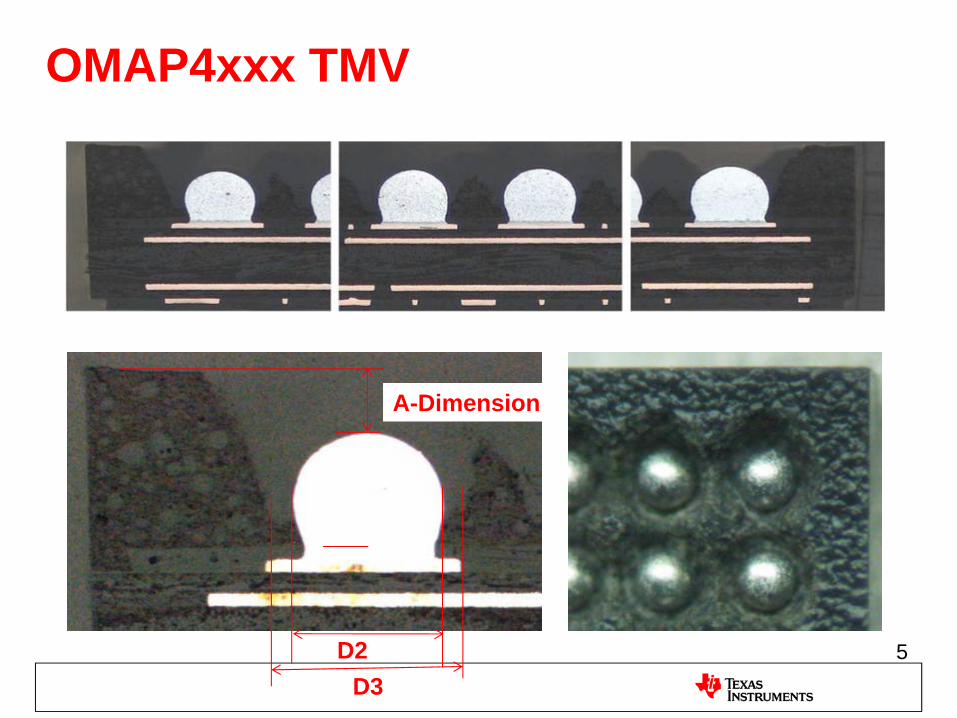
5
OMAP4xxx TMV
D2
A-Dimension
D3

6
Memory Chip
Mechanical Drawing of Memory Chip
Bottom View
7
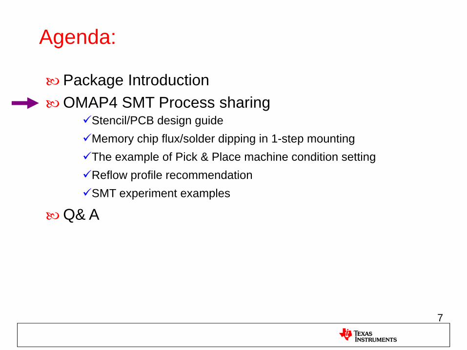
Agenda:
Package IntroductionOMAP4 SMT Process sharing
Q& A
Stencil/PCB design guideMemory chip flux/solder dipping in 1-step mountingThe example of Pick & Place machine condition settingReflow profile recommendationSMT experiment examples
8
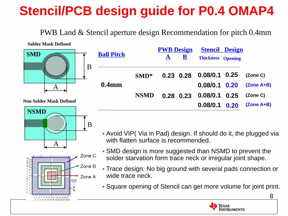
PWB Land & Stencil aperture design Recommendation for pitch 0.4mm
SMD
A
B
Solder Mask Defined
NSMD
A
B
Non Solder Mask Defined
Stencil/PCB design guide for P0.4 OMAP4
A B Thickness Opening
Stencil DesignBall Pitch
PWB Design
• Avoid VIP( Via in Pad) design. If should do it, the plugged via with flatten surface is recommended.
• SMD design is more suggested than NSMD to prevent the solder starvation form trace neck or irregular joint shape.
• Trace design: No big ground with several pads connection or wide trace neck.
• Square opening of Stencil can get more volume for joint print.
0.4mmSMD* 0.23 0.28 0.08/0.1 0.25
0.20(Zone C)
(Zone A+B)
NSMD 0.28 0.23 0.250.20
(Zone C)
(Zone A+B)
0.08/0.10.08/0.10.08/0.1
9
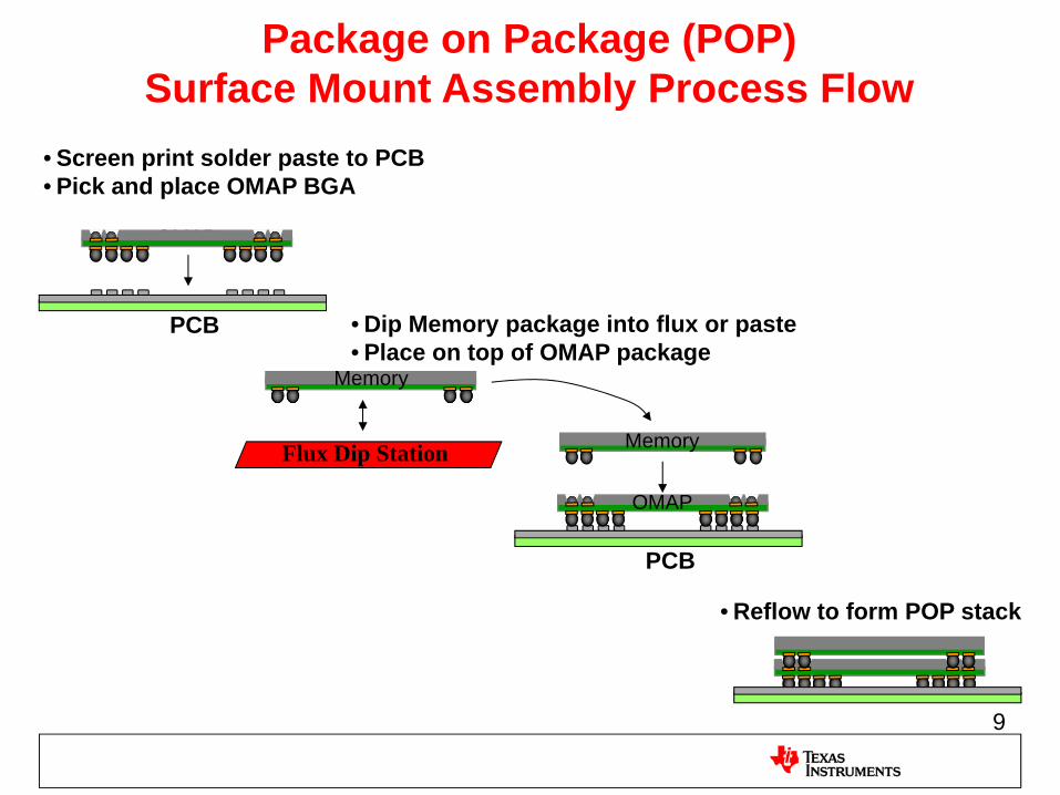
Package on Package (POP)Surface Mount Assembly Process Flow
• Screen print solder paste to PCB• Pick and place OMAP BGA
PCB
• Reflow to form POP stack
PCB
• Dip Memory package into flux or paste• Place on top of OMAP package
Flux Dip Station
Memory
OMAP
OMAP
Memory
10
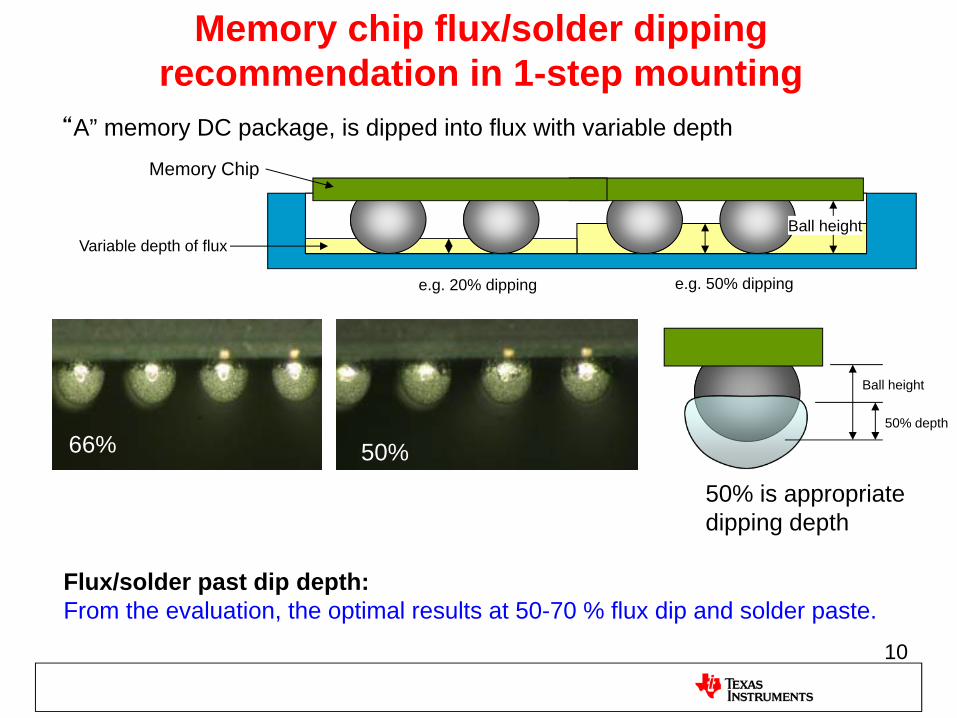
Flux/solder past dip depth:From the evaluation, the optimal results at 50-70 % flux dip and solder paste.
Variable depth of fluxBall height
e.g. 20% dipping e.g. 50% dipping
“A” memory DC package, is dipped into flux with variable depth
50%66%
50% is appropriate dipping depth
Ball height
50% depth
Memory chip flux/solder dipping recommendation in 1-step mounting
Memory Chip
11
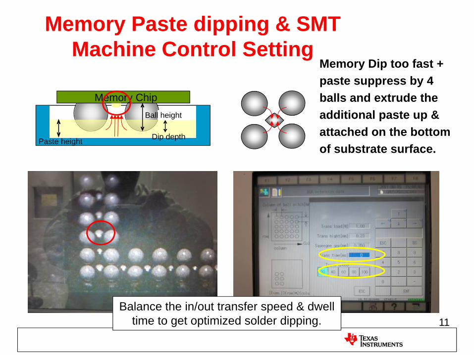
Memory Paste dipping & SMTMachine Control Setting
Memory ChipBall height
Dip depthPaste height
Balance the in/out transfer speed & dwell time to get optimized solder dipping.
Memory Dip too fast + paste suppress by 4 balls and extrude the additional paste up & attached on the bottom of substrate surface.
12
Flux/Solder Paste Depth Measurement
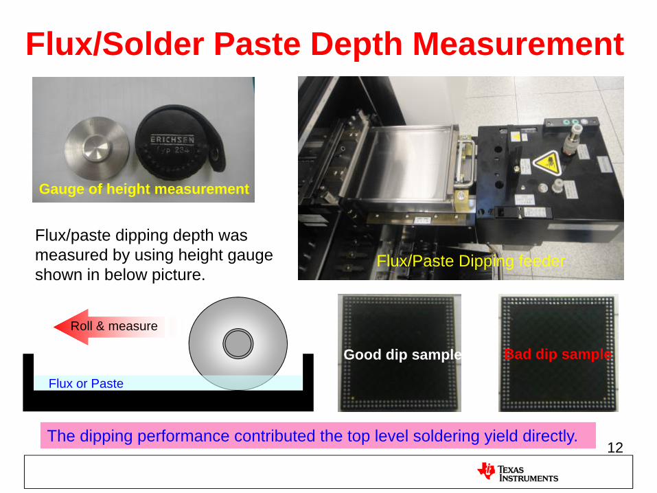
Flux/paste dipping depth was measured by using height gauge shown in below picture.
Gauge of height measurement
Flux/Paste Dipping feeder
Good dip sample Bad dip sample
Flux or Paste
Roll & measure
The dipping performance contributed the top level soldering yield directly.

13
Measurement of flux depth (Example)

14
Panasonic NPM
Next Production Modular
Nozzle type: 1004
Placement Parameters: Condition of PnP M/C setting (example)
SMT M/C Brand: PanasonicType: NPMDevice Placement: OMAP4 + Memory ChipPlacement method: By 1-stepFiducial marks recognition for placement: By Board fiducialPick up Nozzle type: 1004Nozzle size: ~8mm (with robber tip)Memory Vision sequence: Pickup + Camera vision + Memory Dipping + PlacementDwell time of memory dipping: 400ms ~1 secPlacement Force (N) or placement depth (um):
For OMAP4: package height+1~2.5N (push down)For Memory Chip: package height+1~2.5N (push down)
15
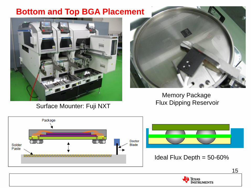
Memory PackageFlux Dipping ReservoirSurface Mounter: Fuji NXT
Ideal Flux Depth = 50-60%
Bottom and Top BGA Placement

16
Evaluated solder paste: Shenmao PF-606-P (SAC305)Tamura TLF-204-19A
Evaluated Memory dip flux/paste: Senju M705-TVA03.9F (Paste)Senju Deltalux-901K3 (Flux)
<700 ppm O2 reflow atmosphere is recommended to provide the widest process window.The real profile must be fine-tuned for each product to meet the optimized soldering results
RT to 150°C 1~3°C/sPre –heat temp(150~200 °C) 60~120secTime above melting 220°C 50~80secPeak temp 240-250°C Cool down rate 2~6°C/sec (max.)
Reflow conditions:
Preheating Stage Reflow Cool Down
250
200
150
100
50
Tem
pera
ture
–D
egre
es C
Time
Profile Recommendation for OMAP4xxx (TMV)
17
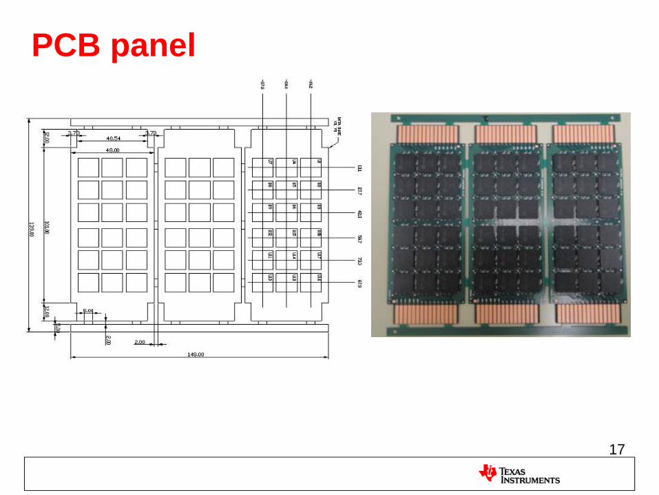
PCB panel
18
1
2
3
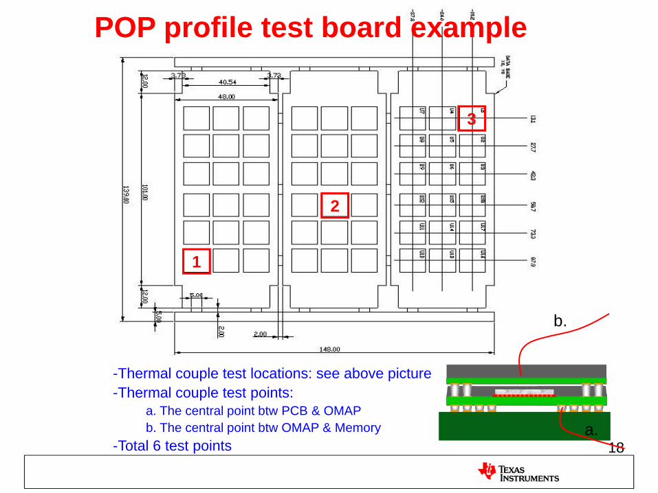
POP profile test board example
b.
a.
-Thermal couple test locations: see above picture-Thermal couple test points:
a. The central point btw PCB & OMAP b. The central point btw OMAP & Memory
-Total 6 test points

19
2-pass reflow: Pre-stack tray for FCPOP
To check temperature profile Pre-stack tray designed for TI OMAP3430
Pre-stack tray designed for TI OMAP3430
Bottom POP is supported bythis rib to depopulated ball area
20
Agenda:
Package IntroductionOMAP4 SMT Process sharing
Q& A
Stencil/PCB design guideMemory chip flux/solder dipping in 1-step mountingThe example of Pick & Place machine condition settingReflow profile recommendationSMT experiment examples
21
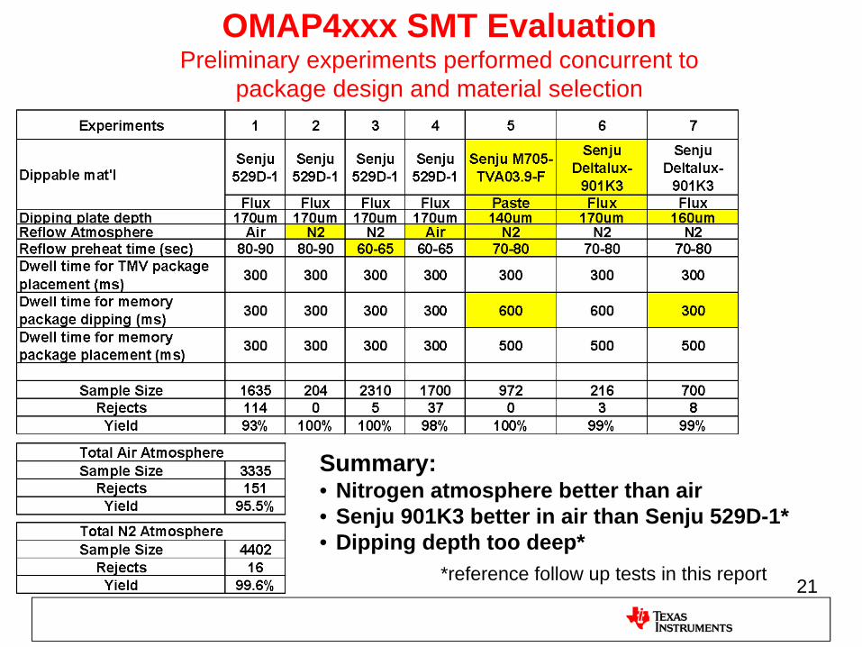
OMAP4xxx SMT Evaluation Preliminary experiments performed concurrent to
package design and material selection
Summary:• Nitrogen atmosphere better than air• Senju 901K3 better in air than Senju 529D-1* • Dipping depth too deep*
*reference follow up tests in this report

22
OMAP4xxx DOE Experiments
23
OMAP4xxx DC (TMV) SMT EvaluationDOE1
24
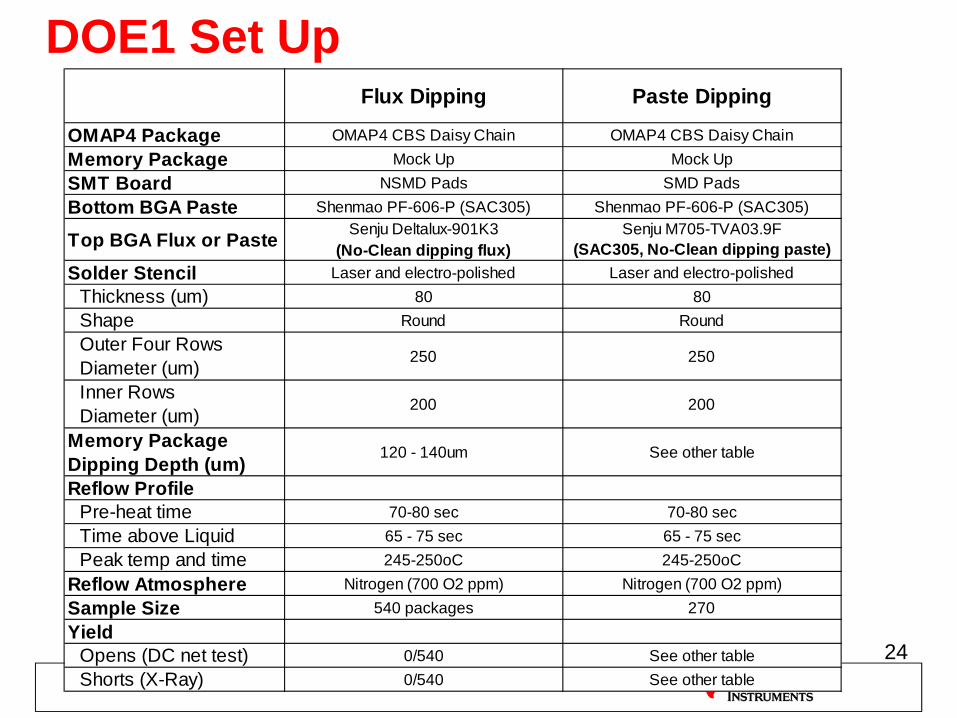
Flux Dipping Paste Dipping
OMAP4 Package OMAP4 CBS Daisy Chain OMAP4 CBS Daisy ChainMemory Package Mock Up Mock UpSMT Board NSMD Pads SMD PadsBottom BGA Paste Shenmao PF-606-P (SAC305) Shenmao PF-606-P (SAC305)
Top BGA Flux or Paste Senju Deltalux-901K3(No-Clean dipping flux)
Senju M705-TVA03.9F(SAC305, No-Clean dipping paste)
Solder Stencil Laser and electro-polished Laser and electro-polishedThickness (um) 80 80Shape Round RoundOuter Four RowsDiameter (um) 250 250
Inner RowsDiameter (um) 200 200
Memory PackageDipping Depth (um)
120 - 140um See other table
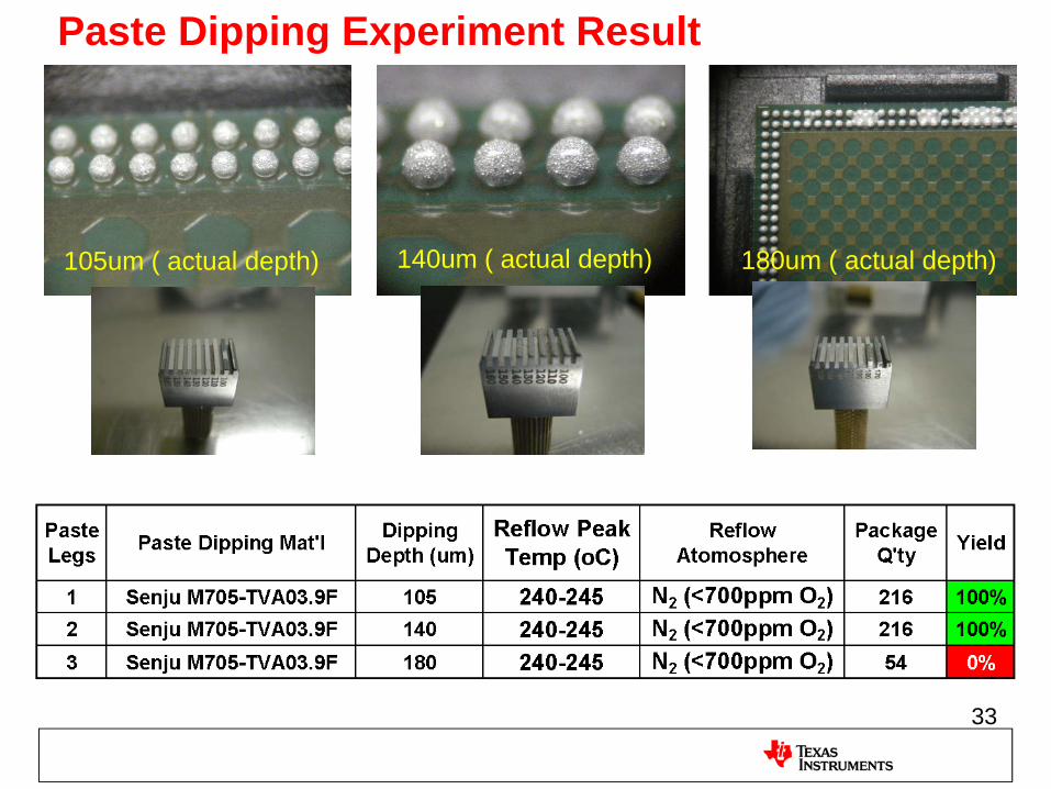
Reflow ProfilePre-heat time 70-80 sec 70-80 secTime above Liquid 65 - 75 sec 65 - 75 secPeak temp and time 245-250oC 245-250oC
Reflow Atmosphere Nitrogen (700 O2 ppm) Nitrogen (700 O2 ppm)Sample Size 540 packages 270Yield
Opens (DC net test) 0/540 See other tableShorts (X-Ray) 0/540 See other table
DOE1 Set Up
25
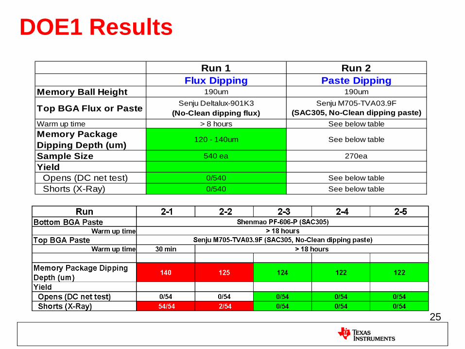
Run 1 Run 2Flux Dipping Paste Dipping
Memory Ball Height 190um 190um
Top BGA Flux or Paste Senju Deltalux-901K3 (No-Clean dipping flux)
Senju M705-TVA03.9F (SAC305, No-Clean dipping paste)
Warm up time > 8 hours See below tableMemory Package Dipping Depth (um)
120 - 140um See below table
Sample Size 540 ea 270eaYield
Opens (DC net test) 0/540 See below tableShorts (X-Ray) 0/540 See below table
DOE1 Results
26
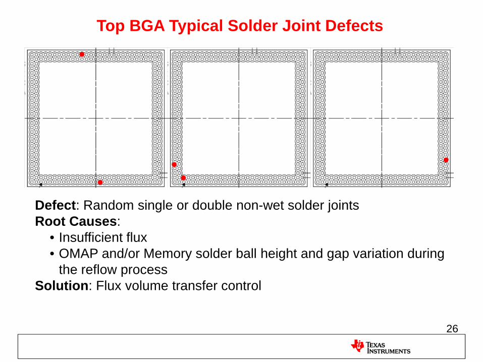
Top BGA Typical Solder Joint Defects
Defect: Random single or double non-wet solder jointsRoot Causes:
• Insufficient flux• OMAP and/or Memory solder ball height and gap variation during
the reflow processSolution: Flux volume transfer control

27
SMT Success
CustomerBoard
Reflow Process
Pick & Place
Package
Atmosphere:Air or N2
Paste & Flux
% Metal
Thixotropy/ Viscosity
PasteSlump
Solder Alloy
FluxActivation
Shelf/ Working Life
Solder Stencil
Material
Mfg Method
Surface finish
OpeningSize
Thickness
Openingshape
Print SpeedSqueegee
pressureSnap off
SeparationSpeed
Warpage
Pad Design
BGA Pitch
Warpage
Thermal Load
Bd & PanelDesignPkg Size
Accuracy
Dwell Time
Temperature Profile &
Uniformity
POP SMT Process Variables
Memory Dip Flux/Paste Volume Transfer
TMV Size
SolderAlloy
Solder Ball Size
SolderParticle Size
Pressure
Mold Cap Thickness
Memory Pkg
BOM
Solder Paste and Flux
Application
• TI Controlled• Standard POP Variables
• POP-TMV Variables

28
OMAP4xxx DC (TMV) SMT EvaluationDOE2
29
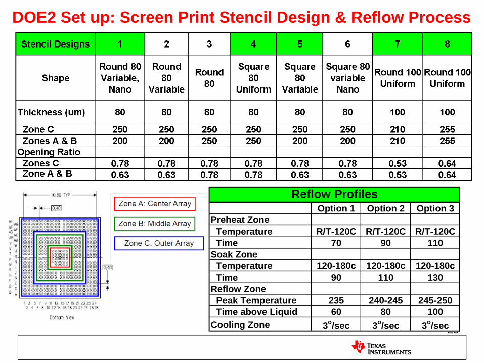
DOE2 Set up: Screen Print Stencil Design & Reflow Process
Option 1 Option 2 Option 3Preheat Zone
Temperature R/T-120C R/T-120C R/T-120CTime 70 90 110
Soak ZoneTemperature 120-180c 120-180c 120-180cTime 90 110 130
Reflow ZonePeak Temperature 235 240-245 245-250Time above Liquid 60 80 100
Cooling Zone 3o/sec 3o/sec 3o/sec
Reflow Profiles
30
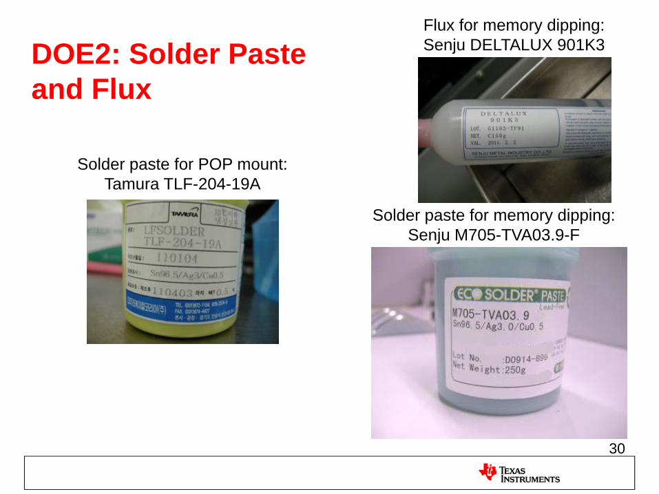
DOE2: Solder Pasteand Flux
Solder paste for memory dipping:Senju M705-TVA03.9-F
Flux for memory dipping:Senju DELTALUX 901K3
Solder paste for POP mount:Tamura TLF-204-19A
31
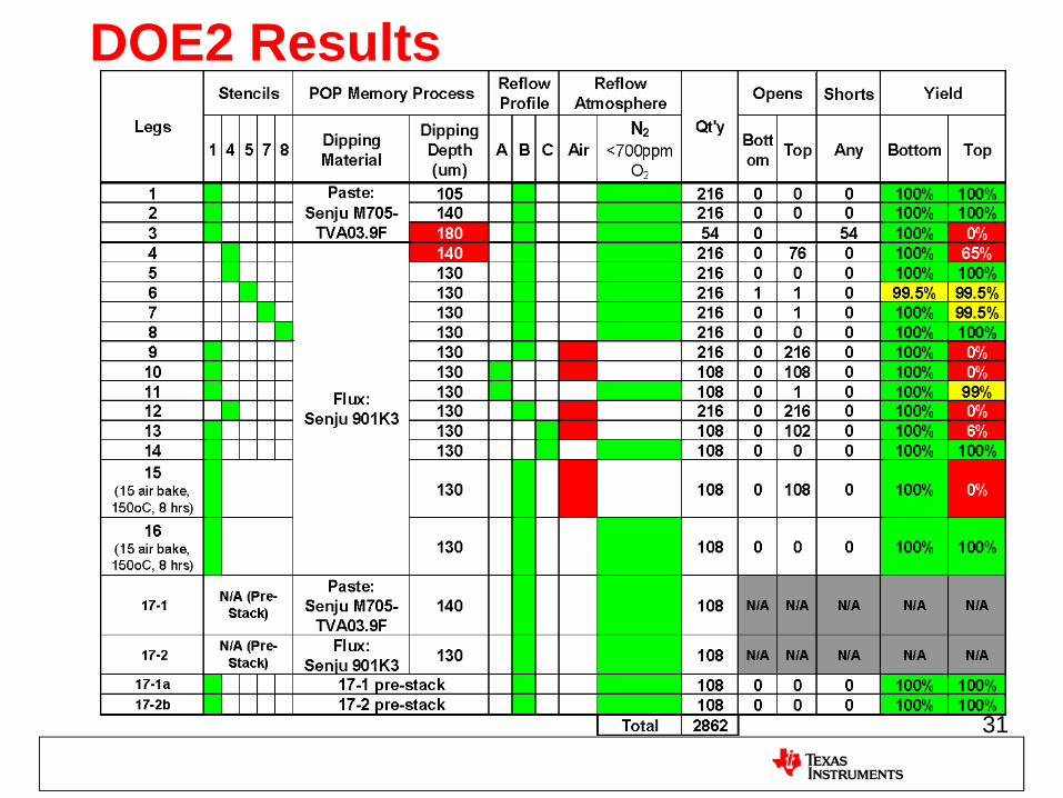
DOE2 Results
32
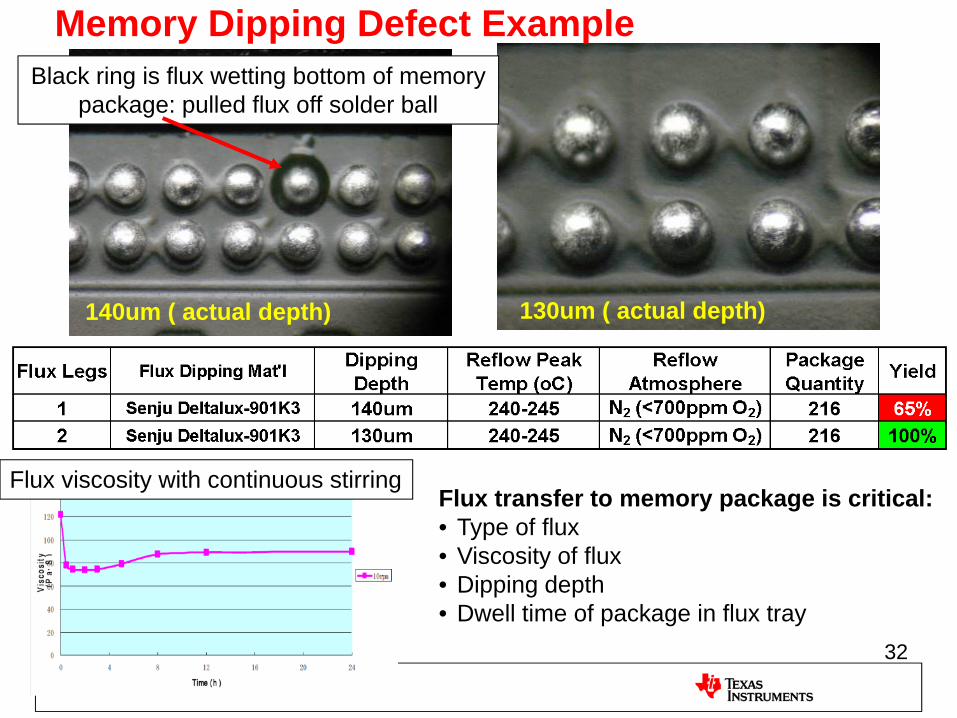
130um ( actual depth)140um ( actual depth)
Black ring is flux wetting bottom of memory package: pulled flux off solder ball
Flux transfer to memory package is critical:• Type of flux• Viscosity of flux • Dipping depth• Dwell time of package in flux tray
Flux viscosity with continuous stirring
Memory Dipping Defect Example
33
140um ( actual depth)105um ( actual depth) 180um ( actual depth)
Paste Dipping Experiment Result
34
DOE2 ResultSummary:• Bottom BGA yield robust vs. stencil design• Top BGA yield sensitive to flux dipping process
• Depth• Viscosity• Dwell time
• Top BGA dipping in paste successful: verification required• Nitrogen atmosphere (<700ppm O2) required in this test• Experiments will continue to define assembly capability in an Air reflow atmosphere

35
OMAP4xxx DC (TMV) SMT EvaluationDOE3
36
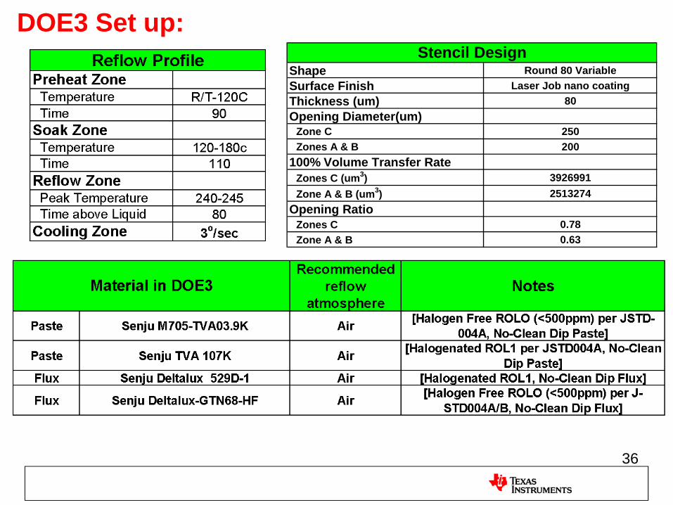
DOE3 Set up:Shape Round 80 VariableSurface Finish Laser Job nano coatingThickness (um) 80Opening Diameter(um)
Zone C 250Zones A & B 200
100% Volume Transfer RateZones C (um3) 3926991Zone A & B (um3) 2513274
Opening RatioZones C 0.78Zone A & B 0.63
Stencil Design

37
DOE3: Results
38
DOE3 ResultSummary:• Flux and Paste chemistry and rheology are critical factors for use in an air reflow atmosphere
• Time out of refrigeration and time worked in dipping tray affects coating uniformity
• Dipping time change from 600ms to 900ms improved yield• A paste that did not work in air worked in nitrogen reflow atmosphere
• Bottom BGA process continues to be robust• Pre-conditioned parts shifted and yielded zero bottom BGA connections: X-ray of top BGA looked normal but unable to test due to lack of connection through bottom BGA
39
AppendixA1: Through molded via solder rework methods
• Brush with flux repair method• Manual rework method
A2: X-ray examples A3: Screen print material and reflow equipment examplesA4: Package warpage affect examples
40
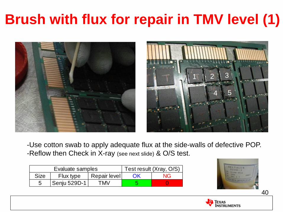
Brush with flux for repair in TMV level (1)
-Use cotton swab to apply adequate flux at the side-walls of defective POP.-Reflow then Check in X-ray (see next slide) & O/S test.
1 2 3
4 5
Size Flux type Repair level OK NG5 Senju 529D-1 TMV 5 0
Test result (Xray, O/S)Evaluate samples
41
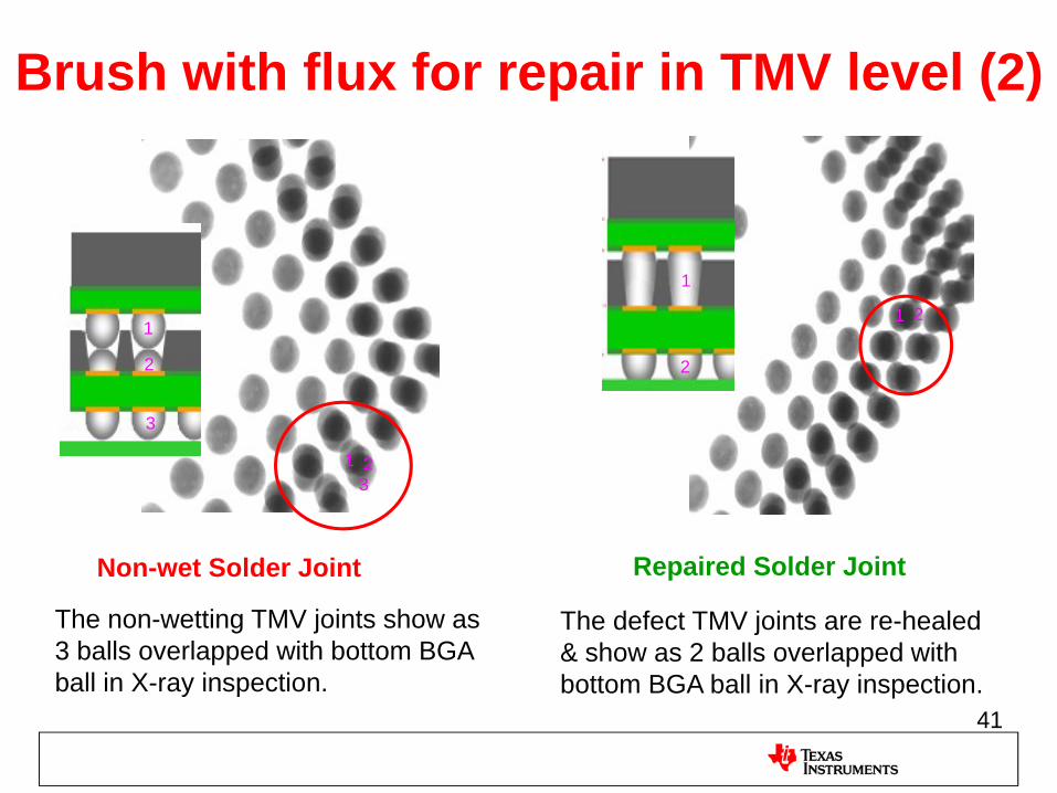
Brush with flux for repair in TMV level (2)
1
2
1 21
2
3
1 23
The non-wetting TMV joints show as 3 balls overlapped with bottom BGA ball in X-ray inspection.
The defect TMV joints are re-healed & show as 2 balls overlapped with bottom BGA ball in X-ray inspection.
Non-wet Solder Joint Repaired Solder Joint
42
AppendixA1: Through molded via solder rework methods
• Basic repair method• Manual rework methodNote: this method is not recommended for product repair due
to the number of times the topside solder ball is reflowedA2: X-ray examplesA3: Screen print material and reflow equipment examplesA4: Package warpage affect examples
43
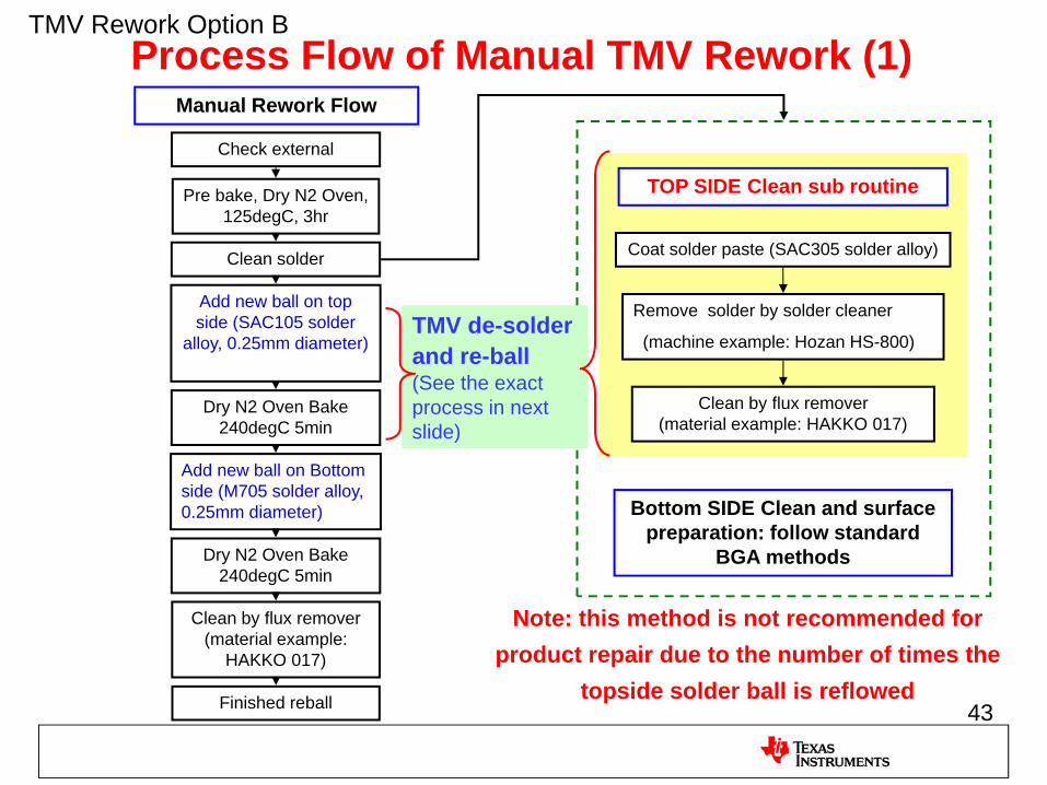
Check external
Clean solder
Pre bake, Dry N2 Oven, 125degC, 3hr
Add new ball on top side (SAC105 solder
alloy, 0.25mm diameter)
Dry N2 Oven Bake 240degC 5min
Add new ball on Bottom side (M705 solder alloy, 0.25mm diameter)
Finished reball
Coat solder paste (SAC305 solder alloy)
TOP SIDE Clean sub routine
Remove solder by solder cleaner
(machine example: Hozan HS-800)
Clean by flux remover (material example: HAKKO 017)
Bottom SIDE Clean and surface preparation: follow standard
BGA methods
Manual Rework Flow
Clean by flux remover (material example:
HAKKO 017)
Dry N2 Oven Bake 240degC 5min
TMV de-solder and re-ball(See the exact process in next slide)
Process Flow of Manual TMV Rework (1) TMV Rework Option B
Note: this method is not recommended for product repair due to the number of times the
topside solder ball is reflowed
44
Reball ApproachCustomer return
Solder up
De-soldering
Re-balling
Bake
Bottom reball process
• Thicker solder contributes better thermal conduction
• More flux help the solder soften and extract out , vacuum pressure ~80kPa
• Paint with flux and place 0.25mm solder ball and reflow
• measure coplanarity by an Equipment
Manual TMV Removal and Re-ball (2)
Solder up
TMV Rework Option B
45
AppendixA1: Through molded via solder rework methods
• Basic repair method• Manual rework method
A2: X-ray examplesA3: Screen print material and reflow equipment examples A4: Package warpage affect examples

46
Solder ball analysis by X-ray -1
Picture: POP and Memory mount on PCB. Before reflow.Solder paste printing check was good. Memory is mount on POP by fluxwith good accuracy.
1-pass reflow
47
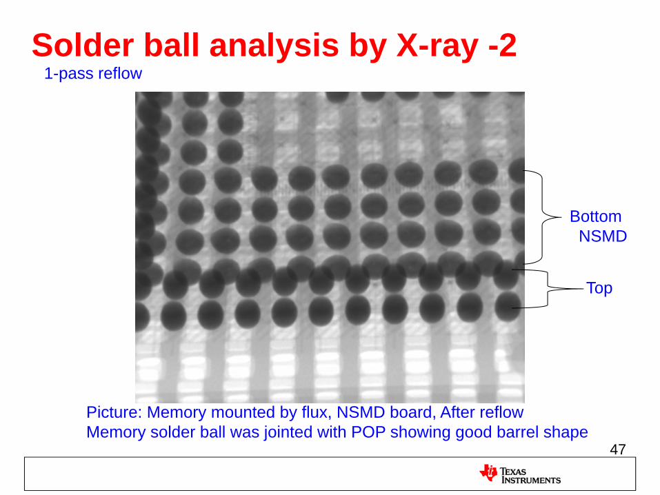
Solder ball analysis by X-ray -2
Picture: Memory mounted by flux, NSMD board, After reflowMemory solder ball was jointed with POP showing good barrel shape
BottomNSMD
Top
1-pass reflow
48
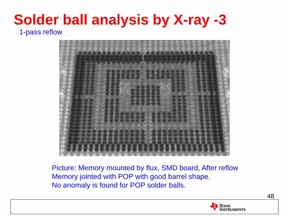
Solder ball analysis by X-ray -3
Picture: Memory mounted by flux, SMD board, After reflowMemory jointed with POP with good barrel shape. No anomaly is found for POP solder balls.
1-pass reflow
49
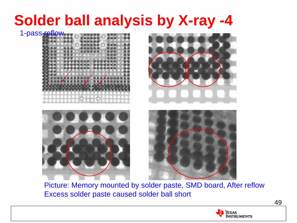
Solder ball analysis by X-ray -4
Picture: Memory mounted by solder paste, SMD board, After reflowExcess solder paste caused solder ball short
1-pass reflow
50
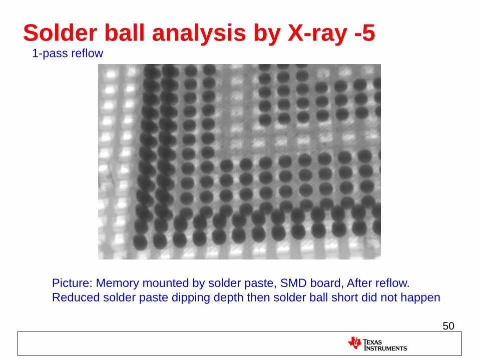
Solder ball analysis by X-ray -5
Picture: Memory mounted by solder paste, SMD board, After reflow.Reduced solder paste dipping depth then solder ball short did not happen
1-pass reflow
51
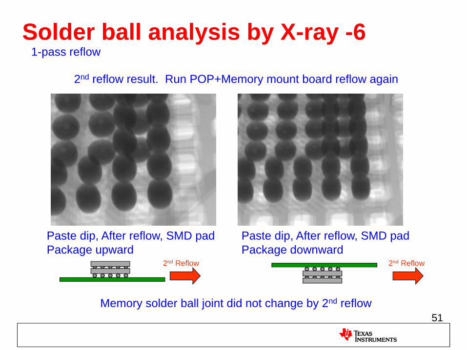
Solder ball analysis by X-ray -6
Paste dip, After reflow, SMD padPackage upward
Paste dip, After reflow, SMD padPackage downward
2nd reflow result. Run POP+Memory mount board reflow again
1-pass reflow
2nd Reflow2nd Reflow
Memory solder ball joint did not change by 2nd reflow

52
AppendixA1: Through molded via solder rework methods
• Basic repair method• Manual rework method
A2: X-ray examplesA3: Screen print material and reflow equipment examplesA4: Package warpage affect examples
53
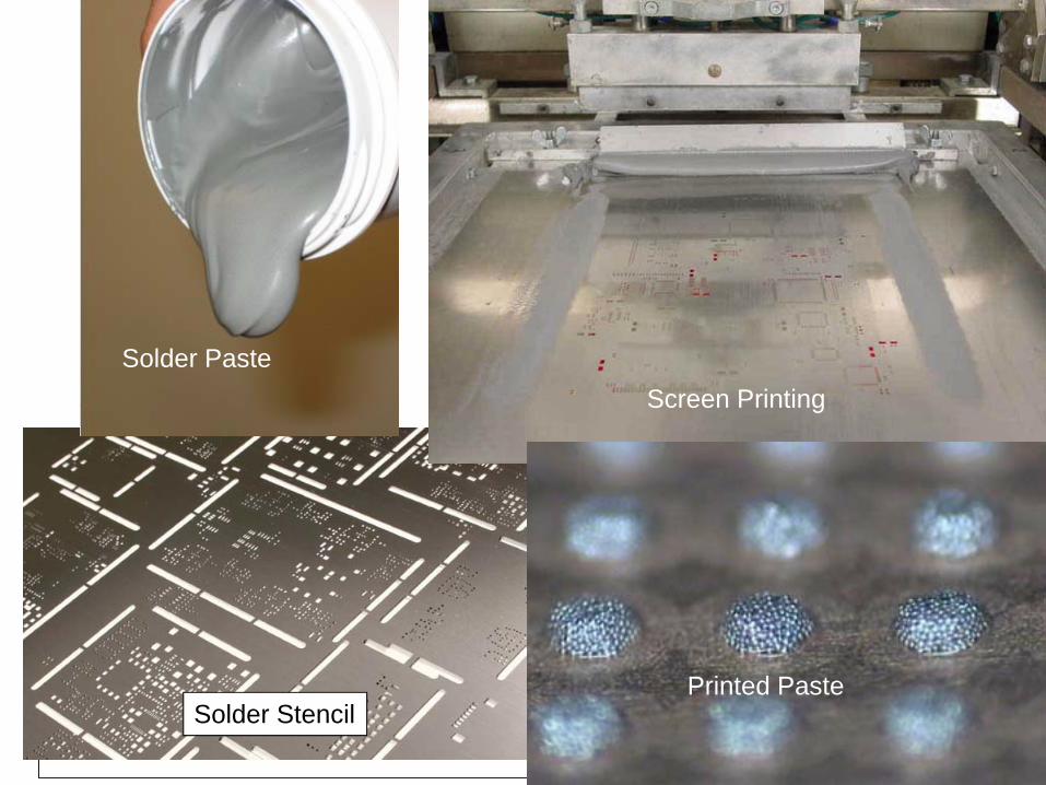
Solder PasteScreen Printing
Solder StencilPrinted Paste
54
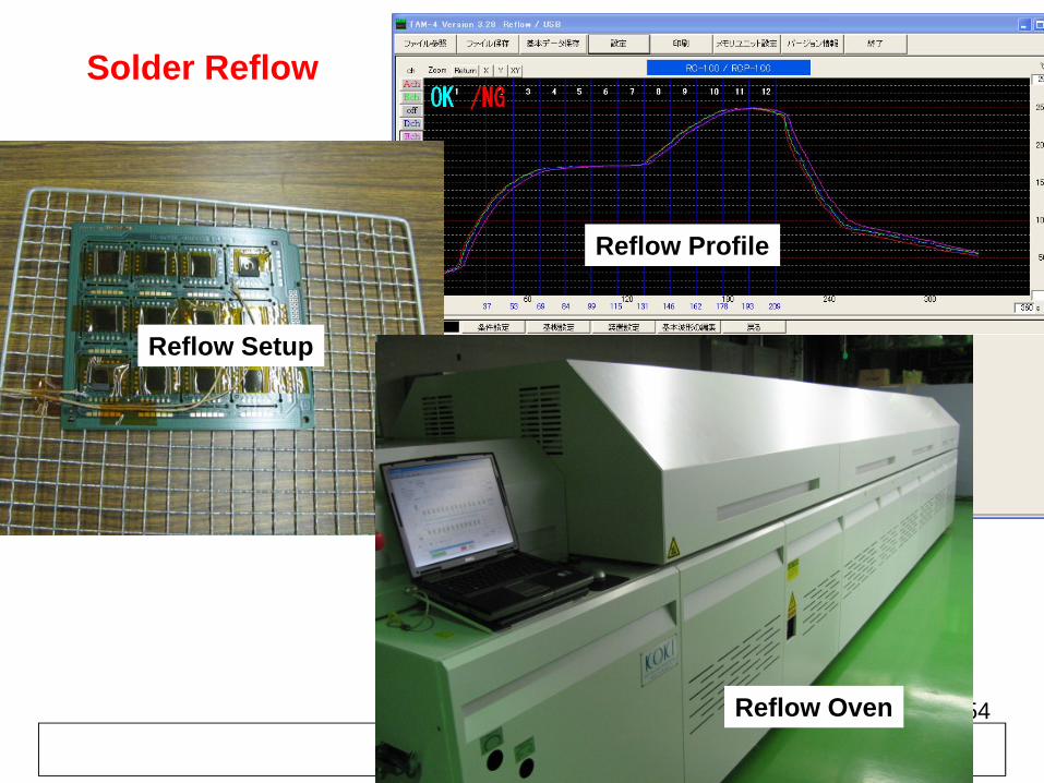
Reflow Profile
Reflow Setup
Solder Reflow
Reflow Oven
55
AppendixA1: Through molded via solder rework methods
• Basic repair method• Manual rework method
A2: X-ray examplesA3: Screen print material and reflow equipment examplesA4: Package warpage affect examples
56Sketches not to scale
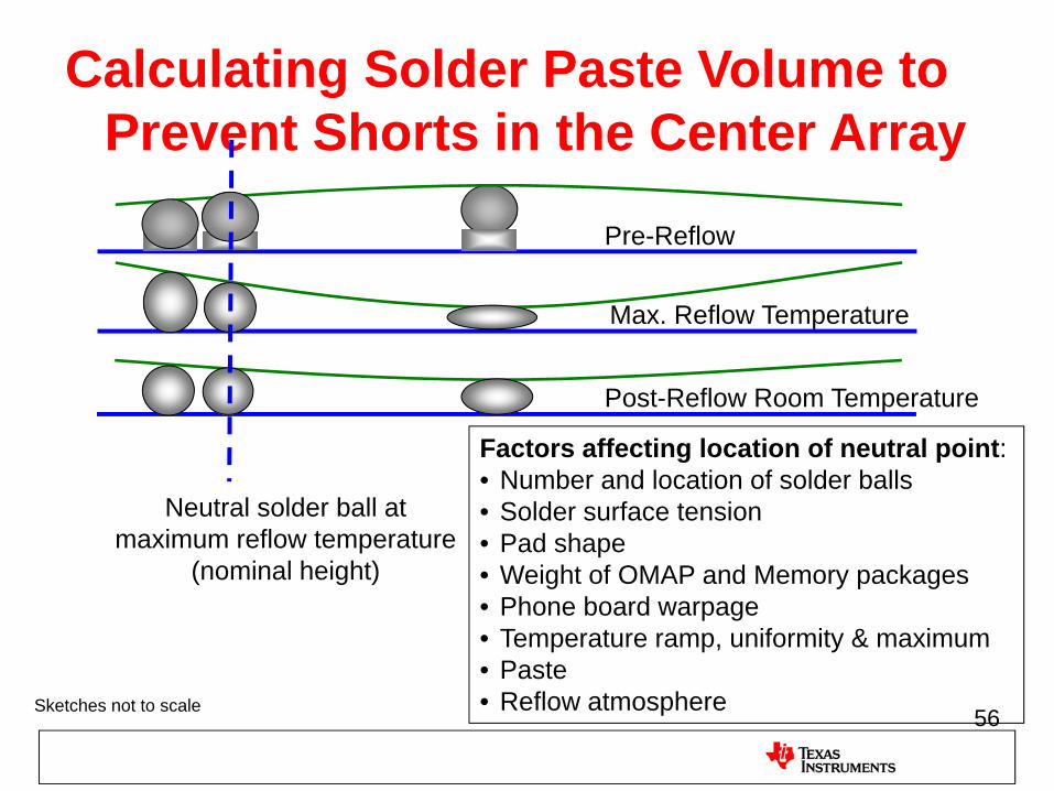
Calculating Solder Paste Volume to Prevent Shorts in the Center Array
Pre-Reflow
Max. Reflow Temperature
Post-Reflow Room Temperature
Neutral solder ball at maximum reflow temperature
(nominal height)
Factors affecting location of neutral point:• Number and location of solder balls• Solder surface tension• Pad shape• Weight of OMAP and Memory packages• Phone board warpage• Temperature ramp, uniformity & maximum• Paste• Reflow atmosphere
IMPORTANT NOTICE
Texas Instruments Incorporated and its subsidiaries (TI) reserve the right to make corrections, modifications, enhancements, improvements,and other changes to its products and services at any time and to discontinue any product or service without notice. Customers shouldobtain the latest relevant information before placing orders and should verify that such information is current and complete. All products aresold subject to TI’s terms and conditions of sale supplied at the time of order acknowledgment.
TI warrants performance of its hardware products to the specifications applicable at the time of sale in accordance with TI’s standardwarranty. Testing and other quality control techniques are used to the extent TI deems necessary to support this warranty. Except wheremandated by government requirements, testing of all parameters of each product is not necessarily performed.
TI assumes no liability for applications assistance or customer product design. Customers are responsible for their products andapplications using TI components. To minimize the risks associated with customer products and applications, customers should provideadequate design and operating safeguards.
TI does not warrant or represent that any license, either express or implied, is granted under any TI patent right, copyright, mask work right,or other TI intellectual property right relating to any combination, machine, or process in which TI products or services are used. Informationpublished by TI regarding third-party products or services does not constitute a license from TI to use such products or services or awarranty or endorsement thereof. Use of such information may require a license from a third party under the patents or other intellectualproperty of the third party, or a license from TI under the patents or other intellectual property of TI.
Reproduction of TI information in TI data books or data sheets is permissible only if reproduction is without alteration and is accompaniedby all associated warranties, conditions, limitations, and notices. Reproduction of this information with alteration is an unfair and deceptivebusiness practice. TI is not responsible or liable for such altered documentation. Information of third parties may be subject to additionalrestrictions.
Resale of TI products or services with statements different from or beyond the parameters stated by TI for that product or service voids allexpress and any implied warranties for the associated TI product or service and is an unfair and deceptive business practice. TI is notresponsible or liable for any such statements.
TI products are not authorized for use in safety-critical applications (such as life support) where a failure of the TI product would reasonablybe expected to cause severe personal injury or death, unless officers of the parties have executed an agreement specifically governingsuch use. Buyers represent that they have all necessary expertise in the safety and regulatory ramifications of their applications, andacknowledge and agree that they are solely responsible for all legal, regulatory and safety-related requirements concerning their productsand any use of TI products in such safety-critical applications, notwithstanding any applications-related information or support that may beprovided by TI. Further, Buyers must fully indemnify TI and its representatives against any damages arising out of the use of TI products insuch safety-critical applications.
TI products are neither designed nor intended for use in military/aerospace applications or environments unless the TI products arespecifically designated by TI as military-grade or "enhanced plastic." Only products designated by TI as military-grade meet militaryspecifications. Buyers acknowledge and agree that any such use of TI products which TI has not designated as military-grade is solely atthe Buyer's risk, and that they are solely responsible for compliance with all legal and regulatory requirements in connection with such use.
TI products are neither designed nor intended for use in automotive applications or environments unless the specific TI products aredesignated by TI as compliant with ISO/TS 16949 requirements. Buyers acknowledge and agree that, if they use any non-designatedproducts in automotive applications, TI will not be responsible for any failure to meet such requirements.
Following are URLs where you can obtain information on other Texas Instruments products and application solutions:
Products Applications
Audio www.ti.com/audio Communications and Telecom www.ti.com/communications
Amplifiers amplifier.ti.com Computers and Peripherals www.ti.com/computers
Data Converters dataconverter.ti.com Consumer Electronics www.ti.com/consumer-apps
DLP® Products www.dlp.com Energy and Lighting www.ti.com/energy
DSP dsp.ti.com Industrial www.ti.com/industrial
Clocks and Timers www.ti.com/clocks Medical www.ti.com/medical
Interface interface.ti.com Security www.ti.com/security
Logic logic.ti.com Space, Avionics and Defense www.ti.com/space-avionics-defense
Power Mgmt power.ti.com Transportation and Automotive www.ti.com/automotive
Microcontrollers microcontroller.ti.com Video and Imaging www.ti.com/video
RFID www.ti-rfid.com
OMAP Mobile Processors www.ti.com/omap
Wireless Connectivity www.ti.com/wirelessconnectivity
TI E2E Community Home Page e2e.ti.com
Mailing Address: Texas Instruments, Post Office Box 655303, Dallas, Texas 75265Copyright © 2011, Texas Instruments Incorporated