three-dimensional wiring for extensible quantum...
TRANSCRIPT

Three-Dimensional Wiring for Extensible Quantum Computing: The Quantum Socket
J. H. Béjanin,1,2 T. G. McConkey,1,3 J. R. Rinehart,1,2 C. T. Earnest,1,2 C. R. H. McRae,1,2 D. Shiri,1,2,† J. D. Bateman,1,2,‡
Y. Rohanizadegan,1,2 B. Penava,4 P. Breul,4 S. Royak,4 M. Zapatka,5 A. G. Fowler,6 and M. Mariantoni1,2,*1Institute for Quantum Computing, University of Waterloo,
200 University Avenue West, Waterloo, Ontario N2L 3G1, Canada2Department of Physics and Astronomy, University of Waterloo,
200 University Avenue West, Waterloo, Ontario N2L 3G1, Canada3Department of Electrical and Computer Engineering, University of Waterloo,
200 University Avenue West, Waterloo, Ontario N2L 3G1, Canada4INGUN Prüfmittelbau GmbH, Max-Stromeyer-Straße 162, D-78467 Konstanz, Germany
5INGUN USA, Inc., 252 Latitude Lane, Suite 102, Lake Wylie, South Carolina 29710-8152, USA6Google Inc., Santa Barbara, California 93117, USA
(Received 27 May 2016; revised manuscript received 7 August 2016; published 18 October 2016)
Quantum computing architectures are on the verge of scalability, a key requirement for theimplementation of a universal quantum computer. The next stage in this quest is the realization ofquantum error-correction codes, which will mitigate the impact of faulty quantum information on aquantum computer. Architectures with ten or more quantum bits (qubits) have been realized using trappedions and superconducting circuits. While these implementations are potentially scalable, true scalabilitywill require systems engineering to combine quantum and classical hardware. One technology demandingimminent efforts is the realization of a suitable wiring method for the control and the measurement of alarge number of qubits. In this work, we introduce an interconnect solution for solid-state qubits: thequantum socket. The quantum socket fully exploits the third dimension to connect classical electronics toqubits with higher density and better performance than two-dimensional methods based on wire bonding.The quantum socket is based on spring-mounted microwires—the three-dimensional wires—that pushdirectly on a microfabricated chip, making electrical contact. A small wire cross section (approximately1 mm), nearly nonmagnetic components, and functionality at low temperatures make the quantum socketideal for operating solid-state qubits. The wires have a coaxial geometry and operate over a frequency rangefrom dc to 8 GHz, with a contact resistance of approximately 150 mΩ, an impedance mismatch ofapproximately 10 Ω, and minimal cross talk. As a proof of principle, we fabricate and use a quantum socketto measure high-quality superconducting resonators at a temperature of approximately 10 mK. Quantumerror-correction codes such as the surface code will largely benefit from the quantum socket, which willmake it possible to address qubits located on a two-dimensional lattice. The present implementation of thesocket could be readily extended to accommodate a quantum processor with a (10 × 10)-qubit lattice,which would allow for the realization of a simple quantum memory.
DOI: 10.1103/PhysRevApplied.6.044010
I. INTRODUCTION
At present, one of the main objectives in the quantumcomputing community is to build prototypes of practicalhardware technology for scalable architectures that maylead to the realization of a universal quantum computer [1].In this work, we undertake the task of implementing anextensible wiring method for the operation of a quantum
processor based on solid-state devices, e.g., superconduct-ing qubits [2–4]. Possible experimental solutions based onwafer-bonding techniques [5–9] or coaxial through-siliconvias [10] as well as theoretical proposals [11,12] haverecently addressed the wiring issue, highlighting it as apriority for quantum computing.Building a universal quantum computer [13–18] will
make it possible to execute quantum algorithms [19], whichwould have profound implications on science and society.For a quantum computer to be competitive with the mostadvanced classical computer, it is widely believed that thequbit operations will require error rates on the order of 10−15
or less. Achieving such error rates is possible only by meansof quantum error-correction (QEC) algorithms [14,16,20],for example, the surface-code algorithm [21,22].
*Corresponding [email protected]
†Present address: Department of Physics, Chalmers Universityof Technology, SE-412 96 Göteborg, Sweden.
‡Present address: The Edward S. Rogers Sr. Department ofElectrical and Computer Engineering, University of Toronto, 10King’s College Road, Toronto, Ontario M5S 3G4, Canada.
PHYSICAL REVIEW APPLIED 6, 044010 (2016)
2331-7019=16=6(4)=044010(29) 044010-1 © 2016 American Physical Society
Quantum-computing architectures are based on effectivequantum-mechanical two-level systems, or physical qubits,which can be implemented using photons [23,24], trappedions [25], spins in molecules [26] and quantum dots[27–31], spins in silicon [30,32], and superconductingquantum circuits [2–4]. The last are leading the wayfor the realization of the first surface-code logical qubit,which will be implemented as an ensemble of a largenumber of physical qubits. Recently, several experimentsbased on superconducting quantum circuits demonstratedthe principles underlying the surface code. These worksshowed a complete set of physical gates with fidelitiesapproximately at the surface-code threshold [33], theparity measurements necessary to detect quantum errors[34,35], and realized a classical version of the surfacecode on a one-dimensional array of nine physical qubits[36]. Notably, the planar design inherent in the super-conducting qubit platform makes it possible to implementlarge two-dimensional qubit arrays, as required by thesurface code.Despite all of these accomplishments, a truly scalable
qubit architecture has yet to be demonstrated. Wiring is oneof the most basic unsolved scalability issues common tomost solid-state qubit implementations, where qubit arraysare fabricated on a chip. The conventional wiring methodbased on wire bonding suffers from fundamental scalinglimitations as well as mechanical and electrical restrictions.Wire bonding relies on bonding pads located at the edgesof the chip. Given a two-dimensional lattice of N × Nphysical qubits on a square chip, the number of wire bondsthat can be placed scales approximately as 4N (N bonds foreach chip side). Wire bonding will thus never be able toreach the required N2 law according to which physicalqubits scale on a two-dimensional lattice. Furthermore,for a large N, wire bonding precludes the possibility ofaccessing physical qubits in the center region of the chip,which is unacceptable for a physical implementation of thesurface code. In the case of superconducting qubits, forexample, qubit control and measurement are typicallyrealized by means of microwave pulses or, in general,pulses requiring large frequency bandwidths. By theirnature, these pulses cannot be reliably transmitted throughlong sections of quasifiliform wire bonds. In fact, straycapacitances and inductances associated with wirebonds—as well as the self-inductance of the bonditself—limit the available frequency bandwidth, thus com-promising the integrity of the control and measurementsignals [37].In this work, we set out to solve the wiring bottleneck
common to almost all solid-state qubit implementations.Our solution is based on suitably packaged three-dimensional microwires that can reach any area on a givenchip from above. We define this wiring system as thequantum socket. The wires are coaxial structures consistingof spring-loaded inner and outer conductors with diameters
of 380 and 1290 μm, respectively, at the smallest point andwith a maximum outer diameter of 2.5 mm. The movablesection of the wire is characterized by a maximum stroke ofapproximately 2.5 mm, allowing for a wide range of on-chip mechanical compressions. All wire components arenearly nonmagnetic, thereby minimizing any interferencewith the qubits. The three-dimensional wires work both atroom temperature and at cryogenic temperatures as low asapproximately 10 mK. The wires’ test-retest reliability(repeatability) is excellent, with marginal variability overhundreds of measurements. Their electrical performance isgood from dc to at least 8 GHz, with a contact resistancesmaller than 150 mΩ and an instantaneous impedancemismatch of approximately 10 Ω. Notably, the coaxialdesign of the wires strongly reduces unwanted cross talk,which we measured to be, at most, −45 dB for a realisticquantum-computing application.This article is organized as follows. In Sec. II, we
introduce the quantum-socket design and microwave sim-ulations. In Sec. III, we show the socket physical imple-mentation, with emphasis on materials and alignmentprocedures. In Sec. IV, we present a comprehensive dcand microwave characterization of the quantum-socketoperation at room and cryogenic temperatures. In Sec. V,we show an application of the quantum socket relevant tosuperconducting quantum computing, where the socket isused to measure aluminum (Al) superconducting resonatorsat a temperature of approximately 10 mK. Finally, inSec. VI, we envision an extensible quantum-computingarchitecture where a quantum socket is used to connect to a10 × 10 lattice of superconducting qubits.
II. THE QUANTUM-SOCKET DESIGN
The development of the quantum socket requires a stageof meticulous micromechanical and microwave design andsimulations. It is determined that a spring-loaded inter-connect—the three-dimensional wire—is the optimalmethod to electrically access devices lithographicallyfabricated on a chip [38] and operated in a cryogenicenvironment. An on-chip contact pad geometrically andelectrically matched to the bottom interface of the wire canbe placed easily at any desired location on the chip as partof the fabrication process, thus making it possible toreach any point on a two-dimensional lattice of qubits.The coaxial design of the wire provides a wideoperating frequency bandwidth, while the springs allowfor mechanical stress relief during the cooling process. Thethree-dimensional wires used in this work take advantageof the knowledge in the existing field of microwave-circuittesting [39]. However, reducing the wire dimensions to afew hundred micrometers and using it to connect toquantum-mechanical microfabricated circuits at low tem-peratures results in a significant extension of existingimplementations and applications.
J. H. BÉJANIN et al. PHYS. REV. APPLIED 6, 044010 (2016)
044010-2

A. Three-dimensional wires
Figure 1 shows the design of the quantum-socketcomponents. Figure 1(a) displays a model of a three-dimensional wire. The coaxial design of the wire is visiblefrom the image, which features a wire that is 30.5 mm long
when uncompressed. The wire is characterized by an innercylindrical pin with a diameter of 380 μm and an outercylindrical body (the electrical ground) with a diameter of1290 μm in its narrowest region; this region is the bottom-most section of the wire and, hereafter, will be referred to as
(a)
(b)
(d)
FIG. 1. Computer-aided designs of the three-dimensional wire, microwave package, and package holder. (a) A wire of lengthl ¼ 30.5 mm along with a detail of the contact head (inset). (b) Assembled microwave package including six three-dimensional wires,washer, washer springs, and chip (shown in green). The arrow indicates the screw-in microconnector mated to the back end of thewire. Forward hatching indicates the washer cutaway, whereas backward hatching indicates both lid and sample-holder cutaways.(c) Cross section of the microwave package showing the height of the upper cavity, which coincides with the minimum compressiondistance lc of the three-dimensional wires (see Appendix A). (d) Microwave package mounted to the package holder, connected, in turn,to the mounting plate of a DR with SMP connectors. A channel with a cross-sectional area of 800 × 800 μm2 connects the inner cavitiesof the package to the outside, thus making it possible to evacuate the inner compartments of the package. This channel meanders toprevent external electromagnetic radiation from interfering with the sample.
THREE-DIMENSIONAL WIRING FOR EXTENSIBLE … PHYS. REV. APPLIED 6, 044010 (2016)
044010-3

the wire contact head [see the inset of Fig. 1(a), as well asthe dashed box on the left side of Fig. 2(a)]. The contacthead terminates at the wire bottom interface; this interfaceis designed to mate with a pad on a chip [see Figs. 2(b)and 2(c)]. The outer body includes a rectangular aperture,the tunnel, to prevent shorting the inner conductor of an on-chip coplanar-waveguide (CPW) transmission line [40,41];the transmission line can connect the pad with any otherstructure on the chip. Two different tunnel dimensions aredesigned, with the largest one reducing potential alignmenterrors [42]. The tunnel height is 300 μm in both cases, witha width of 500 or 650 μm. The internal spring mechanismsof the wire allow the contact head to be compressed; themaximum stroke is designed to be 2.5 mm, correspondingto a working stroke of 2.0 mm.The outer body of the three-dimensional wire is an M2.5
male thread used to fix the wire to the lid of the microwavepackage [see Figs. 1(b) and 1(d)]. The thread is split intotwo segments 3.75 and 11.75 mm long that are separatedby a constriction with an outer diameter of 1.90 mm. Theconstriction is necessary to assemble and maintain in placethe inner components of the three-dimensional wire. Alaser-printed marker is engraved into the top of the outerbody. The marker is aligned with the center of the tunnel,making it possible to mate the wire bottom interface with apad on the underlying chip with a high degree of angularprecision.
Figure 2(a) shows a lateral two-dimensional cut view ofthe three-dimensional wire. Two of the main wire compo-nents are the inner and outer barrels, which compose part ofthe inner and outer conductors. The inner-conductor barrelis a hollow cylinder with outer and inner diameters of 380and 290 μm [indicated as part iv in Fig. 2(a)], respectively.This barrel encapsulates the inner-conductor spring. Theouter-conductor barrel is a hollow cylinder as well, in thiscase with an inner diameter of 870 μm [Figs. 2(a) part ii and2(a) part vii]. Three polytetrafluoroethylene (PTFE) disksserve as spacers between the inner and outer conductors;such disks contribute marginally to the wire dielectricvolume, the majority of which is air or vacuum. The outerspring is housed within the outer barrel towards its backend, just before the last PTFE disk on the right-hand side ofthe wire. The back end of the wire is a region comprising afemale thread on the outer conductor and an inner-conductor barrel [see the dashed box on the right-handside of Fig. 2(a)].The inner-conductor tip is characterized by a conical
geometry with an opening angle of 30°. Such a sharp designis chosen to ensure that the tip would pierce through anypossible oxide layer forming on the contact-pad metallicsurface, thus allowing for a good electrical contact.Figure 2(c) shows the design of a typical on-chip pad
used to make contact with the bottom interface of a three-dimensional wire. The pad comprises an inner and an outer
(a)
(b) (c) (d)
FIG. 2. Two-dimensional cut view of the three-dimensional wire, contact pad, and screw-in microconnector. (a) Side view of the wirecross section. The wire components are i spring-loaded center conductor of the contact head; ii spring-loaded outer conductor of thecontact head; iii, vi, and ix dielectric spacers; iv center-conductor barrel; v center-conductor spring; vii outer-conductor barrel; viii outer-conductor spring; x center-conductor tail; xi outer-conductor tail; and xii threaded outer body. The dashed box on the left indicates thecontact head, whereas that on the right indicates the female threads included for use with the screw-in microconnector. (b) Front view ofthe wire. The blue surface indicates the wire bottom interface. (c) On-chip contact pad. Here, the blue surface indicates the pad dielectricgap, whereas the white surfaces refer to conductors (thin metallic films deposited on a dielectric substrate). (d) Screw-in microconnector.The left end of the microconnector mates with the back end of the three-dimensional wire; the right end is soldered to a coaxial cable, theinner conductor of which serves as the inner conductor of the microconnector (slotting into x).
J. H. BÉJANIN et al. PHYS. REV. APPLIED 6, 044010 (2016)
044010-4

conductor, with the outer conductor being grounded. Thepad in the figure is designed for a silver (Ag) film with athickness of 3 μm. A variety of similar pads are designedfor gold (Au) and Al films with a thickness rangingbetween approximately 100 and 200 nm. The pad innerconductor is a circle with a diameter of 320 μm thatnarrows to a linear trace (i.e., the inner conductor of aCPW transmission line) by means of a raised-cosine taper.The raised cosine makes it possible to maximize the padarea while minimizing impedance mismatch. As designed,the wire and the pad allow for lateral and rotationalmisalignments of ∓140 μm and ∓28°, respectively. Thesubstrate underneath the pad is assumed to be silicon (Si)with a relative electric permittivity of ϵr ≃ 11. The dielec-tric gap between the inner and outer conductors is 180 μmin the circular region of the pad; the outer edge of thedielectric gap then follows a similar raised-cosine taper asthe inner conductor. The pad’s characteristic impedance isdesigned to be Zc ¼ 50 Ω.
B. Microwave package
The microwave package comprises three main parts: thelid, the sample holder, and the grounding washer. Thepackage is a parallelepiped with a height of 30 mm and witha square base having a side length of 50 mm. The chip ishoused inside the sample holder. All of these componentsmate as shown in Figs. 1(b) and 1(c).In order to connect a three-dimensional wire to a device
on a chip, the wire is screwed into an M2.5 female threadthat is tapped into the lid of the microwave package, asdepicted in Fig. 1(b). The pressure applied by the wire tothe chip is set by the depth of the wire in the package.The wire stroke, package dimensions, thread pitch, andalignment constraints impose discrete pressure settings(see Appendix A). In the present implementation of thequantum socket, the lid is designed to hold a set of sixthree-dimensional wires, which are arranged in two parallelrows. In each row, the wires are spaced 5.75 mm fromcenter to center, with the two rows being separated by adistance of 11.5 mm.A square chip of lateral dimensions 15 × 15 mm2 is
mounted in the sample holder in a similar fashion as inRef. [43]. The outer edges of the chip rest on four protrudinglips, which are 1 mm wide. Hereafter, those lips will bereferred to as the chip recess. For design purposes, a chipthickness of 550 μm is assumed. Correspondingly, the chiprecess is designed so that the top of the chip protrudes by100 μm with respect to the adjacent surface of the chipholder, i.e., the depth of the recess is 450 μm [see Fig. 1(c)].The outer edges of the chip are pushed on by a spring-loadedgrounding washer. The 100-μm chip protrusion ensures agood electrical connection between chip and washer, asshown in Fig. 1(c).The grounding washer is designed to substitute the large
number of lateral bonding wires that would otherwise be
required to provide a good ground to the chip (as shown, forexample, in Fig. 6 of Ref. [43]). The washer springs arevisible in Fig. 1(b), which also shows a cut view of thewasher. The washer itself is electrically grounded by meansof the springs as well as through galvanic connection to thesurface of the lid. The four feet of the washer, which can beseen in the cut view of Fig. 1(b), can be designed to beshorter or longer. This flexibility makes it possible tochoose different pressure settings for the washer.After assembling the package, there exist two electrical
cavities [see Fig. 1(c)]: one above the chip, formed by thelid, washer, and metallic surface of the chip (the uppercavity), and one below the chip, formed by the sampleholder and metallic surface of the chip (the lower cavity).The hollow cavity above the chip surface has the dimen-sions 14 × 14 × 3.05 mm3. The dimensions of the cavitybelow the chip surface are 13 × 13 × 2 mm3. The lowercavity helps mitigate any parasitic capacitance between thechip and the box (the ground). Additionally, it serves tolower the effective electric permittivity in the region belowthe chip surface, increasing the frequency of the substratemodes (see Sec. II D).A pillar of a square cross section with a side length of
1 mm is placed right below the chip at its center; the pillartouches the bottom of the chip, thus providing mechanicalsupport [44]. The impact of such a pillar on the microwaveperformance of the package is described in Sec. II D.
C. Package holder
The three-dimensional wires, which are screwed into themicrowave package, must be connected to the qubit controland measurement electronics. In addition, for cryogenicapplications, the package must be thermally anchored to arefrigeration system in order to be cooled to the desiredtemperature. Figure 1(d) shows the mechanical modulewe designed to perform both electrical and thermal con-nections. In this design, each three-dimensional wire isconnected to a screw-in microconnector, which is indicatedby an arrow in Fig. 1(b) and is shown in detail in Fig. 2(d).One end of the microconnector comprises a male threadand an inner-conductor pin that mate with the back end ofthe three-dimensional wire. The other end of the micro-connector is soldered to a coaxial cable [45].The end of each coaxial cable opposite to the corre-
sponding three-dimensional wire is soldered to a subminia-ture push-on (SMP) connector. The SMP connectors arebolted to a horizontal plate attached to the microwavepackage by means of two vertical fixtures, as shown inFig. 1(d). The vertical fixtures and the horizontal plateconstitute the package holder. The package holder and themicrowave package form an independent assembly. Ahorizontal mounting plate, designed to interface with thepackage holder, houses a set of matching SMP connectors.The mounting plate is mechanically and, thus, thermally
THREE-DIMENSIONAL WIRING FOR EXTENSIBLE … PHYS. REV. APPLIED 6, 044010 (2016)
044010-5

anchored to the mixing chamber (MC) stage of a dilutionrefrigerator (DR).
D. Microwave simulations
The three-dimensional wires, the 90° transition betweenthe wire and the on-chip pad, and the inner cavities of afully assembled microwave package are extensively simu-lated numerically at microwave frequencies [46]. Theresults for the electromagnetic field distribution at afrequency of approximately 6 GHz, which is a typicaloperation frequency for superconducting qubits, are shownin Fig. 3. Figure 3(a) shows the field behavior for a barethree-dimensional wire. The field distribution resemblesthat of a coaxial transmission line except for noticeableperturbations at the dielectric PTFE spacers. Figure 3(b)shows the 90° transition region. This region is critical forsignal integrity since abrupt changes in physical geometrycause electrical reflections [39,48]. In order to minimizesuch reflections, an impedance-matched pad is designed.However, this design leads to a large electromagneticvolume in proximity to the pad, as seen in Fig. 3(b),possibly resulting in parasitic capacitance and cross talk.In addition to considering the wire and the transition
region, the electrical behavior of the inner cavities of thepackage is studied analytically and simulated numerically.As described in Sec. II B, the metallic surface of the chipeffectively divides the cavity of the sample holder into two
regions: a vacuum cavity above the metal surface and acavity partially filled with a dielectric below the metalsurface. The latter is of greater concern, as the dielectricacts as a perturbation to the cavity vacuum [49], thuslowering the box modes. For a simple rectangular cavity,the frequency f of the first mode due to this perturbationcan be found as [41]
f ¼ f0 −f0ðϵr − 1Þds
2b; ð1Þ
where f0 is the frequency of the unperturbed mode, ϵr therelative electric permittivity of the dielectric, ds the sub-strate thickness, and b the cavity height. From Eq. (1), weestimate this box mode to be 12.8 GHz. However, con-sidering the presence of the pillar, the three-dimensionalwires, etc., we have to use numerical simulations to obtain amore accurate estimate of the lowest box modes. Theresults for the first three modes are reported in Table I.Discounting the pillar, the analytical and simulated valuesare in good agreement with each other. The addition ofthe support pillar significantly lowers the frequency of themodes. In fact, it increases the relative filling factor of thecavity by confining more of the electromagnetic field tothe dielectric than to the vacuum. Given the dimensions ofthis design, the pillar leads to a first mode which couldinterfere with typical qubit frequencies. In spite of this
(a)
(b) (c)
FIG. 3. Numerical simulations of the electric field distribution. (a) Field for a three-dimensional wire at 6 GHz. (b) Field in proximityto the 90° transition region, also at 6 GHz. (c) Field for the first box mode at 6.3 GHz. Color-bar scales are indicated in their respectivepanels. The x, y, and z directions of a Cartesian coordinate system are also indicated. In (b), the cross section of the transition region isshown. Note the large volume occupied by the electric field beneath the contact pad. In (c), an offset cross section of the first box mode isshown. The field confinement due to the pillar is clearly visible. Additionally, the simulation shows a slight field confinement in theregion surrounding the chip recess. A time-domain animation of the simulated electric field distributions can be found in Sec. S3 of theSupplemental Material [47].
J. H. BÉJANIN et al. PHYS. REV. APPLIED 6, 044010 (2016)
044010-6

possibility, the pillar is included in the design in orderto provide a degree of mechanical support. Note that thepillar can alternatively be realized as a dielectric material,e.g., PTFE; a dielectric pillar would no longer cause fieldconfinement between the top surface of the pillar and themetallic surface of the chip.
III. IMPLEMENTATION
The physical implementation of the main components ofthe quantum socket is displayed in Fig. 4. In particular,Fig. 4(a) shows a macrophotograph of a three-dimensionalwire. The inset shows a scanning electron microscope(SEM) image of the wire contact head, featuring the500-μm version of the tunnel. This wire is cycled approx-imately ten times; as a consequence, the center conductor of
TABLE I. Simulation results for the first three box modes of thelower cavity inside the assembled microwave package shown inFig. 1(b). The dielectric used for these simulations is Si at roomtemperature with a relative electric permittivity of ϵr ¼ 11.68.“Vacuum” indicates that no Si is present in the simulation, while“with pillar” indicates that the ð1.0 × 1.0 × 2.0Þ-mm3 supportpillar is present. TExyz indicates the number of half wavelengthsspanned by the electric field in the x, y, and z directions,respectively [see Fig 3(c)]. Note that the frequency of the firstmode of the upper cavity is approximately 17.2 GHz.
TE110 (GHz) TE120 (GHz) TE210 (GHz)
Vacuum 15.7 24.2 24.2Vacuum with pillar 13.1 23.6 23.6Si 13.5 16.8 16.8Si with pillar 6.3 16.2 16.9
FIG. 4. Images of the quantum socket as implemented. (a) Macrophotograph of a three-dimensional wire. (Inset) SEM image of thecontact head. The wire components are machined by means of a high-precision screw-type mill. Note that the tip of the inner conductorretains small metallic flakes that are scraped off the on-chip pads. (b) Microwave package lid with six three-dimensional wires and fourwasher springs, washer, and sample holder with chip installed. (c) Package holder with attached microwave package mounted to the MCstage of a DR. The lid of a custom-made magnetic shield can be seen at the top of the panel.
THREE-DIMENSIONAL WIRING FOR EXTENSIBLE … PHYS. REV. APPLIED 6, 044010 (2016)
044010-7
the contact head, which had a conical, sharp shapeoriginally, flattens at the top. The metallic componentsof the wire are made from bronze and brass (see Sec. III A),and all springs from hardened beryllium copper (BeCu).Except for the springs, all of the components are goldplated, without any nickel (Ni) adhesion underlayer.Figure 4(b) displays the entire microwave package in the
process of locking the package lid and sample holdertogether, with a chip and grounding washer alreadyinstalled. As shown in the figure, two rows of three-dimensional wires, for a total number of six wires, arescrewed into the lid with pressure settings as described inAppendix A; each wire is associated with one on-chipCPW pad. The four springs that mate with the grounding-washer feet are embedded in corresponding recesses in thelid; the springs are glued in these recesses by way of amedium-strength thread locker that is tested at low temper-atures. Figure 4(c) shows a picture of the assembledmicrowave package attached to the package holder; theentire structure is attached to the MC stage of a DR. Moredetails about materials and microwave components can befound in Sec. S2 of the Supplemental Material [47].
A. Magnetic properties
An important stage in the physical implementation ofthe quantum socket is the choice of materials to be usedfor the three-dimensional wires. In fact, it has been shownthat nonmagnetic components in proximity of supercon-ducting qubits are critical to preserve long qubit coherence[50–53]. The three-dimensional wires are the closestdevices to the qubits. For this reason, all of theircomponents should be made using nonmagnetic materials.Because of machining constraints, however, alloys con-taining ferromagnetic impurities [iron (Fe), cobalt (Co),and Ni] have to be used. For the outer-conductor compo-nents, we use brass, which is easy to thread; the chosentype is CW724R [54]. For the inner-conductor compo-nents, brass CW724R does not meet the machiningrequirements. Consequently, we decide to use copperalloy (phosphor bronze) CW453K [55]. The chemicalcomposition for these two materials is reported inTable IV of Appendix B. The dielectric spacers are madefrom PTFE and the rest of the components from hardenedBeCu; both materials are nonmagnetic. The weightpercentage of ferromagnetic materials is non-negligiblefor both CW453K and CW724R. Thus, we perform aseries of tests using a zero-Gauss chamber (ZGC) in orderto ensure that both materials are sufficiently nonmagnetic.The results are given in Appendix B and show that themagnetic impurities should be small enough not to disturbthe operation of superconducting quantum devices.The microwave package and the grounding washer are
made from high-purity Al alloy 5N5 (99.9995% purity).The very low level of impurities in this alloy assuresminimal stray magnetic fields generated by the package and
the washer, as confirmed by the magnetic tests discussed inAppendix B.
B. Thermal properties
The thermal conductance of the three-dimensional wiresis a critical parameter to be analyzed for the interconnectionwith devices at cryogenic temperatures. Low thermalconductivity would result in poor cooling of the devices,which, in the case of qubits, may lead to an incoherentthermal mixture of the qubit ground state jgi and theexcited state jei [56,57]. Even a slightly mixed state wouldsignificantly deteriorate the fidelity of the operationsrequired for QEC [58]. It has been estimated that someof the qubits in the experiment of Ref. [36], which reliessolely on Al-wire bonds as a means of thermalization, arecharacterized by an excited-state population Pe ≃ 0.04.Among other possible factors, it is believed that thispopulation is due to the poor thermal conductance of theAl-wire bonds. In fact, these bonds become superconduc-tive at the desired qubit operation temperature of approx-imately 10 mK, preventing the qubits from thermalizingand, thus, from being initialized in jgi with high fidelity.In order to compare the thermal performance of an
Al-wire bond with that of a three-dimensional wire, weestimate the heat-transfer rate per kelvin of a wire,Πt, usinga simplified coaxial geometry. At a temperature of 25 mK,we calculate Πt ≃ 6 × 10⁻⁷ WK−1. At the same temper-ature, the heat-transfer rate per kelvin of a typical Al-wirebound is estimated to be Πb ≃ 4 × 10⁻¹² WK−1 (seeAppendix C for more details). A very large number ofAl-wire bonds would thus be required to obtain athermal performance comparable to that of a singlethree-dimensional wire.
C. Spring characterization
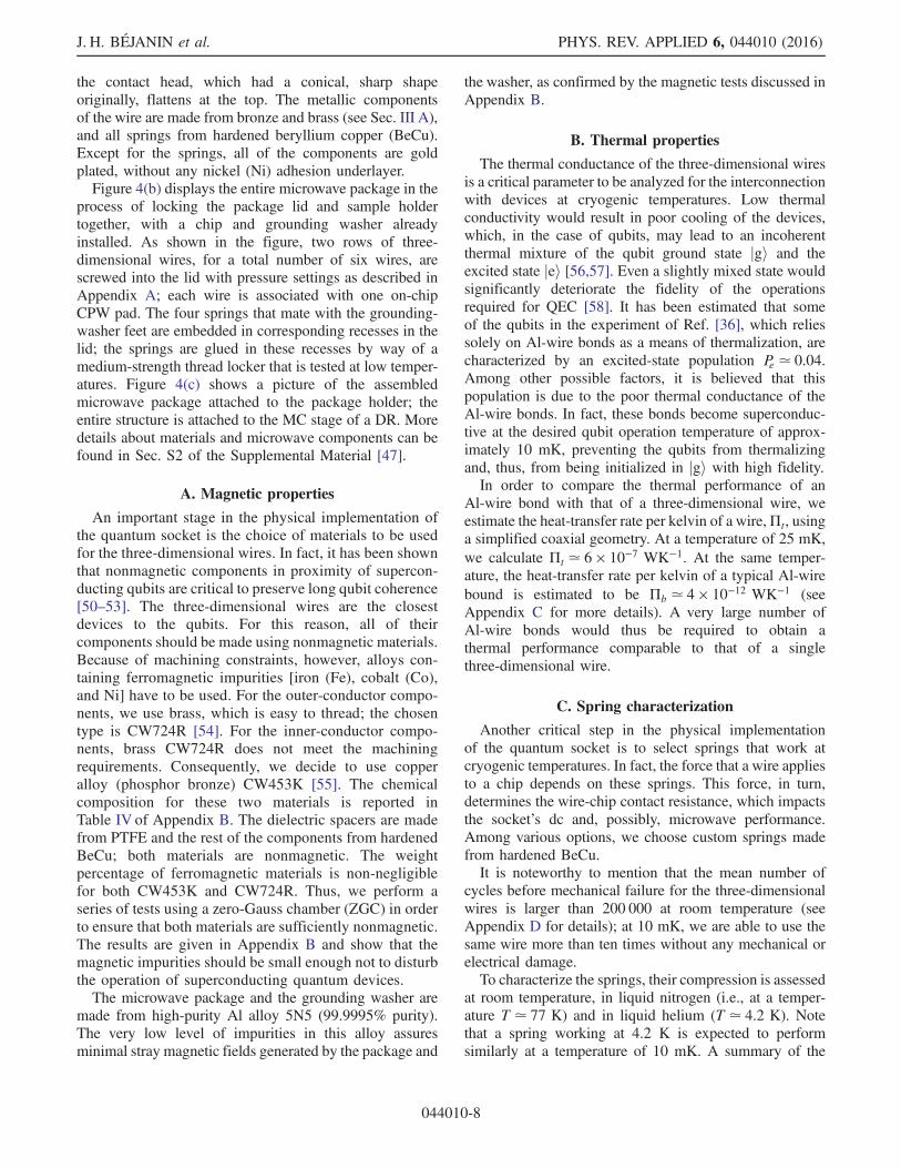
Another critical step in the physical implementationof the quantum socket is to select springs that work atcryogenic temperatures. In fact, the force that a wire appliesto a chip depends on these springs. This force, in turn,determines the wire-chip contact resistance, which impactsthe socket’s dc and, possibly, microwave performance.Among various options, we choose custom springs madefrom hardened BeCu.It is noteworthy to mention that the mean number of
cycles before mechanical failure for the three-dimensionalwires is larger than 200 000 at room temperature (seeAppendix D for details); at 10 mK, we are able to use thesame wire more than ten times without any mechanical orelectrical damage.To characterize the springs, their compression is assessed
at room temperature, in liquid nitrogen (i.e., at a temper-ature T ≃ 77 K) and in liquid helium (T ≃ 4.2 K). Notethat a spring working at 4.2 K is expected to performsimilarly at a temperature of 10 mK. A summary of the
J. H. BÉJANIN et al. PHYS. REV. APPLIED 6, 044010 (2016)
044010-8

thermomechanical tests is reported in Appendix D. Themain conclusion of the tests is that the springs do not break(even after numerous temperature cycles) and have similarspring constants at all measured temperatures.
D. Alignment
In order to implement a quantum socket with excellentinterconnectivity properties, it is imperative to minimizemachining errors and mitigate the effects of any residualerrors. These errors are mainly due to dicing tolerances,tapping tolerances of the M2.5-threaded holes of the lid,tolerances of the mating parts for the inner cavities of the lidand sample holder, and tolerances of the chip recess. Theseerrors can cause both lateral and rotational misalignmentand likely become worse when cooling the quantum socketto low temperatures. More details on alignment errors canbe found in Appendix E.The procedure to obtain an ideal and repeatable align-
ment comprises three main steps: optimization of thecontact pad and tunnel geometry, accurate and precisechip dicing, and accurate and precise package machining.For the quantum socket described in this work, the optimaltunnel width is found to be 650 μm. This tunnel widthmaintains reasonable impedance matching, while allowinggreater CPW contact-pad and tapering dimensions. Thecontact-pad width Wp and taper length Tp are chosen to beWp ¼ 320 μm and Tp ¼ 360 μm. These dimensions are themaximum ones allowable for accommodating the geometryof the wire bottom interface for a nominal lateral androtational misalignment of ∓140 μm and ∓28°, respec-tively. In order to select the given pad dimensions, we hadto resort to a 50-Ω matched raised-cosine tapering.A majority of the chips used in the experiments pre-
sented here are diced with a dicing saw from the DISCOCorporation (model DAD3240). To obtain a desired dielength, both the precision of the saw-stage movementand the blade’s kerf have to be considered. For theDAD3240 saw, the former is approximately 4 μm, whereasthe latter changes with usage and materials. For the highestaccuracy cut, we measure the kerf on the same type ofwafer just prior to cutting the actual die. In order to achievemaximum benefit from the saw, rotational- and lateral-alignment dicing markers are incorporated on the wafer.Such a meticulous chip-dicing procedure is only effectivein conjunction with a correspondingly high level ofmachining accuracy and precision. We used standardcomputer-numerical-control machining with a toleranceof 1 thou (25.4 μm), although electrical-discharge machin-ing can be pursued if more stringent tolerances (≲10 μm)are required.Following the aforementioned procedures, we are able
to achieve the desired wire-pad matching accuracy andprecision, which results in a repeatability of 100% over 94instances. These figures of merit are tested in two steps:first, by microimaging several pads that are mated to a
three-dimensional wire (see Sec. III D 1) and, second, bymeans of dc-resistance tests (see Sec. III D 2).
1. On-chip pad microimaging
Microimaging is performed on a variety of differentsamples, four of which are exemplified in Fig. 5. The figureshows a set of microimages for Ag and Al pads (detailsregarding the fabrication of these samples are available inAppendix F). Figures 5(a) and 5(b) show two Ag pads thatare mated with the three-dimensional wires at room temper-ature. Figure 5(a) shows a mating instance where thewire bottom interface perfectly matches the on-chip pad.Figure 5(b) shows two mating instances that, even thoughnot perfectly matched, remain within the designed toler-ances. Notably, simulations of imperfect mating instancesrevealed that an off-centered wire does not significantly
(b) (d)
(a) (c)
FIG. 5. Microimages used to evaluate the alignment procedureof the three-dimensional wires. (a),(b) Ag pads. The magentaarrows indicate the first (1) and second (2) mating instance.The lengths Wp and Tp are indicated in (a) by means of magentadouble arrows. (c),(d) Al pad before and after a cooling cycle toapproximately 10 mK. Center conductor dragging due to coolingis indicated by a green double arrow. The magenta (thick) dashedline in (a) indicates tunnel (i.e., rotational) alignment for the Agpad. Note that the geometries for the pads in (a) and (b) areoptimized for a 3-μmAg film and, thus, are slightly different thanthose for the pads in (c) and (d), which are designed for a 120-nmAl film.
THREE-DIMENSIONAL WIRING FOR EXTENSIBLE … PHYS. REV. APPLIED 6, 044010 (2016)
044010-9

affect the microwave performance of the quantum socket.Finally, Figs. 5(c) and 5(d) display two Al pads which areboth mated with a wire one time.While the pad in Fig. 5(c) isoperated only at room temperature, the pad in Fig. 5(d) ispart of an assembly that is cooled to approximately 10 mKfor about three months. The image is taken after theassembly is cycled back to room temperature and showsa dragging of the wire by a few tens of micrometers. Such adisplacement can likely be attributed to the difference in thethermal expansion of Si and Al (see Appendix E).As a diagnostic tool, microimages of a sample already
mounted in the sample holder after a mating cycle can beobtained readily by means of a handheld digital microscope.
2. dc-resistance tests
In contrast to the microimaging tests, which require theremoval of the microwave package’s lid, dc-resistance testscan be performed in situ at room temperature after thepackage and the package holder have been fully assembled.These tests are performed on all devices presented in thiswork, including the Au, Ag, and Al samples.The typical test setup comprises a microwave package
with two three-dimensional wires, each mating with an on-chip pad. The two pads are connected by means of a CPWtransmission line with series resistance Rt. The back end ofthe wires is connected to a coaxial cable ending in amicrowave connector, similar to the setup in Figs. 1(d)and 4(c). The dc-equivalent circuit of this setup can berepresented by way of a four-terminal pi network. Thecircuit comprises an input i and output o terminal, twoterminals connected to a common ground g, an input-outputresistor with resistance Rio, and two resistors to ground with
resistance Rig and Rog. The i and o terminals correspond tothe inner conductor of the two microwave connectors. Theouter conductor of both connectors is grounded.The resistance Rio is that of the center conductor of
the CPW transmission line, including the contact resistanceRc for each wire-pad interface and the series resistance Rwc
of the wire and coaxial cable’s inner conductor, Rio ¼Rt þ 2ðRc þ RwcÞ. The resistances Rig and Rog are those ofthe path between each center conductor and the ground andinclude the resistance of the inner and outer conductors ofthe various coaxial cables and wires, as well as any wire-pad contact resistance. Ideally, these ground resistancesshould be open circuits. In reality, they are expected to havea finite but large value because of the intrinsic resistance ofthe Si wafers used as a substrate.The design parameters, the electrical properties, and the
measurement conditions, as well as the measured values ofRio, Rig, and Rog for various Au, Ag, and Al samples arereported in Table II. Measuring resistances significantlydifferent from the expected values means that either alateral or a rotational misalignment occurs. The resistancesfor some Au samples are also measured at 77 K to verifywhether a good room-temperature alignment persists incryogenic conditions. The cold measurements are realizedby dunking the package holder into liquid nitrogen. Notethat one chip with a sapphire substrate and Al conductors isalso measured; in this case, both Rig and Rog are larger than500 MΩ. Notably, we find a 100% correlation between asuccessful dc test at room temperature and a microwavemeasurement at 10 mK.The measured value of Rio for the Ag samples is larger
than the estimated trace resistance by approximately
TABLE II. dc-resistance tests. Multiple Au samples are measured. For all samples, the length from the center of one pad to that of theopposite pad of the CPW center conductor is Lpp ¼ 11.5 mm. The table reports the width W of each CPW transmission line; thethickness d of the metal; the metal-volume resistivity ρ at room temperature or at 77 K; the input- and output-wire pressure settings li
p
and lop, respectively; the operating temperature T; the number of measurements N; the estimated trace resistance Rt [for the Au samples,
the very large parallel resistance of approximately 46 kΩ at room temperature due to the titanium (Ti) adhesion layer is neglected]; themeasured resistances Rio, Rig, and Rog. For a given chip, each resistance is measured independently N times under similar measurementconditions. The mean values and standard deviations of Rio are provided; the minimum values of Rig and Rog are given. Note thatbecause Rc þ Rwc ≪ Rt, we expect Rio ≈ Rt. The discrepancy between the estimated and measured values (Rt and Rio) for the Au andAl samples is mainly due to uncertainties associated with the metal thickness d. The inaccuracies are smaller for thicker films, as in thecase of the 3-μm Ag samples.
Metal W d ρ lip lo
p T N Rt Rio Rig Rog
ðμmÞ (nm) ð1 × 10⁻⁹ ΩmÞ (mm) (mm) (K) ðΩÞ ðΩÞ ðMΩÞ ðMΩÞAu 10 100 22 4.52 4.44 300 30 253 218(3) 31 31Au 10 100 22 4.97 4.89 300 2 253 223(0) 38 38Au 10 100 22 4.18 4.11 300 2 253 217(0) 39 39Au 10 100 22 4.57 4.45 300 2 253 229(0) 28.8 28.6Au 10 200 22 4.60 4.70 300 10 126.5 98.0(7) 50 50Au 10 200 4.55 4.60a 4.70a 77 6 26.16 36.02(2) 77.3 81.8Ag 30 3000 16 4.60 4.70 300 6 2.04 2.71(4) 0.0043 0.0043Al 15 120 26 4.25 4.07 300 24 166.1 171(1) 0.0042 0.0042
aAt 300 K.
J. H. BÉJANIN et al. PHYS. REV. APPLIED 6, 044010 (2016)
044010-10

650 mΩ. This simple result makes it possible to find anupper-bound value for the contact resistance, Rc≲325mΩ.A more accurate estimate of the contact resistance based onfour-point measurements is described in Sec. IVA.The dc-resistance testing procedure presented here
will be useful in integrated-circuit quantum-informationprocessing, where, for example, CPW transmission linescan serve as qubit-readout lines [34–36]. These tests can beexpanded to encompass different circuit structures such asthe qubit control lines utilized in Ref. [36].
IV. CHARACTERIZATION
The three-dimensional wires are multipurpose intercon-nects that can be used to transmit signals over a widefrequency range, from dc to 10 GHz. These signals can bethe current bias used to tune the transition frequency of asuperconducting qubit; the Gaussian-modulated sinusoidalor the rectangular pulses that, respectively, make it possibleto perform XY and Z control on a qubit; the continuousmonochromatic microwave tones used to read out a qubitstate or to populate and measure a superconductingresonator [2,34,36,53]. In general, the wires can be usedto transmit any baseband-modulated carrier signal withinthe specified frequency spectrum, at room and cryogenictemperatures. In this section, we report experimental resultsfor a series of measurements aiming at a complete electricalcharacterization of the quantum socket at room temperatureand at approximately 77 K (i.e., in liquid nitrogen).
A. Four-point measurements
The wire-pad contact resistance Rc is an importantproperty of the quantum socket. In fact, a large Rc wouldresult in significant heating when applying dc-bias signalsand rectangular pulses, thus deteriorating the qubitperformance.In order to assess Rc for the inner and outer conductors of
a three-dimensional wire, we perform four-point measure-ments using the setup shown in the inset of Fig. 6. Usingthis setup, we are able to measure both the series resistanceof the wire Rw and the contact resistance Rc.The setup comprises a microwave package with a
chip entirely coated with a 120-nm-thick Al film; nogrounding washer is used. The package features threethree-dimensional wires, of which two are actually mea-sured; the third wire is included to provide mechanicalstability. The package is attached to the MC stage of aDR and measured at room temperature by means of aprecision source-measure unit; see details in Sec. S2 of theSupplemental Material [47].We measure the resistance between the inner conductor
of a wire and the ground, Rig. This resistance comprises theinner-conductor wire resistance Rw
i in series with the inner-conductor contact resistance Rc
i and any resistance toground, Rg. Note that, at the operation temperature of
the experiment (approximately 10 mK), Al is supercon-ducting, and thus the metal resistance can be neglected.Figure 6 shows the current-voltage (I-V) characteristic
curve for Rig. With increasing bias currents, the contactresistance results in hot-spot generation leading to a localbreakdown of superconductivity. For sufficiently high biascurrents, superconductivity breaks down completely. Atsuch currents, the observed hysteretic behavior indicatesthe thermal limitations of our setup. Note, however, thatthese currents are at least one order of magnitude largerthan the largest bias current required in typical super-conducting qubit experiments [59].In order to estimate Rig from the I-V characteristic curve,
we select the bias-current region from −1.5 to þ1.5 mAand fit the corresponding slope. We obtain Rig ≃ 148 mΩ.This value, which represents an upper bound for the wireresistance and the wire-pad contact resistance, ðRw
i þ Rci Þ,
is significantly larger than that associated with Al-wirebonds [60] or indium-bump bonds [9]. In future versions ofthe three-dimensional wires, we will attempt to reduce thewire-pad contact resistance by rounding the tip of the centerconductor, stiffening the wire springs, using a thicker metalfilm for the pads, depositing Au or titanium nitride (TiN) onthe pads, and plating the wires with TiN. We note, however,that even a large value of the wire and/or wire-pad contact
FIG. 6. I-V characteristic curve for Rig. The sweeps areconducted by both increasing (red) and decreasing (blue) theapplied current between −7 and þ7 mA. The shaded regionindicates two standard deviations. The dashed lines indicate theregion (∓1.5 mA) for which the resistance value is found usinglinear regression. The origin of the hystereses is explained in thetext. (Inset) Circuit diagram of the measurement setup, includingall resistors, measured by means of the four-point measurement.The position of the pad is indicated by an arrow.
THREE-DIMENSIONAL WIRING FOR EXTENSIBLE … PHYS. REV. APPLIED 6, 044010 (2016)
044010-11

resistance does not significantly impair the quantum-socketmicrowave performance; for example, the quantum archi-tecture in Ref. [11] would be mostly unaffected by thecontact resistance of our three-dimensional wires.
B. Two-port scattering parameters
The two-port scattering parameter (S-parameter) mea-surements of a bare three-dimensional wire are realized bymeans of the setup shown in the inset of Fig. 7(a) and aredescribed in detail in Sec. S2 of the Supplemental Material[47]. The device under test (DUT) comprises a cableassembly attached to a three-dimensional wire by meansof a screw-in microconnector. The bottom interface of thewire is connected to a 2.92-mm end-launch connector,which is characterized by a flush coaxial back plane; thisplane mates with the wire bottom interface well enoughto allow for S-parameter measurements up to 10 GHz. Inorder to measure the S parameters of the DUT, we use avector network analyzer (VNA) and perform a two-tiercalibration (see the Supplemental Material [47]), whichmakes it possible to set the measurement planes to the portsof the DUT.The magnitudes of the measured reflection and trans-
mission S parameters are displayed in Fig. 7(a). Weperform microwave simulations of a three-dimensionalwire for the same S parameters (see Sec. II D for theelectric field distribution), the results of which are plotted inFig. 7(b). The S parameters are measured and simulated
between 10 MHz and 10 GHz. The S parameters jS21jand jS12j show a featureless microwave response, similar tothat of a coaxial transmission line. The attenuation at 6 GHzis jS21j≃ −0.58 dB, and the magnitude of the reflectioncoefficients at the same frequency is jS11j≃ −13.8 dB andjS22j≃ −14.0 dB. The phase of the various S parameters(not shown) behaves as expected for a coaxial transmissionline. All measurements are performed at room temperature.The S-parameter measurements of a three-dimensional
wire indicate a very good microwave performance.However, these measurements alone are insufficient tofully characterize the quantum-socket operation. A criticalfeature that deserves special attention is the 90° transitionregion between the wire bottom interface and the on-chipCPW pad. It is well known that 90° transitions can causesignificant impedance mismatch and, thus, signal reflection[48]. In quantum-computing applications, these reflectionscould degrade both the qubit control and the readoutfidelity.Figure 8 shows a typical setup for the characterization
of a wiring configuration analogous to that used for qubitoperations (see Sec. S2 of the Supplemental Material fordetails [47]). The setup comprises a DUTwith ports 1 and 2connected to a VNA; the DUT incorporates a microwavepackage with a pair of three-dimensional wires, whichaddress one CPW transmission line on an Au or Ag chip.The microwave package is attached to the package holder,as described in Secs. II C and III [see also Figs. 1(d)and 4(c)]. The transmission-line geometrical dimensions
(a) (b)
FIG. 7. S-parameter measurements and simulations for a three-dimensional wire at room temperature. (a) Magnitude of the measuredS parameters jSmnj, withm; n ¼ f1; 2g. (Inset) Image of the measurement setup. Moving from left to right, find a segment of the flexiblecoaxial cable (gray); a subminiature type A (SMA) female connector (red); after plane i, an SMA male connector (orange); a segment ofsemirigid coaxial-cable EZ 47 cable (gray; see the Supplemental Material [47]); a screw-in microconnector (green); a three-dimensionalwire (purple); after plane ii, a 2.92-mm end-launch connector (white and black); an SMA female connector (red); a segment of flexiblecoaxial cable (gray). (b) S-parameter simulations. The lower attenuation is due to idealized material properties and connections.
J. H. BÉJANIN et al. PHYS. REV. APPLIED 6, 044010 (2016)
044010-12

and the wire pressure settings are reported in Table II; onlythe 200-nm Au samples and the Ag samples are charac-terized at microwave frequencies. The back end of eachthree-dimensional wire is connected to one end of an EZ 47cable by means of the screw-in microconnector describedin Sec. II C; the other end of the EZ 47 cable is soldered toan SMA male connector. A calibration is performed for allmeasurements.We perform a two-port S-parameter measurement of the
DUT from 10 MHz to 10 GHz. The measurement results atroom temperature for the Au and Ag samples are shown in
Figs. 9(a) and 10(a), respectively. The results for the Ausample at 77 K are shown in Fig. 9(b).The S-parameter measurements of the Au sample show
that the quantum socket functions well at microwavefrequencies, both at room temperature and at 77 K.Since most of the mechanical shifts have already occurredwhen we cool to 77 K [61], this measurement allowsus to deduce that the socket will continue functioningeven at lower temperatures (e.g., at approximately 10 mK).The Au sample, however, is characterized by a large valueof Rio, which may conceal unwanted features both in the
FIG. 8. Microwave-characterization setup. The vertical dashed lines indicate the main reflection planes. The yellow terminationscorrespond to SMAmale connectors at the end of each cable. The input (output) flexible cable corresponds to the region between planesi and ii (xii and xiii), in gray; the blue blocks correspond to SMA female bulkhead adapters; the plane ii (xii) corresponds to the input(output) port of the DUT; the orange block corresponds to an SMA male to SMA female adapter; the EZ 47 input (output) cablecorresponds to the region between planes iv and v (x and xi), in gray; the plane v (x) corresponds to the solder connection on the three-dimensional wire; the plane vi (ix) is associated with the screw-in microconnector; the plane vii (viii) corresponds to the 90° interfaceconnecting each three-dimensional wire to the input (output) of the CPW transmission line (pale blue). The three-dimensional wires areindicated in purple.
FIG. 9. S-parameter measurements for the Au sample. (a) jSmnj at room temperature. (b) jSmnj at 77 K. The transmission coefficientsshow that the DUT is a reciprocal device (i.e., S21 ≃ S12), as expected for a passive structure. The inset in (b) shows the unwrapped phaseangle ∠S21; the dashed lines delimit the frequency region between 1 and 3 GHz. Note that the reflection coefficients S11 and S22 arerelatively large at very low frequencies. This result is expected for a very lossy transmission line. In fact, the center conductor for the Ausample is characterized by a series resistance Rio ≃ 98 Ω at room temperature (see Table II), which corresponds to S11 ∼ S22 ≃ −6 dB at10 MHz, and Rio ≃ 36 Ω at 77 K, which corresponds to S11 ∼ S22 ≃ −12 dB at 10 MHz. These findings are consistent with the time-domain results shown in Fig. 11, where the large impedance steps are also due to the large series resistance (see Sec. IV C). The low-lossAg sample shows much lower reflection coefficients at low frequencies (cf. Fig. 10), whereas the lossy Al sample shows high reflectionsat low frequencies and at room temperature [cf. Fig. 15(a) in Sec. V].
THREE-DIMENSIONAL WIRING FOR EXTENSIBLE … PHYS. REV. APPLIED 6, 044010 (2016)
044010-13

transmission and reflection measurements. Therefore, weprepare an Ag sample that exhibits a much lower resistanceeven at room temperature. The behavior of the Ag Sparameters is similar to that of a transmission line or acoaxial connector. For example, jS11j is approximately−15 dB; as a reference, for a high-precision SMA con-nector at the same frequency, jS11j≃ −30 dB.The presence of the screw-in microconnector can occa-
sionally deteriorate the microwave performance of thequantum socket. In fact, if the microconnector is not firmlytightened, a dip in the microwave transmission is observed.At room temperature, it is straightforward to remove the dipby simply retightening the connector when required. On thecontrary, for the measurements at 77 K and for any otherapplication in a cryogenic environment, assuring that themicroconnector is properly torqued at all times can bechallenging. Figure 9(b), for example, shows the S param-eters for an Au sample measured at 77 K. A microwave dipappears at approximately 1.8 GHz, with a 3 dB bandwidthof approximately 200 MHz. The inset in Fig. 9(b) displaysthe phase angle of S21 between 1 and 3 GHz, showing thatthe dip is unlikely to be a Lorentzian-type resonance (moredetails are in Sec. S4 of the Supplemental Material [47]).Note that the dip is far from the typical operationfrequencies for superconducting qubits. Additionally, asbriefly described in Sec. VI, we will remove the screw-inmicroconnector from future generations of the three-dimensional wires.Figure 10(b) shows a simulation of the S parameters for
the Ag sample, for the same frequency range as the actualmeasurements. While there are visible discrepanciesbetween the measured and simulated S parameters, thelatter capture well some of the characteristic features of the
microwave response of the DUT. In particular, the mea-sured and simulated reflection coefficients display a similarfrequency dependence. It is worth mentioning that we alsosimulated the case where the wire bottom interface is notperfectly aligned with the on-chip pad (results not shown).We consider lateral misalignments of 100 μm and rota-tional misalignments of approximately 20°. This approachallows us to study more realistic scenarios, such as thoseshown in Fig. 5. We find that the departure between themisaligned and the perfectly aligned simulations is mar-ginal. For example, the transmission S parameters vary onlyby approximately ∓0.5 dB.In Appendix G, we show a set of microwave parameters
obtained from the measured S parameters for the Au sampleat room temperature and at 77 K and for the Ag sample atroom temperature. These parameters make it possible tocharacterize the input and output impedance as well as thedispersion properties of the quantum socket.
C. Time-domain reflectometry
In time-domain-reflectometry (TDR) measurements, arectangular pulse with a fast rise time and a fixed length isapplied to a DUT; the reflections (and all re-reflections)due to all reflection planes in the system (i.e., connectors,geometrical changes, etc.) are then measured by way of afast electrical sampling module. The reflections are, in turn,related to the impedances of all of the system components.Thus, TDR makes it possible to estimate any impedancemismatch and its approximate spatial location in thesystem.TDR measurements are performed on the DUT shown
in Fig. 8, with the same Au or Ag sample as in the
FIG. 10. S-parameter measurements for the Ag sample. (a) jSmnj measurement at room temperature. (b) jSmnj microwave simulation.Note that the attenuation for the measured data is larger than that in the simulation because the latter does not include the EZ 47 cablesused in the DUT of Fig. 8.
J. H. BÉJANIN et al. PHYS. REV. APPLIED 6, 044010 (2016)
044010-14

measurements in Sec. IV B. As always, the Au sample ismeasured both at room temperature and at 77 K, whereasthe Ag sample is measured only at room temperature. TheTDR setup is analogous to that used in the S-parametermeasurements, with the following differences: the DUTinput and output reference planes are extended from planesii and xii to planes i and xiii of Fig. 8; also, when testing theDUT input port, the output port is terminated in a load withimpedance ZL ¼ Zc, and vice versa when testing the DUToutput port. The TDR measurements are realized by meansof a sampling oscilloscope, with key features reported inSec. S2 of the Supplemental Material [47]. The voltagereflected by the DUT, V−, is acquired as a function of time tby means of the oscilloscope. The time t is the round-tripinterval necessary for the voltage pulse to reach a DUTreflection plane and return back to the oscilloscope. Themeasured quantity is given by [62]
VmeasðtÞ ¼ VþðtÞ þ V−ðtÞ; ð2Þ
where Vþ is the amplitude of the incident-voltage squarewave. From Eq. (2), we can obtain the first-order instanta-neous impedance as [63]
ZðtÞ ¼ Zc1þ ξðtÞ1 − ξðtÞ ; ð3Þ
where ξðtÞ ¼ ½VmeasðtÞ − Vþ�=Vþ.Figure 11 shows ZðtÞ for the DUTwith the Au sample at
room temperature and at 77 K; the measurement refers tothe input port of the DUT, i.e., plane i in Fig. 8. The insetshows the room-temperature data for a shorter time interval.This time interval corresponds to a space interval beginningat a point between planes iv and v and ending at a pointbetween planes vii and viii in Fig. 8.Figure 12(a) shows ZðtÞ for the Ag sample at room
temperature. Figure 12(b) displays the data in (a) for a timeinterval corresponding to a space interval beginning at apoint between planes iv and v and ending at a point betweenplanes x and xi in Fig. 8; as a reference, the Au data areoverlaid with the Ag data.For the Au sample, the first main reflection plane (plane
ii) is encountered at t≃ 18 ns. The second main reflectionplane (plane v) appears after approximately 2.5 ns relativeto the first plane, at t≃ 20.5 ns. From that time instant andfor a span of approximately 250 ps, the TDR measurementcorresponds to ZðtÞ of the three-dimensional wire itself.The maximum impedance mismatch between the EZ 47coaxial cable and the three-dimensional wire is approx-imately 10 Ω. The third main reflection plane (plane vii)corresponds to the 90° transition region; for the Au sample,it is impossible to identify features beyond this plane owingto the large series resistance of the on-chip CPW trans-mission line. From empirical evidence, the impedance ZðtÞof a lossy line with series resistivity ρ increases linearly
with the length of the line L as ρL=ðWdÞ. In fact, for the Ausample, we measured an impedance step across the CPWtransmission line of approximately 100 Ω at room temper-ature and 40 Ω at 77 K. These steps are approximately theRio values reported in Table II.In order to obtain a detailed measurement of the
impedance mismatch beyond the 90° transition region,we resort to the TDR measurements of the DUT with themuch less resistive Ag sample. First, we confirm that theZðtÞ of the input three-dimensional wire for the Ag sampleis consistent with the TDRmeasurements of the Au sample;this consistency is readily verified by inspecting Fig. 12(b).The three-dimensional wire is the structure ending at theonset of the large impedance step shown by the Au overlaiddata. The structure spanning the time interval from t≃20.75 ns to t≃ 21 ns is associated with the input transitionregion, the CPW transmission line, and the output tran-sition region. The output three-dimensional wire starts att≃ 21 ns, followed by the EZ 47 coaxial cable, whichfinally ends at the SMA bulkhead adapter at t≃ 23.5 ns.The maximum impedance mismatch associated with thetransition regions and the CPW transmission line isapproximately 5 Ω. Notably, this mismatch is smaller thanthe mismatch between the three-dimensional wire and thecoaxial cable. This result is important. In fact, while itwould be hard to diminish the impedance mismatch due tothe transition region, it is feasible to minimize the wiremismatch by creating accurate lumped-element models ofthe wire and use them to minimize stray capacitances and/or inductances [64].
FIG. 11. TDR measurements for the Au sample at roomtemperature [(RT), blue curve] and at 77 K (red curve). (Inset)Room-temperature data associated with part of the EZ 47 cable,the input three-dimensional wire, and part of the CPW trans-mission line.
THREE-DIMENSIONAL WIRING FOR EXTENSIBLE … PHYS. REV. APPLIED 6, 044010 (2016)
044010-15

It is worth comparing ZðtÞ of the quantum socket withthat of a standard package for superconducting qubits,where wire bonds are used to make interconnectionsbetween a printed circuit board and the control andmeasurement lines of a qubit on a chip. A detailed studyof the impedance mismatch associated with wire bonds isfound in Ref. [37], where the authors have shown that along wire bond (of a length between approximately 1 and1.5 mm: the typical length in most applications) can lead toan impedance mismatch larger than 15 Ω (see Fig. S3 in thesupplementary information of Ref. [37]); on the contrary, ashort wire bond (of a length between approximately 0.3 and0.5 mm that is less typical and more challenging to realize)results in a much smaller mismatch, approximately 2 Ω. Interms of impedance mismatch, the current implementationof the quantum socket, which is limited by the mismatchof the three-dimensional wires, lies between these twoextreme scenarios.
D. Signal cross talk
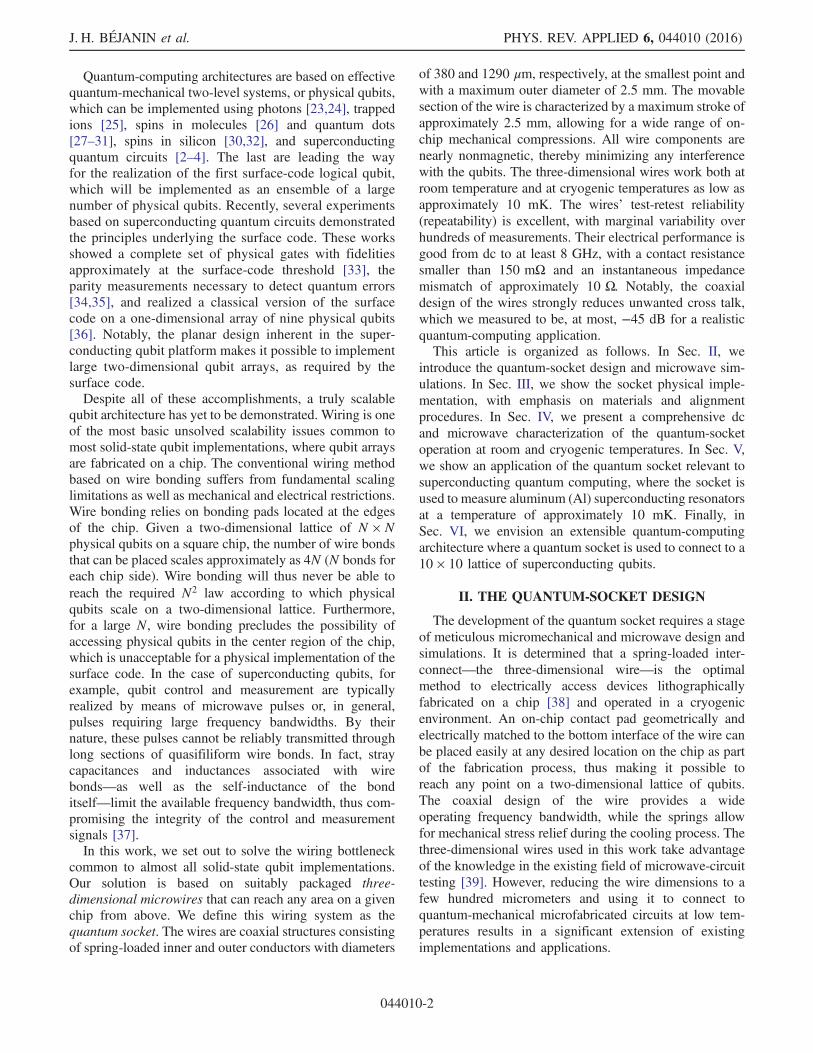
Cross talk is a phenomenon where a signal beingtransmitted through a channel generates an undesired signal
in a different channel. Interchannel isolation is the figure ofmerit that quantifies signal cross talk and that has to bemaximized to improve signal integrity. Cross talk can beparticularly large in systems operating at microwavefrequencies, where, if not properly designed, physicallyadjacent channels can be significantly affected by couplingcapacitances and/or inductances. In quantum-computingimplementations based on superconducting quantum cir-cuits, signal cross talk due to wire bonds has been identifiedto be an important source of errors, and methods to mitigateit have been developed [43,65,66]. However, cross talkremains an open challenge and isolations (the opposite ofcross talk) lower than 20 dB are routinely observed whenusing wire bonds [67]. The coaxial design of the three-dimensional wires represents an advantage over wirebonds. The latter, being open structures, radiate moreelectromagnetic energy that is transferred to adjacentcircuits. The former, being enclosed by the outer conductor,limit cross talk due to electromagnetic radiation.In realistic applications of the quantum socket, the
three-dimensional wires must land in close proximity toseveral on-chip transmission lines. In order to studyinterchannel isolation in such scenarios, we design aspecial device comprising a pair of CPW transmissionlines, as shown in the inset of Fig. 13(a). One trans-mission line connects two three-dimensional wires(ports 1 and 2), exactly as for the devices studied inSecs. IV B and IV C; the other line, which also connectstwo three-dimensional wires (ports 3 and 4), circumventsthe wire at port 1 by means of a CPW semicircle. Thedistance between the semicircle and the wire outerconductor is designed to be as short as possible,approximately 100 μm.The chip employed for the cross-talk tests is similar to
the Ag sample used for the quantum-socket microwavecharacterization and is part of a DUT analogous to thatshown in Fig. 8. The dc resistances of the center trace of the1-2 and 3-4 transmission lines are measured and found tobe approximately 2.8 and 4.5 Ω, respectively (note that the3-4 transmission line is approximately 18.0 mm long—hence the larger resistance). All dc resistances to the groundand between the two transmission lines are found to be onthe order of a few kilohms, demonstrating the absence ofundesired short-circuit paths. A four-port calibration and ameasurement of the DUT are conducted by means of aVNA (see Sec. S2 of the Supplemental Material for details[47]). Among the 16 S parameters, Fig. 13(a) shows themagnitude of the transmission coefficients S21 and S43,along with the magnitude of the cross-talk coefficients S31,S41, S32, and S42.The results show that the isolation in the typical qubit
operation bandwidth, between 4 and 8 GHz, is larger thanapproximately 45 dB. Note that the cross-talk coefficientsshown in Fig. 13(a) include attenuation, owing to the seriesresistance of the Ag transmission lines. The actual
(a)
(b)
FIG. 12. TDR measurement for the Ag sample at roomtemperature. (a) Measurement of port 1 of the setup in Fig. 8.(b) Enlargement of (a) addressing the three-dimensional wire andthe 90° transition region between the wire and the CPW trans-mission line (blue). The room-temperature Au data (red) are alsodisplayed as a reference.
J. H. BÉJANIN et al. PHYS. REV. APPLIED 6, 044010 (2016)
044010-16
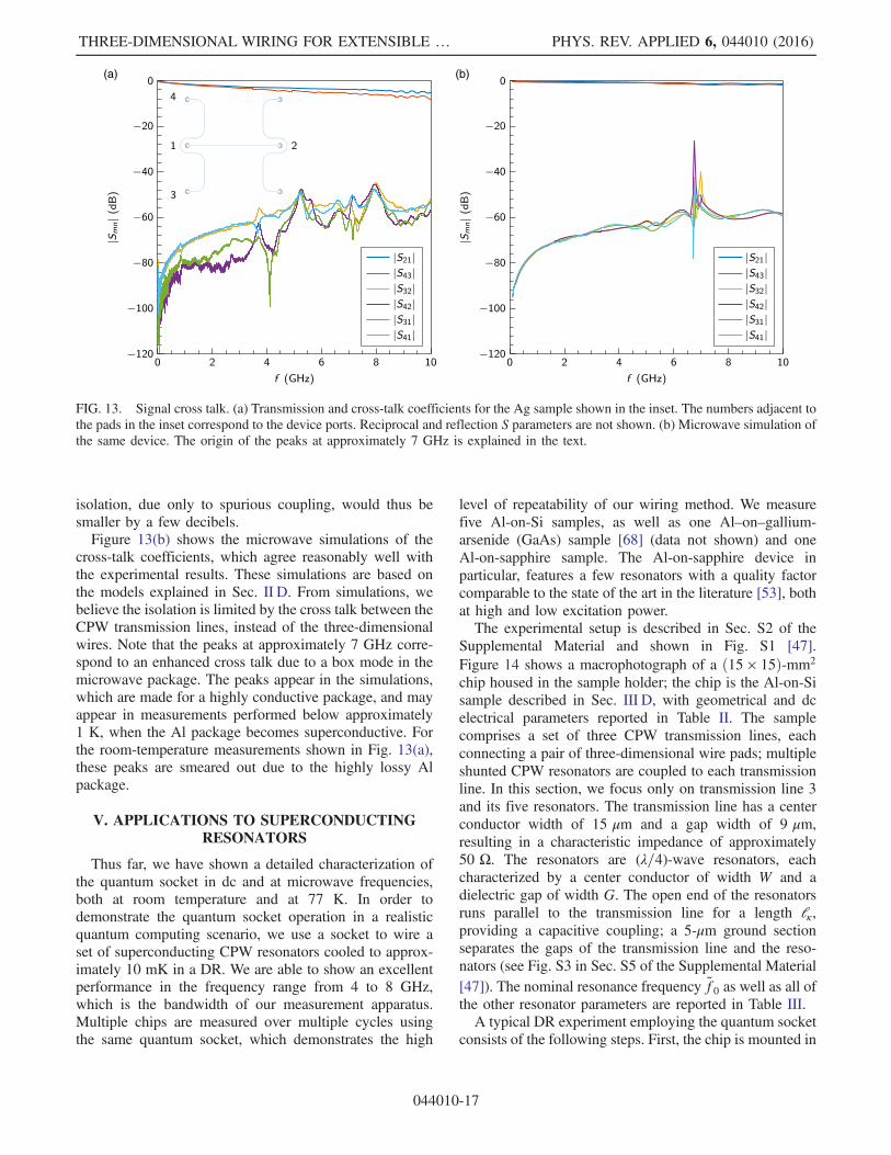
isolation, due only to spurious coupling, would thus besmaller by a few decibels.Figure 13(b) shows the microwave simulations of the
cross-talk coefficients, which agree reasonably well withthe experimental results. These simulations are based onthe models explained in Sec. II D. From simulations, webelieve the isolation is limited by the cross talk between theCPW transmission lines, instead of the three-dimensionalwires. Note that the peaks at approximately 7 GHz corre-spond to an enhanced cross talk due to a box mode in themicrowave package. The peaks appear in the simulations,which are made for a highly conductive package, and mayappear in measurements performed below approximately1 K, when the Al package becomes superconductive. Forthe room-temperature measurements shown in Fig. 13(a),these peaks are smeared out due to the highly lossy Alpackage.
V. APPLICATIONS TO SUPERCONDUCTINGRESONATORS
Thus far, we have shown a detailed characterization ofthe quantum socket in dc and at microwave frequencies,both at room temperature and at 77 K. In order todemonstrate the quantum socket operation in a realisticquantum computing scenario, we use a socket to wire aset of superconducting CPW resonators cooled to approx-imately 10 mK in a DR. We are able to show an excellentperformance in the frequency range from 4 to 8 GHz,which is the bandwidth of our measurement apparatus.Multiple chips are measured over multiple cycles usingthe same quantum socket, which demonstrates the high
level of repeatability of our wiring method. We measurefive Al-on-Si samples, as well as one Al–on–gallium-arsenide (GaAs) sample [68] (data not shown) and oneAl-on-sapphire sample. The Al-on-sapphire device inparticular, features a few resonators with a quality factorcomparable to the state of the art in the literature [53], bothat high and low excitation power.The experimental setup is described in Sec. S2 of the
Supplemental Material and shown in Fig. S1 [47].Figure 14 shows a macrophotograph of a ð15 × 15Þ-mm2
chip housed in the sample holder; the chip is the Al-on-Sisample described in Sec. III D, with geometrical and dcelectrical parameters reported in Table II. The samplecomprises a set of three CPW transmission lines, eachconnecting a pair of three-dimensional wire pads; multipleshunted CPW resonators are coupled to each transmissionline. In this section, we focus only on transmission line 3and its five resonators. The transmission line has a centerconductor width of 15 μm and a gap width of 9 μm,resulting in a characteristic impedance of approximately50 Ω. The resonators are (λ=4)-wave resonators, eachcharacterized by a center conductor of width W and adielectric gap of width G. The open end of the resonatorsruns parallel to the transmission line for a length lκ,providing a capacitive coupling; a 5-μm ground sectionseparates the gaps of the transmission line and the reso-nators (see Fig. S3 in Sec. S5 of the Supplemental Material[47]). The nominal resonance frequency ~f0 as well as all ofthe other resonator parameters are reported in Table III.A typical DR experiment employing the quantum socket
consists of the following steps. First, the chip is mounted in
(a) (b)
FIG. 13. Signal cross talk. (a) Transmission and cross-talk coefficients for the Ag sample shown in the inset. The numbers adjacent tothe pads in the inset correspond to the device ports. Reciprocal and reflection S parameters are not shown. (b) Microwave simulation ofthe same device. The origin of the peaks at approximately 7 GHz is explained in the text.
THREE-DIMENSIONAL WIRING FOR EXTENSIBLE … PHYS. REV. APPLIED 6, 044010 (2016)
044010-17

the microwave package, which has already been attached tothe package holder (see Secs. II C and III). Second, a seriesof dc tests is performed at room temperature. The results fora few Al-on-Si samples are reported in Table II. Third, thepackage-holder assembly is characterized at room temper-ature by measuring its S parameters. The results of such ameasurement are shown in Fig. 15(a). Fourth, the packageholder is mounted by means of the SMP connectors to theMC stage of the DR, and an S21 measurement is performed.The results (magnitude only) are shown in Fig. 15(b) in thefrequency range between 10 MHz and 10 GHz. Fifth, thevarious magnetic and radiation shields of the DR are closedand the DR is cooled down. Sixth, during cooldown, the S21measurement is repeated first at approximately 3 K, then atthe DR base temperature of approximately 10 mK. Theresults are shown in Figs. 15(b) and 15(c), respectively. Atapproximately 3 K, we note the appearance of a shallowdip at approximately 5.7 GHz, probably due to a screw-inmicroconnector becoming sightly loose during cooling (seeSec. IV B). It is important to mention that in the nextgeneration of three-dimensional wires we will eliminate the
screw-in microconnector since we believe we have found atechnique to overcome the soldering issues detailed inSec. II C (see Sec. VI for a brief description). At the basetemperature, all five resonators are clearly distinguishableas sharp dips on the relatively flat microwave backgroundof the measurement network. We then select a narrowerfrequency range around each resonator and make a finer S21measurement. For example, Fig. 15(d) shows the magni-tude and the phase of the resonance dip associated withresonator 2.The normalized inverse transmission coefficient ~S−121 is
fitted as in Ref. [53]. This procedure makes it possible toaccurately estimate both the internal Qi and the rescaledcouplingQ�
c quality factors of a resonator. The fit results areshown in Table III. The plot of the fits for the magnitudeand phase of S21 for resonator 2 are overlaid with themeasured data in Fig. 15(d). The real and imaginary partsof ~S−121 for the same resonator, as well as the associated fit,are shown in Fig. S4 in Sec. S5 of the SupplementalMaterial [47].The resonator mean photon number hnphi can be
estimated from the room-temperature power at the inputchannel Pin and the knowledge of the total input-channelattenuation α (see Sec. S2 of the Supplemental Material[47,69,70]). From basic circuit theory and Ref. [71], weobtain
hnphi ¼2
hπ2Q2
l
Q�c
P0in~f20
; ð4Þ
where h is the Planck constant, 1=Ql ¼ 1=Qi þ 1=Q�c is
the inverse loaded quality factor of the resonator, and P0in ¼
Pin=α is the power at the resonator input. For example,hnphi≃ 4.1 × 10⁷ for resonator 2.The fabrication process of the resonators described in
Table III is not optimized for high values of Qi, which,
TABLE III. Resonator parameters. The measured resonancefrequency is f0. The rescaled coupling and internal quality factorsQ�
c and Qi, respectively, are obtained from the fits of themeasured transmission coefficients (see the text for details).These quality factors are measured at a high resonator excitationpower, corresponding to hnphi > 105.
i~f0
ðMHzÞf0
ðMHzÞW
ðμmÞG
ðμmÞlκ
ðμmÞ Q�c Qi
1 4600.0 4673.2 8 5 400 5012 21 2432 5000.0 5064.5 15 9 300 16 002 165 7903 5800.0 5872.9 25 15 400 10 269 47 1654 7000.0 7091.7 15 9 300 6230 54 8945 7400.0 7520.1 8 5 400 4173 28 3536 4700.0 4717.6 15 9 45 244 960 1 977 551
FIG. 14. Macrophotograph of an Al chip on a Si substratemounted in a sample holder with a grounding washer. The imageshows three CPW transmission lines, each coupled to a set of(λ=4)-wave resonators. The grounding washer, with its fourprotruding feet, is placed above the chip covering the chip edges.The marks imprinted by the bottom interface of the three-dimensional wires on the Al pads are noticeable. More detailedimages of these marks are shown in Fig. 5. This chip and similarother chips with analogous microwave structures and geometries,including one Al-on-GaAs sample as well as one Al-on-sapphiresample, are used in the measurements at approximately 10 mK inthe DR.
J. H. BÉJANIN et al. PHYS. REV. APPLIED 6, 044010 (2016)
044010-18

however, is an important figure of merit for applications toquantum computing. In order to verify the compatibility ofthe quantum socket with resonators of higher quality, wedecide to fabricate a sample featuring an Al thin filmdeposited by means of a ultrahigh-vacuum electron-beamphysical vapor-deposition (EBPVD) system; the substrateof choice is, in this case, sapphire. The sample design issimilar to that shown in Fig. 14 and the sample preparationanalogous to that in Ref. [53]; fabrication details are inAppendix F. We are able to measure a few resonators with
Qi > 106 for large values of hnphi. For one of theseresonators, we measure Qi as a function of hnphi, as shownin Fig. 16. As expected from measurements in the literature[53], Qi decreases by approximately one order of magni-tude when the resonator mean photon number is reducedfrom hnphi≃ 106 to ≃10−2. For the lowest mean photonnumber, Qi ≃ 2.8 × 10⁵; such a quality factor is a goodindication that the quantum socket will likely preservequantum coherence sufficiently well when utilized for themanipulation of superconducting qubits.
(a) (b)
(c) (d)
FIG. 15. Measurements of Al-on-Si resonators. (a) Benchtop measurement of the S parameters of the CPW transmission line 3conducted at room temperature. (b) jS21j measurement of the same line with the chip mounted on the MC stage of the DR at roomtemperature (blue) and at approximately 3 K (red). (c) jS21j measurement of the sample at approximately 10 mK. The five dipscorrespond to (λ=4)-wave resonators. (d) Magnitude and phase of S21 for resonator 2.
THREE-DIMENSIONAL WIRING FOR EXTENSIBLE … PHYS. REV. APPLIED 6, 044010 (2016)
044010-19

VI. CONCLUSIONS
In a recent work [3], seven sequential stages necessary tothe development of a quantum computer were introduced.At that time, the next stage to be reached was theimplementation of a single logical qubit characterized byan error rate that was at least one order of magnitude lowerthan that of the underlying physical qubits. In order toachieve this task, a two-dimensional lattice of 10 × 10
physical qubits with an error rate of at most 10−3 wasrequired [22].Figure 17 shows an extensible quantum computing
architecture where a two-dimensional square lattice ofsuperconducting qubits is wired by means of a quantumsocket analogous to that introduced in this work. Thearchitecture comprises three main layers: the quantumhardware; the shielding interlayer; the three-dimensionalwiring mesh.As shown in Fig. 17(a), the quantum hardware is realized
as a two-dimensional lattice of superconducting qubits withnearest-neighbor interactions. The qubits are a modifiedversion of the Xmon presented in Ref. [59]. Each qubit ischaracterized by seven arms for coupling to one XY andone Z control line as well as one measurement resonatorand four interqubit-coupling resonators. We name this typeof qubit the heptaton. The interqubit coupling is mediatedby means of superconducting CPW resonators that allowthe implementation of control-Z (CZ) gates between two
neighboring qubits [72,73]. A set of four heptatons can beread out by way of a single CPW transmission lineconnected to four CPW resonators, each with a differentresonant frequency. Figure 17 also shows the on-chip padsassociated with each three-dimensional wire. In Sec. S7 ofthe Supplemental Material [47], we propose an extendedarchitecture where each qubit can be measured by means oftwo different resonators, one with a frequency above andthe other with a frequency below all of the coupling-resonator frequencies.Assuming a pitch between two adjacent three-
dimensional wires of 1 mm, the lateral dimension of onesquare cell having four heptatons at its edges is 8 mm. Thethree distances A, B, and C between the wire pads andthe resonators leading to this quantity are indicated inFig. 17(b). It is thus possible to construct a two-dimensional lattice of 10 × 10 heptatons on a squarechip with a lateral dimension 9 × 8 mm2 ¼ 72 mm2. Að72 × 72Þ-mm2 square chip is the largest chip that can bediced from a standard 4-in. wafer. This procedure will allowfor the implementation of a logical qubit based on thesurface code, with a distance of at least 5 [22]. In thisarchitecture, the coupling resonators act as a coherentspacer between pairs of qubits; i.e., they allow a sufficientseparation to accommodate the three-dimensional wires,while maintaining quantum coherence during the CZ gates.Additionally, these resonators will help mitigate qubit crosstalk compared to architectures based on direct capacitivecoupling between adjacent qubits (see Ref. [36]). In fact,they will suppress qubit-mediated coupling between neigh-boring control lines (a similar coupling mechanism to thatshown in Ref. [74]). It is worth noting that adjacentcoupling resonators can be suitably designed to be atdifferent frequencies, thus further diminishing qubit-mediated cross talk.Implementing a large qubit chip with a lateral dimension
of 72 mm presents significant challenges to the qubitoperation at microwave frequencies. A large chip mustbe housed in a large microwave package, causing theappearance of box modes that can interfere with the qubitcontrol and measurement sequences [43]. Moreover, alarge chip will inevitably lead to floating ground planesthat can generate unwanted slotline modes [43]. All of theseparasitic effects can be suppressed by means of theshielding interlayer, as shown in Fig. 17(a). This layercan be wafer bonded [5–8] to the quantum layer. Through-holes and cavities on the bottom part of the layer can bereadily fabricated using standard Si-etching techniques.The holes will house the three-dimensional wires, whereasthe cavities will accommodate the underlying qubit andresonator structures. Large substrates also generate chipmodes that, however, can be mitigated using buried metallayers and/or metalized through-silicon vias [65].The three-dimensional wires to be used for the
(10 × 10)-qubit architecture will be an upgraded version
FIG. 16. Measurement of Qi as a function of hnphi for one ofthe Al-on-sapphire resonators. The experimental settings used inthe measurements are reported in Sec. S2 of the SupplementalMaterial [47]; the confidence intervals are evaluated from thestandard errors of the fitting parameters of the normalized inversetransmission coefficient ~S−121 and are smaller than the diamondsymbols. All measurements are performed at approximately10 mK. The typical-quality-factor “S curve” is observed; theplateaus on the leftmost and rightmost regions of the curveindicate the reaching of low values of hnphi and saturation of thetwo-level systems, respectively [53].
J. H. BÉJANIN et al. PHYS. REV. APPLIED 6, 044010 (2016)
044010-20

of the wires used in this work. In particular, the M2.5 threadwill be removed and the wires will be inserted in adedicated substrate [see Fig. 17(a)]; additionally, thescrew-in microconnector will be substituted by a directconnection to a subminiature push-on submicroconnector(SMPS) (not shown in the figure).In future applications of the quantum socket, we envision
an architecture where the three-dimensional wires will beused as an interconnect between the quantum layer and aclassical control or measurement layer. The classical layercould be realized using rapid single-flux quantum (RSFQ)digital circuitry [75,76]. For example, high-sensitivitydigital down-converters (DDCs) have been fabricatedbased on RSFQ electronics [77]. Such circuitry is operatedat very low temperatures and can substitute for the room-temperature electronics used for qubit readout. Note thatcryogenic DDC chips with dimensions of less than 5 ×5 mm2 can perform the same operations presently carriedout by room-temperature microwave equipment with anoverall footprint of approximately 50 × 50 cm2. Recentinterest in reducing dissipation in RSFQ electronics [78]
will possibly enable the operation of the classical elec-tronics in close proximity to the quantum hardware. Wealso believe it is feasible to further miniaturize the three-dimensional wires so that the wire’s outer diameter wouldbe on the order of 500 μm. Assuming a wire-wire pitch alsoof 500 μm, it will therefore be possible to realize a lattice of250 000 wires connecting to approximately 105 qubitsarranged on a 315 × 315 two-dimensional qubit grid withdimensions of 1 × 1m2. This lattice will allow for theimplementation of simple fault-tolerant operations betweena few tens of logical qubits [22].
ACKNOWLEDGMENTS
Matteo Mariantoni and the Digital Quantum MatterLaboratory acknowledge the Alfred P. Sloan Foundationas well as the Natural Sciences and Engineering ResearchCouncil of Canada (NSERC), the Ministry of Researchand Innovation (MRI) of Ontario, and the CanadianMicroelectronics Corporation (CMC) Microsystems.C. R. H.M. acknowledges support from a Waterloo
(a) (b)
FIG. 17. Extensible quantum-computing architecture. (a) The three main layers of the architecture: the quantum hardware (bottomlayer), the shielding interlayer (middle layer), and the three-dimensional wiring mesh (top layer), with wires indicated in yellow. Thevertical dashed lines with double arrows show the mounting procedure to be used to prepare the assembly. The (thinner) middle layerwill be metalized on the bottom and wafer bonded to the quantum layer beneath; both the through-holes that accommodate the three-dimensional wires and the tunnels above the qubits and manipulation lines are shown. The back end of the wires (top layer) will beconnected to SMPS connectors (not shown). (b) Two-dimensional view of the quantum hardware. The substrate is indicated in darkblue, the heptatons in light blue, the coupling resonators in magenta, the four readout resonators in red, green, orange, and cyan, and,finally, the wire pads and associated lines in yellow. The distances between the coupling resonators and the wire pads are A ¼ C ¼2.25 mm and B ¼ 3.5 mm. Note that the Z control lines are represented as galvanically connected to the heptatons, in a fashion similarto Ref. [59]. The measurement can be multiplexed so that four qubits are read out by one line only.
THREE-DIMENSIONAL WIRING FOR EXTENSIBLE … PHYS. REV. APPLIED 6, 044010 (2016)
044010-21

Institute for Nanotechnology (WIN) Nanofellowship–2013 and J. H. B. a Provost’s Entrance Award of theUniversity of Waterloo (UW). We acknowledge ourfruitful discussions with John M. Martinis and theMartinis Group, Eric Bogatin, and William D. Oliver.We thank the group of Adrian Lupascu as well as PatrickSmutek of Plassys-Bestek SAS for their assistance in thedeposition of Al films and Nathan Nelson-Fitzpatrick andthe UW’s Quantum NanoFab Facility for their supportwith device fabrication. We thank Dario Mariantoni andAlexandra V. Bardysheva for their help with a fewimages and figures.J. H. B. and T. G. M. contributed equally to this work.
APPENDIX A: WIRE COMPRESSION
In this appendix, we discuss the pressure settings of thethree-dimensional wires. In the current implementation ofthe quantum socket, the pressure exerted by the three-dimensional wires on the chip is controlled by the instal-lation depth of the wire in the lid. This depth depends on thenumber of rotations used to screw the wire into the M2.5-threaded hole of the lid. Since the wire’s tunnel has to bealigned with the corresponding on-chip pad, a discretenumber of wire pressure settings is allowed. For thepackage shown in Figs. 1(b) and 4(b), the minimum lengthan unloaded wire has to protrude from the ceiling of thelid’s internal cavity to touch the top surface of the chip islc ¼ 3.05 mm [see Fig. 1(c)]. For a maximum wire strokeΔL ¼ 2.5 mm, the maximum length an unloaded wire canprotrude from the cavity ceiling without breaking whenloaded is lc þ ΔL ¼ 5.55 mm. The first allowed pressuresetting, with wire and pad perfectly aligned, is forlp ¼ 3.10 mm. The pitch for an M2.5 screw is0.45 mm. Hence, five pressure settings are nominallypossible, for lp ¼ 3.10þ 0.45k mm, with k ¼ 1; 2;…; 5.We find the ideal pressure setting to be when k ¼ 3,corresponding to a nominal lp ¼ 4.45 mm; the actualaverage setting for 12 wires is measured to belp ¼ 4.48 ∓ 0.28 mm, with standard deviation due tothe machining tolerances. For greater depths, we experi-ence occasional wire damage; lesser depths are not inves-tigated. Possible effects on the electrical properties of thethree-dimensional wires due to different pressure settingswill be studied in a future work.
APPENDIX B: MAGNETISM
In this appendix, we describe the measurement setupemployed to characterize the magnetic properties of thematerials used in the quantum socket and present the mainmeasurement results. Additionally, we give an estimate ofthe strength of the magnetic field caused by one three-dimensional wire inside the microwave package.The ZGC used in our tests comprises three nested
cylinders, each with a lid with a central circular hole;the hole in the outermost lid is extended into a chimney thatprovides further magnetic shielding. The walls of the ZGCare made of an alloy of Ni and Fe (or a mu-metal alloy)with a high relative magnetic permeability μr. The alloyused for the chamber is a Co-Netic® AA alloy and ischaracterized by a dc-relative magnetic permeability at40 G, μ40dc ¼ 80 000, and an ac-relative magnetic permeabil-ity at 60 Hz and at 40 G, μ40ac ¼ 65 000. As a consequence,the nominal magnetic-field attenuation lies between 1000and 1500. The ZGC used in our tests is manufactured bythe Magnetic Shield Corporation (model ZG-209).The flux-gate magnetometer used to measure the mag-
netic field ~B is a three-axis dc milligauss meter fromAlphaLab, Inc. (model MGM3AXIS). Its sensor is a ð38 ×25 × 25Þ-mm3 parallelepiped at the end of an approxi-mately 1.2-m-long cable; the orientation of the sensor iscalibrated to within 0.1° and has a resolution of 0.01 mG(i.e., 1 nT) over a range of ∓2000 mG (i.e., ∓200 μT).The actual attenuation of the chamber is tested by
measuring the value of Earth’s magnetic field with andwithout the chamber in two positions, vertical and hori-zontal; inside the chamber, the measurements are per-formed a few centimeters from the chamber’s base,approximately on the axis of the inner cylinder. In theseand all subsequent tests, the magnetic sensor is kept in thesame orientation and position. The results are reported inTable V, which shows the type of measurement performed,the magnitude of the measured magnetic field ∥~B∥, and theattenuation ratio α. The maximum measured attenuation isα≃ 917 in the horizontal position.The ZGC characterization of Table V also serves as a
calibration for the measurements on the materials usedfor the quantum socket. In these measurements, each testsample is positioned approximately 1 cm away from themagnetic sensor. The results, which are reported in
TABLE IV. Chemical composition (wt %) of the two main materials used in the three-dimensional wires. Copper, Cu; tin, Sn; zinc, Zn;lead, Pb; phosphorus, P.
Material Cu Sn Zn Fe Ni Pb P Si Others
CW724Ra 73–77 0.3 rest 0.3 0.2 ≤ 0.09 0.04–0.10 2.7–3.4 Al ¼ 0.05, manganese ¼ 0.05CW453Kb rest 7.5–8.5 ≤ 0.2 ≤ 0.1 ≤ 0.2 ≤ 0.02 0.01–0.4 � � � 0.2
aSee Ref. [80].bSee Ref. [81].
J. H. BÉJANIN et al. PHYS. REV. APPLIED 6, 044010 (2016)
044010-22

Table VI, are obtained by taking the magnitude of thecalibrated field of each sample. The calibrated field itself iscalculated by subtracting the background field from thesample field, component by component. Note that thebackground and sample fields are on the same order ofmagnitude (between 0.10 and 0.80 mG), with backgroundfluctuations on the order of 0.10 mG. Thus, we record themaximum value of each x, y, and z component.Considering that the volume of the measured samples issignificantly larger than that of the actual quantum-socketcomponents, we are confident that the measured magneticfields of the materials should be small enough not tosignificantly disturb the operation of superconductingquantum devices. As part of our magnetism tests, wemeasure a block of approximately 200 g of 5N5 Al inthe ZGC; as shown in Table VI, the magnitude of themagnetic field is found to be within the noise floor of themeasurement apparatus [79].A simple geometric argument allows us to estimate the
actual magnetic field due to one three-dimensional wire,without taking into account effects due to superconductiv-ity (most of the wire is embedded in an Al package, whichis superconductive at the qubit operation temperatures). Weassume that one wire generates a magnetic field of 0.25 mG(i.e., the maximum field value in Table VI; this overesti-mate is large, considering that the tested samples havevolumes much larger than any component in the wires) andis a magnetic dipole positioned 15 mm away from a qubit.The field generated by the wire at the qubit will then beBq ≃ 0.25r30=0.015
3 mG, where r0 ≃ 10 mm is the dis-tance at which the field is measured in the ZGC; thus,Bq ≃ 0.075 mG. Assuming an Xmon qubit with a
superconducting quantum interference device (SQUID)of dimensions 40 × 10 μm2 (cf. Ref. [59]), the estimatedmagnetic flux due to the wire threading the SQUID isΦq ≃ 4 × 10⁻¹⁸ Wb. This estimate is approximately 3orders of magnitude smaller than a flux quantumΦ0 ≃ 2.07 × 10⁻¹⁵ Wb; typical flux values for the Xmonoperation are on the order of 0.5Φ0.
APPENDIX C: THERMAL CONDUCTANCEOF A THREE-DIMENSIONAL WIRE
In this appendix, we describe the method used toestimate the thermal performance of a three-dimensionalwire and compare it to that of an Al-wire bond. Note that atvery low temperatures, thermal conductivities can vary byorders of magnitude between two different alloys of thesame material. The following estimate can thus only beconsidered correct to within approximately one order ofmagnitude. Thermal conductivity is a property intrinsic to amaterial. To characterize the cooling performance of athree-dimensional wire, we instead use the heat-transferrate (power) per kelvin difference, which depends on theconductivity.The power transferred across an object with its two
extremities at different temperatures depends on the cross-sectional area of the object, its length, and the temperaturedifference between the extremities. Since the cross sectionof a three-dimensional wire is not uniform, we assume thatthe wire is made of two concentric hollow cylinders. Thecross-sectional area of the two cylinders is calculated byusing dimensions consistent with those of a three-dimensional wire. The inner and outer hollow cylindersare assumed to be made of phosphor bronze and brassalloys, respectively. The thermal conductivities of thesematerials at low temperatures are determined by extrapo-lating measured data to 25 mK [82].The Al-wire bonds are assumed to be solid cylinders
with a diameter of 50 μm. In the superconducting state, thethermal conductivity of Al can be estimated by extrapo-lating from values in the literature [83].The heat-transfer rate per kelvin difference is calculated
by multiplying the thermal conductivity kt with the cross-sectional area A and dividing it by the length of the thermalconductor l. The heat-transfer rate per kelvin difference ofa three-dimensional wire is calculated by summing theheat-transfer rate per kelvin difference of the inner con-ductor to that of the outer conductor, and it is found to beΠt ≃ 6 × 10⁻⁷ WK−1 at 25 mK. At the same temperature,the heat-transfer rate per kelvin difference of a typicalAl-wire bond is estimated to beΠb ≃ 4 × 10⁻¹² WK−1 (seeTable VII), much lower than for a single three-dimensionalwire. Note that, instead of Al-wire bonds, gold-wire bondscan be used. These bonds are characterized by a higherthermal conductivity because they remain normal conduc-tive also at very low temperatures. However, Al-wire bonds
TABLE V. ZGC calibration. The margins of error indicated inparentheses are estimated from the fluctuation of the magneticsensor.
Measurement ∥~B∥ (mG) α
Vertical position, background field 554(20) � � �Vertical position, with ZGC 0.66(5) 842(34)Horizontal position, background field 539(20) � � �Horizontal position, with ZGC 0.59(5) 917(44)
TABLE VI. Magnetic-field measurements of the materials usedfor the main components of the quantum socket. The testedsamples are significantly larger than any component used in theactual implementation of the three-dimensional wires and micro-wave package. The margins of error indicated in parentheses areestimated from the fluctuation of the magnetic sensor.
Material ∥~B∥ (mG)
CW724R 0.21(5)CW453K 0.25(5)Al 5N5 0.02(5)
THREE-DIMENSIONAL WIRING FOR EXTENSIBLE … PHYS. REV. APPLIED 6, 044010 (2016)
044010-23
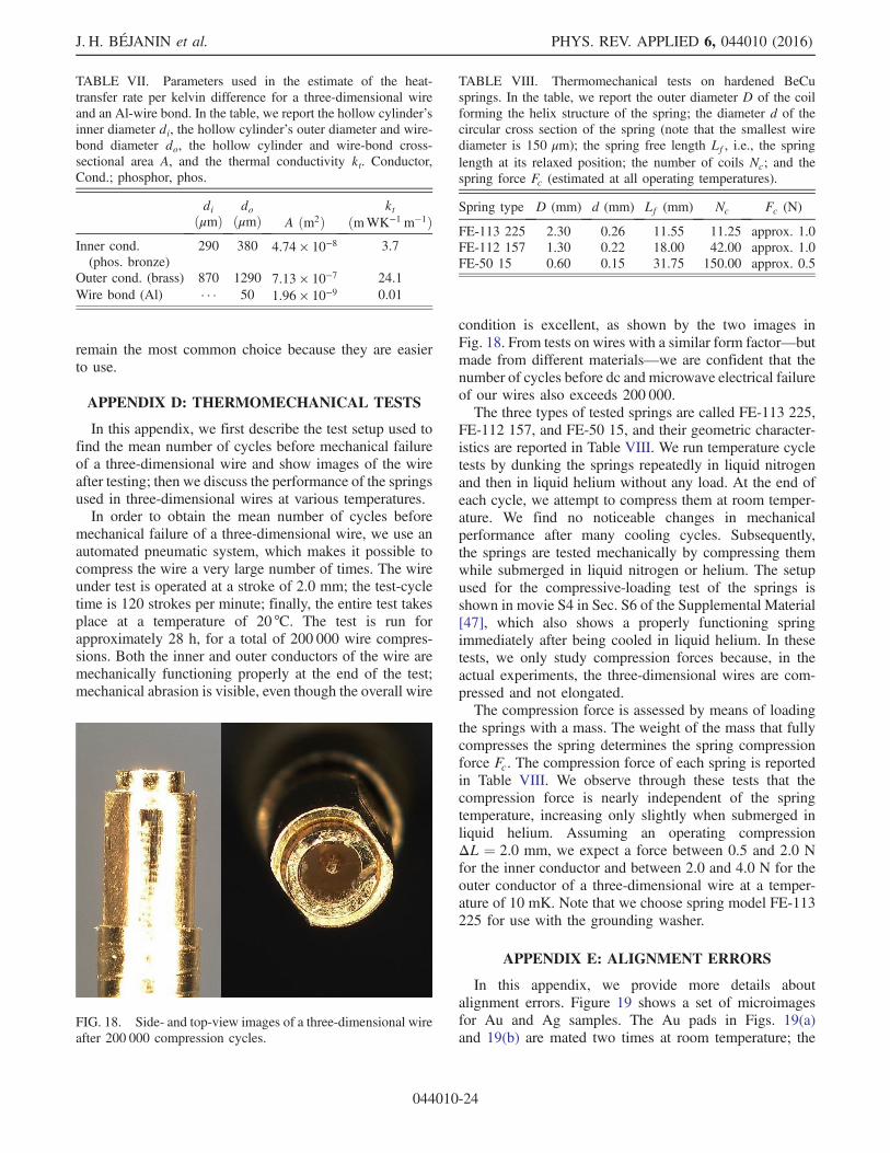
remain the most common choice because they are easierto use.
APPENDIX D: THERMOMECHANICAL TESTS
In this appendix, we first describe the test setup used tofind the mean number of cycles before mechanical failureof a three-dimensional wire and show images of the wireafter testing; then we discuss the performance of the springsused in three-dimensional wires at various temperatures.In order to obtain the mean number of cycles before
mechanical failure of a three-dimensional wire, we use anautomated pneumatic system, which makes it possible tocompress the wire a very large number of times. The wireunder test is operated at a stroke of 2.0 mm; the test-cycletime is 120 strokes per minute; finally, the entire test takesplace at a temperature of 20 °C. The test is run forapproximately 28 h, for a total of 200 000 wire compres-sions. Both the inner and outer conductors of the wire aremechanically functioning properly at the end of the test;mechanical abrasion is visible, even though the overall wire
condition is excellent, as shown by the two images inFig. 18. From tests on wires with a similar form factor—butmade from different materials—we are confident that thenumber of cycles before dc and microwave electrical failureof our wires also exceeds 200 000.The three types of tested springs are called FE-113 225,
FE-112 157, and FE-50 15, and their geometric character-istics are reported in Table VIII. We run temperature cycletests by dunking the springs repeatedly in liquid nitrogenand then in liquid helium without any load. At the end ofeach cycle, we attempt to compress them at room temper-ature. We find no noticeable changes in mechanicalperformance after many cooling cycles. Subsequently,the springs are tested mechanically by compressing themwhile submerged in liquid nitrogen or helium. The setupused for the compressive-loading test of the springs isshown in movie S4 in Sec. S6 of the Supplemental Material[47], which also shows a properly functioning springimmediately after being cooled in liquid helium. In thesetests, we only study compression forces because, in theactual experiments, the three-dimensional wires are com-pressed and not elongated.The compression force is assessed by means of loading
the springs with a mass. The weight of the mass that fullycompresses the spring determines the spring compressionforce Fc. The compression force of each spring is reportedin Table VIII. We observe through these tests that thecompression force is nearly independent of the springtemperature, increasing only slightly when submerged inliquid helium. Assuming an operating compressionΔL ¼ 2.0 mm, we expect a force between 0.5 and 2.0 Nfor the inner conductor and between 2.0 and 4.0 N for theouter conductor of a three-dimensional wire at a temper-ature of 10 mK. Note that we choose spring model FE-113225 for use with the grounding washer.
APPENDIX E: ALIGNMENT ERRORS
In this appendix, we provide more details aboutalignment errors. Figure 19 shows a set of microimagesfor Au and Ag samples. The Au pads in Figs. 19(a)and 19(b) are mated two times at room temperature; the
TABLE VII. Parameters used in the estimate of the heat-transfer rate per kelvin difference for a three-dimensional wireand an Al-wire bond. In the table, we report the hollow cylinder’sinner diameter di, the hollow cylinder’s outer diameter and wire-bond diameter do, the hollow cylinder and wire-bond cross-sectional area A, and the thermal conductivity kt. Conductor,Cond.; phosphor, phos.
diðμmÞ
doðμmÞ A ðm2Þ
ktðmWK−1 m−1Þ
Inner cond.(phos. bronze)
290 380 4.74 × 10⁻⁸ 3.7
Outer cond. (brass) 870 1290 7.13 × 10⁻⁷ 24.1Wire bond (Al) � � � 50 1.96 × 10⁻⁹ 0.01
FIG. 18. Side- and top-view images of a three-dimensional wireafter 200 000 compression cycles.
TABLE VIII. Thermomechanical tests on hardened BeCusprings. In the table, we report the outer diameter D of the coilforming the helix structure of the spring; the diameter d of thecircular cross section of the spring (note that the smallest wirediameter is 150 μm); the spring free length Lf, i.e., the springlength at its relaxed position; the number of coils Nc; and thespring force Fc (estimated at all operating temperatures).
Spring type D (mm) d (mm) Lf (mm) Nc Fc (N)
FE-113 225 2.30 0.26 11.55 11.25 approx. 1.0FE-112 157 1.30 0.22 18.00 42.00 approx. 1.0FE-50 15 0.60 0.15 31.75 150.00 approx. 0.5
J. H. BÉJANIN et al. PHYS. REV. APPLIED 6, 044010 (2016)
044010-24

three-dimensional wires used to mate these pads feature thesmaller tunnel (500 μm width). The pad dimensions areWp ¼ 230 μm and Tp ¼ 1000 μm. Noticeably, for the padin Fig. 19(a), the wire bottom interface matches the contactpad in both mating instances, even though the matching isaffected by a rotational misalignment of approximately 15°with respect to the transmission-line longitudinal axis.However, for the pad in Fig. 19(b), the lateral misalignmentis significant enough that the inner conductor lands on thedielectric gap in the second mating instance.In our initial design, a perfect match required that the die
dimensions should be, at most, 1 thou smaller than thedimensions of the chip recess, as machined. In the case ofthe sample holder used to house the Au samples, thechip-recess side lengths are 15.028(5), 15.030(5), 15.013(5), and 15.026(5) mm. The Au samples are diced from a Siwafer using a dicing saw from DISCO (model DAD-2H/6),
set to obtain a ð15 × 15Þ-mm2 die. Owing to the sawinaccuracies, the actual die dimensions are14.96ð1Þ × 14.96ð1Þ mm2, significantly smaller than thechip-recess dimensions. This size difference causes the dieto shift randomly between different mating instances,generating significant alignment errors.As described in the text, in order to minimize such errors,
a superior DISCO saw is used, in combination with aDISCO electroformed bond-hub diamond-blade modelZH05-SD 2000-N1-50-F E; this blade corresponds to anominal kerf between 35 and 40 μm. Additionally, we userotational as well as lateral aligning markers; the latter arespaced with increments of 10 μm that allow us to cut dieswith dimensions ranging from 14.97 to 15.03 mm, wellwithin the machining tolerances of the sample holder. Aftermachining, the actual inner dimensions of each sampleholder are measured by means of a measuring microscope.The wafers are then cut by selecting the lateral dicingmarkers associated with the die dimensions that best fit theholder being used.Figure 19(c) shows a successful alignment for six Ag
pads on the same chip; the chip is mounted in a sampleholder with a grounding washer. All three main steps for anideal and repeatable alignment (see Sec. III D) are fol-lowed. Figure 19(d) shows the distinctive marks left by thegrounding washer on an Ag film. The marks are localizedtowards the edge of the die; the washer covers approx-imately a width of 500 μm of Ag film. Such a width resultsin a good electrical contact at the washer-film interface.In conclusion, it is worth commenting upon some of the
features in Fig. 5(d). The figure clearly shows the draggingof a three-dimensional wire due to cooling contractions.In fact, for the Al chip recess, an estimate of the lateralcontraction length from room temperature to approximately4 K can be obtained as ΔLAl ¼ αð4ÞLAl ≃ ð4.15 × 10⁻³Þð15 × 10−3mÞ≃ 62 μm, where αð4Þ is the integrated linearthermal-expansion coefficient for Al 6061-T6 [84] at 4 Kfrom Ref. [61] and LAl is the room-temperature length ofthe recess side [85]. Note that the sample holder is actuallymade from Al alloy 5N5; however, different Al alloyscontract by approximately the same quantity. For the Sisample substrate, the lateral contraction length from roomtemperature to about 4 K is approximately given byΔLSi ≃ 3.2 μm, where the integrated linear thermal-expan-sion coefficient at 4 K is found in Table 2 of Ref. [86].Below 4 K, the thermal expansion of both materials isnegligible for our purposes, and thus the 4-K estimate canalso be considered valid at approximately 10 mK.
APPENDIX F: SAMPLE FABRICATION
In this appendix, we outline the fabrication processes forthe samples used to test the quantum socket. A set ofsamples is made by lift-off of a 3-μm Ag film, which isgrown by means of EBPVD (a system from IntlvacCanada Inc., model Nanochrome II) on a 3-in. float-zone
(b) (d)
(a) (c)
FIG. 19. Microimages showing three-dimensional wire align-ment errors. (a),(b) Au pads. The pad displayed in (a) isconnected to that in (b) by way of a CPW transmission lineapproximately 11.5 mm long. The die shifted upward betweenthe first (arrow 1) and second (arrow 2) mating instance, resultingin a lateral misalignment for the bottom pad. The rotationalmisalignment for the pad in (a) is indicated by a dashed line.(c) Successful alignment for six Ag pads on the same chip.(d) Peripheral area of an Ag sample (ground plane). The marksare attributed to contact with the grounding washer.
THREE-DIMENSIONAL WIRING FOR EXTENSIBLE … PHYS. REV. APPLIED 6, 044010 (2016)
044010-25

(FZ) Si (100) wafer with a thickness of 500 μm. Thesuperconducting Al-on-Si samples are made by etching a120-nm Al film that is deposited by EBPVD on a 500-μmFZ Si wafer. The Al-on-sapphire sample is made by etchinga 100-nm Al film that is deposited by an UHV EBPVD (asystem from Plassys-Bestek SAS) on a 500-μm c-planesingle-crystal sapphire wafer. Prior to deposition, the waferis annealed in vacuo at approximately 850 °C, while beingcleaned by way of molecular oxygen; a 1-nm germaniumbuffer layer is grown at room temperature before we depositthe Al film. Last, two sets of test samples are made byetching Au films with thicknesses of 100 and 200 nm, witha 10-nm Ti adhesion underlayer in both sets. The films aregrown by EBPVD (Intlvac) on a 3-in. Czochralski undopedSi (100) wafer with a thickness of 500 μm.The 3-μm Ag samples are required to reduce the series
resistance of the CPW transmission lines (see Secs. IV B,IV C, and IV D). Fabricating such a relatively thick filmnecessitates a more complex process than that used for theAu and Al samples. The Ag samples are fabricated with athick resist tone-reversal process. The wafer is spun with anAZ P4620 positive tone resist to create a resist thickness ofapproximately 14 μm, then soft baked for 4 min at 110 °C.Because the resist layer is so thick, a rehydration step of30 min is necessary before exposure. Optical exposure isperformed for 30 s in a mask aligner from SÜSS MicroTecAG (model MA6), in soft contact with a photomask. Afterexposure, the sample is left resting for at least 3 h so thatany nitrogen created by the exposure can dissipate. The
tone-reversal bake is done for 45 min in an oven set to90 °C, filled with ammonia gas. The sample then undergoesa flood exposure for 60 s and is developed in AZ® 400 Kfor 15 min. Subsequently, 3 μm of Ag is deposited andlift-off of the resist is performed in acetone for 5 min withultrasound.
APPENDIX G: MICROWAVE PARAMETERS
In this appendix, we present a set of microwaveparameters that help further analyze the performance ofthe quantum socket. These parameters are obtained fromthe measured S-parameter data of Figs. 9 and 10(a) and areshown in Fig. 20. The complex input impedance can beobtained from the frequency-dependent impedance matrixZ ¼ ½Zmn� as [87]
Zin ¼ Z11 −Z12Z21
Z22 − ZL; ðG1Þ
where ZL ¼ Zc ¼ 50 Ω is the load impedance. Theimpedance matrix is obtained using the measured complexS-parameter matrix S ¼ ½Smn� from
Z ¼ffiffiffiffiffi
Zc
p
��
1 0
0 1
�
þ S
���
1 0
0 1
�
− S
�−1ffiffiffiffiffi
Zc
p
: ðG2Þ
The magnitude of Zin is shown in Fig. 20(a).
(a)
(b)
(c)
(d)
FIG. 20. Quantum-socket microwave parameters. (a) Input impedance magnitude jZinj. (b) Input VSWR, VSWRin. (c) Phase delay τϕ.(d) Group delay τg. Blue corresponds to the Au sample at room temperature (RT), red to the Au sample at 77 K, and orange to the Agsample at RT.
J. H. BÉJANIN et al. PHYS. REV. APPLIED 6, 044010 (2016)
044010-26

The input voltage standing-wave ratio (VSWR) isobtained from [41]
VSWRin ¼1þ jS11j1 − jS11j
ðG3Þ
and is displayed in Fig. 20(b).The phase delay is calculated as [87]
τϕ ¼ −1
2π
∠S21f
ðG4Þ
and is displayed in Fig. 20(c).Finally, the group delay is obtained from [41]
τg ¼ −1
2π
∂∂f ð∠S21Þ ðG5Þ
and is displayed in Fig. 20(d). The derivative in Eq. (G5) isevaluated numerically by means of central finite differenceswith sixth-order accuracy. The data in Fig. 20(d) arepostprocessed using 1% smoothing. Note that the outputimpedance and the VSWR are also evaluated and resemblethe corresponding input parameters.The input and output impedances as well as the VSWRs
indicate a good impedance matching up to approximately8 GHz. The phase and group delays, which are directlyrelated to the frequency dispersion associated with thequantum socket, indicate minimal dispersion. This result isexpected for a combination of coaxial structures (the three-dimensional wires) and a CPW transmission line. Thus, weexpect wideband control pulses to be transmitted withoutsignificant distortion in applications with superconductingqubits (see Sec. S8 of the Supplemental Material [47] forfurther details on microwave-pulse transmission).
[1] D. Deutsch, Quantum theory, the Church-Turing principleand the universal quantum computer, Proc. R. Soc. A 400,97 (1985).
[2] John Clarke and Frank K. Wilhelm, Superconductingquantum bits, Nature (London) 453, 1031 (2008).
[3] Michel H. Devoret and Robert J. Schoelkopf, Supercon-ducting circuits for quantum information: An outlook,Science 339, 1169 (2013).
[4] John M. Martinis, Qubit metrology for building a fault-tolerant quantum computer, NPJ Quantum Inf. 1, 15005(2015).
[5] Timothy M. Miller, Christine A. Jhabvala, Edward Leong,Nicholas P. Costen, Elmer Sharp, Tomoko Adachi, andDominic J. Benford, in High Energy, Optical, and InfraredDetectors for Astronomy V, edited by Andrew D. Hollandand James W. Beletic, SPIE Proceedings Vol. 8453 (SPIE-International Society for Optical Engineering, Bellingham,WA, 2012), p. 84532H.
[6] David W. Abraham, Jerry M. Chow, Antonio D. CórcolesGonzalez, George A. Keefe, Mary E. Rothwell, JamesR. Rozen, and Matthias Steffen, Removal of spuriousmicrowave modes via flip-chip crossover, U.S. PatentNo. 13/838,324 (22 December 2015).
[7] Teresa Brecht, Matthew Reagor, Yiwen Chu, WolfgangPfaff, Chen Wang, Luigi Frunzio, Michel H. Devoret, andRobert J. Schoelkopf, Demonstration of superconductingmicromachined cavities, Appl. Phys. Lett. 107, 192603(2015).
[8] Danna Rosenberg, Donna-Ruth Yost, Rabindra Das, DavidHover, Livia Racz, Steven Weber, Jonilyn Yoder, AndrewKerman, and William Oliver, in Proceedings of the APSMarch Meeting, 2016.
[9] Pedram Roushan et al., Chiral groundstate currents ofinteracting photons in a synthetic magnetic field, arXiv:1606.00077.
[10] Alessandro Bruno, Stefano Poletto, Nadia Haider, andLeonardo DiCarlo, in Proceedings of the APS MarchMeeting, 2016.
[11] Jay M. Gambetta, Jerry M. Chow, and Matthias Steffen,Building logical qubits in a superconducting quantumcomputing system, arXiv:1510.04375.
[12] Teresa Brecht, Wolfgang Pfaff, Chen Wang, YiwenChu, Luigi Frunzio, Michel H. Devoret, and Robert J.Schoelkopf, Multilayer microwave integrated quantum cir-cuits for scalable quantum computing, NPJ Quantum Inf. 2,16002 (2016).
[13] David P. DiVincenzo, Quantum computation, Science 270,255 (1995).
[14] Michael A. Nielsen and Isaac L. Chuang, Quantum Com-putation and Quantum Information (Cambridge UniversityPress, Cambridge, England, 2000).
[15] David P. DiVincenzo, The physical implementation ofquantum computation, Fortschr. Phys. 48, 771 (2000).
[16] N. David Mermin, Quantum Computer Science: An Intro-duction (Cambridge University Press, Cambridge, England,2007).
[17] Thaddeus D. Ladd, Fedor Jelezko, Raymond Laflamme,Yasunobu Nakamura, Christopher Monroe, and Jeremy L.O’Brien, Quantum computers, Nature (London) 464, 45(2010).
[18] Carlos A. Pérez-Delgado and Pieter Kok, Quantum com-puters: Definition and implementations, Phys. Rev. A 83,012303 (2011).
[19] Ashley Montanaro, Quantum algorithms: An overview,NPJ Quantum Inf. 2, 15023 (2016).
[20] Daniel Gottesman, An introduction to quantum error cor-rection and fault-tolerant quantum computation, Proc.Symp. Appl. Math. 68, 13 (2010).
[21] Robert Raussendorf and Jim Harrington, Fault-TolerantQuantum Computation with High Threshold in TwoDimensions, Phys. Rev. Lett. 98, 190504 (2007).
[22] Austin G. Fowler, Matteo Mariantoni, John M. Martinis,and Andrew N. Cleland, Surface codes: Towards practicallarge-scale quantum computation, Phys. Rev. A 86, 032324(2012).
[23] Pieter Kok, William J. Munro, Kae Nemoto, Timothy C.Ralph, Jonathan P. Dowling, and Gerard J. Milburn, Linearoptical quantum computing with photonic qubits, Rev. Mod.Phys. 79, 135 (2007).
THREE-DIMENSIONAL WIRING FOR EXTENSIBLE … PHYS. REV. APPLIED 6, 044010 (2016)
044010-27

[24] Jeremy L. O’Brien, Akira Furusawa, and Jelena Vućković,Photonic quantum technologies, Nat. Photonics 3, 687(2009).
[25] Christopher Monroe and Jungsang Kim, Scaling the ion trapquantum processor, Science 339, 1164 (2013).
[26] David Cory, in Frontiers in Optics, OSA Technical Digest(CD) (Optical Society of America, Washington, DC, 2006),p. LTuI3.
[27] N. Cody Jones, Rodney Van Meter, Austin G. Fowler, PeterL. McMahon, Jungsang Kim, Thaddeus D. Ladd, andYoshihisa Yamamoto, Layered Architecture for QuantumComputing, Phys. Rev. X 2, 031007 (2012).
[28] Ronald Hanson, Leo P. Kouwenhoven, Jason R. Petta, SeigoTarucha, and Lieven M. K. Vandersypen, Spins in few-electron quantum dots, Rev. Mod. Phys. 79, 1217 (2007).
[29] Brett M. Maune, Matthew G. Borselli, Biqin Huang,Thaddeus D. Ladd, Peter W. Deelman, Kevin S. Holabird,Andrey A. Kiselev, Ivan Alvarado-Rodriguez, Richard S.Ross, Adele E. Schmitz, Marko Sokolich, Christopher A.Watson, Mark F. Gyure, and Andrew T. Hunter, Coherentsinglet-triplet oscillations in a silicon-based double quantumdot, Nature (London) 481, 344 (2012).
[30] Floris A. Zwanenburg, Andrew S. Dzurak, Andrea Morello,Michelle Y. Simmons, Lloyd C. L. Hollenberg, GerhardKlimeck, Sven Rogge, Susan N. Coppersmith, and Mark A.Eriksson, Silicon quantum electronics, Rev. Mod. Phys. 85,961 (2013).
[31] Andrew P. Higginbotham, Ferdinand Kuemmeth, Micah P.Hanson, Arthur C. Gossard, and Charles M. Marcus,Coherent Operations and Screening in Multielectron SpinQubits, Phys. Rev. Lett. 112, 026801 (2014).
[32] Joe O’Gorman, Naomi H. Nickerson, Philipp Ross, JohnJ. L. Morton, and Simon C. Benjamin, A silicon-basedsurface code quantum computer, NPJ Quantum Inf. 2,15019 (2016).
[33] Rami Barends et al., Superconducting quantum circuits atthe surface code threshold for fault tolerance, Nature(London) 508, 500 (2014).
[34] Antonio D. Córcoles, Easwar Magesan, Srikanth J.Srinivasan, Andrew W. Cross, Matthias Steffen, Jay M.Gambetta, and Jerry M. Chow, Demonstration of a quantumerror detection code using a square lattice of four super-conducting qubits, Nat. Commun. 6, 6979 (2015).
[35] Diego Ristè, Stefano Poletto, M-Z. Huang, AlessandroBruno, Visa Vesterinen, Olli-Pentti Saira, and LeonardoDiCarlo, Detecting bit-flip errors in a logical qubit usingstabilizer measurements, Nat. Commun. 6, 6983 (2015).
[36] Julian Kelly et al., State preservation by repetitive errordetection in a superconducting quantum circuit, Nature(London) 519, 66 (2015).
[37] Josh Y. Mutus, Theodore C. White, Rami Barends, YuChen, Zijun Chen, Ben Chiaro, Andrew Dunsworth, EvanJeffrey, Julian Kelly, Anthony Megrant, Charles Neill,Peter J. J. O’Malley, Pedram Roushan, Daniel Sank, AmitVainsencher, James Wenner, Kyle M. Sundqvist, Andrew N.Cleland, and John M. Martinis, Strong environmentalcoupling in a Josephson parametric amplifier, Appl. Phys.Lett. 104, 263513 (2014).
[38] A typical chip comprises a dielectric substrate (e.g., siliconor sapphire) and a metallic surface.
[39] Matthias Zapatka and Ralf Ziser, in Proceedings of the2009 74th ARFTG Microwave Measurement Conference,Broomfield, CO, 2009 (IEEE, New York, 2009), p. 1.
[40] Robert E. Collin, Foundations for Microwave Engineering,2nd ed. (IEEE, New York, 2001).
[41] David M. Pozar, Microwave Engineering, 4th ed. (JohnWiley & Sons, Hoboken, NJ, 2011).
[42] These errors can result in undesired short-circuit connec-tions to the ground.
[43] James Wenner, Matthew Neeley, Radoslaw C. Bialczak,Michael Lenander, Erik Lucero, Aaron D. O’Connell,Daniel Sank, Haohua Wang, Martin Weides, Andrew N.Cleland, and John M. Martinis, Wirebond cross talk andcavity modes in large chip mounts for superconductingqubits, Supercond. Sci. Technol. 24, 065001 (2011).
[44] The pillar is included in the design, as there is concern overpotential damage to the large ð15 × 15Þ-mm2 substrates(particularly the Si ones) from mechanical strain due to thethree-dimensional wires pushing on the top of the chip.
[45] The microconnector is necessary because the high temper-atures generated by soldering a coaxial cable directly to thewire back end would damage some of the inner wirecomponents. The breaking temperature of those compo-nents is even lower than the melting temperature of theavailable eutectic solders.
[46] The simulation software used is the high-frequency three-dimensional full-wave electromagnetic-field simulationsoftware (also known as HFSS) by Ansys, Inc.
[47] See Supplemental Material at http://link.aps.org/supplemental/10.1103/PhysRevApplied.6.044010 for exper-imental setups and settings, animated electric field simula-tions, screw-in microconnector anomalies, superconductingresonator couplings and fits, spring tests, high- and low-tone qubit measurements, and microwave-pulse transmissiondetails.
[48] Rainee N. Simons, Coplanar Waveguide Circuits, Compo-nents, and Systems (JohnWiley & Sons, Hoboken, NJ, 2001).
[49] This is the case provided that the vacuum still constitutes themajority of the volume of the cavity.
[50] Luigi Frunzio, Andreas Wallraff, David Schuster, JohannesMajer, and Robert Schoelkopf, Fabrication and characteri-zation of superconducting circuit QED devices for quantumcomputation, IEEE Trans. Appl. Supercond. 15, 860 (2005).
[51] Chunhua Song, Thomas W. Heitmann, Michael P. DeFeo,Kang Yu, Robert McDermott, Matthew Neeley, John M.Martinis, and Britton L. T. Plourde, Microwave responseof vortices in superconducting thin films of Re and Al,Phys. Rev. B 79, 174512 (2009).
[52] Chunhua Song, Michael P. DeFeo, Kang Yu, and BrittonL. T. Plourde, Reducing microwave loss in superconductingresonators due to trapped vortices, Appl. Phys. Lett. 95,232501 (2009).
[53] Anthony Megrant, Charles Neill, Rami Barends, BenChiaro, Yu Chen, Ludwig Feigl, Julian Kelly, Erik Lucero,Matteo Mariantoni, Peter J. J. O’Malley, Danial Sank, AmitVainsencher, James Wenner, Theodor C. White, Yi Yin, JianZhao, Christopher J. Palmstrøm, John M. Martinis, andAndrew N. Cleland, Planar superconducting resonators withinternal quality factors above one million, Appl. Phys. Lett.100, 113510 (2012).
J. H. BÉJANIN et al. PHYS. REV. APPLIED 6, 044010 (2016)
044010-28
[54] Alloy 430, grade ISO CuZn21Si3P, UNS C69300.[55] Grade DIN 2.1030—CuSn8, UNS C52100.[56] Rami Barends, James Wenner, Michael Lenander, Yu Chen,
Radoslaw C. Bialczak, Julian Kelly, Erik Lucero, PeterO’Malley, Matteo Mariantoni, Daniel Sank, Haohua Wang,Theodor C. White, Yi Yin, Jian Zhao, Andrew N. Cleland,John M. Martinis, and J. J. A. Baselmans, Minimizing quasi-particle generation from stray infrared light in superconduct-ing quantum circuits, Appl. Phys. Lett. 99, 113507 (2011).
[57] Antonio D. Córcoles, Jerry M. Chow, Jay M. Gambetta,Chad Rigetti, James R. Rozen, George A. Keefe, Mary B.Rothwell, Mark B. Ketchen, and Matthias Steffen, Protect-ing superconducting qubits from radiation, Appl. Phys. Lett.99, 181906 (2011).
[58] Austin G. Fowler and John M. Martinis, Quantifying theeffects of local many-qubit errors and nonlocal two-qubiterrors on the surface code, Phys. Rev. A 89, 032316 (2014).
[59] Rami Barends, Julian Kelly, Anthony Megrant, DanielSank, Evan Jeffrey, Yu Chen, Yi Yin, Ben Chiaro, JoshMutus, Charles Neill, Peter O’Malley, Pedram Roushan,James Wenner, Theodor C. White, Andrew N. Cleland, andJohn M. Martinis, Coherent Josephson Qubit Suitable forScalable Quantum Integrated Circuits, Phys. Rev. Lett. 111,080502 (2013).
[60] Alexander Teverovsky, in Proceedings of the 42nd AnnualIEEE International Reliability Physics Symposium, Phoe-nix, 2004 (IEEE, New York, 2004), p. 547.
[61] Eric D. Marquardt, J. P. Le, and Ray Radebaugh, in Proceed-ings of the 11th International Cryocooler Conference, Key-stone, CO, 2000 (Springer Science, New York, 2000), p. 681.
[62] Note that the DUT is a piecewise transmission line in-homogeneously filled with dielectric materials. Transform-ing the time t into distance is only possible with a detailedknowledge of geometries and materials for all regions of theDUT. Since this information is not known to a high degreeof accuracy, we prefer to express all measured quantities as afunction of t.
[63] Eric Bogatin, Signal Integrity—Simplified, 1st ed. (Prentice-Hall Professional Technical Reference, Upper Saddle River,NJ, 2003).
[64] John R. Rinehart et al.(to be published).[65] David W. Abraham, George A. Keefe, Christian Lavoie,
and Mary E. Rothwell, Chip mode isolation and cross-talkreduction through buried metal layers and through-vias,U.S. Patent No. 13/838,261 (19 July 2016).
[66] David W. Abraham, Jerry M. Chow, and Jay M. Gambetta,Symmetric placement of components on a chip to reducecross talk induced by chip modes, U.S. PatentNo. 8,972,921 (3 March 2015).
[67] Daniel T. Sank (private communication).[68] Julie Tournet, Denise Gosselink, Guo-Xing Miao, Marc
Jaikissoon, Deler Langenberg, Thomas G. McConkey,Matteo Mariantoni, and Zbigniew R. Wasilewski, Growthand characterization of epitaxial aluminum layers on gal-lium-arsenide substrates for superconducting quantum bits,Supercond. Sci. Technol. 29, 064004 (2016).
[69] Patxi Duthil, Material properties at low temperature inProceedings of the CASCERN Accelerator School: Super-conductivity for Accelerators, Erice, Italy, 2013 (CERN,Geneva, 2014), pp. 77–95.
[70] Matteo Mariantoni, Edwin P. Menzel, Frank Deppe, MiguelÁ. Araque Caballero, Alexander Baust, Thomas Niemczyk,Elisabeth Hoffmann, Enrique Solano, Achim Marx, andRudolf Gross, Planck Spectroscopy and Quantum Noise ofMicrowave Beam Splitters, Phys. Rev. Lett. 105, 133601(2010).
[71] Rami Barends, Ph.D. thesis, Delft University of Technology,2009.
[72] Géraldine Haack, Ferdinand Helmer, Matteo Mariantoni,Florian Marquardt, and Enrique Solano, Resonant quantumgates in circuit quantum electrodynamics, Phys. Rev. B 82,024514 (2010).
[73] Matteo Mariantoni, Haohua Wang, Tsuyoshi Yamamoto,Matthew Neeley, Radoslaw C. Bialczak, Yu Chen, MichaelLenander, Erik Lucero, Aaron D. O’Connell, Daniel Sank,MartinWeides, JamesWenner, Yi Yin, Jian Zhao, AlexanderN. Korotkov, Andrew N. Cleland, and John M. Martinis,Implementing the quantum von Neumann architecture withsuperconducting circuits, Science 334, 61 (2011).
[74] Matteo Mariantoni, Frank Deppe, Achim Marx, RudolfGross, Frank K. Wilhelm, and Enrique Solano, Two-resonator circuit quantum electrodynamics: A supercon-ducting quantum switch, Phys. Rev. B 78, 104508 (2008).
[75] Darren K. Brock, Elie K. Track, and John M. Rowell,Superconductor ICs: The 100-GHz second generation,IEEE Spectrum 37, 40 (2000).
[76] Oleg A. Mukhanov, Energy-efficient single flux quantumtechnology, IEEE Trans. Appl. Supercond. 21, 760 (2011).
[77] Deepnarayan Gupta, Dmitri E. Kirichenko, Vladimir V.Dotsenko, Robert Miller, Saad Sarwana, AndreiTalalaevskii, Jean Delmas, Robert J. Webber, SergeiGovorkov, Alexander F. Kirichenko, Igor V. Vernik, andJia Tang, Modular, multi-function digital-RF receiver sys-tems, IEEE Trans. Appl. Supercond. 21, 883 (2011).
[78] See https://www.iarpa.gov/index.php/research‑programs/c3.[79] Note that we also perform magnetic tests by exposing all
samples to a ultrahigh-pull neodymium rectangular magnet,with dimensions of 25.4 × 25.4 × 9.5 mm3 and a pull of10.4 kg. We find magnetic fields with the same order ofmagnitude as in Table VI.
[80] http://www.diehl.com/en/diehl‑metall/company/brands/diehl‑metall‑messing/ecomerica/alloys.html and http://www.otto-fuchs-duelken.de/fileadmin/user_upload/Downloads/OF2285_2014-02_EN.pdf.
[81] http://www.steelnumber.com/en/steel_alloy_composition_eu.php?name_id=1310.
[82] Seehttp://www.lakeshore.com/Documents/LSTC_appendixI_l.pdf.
[83] R. M. Mueller, Christoph Buchal, T. Oversluizen, and FrankPobell, Superconducting aluminum heat switch and platedpress-contacts for use at ultralow temperatures, Rev. Sci.Instrum. 49, 515 (1978).
[84] ISO AlMg1SiCu, UNS A96061.[85] Note that αð4Þ can be accurately estimated from the
data at http://www.cryogenics.nist.gov/MPropsMAY/6061%20Aluminum/6061_T6Aluminum_rev.htm.
[86] C. A. Swenson, Recommended values for the thermalexpansivity of silicon from 0 to 1000 K, J. Phys. Chem.Ref. Data 12, 179 (1983).
[87] See http://www.ece.rutgers.edu/~orfanidi/ewa/.
THREE-DIMENSIONAL WIRING FOR EXTENSIBLE … PHYS. REV. APPLIED 6, 044010 (2016)
044010-29