thin film packaging for mems - semi.org film packaging leti...thin film packaging for mems semi...
TRANSCRIPT

Thin Film Packaging For MEMS SEMI Networking Day Italy - 20/09/2012
D. Saint-Patrice
CEA, LETI, MINATEC
+33 (0) 4 38 78 06 39
© CEA. All rights reserved
SEMI Networking Day Italy Thin Film Packaging For MEMS 20/09/2012 | 2
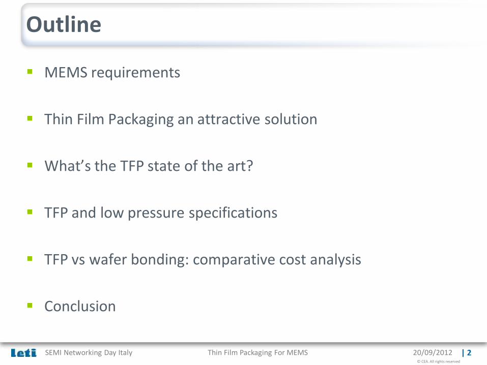
Outline
MEMS requirements
Thin Film Packaging an attractive solution
What’s the TFP state of the art?
TFP and low pressure specifications
TFP vs wafer bonding: comparative cost analysis
Conclusion

© CEA. All rights reserved
SEMI Networking Day Italy Thin Film Packaging For MEMS 20/09/2012 | 3
Leti at a Glance
Founded in 1967 as part of CEA
1,700 researchers
37 start-ups & 265 industrial partners
Over 1,700 patents
250 M€ budget
CEO Dr. Laurent Malier
190 PhD students + 34 post PhD with 70 foreign students (30%)
~ 40M€ CapEx
265 generated in 2010 40% under license
Léti/Minatec at Grenoble (F)
200 and 300mm Si capabities 8,000 m² clean rooms Continuous operation

© CEA. All rights reserved
SEMI Networking Day Italy Thin Film Packaging For MEMS 20/09/2012 | 4
Problematic of MEMS packaging
MECHANICAL
PROTECTION
• Particles
• Humidity
• Vibration
• Mechanical shock
• Thermal stress
• EM waves…
ELECTRICAL IN ELECTRICAL OUT
PHYSICAL / CHEMICAL IN (Sensor)
• Light
• Gas
• Pressure
• Acceleration
• Electromagnetic field…
PHYSICAL OUT (Actuator)
VACUUM GAS FLUID MOVING PARTS
Require specific & complex packages => Important overcost Objective: To manage specificity at the wafer level (collective process)

© CEA. All rights reserved
SEMI Networking Day Italy Thin Film Packaging For MEMS 20/09/2012 | 5
Thin Film Packaging an attractive solution
Many advantages compare to other packaging techniques: Reduced area required for packaging
Very low thickness – tens of µm
Contact pad opening easy – no need for TSV
Process with standard equipments
No need for bonding tool
No need for second wafer
33 % saving
63 % saving

© CEA. All rights reserved
SEMI Networking Day Italy Thin Film Packaging For MEMS 20/09/2012 | 6
Thin Film Packaging categories
Two main types of TFP depending on the sacrificial layers: Mineral sacrificial material (most of the time the same as MEMS)
Organic sacrificial material Resonator TFP with SiO2 sacrificial layer [2] RF switches and accelerometers TFP with SiO2 sacrificial layer [1]
RF variable capacitor with 8 µm polymer sacrificial layer [3]
RF BAW filter with polymer sacrificial layer [4]
RF BAW resonator with polymer? sacrificial layer [5]

© CEA. All rights reserved
SEMI Networking Day Italy Thin Film Packaging For MEMS 20/09/2012 | 7
LETI Thin Film Packaging process flow
LETI mainly focus their developments with organic sacrificial layer to: Minimize the thermal budget of the TFP process (<350 °C)
Be compliant with topology on MEMS substrate
Be less aggressive during the release process
Schematic process flow: Polymer sacrificial layer deposit & patterning
Sacrificial layer curing
Cap deposition
Release hole etching
Cap release
Cap sealing
But what is the state of the art of this technology? Back-end compatibility, mechanical structure, reliability, outgassing…
MEMS wafer
Sacrificial layer
Sensitive part
| 7

© CEA. All rights reserved
SEMI Networking Day Italy Thin Film Packaging For MEMS 20/09/2012 | 8
TFP and Back-end compatibility
Electrical performances on BAW resonator [6]
Same electrical performances before and after TFP + back-end processes
But reinforcement layer mandatory to be compatible with overmolding (100 bars / 200 °C)
TFP UBM process bumping grinding Wafer sawing BAW process
Plaque P02 - Filtre D20_top
cellule C9
-20
-18
-16
-14
-12
-10
-8
-6
-4
-2
0
1.95 2.05 2.15 2.25
F (GHz)
Sdd21 (dB
)
Pack0
Pack1
Pack3
Pack4

© CEA. All rights reserved
SEMI Networking Day Italy Thin Film Packaging For MEMS 20/09/2012 | 9
TFP and Overmolding compatibility
LETI developed different reinforcement processes
BAW resonator electrical performances not affected by 100 bars and 185 °C overmolding [6]
Cap reinforcement with epoxy [6] Cap reinforcement with metal [6]
Resonator + TFP + Cu 23µm
Sacrificial release hole
SiO2 cap
Reinforcement layer
Cap reinforcement with localized metal [7]
Molding epoxy
Cu 23µm
200µm

© CEA. All rights reserved
SEMI Networking Day Italy Thin Film Packaging For MEMS 20/09/2012 | 10
TFP and low pressure specifications
Impact of package miniaturization Pressure increasing can come from:
Outgassing from materials inside TFP cavity (major factor)
µleak
Permeation
Possible schemes to reach low pressure TFP cavities: Optimized materials and outgassing process before sealing the cap
Implement getter materials
120
140
160
080
0
10
00
015
3045
1.0E-02
1.0E-01
1.0E+00
1.0E+01
1.0E+02
Surf
ace
/ V
olu
me
(µm
-1)
Length (µm)Height
(µm)
);( HeightLengthfVolume
Surface
MEMS wafer
Sensitive part
Top surface of the substrate - Passivation (SiO2 or SiN)
- Metal lines (Au, Al…)
Sensitive part of the device
Cap material (SiO2 or SiN) Sealing material

© CEA. All rights reserved
SEMI Networking Day Italy Thin Film Packaging For MEMS 20/09/2012 | 11
TFP and low pressure specifications
Optimized materials and outgassing process before sealing the cap Materials outgassing properties, one of the key parameter [8]
Outgassing properties depend on: material itself, deposition process, thermal and process history...
Outgassing is critical above their thermal deposition temperature (mostly for PECVD materials)
SiN is a good outgassing barrier
Sample
1.E-03
1.E-02
1.E-01
1.E+00
1.E+01
1.E+02
0 50 100 150 200 250 300 350 400 450 500
Thermal treatments (°C/30')
Ou
tgas
sin
g (m
bar
.cm
) Al/TiN SiO2 TEOS
SiN SiO2 HDP

© CEA. All rights reserved
SEMI Networking Day Italy Thin Film Packaging For MEMS 20/09/2012 | 12
TFP and low pressure specifications
Optimized materials and outgassing process before sealing the cap Chemical composition outgassing is another key parameter RGA analysis
mandatory
Sealed MEMS put in a High vacuum chamber
Open cavity in the chamber Analyze gas present
in the chamber
Mass spectrometer
2 benches available at Leti (Resolution N2 0.3 -Ar 0.02pmoles)
Best outgassing process can now be defined (max temperature, temperature ramp up, process time…)
Résiduel_[statique_série5-dynamique_série1]
0.0E+00
1.0E-11
2.0E-11
3.0E-11
4.0E-11
5.0E-11
6.0E-11
5 15 25 35 45
amu
I (A
)
Casse ampoule

© CEA. All rights reserved
SEMI Networking Day Italy Thin Film Packaging For MEMS 20/09/2012 | 13
TFP and low pressure specifications
Implement getter materials
But getter effect depends on gas present inside the cavity (better the outgassing,
better the getter)
Tunable activation temperature (to fit with sealing process)
MEMS wafer
Sensitive part
Getter material is able to pump residual gases [13]
Getter properties
200
250
300
350
400
450
500
0,15 0,2 0,25
N2 sorbing capacity mbar.cm3/cm²
Acti
vati
on
tem
pera
ture
°C
AuSi
AuSn
Anodic
SDB
Leti catalog of getters

© CEA. All rights reserved
SEMI Networking Day Italy Thin Film Packaging For MEMS 20/09/2012 | 14
TFP and low pressure specifications
TFP sealing layer(s) Polymer sealing for device not working under vacuum (i.e BAW)
Metal(s) sealing is the most used sealing layer(s) for vacuum specs
Cap
Polymer
Hole
Release hole sealed
3.0 µm sealing layer
Al sealing materials [8]
Cap
SiO2 sealing
Sealing layers
Ti/Cu sealing materials [7]
Metallic sealing materials [9], [10]

© CEA. All rights reserved
SEMI Networking Day Italy Thin Film Packaging For MEMS 20/09/2012 | 15
Pressure measurement: Q factor monitoring Few results published !
TFP pressure performances summary
TFP without getter TFP
Molecular Glass frit
AuSi
Anodic
AuSn
Wafer bonding techniques
[9]
TFP with getter
10-3 10-2 10-1 1 101 Pressure (mbar)
10-4
Thermal budget (oC)
102 103
[10]
[8]
[11]
[12]
950 oC
[6] [2] [5]

© CEA. All rights reserved
SEMI Networking Day Italy Thin Film Packaging For MEMS 20/09/2012 | 16
Comparative cost analysis
Comparing between Wafer Level Packaging methods Thin film packaging (standard) ~ 30 steps
Thin film packaging (with reinforcement) ~ 40 steps
Si cap packaging (polymer bonding) ~ 40 steps
Si cap packaging (with TSV) ~ 60 steps
Evaluations based on a cost model taking into account: Global process (die area, yields…)
Process flows (equipments CoO, operator time, consumables,…)
Clean room environment (HU, depreciation, footprint, production capacities…)

© CEA. All rights reserved
SEMI Networking Day Italy Thin Film Packaging For MEMS 20/09/2012 | 17
Comparative cost analysis : die area
Layout based on different constraints for the same design rules: • Same electrical contacts geometries (120*120 µm)
excepted for Cap with TSV • Same distances between cutting line and electrodes • Sealing strip 60µm thick
About 20 % gain in die area achieved
Thin film packaging
1000µm X 700µm
Si cap packaging
1100µm X 800µm

© CEA. All rights reserved
SEMI Networking Day Italy Thin Film Packaging For MEMS 20/09/2012 | 18
Comparative cost analysis : results
Thick Cu
ECD
Align /
Bonding
TSV DRIE
Align /
Bonding

© CEA. All rights reserved
SEMI Networking Day Italy Thin Film Packaging For MEMS 20/09/2012 | 19
Conclusion
Today Thin Film Packaging: Low cost packaging technique
Clearly compatible with device working at near atmospheric pressure (depending on the atmosphere specs)
Overmolding compatible
Vacuum packaging demonstrated until 10-3 mbar [9]
Trends: Optimize TFP to be compatible with vacuum devices (gyro, accelero…)
Develop TFP with controlled atmosphere
Perform reliability testing
© CEA. All rights reserved
SEMI Networking Day Italy Thin Film Packaging For MEMS 20/09/2012 | 20
References
[1] V. Rajaraman, "Robust Wafer-Level Thin-Film Encapsulation of Microstructures using Low Stress PECVD Silicon Carbide," Micro Electro Mechanical Systems, 2009. MEMS 2009. IEEE 22nd International Conference on , 25-29 Jan. 2009 [2] Bin Guo et al, "Poly-SiGe-Based MEMS Thin-Film Encapsulation," Microelectromechanical Systems, vol.21, no.1, pp.110-120, Feb. 2012 [3] M. Endo et al, “Low Cost and Reliable Packaging Technology for Stacked MCP with MEMS and Control IC Chips”, Internationale Symposium on Microelectronics, 2009
[4] J.L Pornin et al, "Wafer Level Thin Film Encapsulation for BAW RF MEMS," Electronic Components and Technology Conference, 2007. ECTC '07. Proceedings. 57th , vol., no., pp.605-609, May 29 2007-June 1 2007 [5] K. Seetharaman et al, “A Robust Thin Film Wafer-Level Packaging Approach for MEMS Devices”, IMAPS, 2010
[6] J.L Pornin et al, "Low cost Thin Film packaging for MEMS over molded," Electronic System-Integration Technology Conference (ESTC), 2010 3rd , vol., no., pp.1-4, 13-16 Sept. 2010
[7] J.L Pornin et al, “Cost effective thin film packaging for wide area MEMS”, ECTC, 2012
[8] D. Saint-Patrice et al, "Low temperature sealing process for vacuum MEMS encapsulation," Electronic Components and Technology Conference (ECTC), 2012 IEEE 62nd , pp.97-101, May 29 2012-June 1 2012 [9] G. Dumont et al, “Pixel Level Packaging for uncooled Infrared Focal Plane Array”, MINAPAD, 2011
[10] Y. Naito et al, "High-Q torsional mode Si triangular beam resonators encapsulated using SiGe thin film," Electron Devices Meeting (IEDM), 2010 IEEE International , vol., no., pp.7.1.1-7.1.4, 6-8 Dec. 2010 [11] Dumont G. et al, “Innovative on-chip packaging applied to uncooled IRFPA”, Infrared technology and Applications XXXIV, proc. of SPIE Vol. 6940, 69401Y (2008)
[12] Candler et al, "Long-Term and Accelerated Life Testing of a Novel Single-Wafer Vacuum Encapsulation for MEMS Resonators," Microelectromechanical Systems, Journal of , vol.15, no.6, pp.1446-1456, Dec. 2006
[13] Lionel Tenchine et al, “NEG thin films for under controlled atmosphere MEMS packaging”, Sensors and Actuators A: Physical, Volume 172, Issue 1, December 2011, Pages 233-239