thermoelectric properties in ga2te3 – gasb vacancy …
TRANSCRIPT

THERMOELECTRIC PROPERTIES IN Ga2Te3 – GaSb VACANCY COMPOUNDS
By
Hao Yang
A THESIS
Submitted to Michigan State University
in partial fulfillment of the requirements for the degree of
MASTER OF SCIENCE
Materials Science and Engineering
2011

ABSTRACT
THERMOELECTRIC PROPERTIES IN Ga2Te3 – GaSb VACANCY COMPOUNDS
By
Hao Yang
Thermoelectric materials with high figure of merit, which requires large Seebeck
coefficient, large electrical conductivity and low thermal conductivity, are of great importance in
solid state cooling and power generation. Solid solution formation is one effective method to
achieve low thermal conductivity by phonon scattering due to mass and strain field fluctuation.
This type of scattering is maximized in structures containing vacancies. The thermoelectric
properties of the vacancy compounds of Ga2Te3 – GaSb are studied in this research. We find
that the lattice thermal conductivity is reduced by over an order of magnitude with the addition
of only very moderate amounts of Ga2Te3. Additionally, both the carrier type and concentration
can be modified with the addition of Ga2Te3. While the vacancy structure induced by the
addition of Ga2Te3 to GaSb can effectively reduce phonon conductivity, carrier mobility is also
degraded. Thus the optimized thermoelectric properties require careful control of the vacancy
content in these solid solutions. The effect of preparation methods on thermoelectric properties
of these solid solutions has also been studied. The influence of extrinsic doping and isoelectronic
substitution on thermoelectric performance of Ga2Te3 – GaSb is also discussed in this work.
ii

ACKNOWLEDGEMENTS
First of all, I want to express my sincere appreciation to my research advisor Dr. Donald
Morelli who gives me great guidance, support and encouragement on my study in his group. His
expertise in Thermoelectric materials and instructions on my research project helps me to make
continuous progress on my graduate study. Thanks are also given for his efforts on this thesis
paper. I believe that the valuable things I learned from Dr. Donald Morelli during the graduate
study experience will benefit my whole life.
I also want to thank my committee members, Dr. Sakamoto and Dr. Lai, for their support
and evaluation on my thesis paper and final defense. Thank you all for your time and effort on
my graduate research. Thanks are also given to all my group members for your help and support
for my research. The priceless working experience with you will influence my entire life
definitely.
Thank all the staff in department of Chemical Engineering and Materials Science. Your
grateful effort helps me go through all the administrative process and ensures my graduation.
iii

TABLE OF CONTENTS
LIST OF TABLES………………………………………………………………………………...v
LIST OF FIGURES...…………………………………………………………………………….vi
CHAPTER 1 Introduction to Thermoelectric materials…..……………………………………..1 1.1 Thermoelectric phenomena……………………………………………………………….1 1.2 Thermoelectric circuit…………………………………………………………………….2 1.3 Energy conversion efficiency and thermoelectric figure of merit………………………..3 1.4 Design of thermoelectric materials…………………………………………………….....5 1.5 Promising thermoelectric materials and application…………………………………….10
CHAPTER 2 Vacancy compounds as thermoelectric materials...…………………………..….12 2.1 Introduction of vacancy compounds……………………………..……….……………..13 2.2 A new kind of vacancy compound: Ga2Te3 – GaSb………………………………….18 2.3 Thermoelectric properties of Ga2Te3 – GaSb…………………..……………………...21 2.4 Effect of preparation method on thermoelectric properties of Ga2Te3 – GaSb………40
CHAPTER 3 Effect of doping on thermoelectric properties of Ga2Te3 – GaSb..…………...47 3.1 Thermoelectric properties of Zinc-doped samples………………………………...……47 3.2 Effect of isoelectronic substitution on Thermoelectric properties……………………....53
CHAPTER 4 Conclusion…..…………………………………..……………………………….60
BIBLIOGRAPHY………………………...…………………………………………………...…62
iv

LIST OF TABLES
Table 1 Melting temperature of these pure elements and compounds…………………………...22
Table 2 Type of semiconductor of (Ga2Te3)x(Ga3Sb3)1-x with different content of Ga2Te3…..26
v

LIST OF FIGURES
Figure 1 Thermoelectric circuits for heating/cooling (a) and power generation (b)………………3
Figure 2 Nominal dependencies of the Seebeck coefficient, electrical conductivity, and power factor on carrier concentration in a solid………………………………………………………….5
Figure 3 Common n- (a) and p-type (b) thermoelectric materials……………………………….10
Figure 4 The zinc-blende structure of InSb……………………………………………………...13
Figure 5 Dependence of κL on content of In2Te3…………….………….…………………..…15
Figure 6 Temperature dependence of κL……………………...…………………………………15
Figure 7 The band structure of InSb and GaSb…………………………………………………..17
Figure 8 TEM image of Ga2Te3…………………………...…………………………………….18
Figure 9 Temperature dependence of thermal conductivity of In2Te3 and Ga2Te3. Balls and lines represent the measured and minimum κ values, respectively. Violet and orange symbols represent the results for Ga2Te3 and In2Te3, respectively………………………..…………..…19 Figure 10 XRD patterns for (Ga2Te3)x(Ga3Sb3)1-x with different content of Ga2Te3…………24
Figure 11 Dependence of lattice constant of (Ga2Te3)x(Ga3Sb3)1-x on content of Ga2Te3……25
Figure 12 Dependence of lattice thermal conductivity of (Ga2Te3)x(Ga3Sb3)1-x on temperatur.27
Figure 13 Dependence of lattice thermal conductivity on content of Ga2Te3 at 80K and 300K..28
Figure 14 Temperature dependence of resistivity of (Ga2Te3)x(Ga3Sb3)1-x…………….……...29
Figure 15 Temperature dependence of carrier concentration of (Ga2Te3)x(Ga3Sb3)1-x………..30
Figure 16 Temperature dependence of mobility of (Ga2Te3)x(Ga3Sb3)1-x…………………….32
vi

Figure 17 Dependence of the value of μ/κL on content of Ga2Te3………………………….…33
Figure 18 Temperature dependence of Seebeck coefficient of (Ga2Te3)x(Ga3Sb3)1-x………...34
Figure 19 Dependence of reduced Fermi energy (η) on Ga2Te3 content………………………..35
Figure 20 Dependence of effective mass on Ga2Te3 content……………………………………35
Figure 21 Dependence of weighted mobility (μ*) on content of Ga2Te3……………………...36
Figure 22 Dependence of F factor on content of Ga2Te3………………………………………..37
Figure 23 Temperature dependence of power factor of (Ga2Te3)x(Ga3Sb3)1-x………………..38
Figure 24 Temperature dependence of figure of merit of (Ga2Te3)x(Ga3Sb3)1-x……………...39
Figure 25 XRD patterns for (Ga2Te3)0.05(Ga3Sb3)0.95 with different synthesis methods…...41
Figure 26 Temperature dependence of lattice thermal conductivity of (Ga2Te3)0.05(Ga3Sb3)0.95 with different synthesis methods………………………………………………………………...43 Figure 27 Temperature dependence of resistivity of (Ga2Te3)0.05(Ga3Sb3)0.95 with different synthesis methods………………………………………………………………………………..43
Figure 28 Temperature dependence of carrier concentration……………………………………44
Figure 29 Temperature dependence of mobility…………………………………………………45
Figure 30 Temperature dependence of Seebeck coefficient of (Ga2Te3)0.05(Ga3Sb3)0.95 with different synthesis methods………………………………………………………………………45 Figure 31 Temperature dependence of power factor of (Ga2Te3)0.05(Ga3Sb3)0.95 with different synthesis methods………………………………………………………………………………..46 Figure 32 Temperature dependence of figure of merit of (Ga2Te3)0.05(Ga3Sb3)0.95 with different synthesis methods………………………………………………………………………………..46 Figure 33 XRD patterns of the zinc-doped samples……………………………………………..48
vii

Figure 34 Dependence of lattice constant of zinc-doped samples on content of Zn…………….49
Figure 35 Temperature dependence of lattice thermal conductivity of zinc-doped samples……49
Figure 36 Temperature dependence of Seebeck coefficient of zinc-doped samples…………….50
Figure 37 Temperature dependence of carrier concentration of zinc-doped samples…………...51
Figure 38 Temperature dependence of mobility of zinc-doped samples………………………..51
Figure 39 Temperature dependence of resistivity of zinc-doped samples………………………52
Figure 40 Temperature dependence of figure of merit of zinc-doped samples………………….52
Figure 41 XRD patterns of samples with indium substitution…………………………………..54
Figure 42 Dependence of lattice constant on content of indium………………………………...55
Figure 43 Temperature dependence of lattice thermal conductivity of samples with indium substitution……………………………………………………………………………………….56 Figure 44 Temperature dependence of Seebeck coefficient of samples with indium substitution…………………………………………………………………………56 Figure 45 Temperature dependence of carrier concentration of samples with indium substitution…………………………………………………………………………57 Figure 46 Temperature dependence of resistivity of samples with indium substitution………...58
Figure 47 Temperature dependence of power factor of samples with indium substitution……...58
Figure 48 Temperature dependence of figure of merit of samples with indium substitution……59
viii

CHAPTER 1 Introduction to Thermoelectric Materials
With the rise in demand for energy and the increase in environmental problems caused by
combustion of fossil fuels over the world, the thermoelectric materials are receiving more and
more attention in recent years. Home heating, vehicle exhaust and industrial processes all
generate enormous amount of heat. In our daily life, two third of the energy is emitted in the
form of heat which results not only in the pollution of the environment, but also huge energy
waste. Thermoelectric materials, which can absorb and liberate heat under current excitation and
convert thermal energy into electric energy, are regarded as an environment-friendly solution to
increasing energy efficiency.
1.1 Thermoelectric phenomena
The thermoelectric effect is a thermodynamically reversible process in conductors with
flows of heat and electricity. The most important effects in thermoelectric phenomena are
Seebeck effect, Peltier effect and Thomson effect.
The Seebeck effect was discovered by Thomas J. Seebeck in 1823. When a closed circuit is
composed of two different kinds of conducting materials and the junctions are at different
temperatures, an electromotive force will be observed between the two junctions and a current
will be detected in the circuit. This electromotive force is called the Seebeck electromotive force
and can be expressed by equation 11:
AB ABE S T= ×Δ (1)
where SAB is the relative Seebeck coefficient between the conducting material A and B.
1

The Peltier effect is a reverse process of Seebeck effect which was discovered by Jean C.A.
Peltier in 1834. When a current is introduced into a closed circuit composed of two
different kinds of conducting materials, heat is absorbed at one junction and liberated at
the other. The heat absorbing rate is proportional to the current which is expressed by equation
21:
AB ABQ π= I (2)
where πAB is the relative Peltier coefficient between material A and B.
The Thomson effect is discovered by William Thomson, who examined the effects of
Seebeck and Peltier and concluded that a relation exists between these two coefficients which is
expressed by equation 31:
T Sπ = × (3)
The Thomson effect is a thermodynamically reversible process of heat absorbing and
liberating in a circuit consisting of a single homogenous conducting material, rather than two
conductors, when a current and a temperature gradient is in present.
1.2 Thermoelectric circuit
The thermoelectric effects are utilized in the thermoelectric circuit which consists of p-type
and n-type semiconducting materials, as is shown in Figure 12.
2
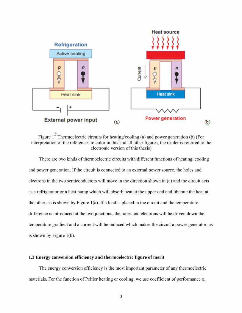
Figure 12 Thermoelectric circuits for heating/cooling (a) and power generation (b) (For interpretation of the references to color in this and all other figures, the reader is referred to the
electronic version of this thesis)
There are two kinds of thermoelectric circuits with different functions of heating, cooling
and power generation. If the circuit is connected to an external power source, the holes and
electrons in the two semiconductors will move in the direction shown in (a) and the circuit acts
as a refrigerator or a heat pump which will absorb heat at the upper end and liberate the heat at
the other, as is shown by Figure 1(a). If a load is placed in the circuit and the temperature
difference is introduced at the two junctions, the holes and electrons will be driven down the
temperature gradient and a current will be induced which makes the circuit a power generator, as
is shown by Figure 1(b).
1.3 Energy conversion efficiency and thermoelectric figure of merit
The energy conversion efficiency is the most important parameter of any thermoelectric
materials. For the function of Peltier heating or cooling, we use coefficient of performance ϕ,
3

which is rate of absorption or evolution of heat at certain temperature divided by total electric
power consumed, to define the conversion efficiency3:
max
( 1 1) 12( 1 1)
ave ave
ave
T ZTT ZT
φ+ −
= −Δ + + (4)
For the function of power generation, the efficiency is defined as useful electric power I2R
delivered to the external circuit divided by the rate of heat energy absorption at the source
temperature3:
1 11
ave
H ave C H
ZTTT /ZT T T
ε+ −Δ
=+ + (5)
Equation 5 shows that, with increasing value of ZTave, the energy conversion efficiency reaches
its maximum of Carnot efficiency.
For both case of Peltier heating or cooling and power generation, the energy conversion
efficiency increases with increasing ZT. ZT is dimensionless value which is called the figure of
merit:
2S PZT Tσκ κ× T= × = × (6)
where S is Seebeck coefficient, σ is electrical conductivity, κ is thermal conductivity, T is
absolute temperature, P is called the power factor. So the main objective of study about
thermoelectric materials is to increase the figure of merit so as to achieve higher conversion
efficiency.
4

1.4 Design of thermoelectric materials
The figure of merit consists of three parts: Seebeck coefficient, electrical conductivity and
thermal conductivity. Large Seebeck coefficient can maintain large electromotive force between
the two junctions at certain temperature difference, which increases the electric power output at
given rate of heat absorption. High electrical conductivity, that is low resistivity, can minimize
the Joule heat generated by the conductors which decreases the energy loss and increases the
energy conversion efficiency. Small thermal conductivity can prevent the temperature difference
between the junctions from decreasing due to the thermal flow along the conductors. The
maintained temperature difference can help to generate the electromotive force by Seebeck effect
and convert thermal energy into electrical energy.
The relation between Seebeck coefficient and electrical conductivity and the value of
power factor is shown in figure 24. The Seebeck coefficient will decrease with the increasing
electrical conductivity. So the highest power factor is achieved in the region of semiconductor.
Figure 24 Nominal dependencies of the Seebeck coefficient, electrical conductivity, and power factor on carrier concentration in a solid
5

In intrinsic semiconductors, the Seebeck coefficient could be expressed by equation 75:
e e h h
e h
S SS σ σσ σ
+=
+ (7)
where Se/Sh is the Seebeck coefficient of electron/hole, σe/σh is the conductivity of electron/hole.
Because Se is negative and Sh is positive, the coexistence of electron and hole will decrease S.
Extrinsic doping of semiconductors can increase the concentration of one kind of charge carriers
and almost eliminate the other which will prevent the compensation of Seebeck coefficient by
electrons and holes. In a doped semiconductor, the Fermi level is close to or even within the
conduction band which makes the semiconductor partially degenerate. In this case, the carrier
concentration should be expressed by equation 8 under the condition of Fermi-Dirac distribution
rather than Boltzmann distribution5:
*3/2
1/22
24 ( )Bm k Tn Fh
ππ
= (8)
where m* is carrier effective mass and F1/2 is Fermi integral in the form of:
0 1 exp( )
r
rxF dx
x η
∞
=+ −∫ (9)
The Seebeck coefficient can be expressed by equation 105:
3/2
1/2
5( )23( )2
BFkS
e F
λ
λ
λη
λ
+
+
⎡ ⎤+⎢ ⎥= −⎢ ⎥
⎢ ⎥+⎣ ⎦
∓ (10)
6

where η is reduced Fermi energy which equals to EF/kBT and λ is carrier scattering parameter
which equals -1/2 for lattice scattering and +3/2 for ionized impurity scattering. From equation 8
to 10, we can see that the value of S2n is only controlled by the location of Fermi level (η), the
nature of electron scattering (λ) and carrier effective mass (m*). The maximum of S2n is
achieved when Fermi level slightly shifts into the conduction band, which indicates a partially
degenerate semiconductor5.
The electrical conductivity is defined by equation 11:
neσ μ= (11)
where μ is carrier mobility. Large carrier effective mass may result in high carrier concentration,
but also low mobility, because heavy carriers move at low speed. Equation 6 shows that the
power factor equals (S2σ), that is (S2neμ). The value of n×μ leads to the concept of effective
mobility which is expressed by equation 12:
* *( )mμ μ= 3/2 (12)
The semiconductor with high effective mobility will have large electrical conductivity.
Thermal energy in solids is transferred primarily by electrons and phonons. So the thermal
conductivity κ consists of two parts: κE – electronic thermal conductivity and κL – lattice thermal
conductivity. The electronic thermal conductivity is related to electrical conductivity by
Wiedemann-Franz law6:
E L Tκ σ= (13)
7

where L is the Lorentz constant. The value of lattice thermal conductivity is usually obtained by
subtracting electronic thermal conductivity from the total thermal conductivity. The lattice
thermal conductivity could also be expressed by equation 141:
13L v ph phC lκ ν= (14)
where Cv is heat capacity per unit volume, νph is phonon velocity, lph is phonon mean free path
which is equal to phonon velocity times relaxation time for phonon scattering process τ. Phonons
in the lattice can be scattered by other phonons, point defects, grain boundaries, charge carriers
and so on. The total rate of scattering process, which is the reciprocal of relaxation time τ, equals
to the sum of that of different scattering process7.
1 1 1 1 1int ...i phonon phonon po defect grain boundary
iτ τ τ τ τ− − − − −
− − −= = + + +∑ (15)
At high temperature, which is near or above Debye temperature, the phonon – phonon
scattering process is predominant. The specific heat is constant at the Dulong-Petit value and the
mean free path decreases exponentially with temperature. So the lattice thermal conductivity
decreases with increasing temperature. At low temperature, which is well below Debye
temperature, the grain boundary scattering is predominant. The mean free path is constant and
equals to the grain size, and the specific heat is proportional to T3 at low temperature. So the
lattice thermal conductivity increases as T3. As is pointed out above, the lattice thermal
conductivity over Debye temperature will decrease with increasing temperature due to the
increasing of intensity of vibrations of the lattice. So, at certain temperature, the lattice thermal
8

conductivity should be smaller for the material with lower Debye temperature. The Debye
temperature for an element or compound will decrease with increasing atomic weight, which
indicates that, for the elements in the same column of the periodic table, the element with higher
atomic weight will have the lower lattice thermal conductivity3.
For the point defect scattering of phonons, the scattering rate is proportional to the
concentration of the impurity atom and the square of mass difference between host lattice atom
and the impurity atom. So an effective method to increase the phonon scattering by point defect
is to make isoelectronic substitution for the host atom with the impurity atom of very different
mass.
Because the Seebeck coefficient and carrier concentration could be expressed by Fermi
level and the nature of electron scattering, we can write the equation for figure of merit in terms
of reduced Fermi energy and electron scattering parameter5:
2
12
5( )2
52 exp (2
B
zk FG Te
λ η
)η λ−
+ −=⎛ ⎞
+ +⎜ ⎟⎝ ⎠
(16)
where * 3/2( )
L
F mμκ
= (17)
3/2
2
2 Bmk TGh
π⎛ ⎞= ⎜⎝ ⎠
⎟ (18)
Equation 16 shows that that the value of figure of merit depends on the reduced Fermi
energy, the electron scattering parameter and factor F. The Fermi level could be
controlled and optimized by doping. The variation of electron scattering parameter is small. So
the predominant factor to determine the plausibility of thermoelectric application is the value of
F, which requires large effective mobility and small lattice thermal conductivity.
9

In conclusion, the three parameters of Seebeck coefficient, electrical conductivity and
thermal conductivity are interrelated, it is difficult to change one without affecting the other two.
The most effective way to improve ZT is to use the semiconducting materials with high effective
mobility and optimize the Fermi level by doping to achieve large power factor, and at the same
time, to scatter phonons (but not electrons) by point defects, grain boundaries, charge carriers,
and so on to decrease lattice thermal conductivity without affecting carrier mobility significantly.
1.5 Promising thermoelectric materials and application
In the past decades of research, several promising thermoelectric materials have been
developed in the laboratory and applied to industrial and commercial use.
Figure 38 Common n- (a) and p-type (b) thermoelectric materials
As is shown by Figure 38, for room temperature application, the most widely used
thermoelectric material is the alloys of Bi2Te3 and Sb2Te3 with the peak ZT value
between 0.8 to 1.1. For mid-temperature application (500 ~ 1000 K), the state-of-the-art
materials are PbTe and skutterudite materials. These skutterudite materials are in the form of
AB3 (A=Co, Ni, Fe; B=P, Sb, As) with cage-like structure into which some low-coordination
10

ions, like rare-earth elements, can be filled. The filled atoms will “rattle” within the cage to
scatter phonons so as to reduce the thermal conductivity but not affect the electron mobility very
much9. The solid solution of Ge-Si is suitable for high temperature application (over 1000 K).
With the development of nanotechnology, researchers have achieved enhanced ZT in some new
materials such as nanocomposites, superlattice thin films, quantum dot superlattices, and
nanowires.
Thermoelectric devices are solid-state devices. They are reliable, scalable, silent and
environment-friendly. They have no moving parts and do not require refrigerant liquids, such as
chlorofluorocarbons, for cooling. They could be applied as thermoelectric generators in the
vehicle exhaust pipe or radioisotope thermoelectric generator in aerospace applications. They
could be used as thermocouples and thermopiles for temperature measurement. Thermoelectric
materials can also be used as refrigerators, such as the climate control seat in vehicles. With
further investigation, more promising TE materials and application will be found in the future.
11

CHAPTER 2 Vacancy compound of thermoelectric materials
Since the total thermal conductivity has electron and lattice components and the electrical
thermal conductivity is related to the electrical conductivity by Wiedemann-Franz law, so an
effective method to decrease thermal conductivity is to minimize κL by scattering phonons.
There are several different phonon scattering mechanisms in materials including phonon-phonon
scattering, grain boundary scattering, point defect scattering, resonance scattering and charge
carrier scattering, and the total rate of scattering equals to the sum of that of different processes7.
Solid solution formation is one effective way to achieve low thermal conductivity because of
point defect scattering which is caused by the mass and strain filed fluctuation10,11. It is proved
that the atomic mass difference between the guest and the host and the concentration of the
impurity play an important role in the reduction of κL. The scattering parameter A can be
expressed by equation 196:
202 (1 )( )
4MA x x
v MπΩ Δ
= − (19)
where Ω0, ν, x, ΔM, and M stand for the volume of the unit cell, the lattice sound velocity, the
fraction of guest atom, the atomic mass difference between the guest and the host and the
average mass of the cell respectively. The lattice thermal conductivity is inversely proportional12
to A1/2. The solid solution of compounds with same crystal structure can help to reduce the
lattice thermal conductivity. The isoelectronic substitution, which means the guest and host atom
have the same valence, can further increase the figure of merit by preventing the mobility from
decreasing. Because the replacing atom remains neutral in the lattice, there is no Coulomb force
12

that will scatter electrons thus to decrease the electrical conductivity. The examples of solid
solution involving isovalent substitution are InSb – GaSb and GaAs – GaSb.
2.1 Introduction of vacancy compound
A vacancy compound is one kind of solid solution with some lattice sites vacant or
unoccupied by atoms. Under such a condition, the value of ΔM/M is maximized at a value of
unity13, and this kind of defect structure can be achieved on many lattice sites throughout the
crystal, so we can expect strong phonon scattering by point defect in vacancy compound.
Figure 4 The zinc-blende structure of InSb
The solid solution of In2Te3 – InSb is one kind of vacancy compound. InSb is a
semiconducting material for infrared detector application, like thermal imaging cameras. InSb
possesses the zinc-blende structure. As is shown by figure 4, the lattice sites of the face-centered
cubic system are occupied by antimony atoms and the four interstitial sites which are not
adjacent are occupied by indium atoms. InSb has excellent power factor due to its highest carrier
mobility among all the III – V semiconductors, which is about 80000 cm2/V*s7,14. But the large
thermal conductivity of pure InSb at both low and high temperature makes it inappropriate for
13

the thermoelectric application6. The compound of In2Te3 also possesses the zinc-blende
structure with one lattice site in three on the indium sub-lattice vacant, which means one in every
three of the interstitial sites is not occupied by indium atom15,16. Because one vacancy defect is
achieved in every three indium sub-lattices throughout the crystal and the value of ΔM/M from
equation 19 equals unity, the lattice thermal conductivity of In2Te3 is very low compared with
that of InSb due to the strong phonon scattering by these vacancy point defects. A solid solution
of In2Te3 and InSb will introduce the vacancy structure into the material to scatter phonons more
effectively thus to decrease the lattice thermal conductivity greatly, and at the same time,
optimize the carrier concentration of InSb so as to achieve higher power factor. It is reasonable
to expect this formation of solid solution with vacancies can improve the thermoelectric
performance.
The stoichiometric composition of this solid solution is (In2Te3)x(In3Sb3)1-x, and several
researchers6,17,18 have demonstrated that the solid solution of In2Te3-InSb also crystallizes in
the zinc-blende structure with solubility of In2Te3 up to 15 mol% (x=0.15). The addition of
In2Te3 increases the phonon scattering effect by point defect and thus greatly decreases the
lattice thermal conductivity both at low and room temperature. Figure 56 shows the change of κL
of different In2Te3 content at 80 K and 300 K respectively. Because the mass and atomic size
difference between antimony and tellurium is negligible, little mass and strain field fluctuation is
caused by just replacing antimony atom with tellurium atom, so the obvious reduction of κL
should be due to the occurrence of vacancy structure.
14

ΚL
ΚL
Figure 56 Dependence of κL on content of In2Te3 Figure 66 Temperature dependence of κL
Because Te atom has one more valence electron than Sb atom, the addition of In2Te3 into
InSb not only introduces vacancy structure but also dopes the solid solution n-type19. So this
solid solution becomes n-type and the electron concentration6 in InSb increases from ~1016 to
~1019 cm-3. The increasing carrier concentration can improve the electrical conductivity, but the
Seebeck coefficient will decrease with the increasing σ. Additionally, an increase of σ increases
the electronic thermal conductivity, which leads to the increasing of total thermal conductivity
and reduction of ZT. Some researchers6 studied the deficiency on the In site, which is in the
stoichiometric composition of (In2.85)1-δSb2.55Te0.45. This will result in an even higher vacancy
concentration to scatter phonons so as to further reduce lattice thermal conductivity. And because
both InSb and In2Te3 are ionic compounds, the decreasing amount of In atom will reduce the
electrons contributed to the conduction band. The deficiency on the In sites further reduces the
15

thermal conductivity, decreases the carrier concentration and optimizes the Fermi level to
achieve higher power factor, which results in an enhanced ZT. Figure 66 shows the temperature
dependence of κL for InSb, In2.85Sb2.55Te0.45, (In2.85)1-δSb2.55Te0.45 and a typical PbTe. As
can be seen from figure 6, the κL of (In2.85)1-δSb2.55Te0.45 is further reduced and can be
comparable to that of the typical state-of-art TE materials, PbTe.
The vacancy compound of In2Te3-InSb can achieve higher figure of merit because of
effective phonon scattering by vacancies. But there are still some disadvantages of this solid
solution. The lattice vacancy in In2Te3 is disordered. Although the vacancy can be transformed
to order at temperature of approximately 893 K20,21,22, this ordering requires special preparation
techniques or very long annealing time because of the low diffusivity23. This will increase the
cost and complexity of manufacture process. If the lattice vacancy is disordered, there will be
additional scattering center in the materials that lower both the thermal conductivity as well as
the electron mobility. The reduced mobility will decrease the electrical conductivity which will
harm the ZT. But an ordered state of vacancy, on the other hand, can increase the mobility24 and
the energy gap25,26,27 which is due to the reduction in entropy and increment in strength of
some bonds. The ordering vacancy can improve electrical conductivity and power factor without
increasing thermal conductivity. But it is very difficult to achieve ordering state in In2Te3
unfortunately.
Another disadvantage of this solid solution is the low solubility of In2Te3 which is only 15
mol%. Because every three sites on the In sub-lattice contributes one vacancy, the actual vacancy
16

concentration is only 5 mol%. If we can increase the vacancy concentration by finding another
solid solution with higher solubility, we can improve the effect of phonon scattering and further
reduce the thermal conductivity.
Figure 7 The band structure of InSb and GaSb
InSb has a narrow band gap which is only 0.17 eV at room temperature17. As is shown by
figure 7, this narrow band gap allows for little control of its electronic properties near and above
room temperature. With narrow band gap, the electrons in the valence band will be excited into
the conduction band easily. So the temperature for intrinsic conduction is relatively low and that
will decrease the temperature range for extrinsic conduction. Besides, when an electron is
excited into conduction band, a hole will be left in the valence band. With the increasing of
intrinsic carrier concentration, there will be two types of carrier, electron and hole, in this
material. As is shown by equation 7, Seebeck coefficient will be decreased because of the
compensation. The narrow band gap often leads to small effective mass28 which results in low
carrier concentration, as is shown by equation 8.
17

2.2 A new kind of vacancy compound: Ga2Te3 – GaSb
The structure and thermoelectric properties of Ga2Te3-GaSb is similar to that of In2Te3-
InSb. Ga2Te3 also has a defect zinc-blende structure with one in every three sites on the gallium
sub-lattice vacant29. But compared with In2Te3-InSb, the solid solution of Ga2Te3-GaSb has
several advantages.
Kurosaki20 reports that, in the materials of Ga2Te3 prepared by hot pressing, regularly
arranged two dimensional vacancy planes are detected throughout the whole area of the sample,
which is shown in Figure 820. These vacancy planes exist along all four [111] directions with
approximately 3.5 nm intervals. Kurosaki also reports that, compared with In2Te3, Ga2Te3 with
the 2D vacancy planes can scatter phonons more effectively.
Figure 820 TEM image of Ga2Te3
18

The molecular weight of In2Te3 (612.4) is heavier than that of Ga2Te3 (522.24), and the
Debye temperature evaluated from the sound velocity of In2Te3 (159 K) is lower than that of
Ga2Te3 (245 K)20. So the thermal conductivity of In2Te3 should be lower than that of Ga2Te3,
but the result is opposite. As can be seen from figure 920, the thermal conductivity of Ga2Te3 is
lower which indicates a highly effective phonon scattering mechanism related to ordering
vacancies. The ordering state of the vacancy, such as regularly arranged vacancy planes, can also
increase the mobility. With increased electric conductivity and reduced thermal conductivity,
Ga2Te3 can achieve higher ZT value.
Figure 920 Temperature dependence of thermal conductivity of In2Te3 and Ga2Te3. Balls and lines represent the measured and minimum κ values, respectively. Violet and orange symbols
represent the results for Ga2Te3 and In2Te3, respectively
Another advantage is that GaSb possesses a wider band gap, which is 0.72 eV at room
temperature7. The wider band gap increases the temperature range for extrinsic conduction and
19

makes it easier to control the electronic properties by doping. With increasing band gap, there
will be fewer intrinsic electrons excited into the conduction band, and the holes left in the
valence band will also be fewer in number. This will prevent the Seebeck coefficient from
decreasing at high temperatures due to mixed carrier conduction.
The electron effective mass of GaSb which is 0.042 m0, is higher than that of InSb, which
is only 0.014 m07. The electron kinetic energy can be expressed as:
2 2
*2kkEm
= (20)
So the carrier effective mass is inversely proportional to the second derivative of Ek, which is
also the curvature of conduction band:
2* 2
2( )kd Emdk
1−= (21)
As is shown by Figure 7, GaSb with large carrier effective mass has flat conduction band
edge. From equation 10, we can see that Seebeck coefficient depends only on the location of
Fermi level and electron scattering parameter. In the condition of same value of Fermi energy
and Seebeck coefficient, GaSb with flat conduction band edge possesses larger gray area which
indicates higher carrier concentration. This result agrees with equation 8 that large effective mass
leads to high carrier concentration.
The solubility of Ga2Te3-GaSb at 773K extends to 36mol% of Ga2Te319 which is greater
than that of In2Te3-InSb. The stoichiometric composition of this solid solution is
(Ga2Te3)x(Ga3Sb3)1-x, so the vacancy concentration will be up to 12 mol%. The higher vacancy
20

concentration can help to scatter phonons more effectively so as to achieve better TE
performance.
There are also some disadvantages of the solid solution of Ga2Te3-GaSb. Both GaSb and
Ga2Te3 are initially p-type semiconductors30. The effect of adding Ga2Te3 not only introduces
vacancies into the solid solution, but also allows for some Te atoms to replace Sb atoms and thus
dope the material n-type. So this solid solution, at least for some compositions, shows mixed
carrier conduction19. Mixed n-type and p-type conduction leads to compensating effects which
partially cancel out the induced Seebeck voltage8.
Although Ga2Te3 contains regularly arranged 2D vacancy planes, the doping with GaSb
might affect the formation of the vacancy plane and the crystal symmetry31,32. The effect of
Ga2Te3 concentration on the formation of ordering state of vacancy needs further investigation.
2.3 Thermoelectric properties of Ga2Te3 – GaSb
The solid solution of Ga2Te3 – GaSb with a composition of (Ga2Te3)x(Ga3Sb3)1-x were
prepared by the vacuum melting method. The melting temperatures of these pure elements and
compound are displayed in Table 1. As can be seen from Table 1, the melting point for pure
gallium is only 303 K which is much lower than others. The stoichiometric quantities of the three
pure elements of gallium, antimony and tellurium were put into a quartz ampoule and then the
ampoule was sealed under vacuum. The ampoule was vertically hung into a tube furnace. The
sample was heated to 1173 K with the heating rate of 1 K/min and soaked at that temperature for
21

about 20 hours to mix all the elements homogeneously in the liquid phase. The slow heating rate
of 1 K/min is adopted to prevent volatilization of the elements. Then the sample is slow cooled to
873 K in the furnace with the cooling rate of 0.2 K/min and held at that temperature to anneal for
3 days. After 3 days annealing the sample is cooled down to room temperature with the rate of
0.5 K/min in the furnace. Because of the poor mechanical properties of gallium, the sample
prepared by vacuum melting method often contains tiny cracks throughout the body. So the slow
cooling rate is applied to minimized the cracks in the sample and prevent the ampoule from
explosion due to fast cooling. Another reason for the slow cooling rate is to increase the grain
boundary size so as to decrease the effect of grain boundary scattering of phonons. The fast
cooling process, such as quenching, will decrease the grain boundary size. Because the objective
of the research is to study the effect of vacancy structure on the reduction of lattice thermal
conductivity, we want to minimize the contribution of grain boundary scattering of phonons. All
the samples, including the zinc and indium doped samples described in chapter 3, are prepared in
the same way.
Table 1 Melting temperature of these pure elements and compounds
Materials Gallium Antimony Tellurium GaSb Ga2Te3
Melting temperature (K) 303 903 723 985 1065
The resulting ingot was cut by low diamond saw into rectangular parallelepiped with
dimensions of 3×3×8 mm3 for thermoelectric property measurement. Additionally, a small piece
of the sample was pulverized to prepare a powder for structural characterization. The crystal
structure of the sample is measured by powder X-ray diffraction analysis using Miniflex II
Desktop X-ray Diffractometer produced by Rigaku Corporation. The electrical and thermal
22
properties were measured by bath-type cryostat. The sample was tested under vacuum and
measured from 80 K to 300 K using liquid nitrogen as refrigerant. Two thermocouples of copper
– constantan were soldered to the sample at two points along its length; these thermocouples are
used to measure the temperature difference long the sample. One end of the sample is attached to
an 800 Ω resistor which acts as a heater, the other is soldered directly to the copper cold tip of
the cryostat. The electrical conductivity is measured by passing current through the sample and
recording the voltage between the two copper legs of the thermocouples. When energizing the
resistor with current, heat is developed and flows down the sample length. After a steady state is
reached, the thermocouples detect the temperature difference which is used to calculate the
Seebeck coefficient. The thermal conductivity is calculated by the resistor power, temperature
difference and sample dimensions. The carrier concentration and carrier mobility are measured
on small Hall bars cut from the same ingot from -3T to +3T using a VersaLabTM produced by
Quantum Design, Inc.
23

Figure 10 XRD patterns for (Ga2Te3)x(Ga3Sb3)1-x with different content of Ga2Te3
As reported by Woolley19, the solubility of Ga2Te3 in GaSb can reach up to 36 mol%.
Therefore, solid solutions in the composition of (Ga2Te3)x(Ga3Sb3)1-x with x varying from 0 to
0.36 are prepared by vacuum melting method. Figure 10 shows that, the samples with the content
of Ga2Te3 up to 25 mol% possess the single phase of zinc-blende structure. For the samples with
30 mol% and 36 mol% of Ga2Te3, impurity phases are detected around the (111) peak, as is
indicated by black dots. Woolley reported that the single phase of the solid solution with 36
mol% of Ga2Te3 is achieved after 12 month of annealing at 773 K. So the occurrence of
24

impurity phase for the present samples with high Ga2Te3 content might be due to the insufficient
annealing time which in the present case is only 3 days.
6.04
6.05
6.06
6.07
6.08
6.09
6.1
0 0.05 0.1 0.15 0.2 0.25 0.3
Content of Ga2Te3
Latti
ce C
onst
ant (
Å)
Figure 11 Dependence of lattice constant of (Ga2Te3)x(Ga3Sb3)1-x on content of Ga2Te3
Figure 11 shows that lattice constant of this solid solution with different content of Ga2Te3.
The lattice constant of pure GaSb is 6.093 Å and that of pure Ga2Te3 is 5.898 Å33. According to
the Vegard’s Law, the lattice constant should decrease with increasing amount of Ga2Te3. From
Figure 11, the lattice constant decreases linearly with the content of Ga2Te3 increasing to 0.15,
which indicates that all the Ga2Te3 goes into the lattice of GaSb in this composition range. When
the content of Ga2Te3 is higher than 0.15, the lattice constant saturates, suggesting that a
solubility limit has been exceeded in this range. These results are consistent with the onset of
impurity phase that we see at high Ga2Te3 concentration.
25

Both GaSb and Ga2Te3 are initially p-type semiconductors. Because the Te atom has one
more valence electron than the Sb atom, we expect that adding Ga2Te3 into GaSb will dope the
semiconductor to n-type as Te atoms replace some Sb atoms. The hole concentration of pure
GaSb sample at 300 K is 3.3×1017 cm-3, while the sample with 4 mol% of Ga2Te3 is n-type with
an electron concentration at 300 K of 3.7×1018 cm-3. Table 2 shows the type of semiconductor
with different content of Ga2Te3. With increasing Ga2Te3 concentration, the electron
concentration decreases. When x=0.07, the electron concentration decreases to 1.23×1018 cm-3
at 300 K. With further increasing amount of Te, the solid solution turns back to p-type at 20
mol% of Ga2Te3.
Table 2 Type of semiconductor of (Ga2Te3)x(Ga3Sb3)1-x with different content of Ga2Te3
Content of Ga2Te3 x=0 x=5% x=10% x=15% x=20% x=25%
Type of semiconductor P N N N P P
For the sample with 10 mol% and 15 mol% of Ga2Te3, the electron concentration is only
about 1×1017 cm-3. As is shown by equation 22, the product of electron and hole concentration
is constant. So the hole concentration is not negligible and mixed conduction will occur which
will decrease the Seebeck coefficient.
3/23 * *
2 2
24 en p gn p
m mmkTn nh m k
xpTεπ ⎛ ⎞ ⎛ ⎞⎛ ⎞= −⎜ ⎟ ⎜⎜ ⎟ ⎜ ⎟⎝ ⎠ ⎝ ⎠⎝ ⎠
⎟ (22)
26

Additionally, with large amounts of Ga2Te3, we find that there are more cracks throughout
the sample which makes the transport property measurement problematic. For these reasons we
focus only on the samples with content of Ga2Te3 up to 7 mol% for thermoelectric measurement.
The lattice thermal conductivity of (Ga2Te3)x(Ga3Sb3)1-x is shown in Figure 12. Pure
GaSb with zinc-blende structure possesses a moderately large thermal conductivity both at high
and low temperature. With increasing amount of Ga2Te3, the lattice thermal conductivity
monotonically decreases. Abdurakh34 reported that, for the solid solution with 5 mol% Ga2Te3,
a thermal conductivity of 0.08 W/cmK at room temperature. For our sample of this composition,
we find a value of 0.075 W/cmK, quite consistent with the reference data.
Figure 12 Dependence of lattice thermal conductivity of (Ga2Te3)x(Ga3Sb3)1-x on temperature
27

As can be seen from Figure 13, the lattice thermal conductivity both at 80 K and 300 K is
suppressed by more than one order of magnitude. Because the mass and atomic size difference
between Te and Sb is small, the phonon scattering effect caused by replacing an Sb atom by a Te
atom should be negligible. So the pronounced decrease in κL is evidently due to the occurrence
of vacancies on the gallium sub-lattice. At high temperature (300 K), because more phonons are
generated in the lattice, the phonon-phonon scattering is predominant. At low temperature (80 K),
there are fewer phonons generated, so the grain boundary and point defect scattering are
predominant. Because all the samples are prepared in the same method with same cooling rate,
the grain size should not differ significantly from sample to sample. Thus the large reduction of
κL at low temperature is predominantly due to the phonon scattering by point defects. From
Figure 13, we can see that the reduction at 80 K is even stronger than that at 300 K, which
indicate that the vacancy structure can scatter phonons effectively and reduce the lattice thermal
conductivity very strongly.
Figure 13 Dependence of lattice thermal conductivity on content of Ga2Te3 at 80 K and 300 K
28

GaSb is initially p-type semiconductor, but it transitions to n-type when Ga2Te3 is added.
The reason for this is that some Te atoms replace Sb atoms and provide one valence electron.
The electron concentration goes up to 4×1018 cm-3 when 5 mol% of Ga2Te3 is added and the
resistivity of the solid solution decreases strongly compared to pure GaSb, which is shown in
Figure 14.
Figure 14 Temperature dependence of resistivity of (Ga2Te3)x(Ga3Sb3)1-x
With increasing electron concentration, the resistivity decreases when x varied from 0 to
0.04 and the lowest resistivity is reached when the content of Ga2Te3 is 4 mol%. With
further increase of tellurium, the resistivity of the solid solution rises. Because Ga2Te3 possesses
large resistivity which is about 500 Ωcm at room temperature, the samples with large amount of
Ga2Te3 possess high resistivity. The resistivity of the solid solution goes up when x varies from
0.04 to 0.07 which is due to the increasing amount of Ga2Te3. Especially, when x=0.07, the
29

resistivity increases greatly to about 0.015 Ωcm which is consistent with reference data35. These
changes in resistivity may reflect a combination of increased electron scattering36 (see below)
and an alteration of the band structure for increasing Ga2Te3 content. The sample with 7 mol%
of Ga2Te3 also possesses the lowest thermal conductivity due to strong phonon scattering by the
vacancy structure. So the vacancy on gallium sub-lattice might also affect the electrical property
of this solid solution.
Figure 15 Temperature dependence of carrier concentration of (Ga2Te3)x(Ga3Sb3)1-x
The resistivity of the solid solution could be explained by the variation of carrier
concentration and mobility with increasing amount of Ga2Te3. Figure 15 shows the temperature
dependence of electron concentration. GaSb is p-type semiconductor, the hole concentration is
3.3×1017 cm-3 at room temperature. After adding Ga2Te3 into GaSb, the solid solution changes
to n-type and the electron concentration is about 1×1018 cm-3 for 1 mol% sample. With
30

increasing amount of Ga2Te3, the electron concentration increases and reaches the maximum
value when x=0.05. The electron concentration for the 5 mol% sample is about 4×1018 cm-3
which indicates a strongly degenerate conductor. When the value of x is higher than 0.05, the
electron concentration decreases and reaches the minimum value of 1×1018 cm-3 when x equals
0.07. With increasing amount of Ga2Te3, higher vacancy concentration is also achieved in the
solid solution. The vacancy can not only scatter phonons to decrease lattice thermal conductivity,
but also scatter electrons effectively which reduces the mobility. We will discuss this in the
following paragraph. From Figure 15, we can see that the electron concentration is not changing
significantly over the temperature range and almost remains constant for all the samples. The
reason for this is the large band gap of GaSb which is about 0.72 eV at room temperature. With
large band gap, the electron in valence band requires higher energy to be excited into the
conduction band. This increases the temperature range for extrinsic conduction and makes it
easier to control the electronic properties near and above room temperature by doping.
31

Figure 16 Temperature dependence of mobility of (Ga2Te3)x(Ga3Sb3)1-x
For our sample, the hole mobility of GaSb is about 700 cm2/Vs at room temperature which
is consistent with the reference data37. As is shown in Figure 16, when the amount of Ga2Te3 is
1 mol%, the electron mobility is about 1200 cm2/Vs at room temperature, which is the highest
among all the samples. With increasing amount of Ga2Te3 and thus more vacancies, the mobility
decreases. When the value of x equals 0.07, the mobility decreases greatly to approximately 400
cm2/V×s; in this regime, electrons are scattered by lattice vibration as well as vacancies, and as
expected the sample with highest vacancy concentration possesses the smallest mobility. The
combination of reduced carrier concentration and mobility is the reason why the sample with 7
mol% of Ga2Te3 has very large electrical resistivity. Since the electron scattering process
includes phonon-electron scattering, point defect scattering and ionized impurity scattering, such
as Te ions placed in Sb sub-lattice, it is difficult to determine the scattering parameter λ. For our
32

sample, the mobility always decreases with temperature, which indicates lattice scattering and
point defect scattering are predominant. It is reported that11, for the solid solution of In2Te3-
InSb with 7 mol% of In2Te3, the electron mobility is 1000 cm2/Vs which much higher than our
samples. This is because of the small effective mass of InSb which is only 0.014m0 at room
temperature. The vacancy structure can scatter phonons effectively to reduce the lattice thermal
conductivity (κL). At the same time, vacancies can also scatter electrons to decrease the mobility
(μ) and electrical conductivity, so it is useful to calculate the value of μ/κL as function of x to
determine the optimized content of Ga2Te3. The result of this procedure is shown in Figure 17.
The maximum value of μ/κL is achieved at x=0.04. When x is less than 0.04, the lower value is
caused by high lattice thermal conductivity which is due to the low vacancy concentration; when
x is larger than 0.04, μ/κL is reduced because of the point defect scattering of electrons. Samples
with 4 mol% of Ga2Te3 should achieve optimized thermoelectric performance.
Figure 17 Dependence of the value of μ/κL on content of Ga2Te3
33

GaSb and Ga2Te3 are both p-type semiconductors. Nominally undoped GaSb possesses
large Seebeck coefficient which is about 600 μV/K at room temperature. Ga2Te3 has even higher
Seebeck coefficient of 800 μV/K20 at room temperature. With the addition of Ga2Te3 into GaSb,
this solid solution converts to n-type and the Seebeck coefficient decreases as is shown in Figure
18. The absolute value of S first decreases when x changes from 0 to 0.03, and then increases as
x increases from 0.04 to 0.07, reflecting the trend in electron concentration.
Figure 18 Temperature dependence of Seebeck coefficient of (Ga2Te3)x(Ga3Sb3)1-x
As is shown by equation 10, in partial degenerate semiconductor, the Seebeck coefficient is
only related to electron scattering parameter (λ) and Fermi level. Because the variance of λ is
small, the changing of S is controlled by Fermi energy. Assuming λ=-1/2 which indicates the
lattice scattering of electrons is predominant, we calculate the reduced Fermi energy (η) at room
temperature from equation 10 and plot it in Figure 19.
34

Figure 19 Dependence of reduced Fermi energy (η) on Ga2Te3 content
Figure 20 Dependence of effective mass on Ga2Te3 content
Doping of Ga2Te3 increases the Fermi level, which reaches the maximum of 0.23 at x=0.04.
With further adding of Ga2Te3, the Fermi level decreases. All the reduced Fermi energy is
greater than -2, which indicates that all the Ga2Te3 doped samples are partial degenerated
semiconductors5. From the theory of Fermi-Dirac distribution, the optimized Fermi level should
35

slightly shift into the conduction band. For our sample, when x varies from 0.02 to 0.05, the
Fermi level is in the conduction band which is close to the optimized value.
From equation 8, for the partial degenerate semiconductor, the electron concentration is
controlled by Fermi energy and effective mass. The room temperature effective mass as a
function of x is shown in Figure 20. The effective mass increases with increasing x and reaches
the maximum of 0.4m0 at x=0.06. The effective mass is quite large compared to that of InSb
which is only 0.014m0. The large effective mass can help to achieve higher carrier concentration
at given Seebeck coefficient.
Figure 21 Dependence of weighted mobility (μ*) on content of Ga2Te3
36

Figure 22 Dependence of F factor on content of Ga2Te3
As is shown by equation 11, the electrical conductivity is controlled by carrier
concentration and mobility. Higher effective mass can increase the electron concentration, but
can also decrease the mobility, because heavier carriers will move at lower speed. So we
calculate the weighted mobility as is shown by equation 12 and plot it in Figure 21. The sample
with highest weighted mobility will have the largest electrical conductivity. From Figure 21, the
weighted mobility increases first till x=0.04 and then decreases which is consistent well with the
result that the sample of x=0.04 has the smallest resistivity (0.0017 Ωcm at room temperature)
among all the samples. The F factor which is expressed by equation 17 is shown in Figure 22. F
factor is the criterion of materials to determine their suitability for thermoelectric application.
The samples of x=0.04 and 0.05 with higher value of factor F will have better thermoelectric
performance.
From Figure 23, the highest power factor is achieved when x=0.04, which is mainly due to
the largest electrical conductivity of this sample. With additional Ga2Te3, the power factor
decreases which is caused by the increased resistivity.
37

Figure 23 Temperature dependence of power factor of (Ga2Te3)x(Ga3Sb3)1-x
The figure of merit as a function of temperature is shown in Figure 24. The p-type GaSb
has small figure of merit of 0.01 at room temperature, mainly due to the large thermal
conductivity. Doping with Ga2Te3 increases the figure of merit of this solid solution and
achieves the highest value of 0.07 at room temperature when x=0.04. The addition of Ga2Te3
improves the electronic properties and the power factor and also introduces vacancy structure to
scatter phonons effectively.
38

Figure 24 Temperature dependence of figure of merit of (Ga2Te3)x(Ga3Sb3)1-x
The 4 mol% sample with large value of weighted mobility and Factor F has the highest
figure of merit. The decrease of ZT with further increasing amount of Ga2Te3 is caused by the
reduced electrical conductivity. When more Ga2Te3 is added, the carrier concentration is
decreased due to the reduction of Fermi energy. And the increased amount of vacancy will
scatter electrons that results in lower mobility. From Figure 24, the figure of merit increases
exponentially with temperature, and it is reasonable to expect the solid solution of Ga2Te3 –
GaSb will have better thermoelectric performance at high temperature.
The effective phonon scattering by vacancy structure in the solid solution of Ga2Te3 –
GaSb strongly deceases the lattice thermal conductivity in this system. The reduction is more
than one order of magnitude both at low and high temperature. Introduction of Ga2Te3 into GaSb
also affects the type and concentration of carriers, and the electrical properties can be optimized
39

as a function of Ga2Te3 content. However, with increasing amount of Ga2Te3, the addition of
vacancies also leads to additional carrier scattering and lowers the mobility and electrical
conductivity. Therefore in order to obtain higher figure of merit, the amount of Ga2Te3 should
be controlled to the value where good electrical conductivity and poor thermal conductivity can
be achieved simultaneously.
2.4 Effect of preparation method on thermoelectric properties of Ga2Te3 – GaSb
All the above samples with the composition of (Ga2Te3)x(Ga3Sb3)1-x are prepared by
melting the pure elements of stoichiometric quantities in the sealed ampoule and then followed
by slow cooling in the furnace to anneal. Because of the poor mechanical properties of these
samples, the slow cooling rate of 0.2 K/min is used to prevent the cracks in the sample which
make the transport property measurement problematic. But the slow cooling may cause
segregation or some impurity phase during the solidification process which results in the
inhomogeneous composition. Small amounts of impurity may be difficult to detect using X-ray
diffraction. Besides, the slow cooling rate may also increase the grain size of the crystal which
weakens the effect of grain boundary scattering of phonons. In order to test for the occurrence of
these proposed effects, a modified sample synthesis procedure was instituted. One sample with 5
mol% of Ga2Te3 was quenched from molten state to prevent the segregation and impurity phase
in solidification process and decrease the grain size to further reduce the thermal conductivity.
The sample with 5 mol% of Ga2Te3 possesses the highest electron concentration which is
4.23×1018 cm-3 at room temperature. The reason for this is that some Te atoms replace Sb atoms
40
and provide one electron. When three Te atoms replace Sb atoms on the lattice site instead of
forming Ga2Te3, a small amount of antimony is precipitated; the vacancy concentration is also
reduced. So I prepared the compounds of Ga2Te3 and Ga3Sb3 in the first step. After that, I
melted these two compounds in the ratio of 5% - 95% together at 1173 K and then slowly cooled
in the furnace and annealed for 3 days instead of melting the pure elements. Samples of the same
composition of 5 mol% of Ga2Te3 were prepared using these two new methods and the data is
compared with that of the original sample.
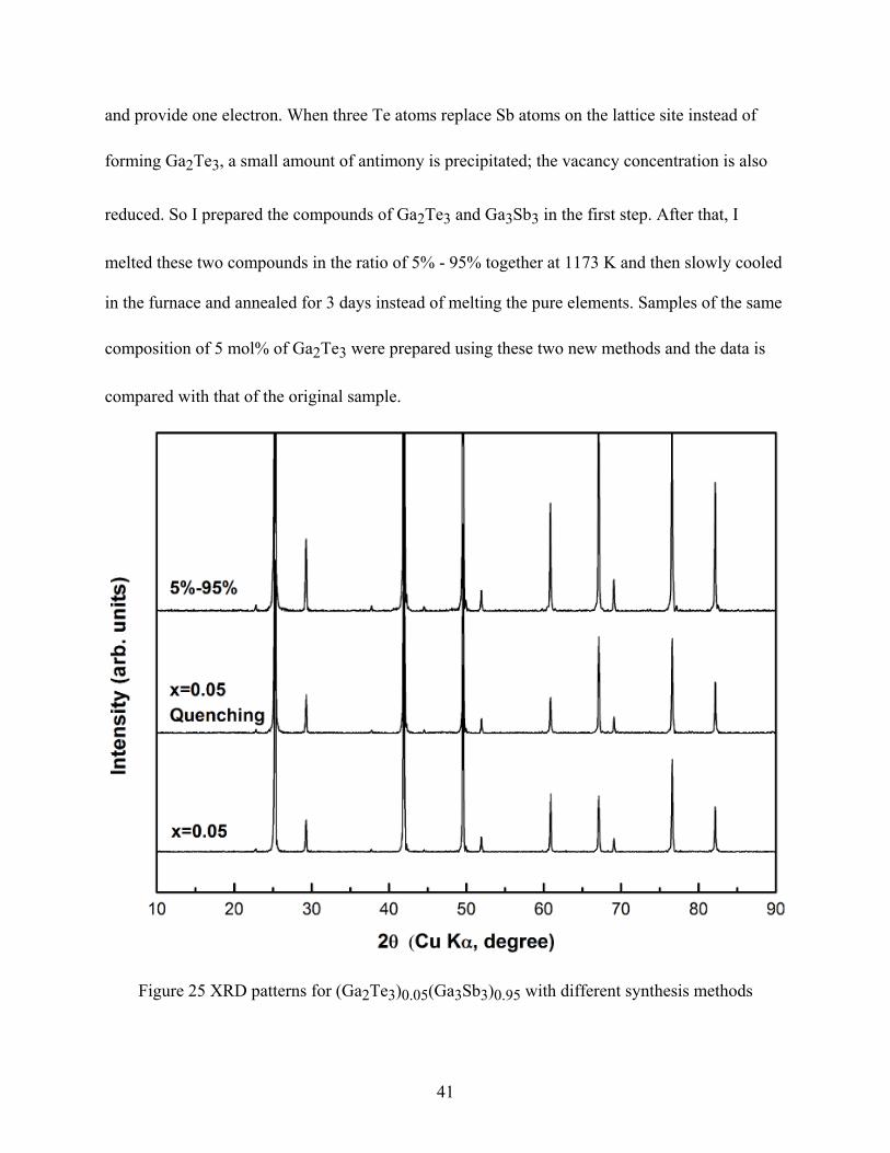
Figure 25 XRD patterns for (Ga2Te3)0.05(Ga3Sb3)0.95 with different synthesis methods
41
From Figure 25, all the three samples with different synthesis methods possess the zinc-
blende structure with same lattice constant. The data of lattice thermal conductivity is plotted in
Figure 26. The two samples with new synthesis methods possess lower κL. The reduction of κL
of the quenched sample is due to the decreased grain size and increased effect of grain boundary
scattering of phonons. The quenching process can help to prevent the impurity phase during
solidification which leads to higher Ga2Te3 and vacancy concentration that decrease the lattice
thermal conductivity. Additionally, it is possible that an ordered vacancy state could be formed
by quenching, as is reported by Chang-eun Kim32, which can scatter phonons more effectively.
The sample prepared by melting 5 mol% Ga2Te3 and 95 mol% Ga3Sb3 possesses even lower
lattice thermal conductivity which is caused by the reduced number of Te atoms replacing Sb
atoms and increased vacancy concentration. But the resistivity for the new samples increase
compared to the original one. Especially for the sample of 5% - 95%, the resistivity is increased
by ten times as is shown in Figure 27.
42

Figure 26 Temperature dependence of lattice thermal conductivity of (Ga2Te3)0.05(Ga3Sb3)0.95 with different synthesis methods
Figure 27 Temperature dependence of resistivity of (Ga2Te3)0.05(Ga3Sb3)0.95 with different synthesis methods
The reason for the increased resistivity for new samples is the reduced carrier concentration
and mobility as is shown by Figure 28 and 29. The electron concentration of the quenched
sample is half of the original one which indicates less replacing Te atoms and more vacancies.
43

Vacancy can scatter phonons as well as electrons which leads to low mobility. But the mobility
of quenched sample is close to the original one which might be due to the occurrence of an
ordered state of vacancy. The ordered state will decrease the number of scattering centers in the
lattice thus to increase the mobility. The sample of 5% - 95% has even lower electron
concentration. With increased concentration, vacancies scatter phonons greatly that leads to the
very small mobility compared to the original sample. There is not much difference of Seebeck
coefficient between the quenched sample and the original one, but the sample of 5% - 95% has a
fairly large value of S as can be seen from Figure 30. From equation 10, the reduced Fermi
energy is -1.06 for the 5% - 95% sample, which is much smaller than that of the original sample
(0.14). The new synthesis method of melting the compounds of Ga2Te3 and GaSb reduces the
Fermi level which is consistent with decreased carrier concentration.
Figure 28 Temperature dependence of carrier concentration
44

Figure 29 Temperature dependence of mobility
Figure 30 Temperature dependence of Seebeck coefficient of (Ga2Te3)0.05(Ga3Sb3)0.95 with different synthesis methods
From Figure 31, the power factor of the new samples is reduced because of the increased
resistivity. Although the new methods reduce the number of Te atoms replacing Sb and increase
the vacancy concentration thus to further decrease the thermal conductivity, the lower carrier
45

concentration and mobility strongly suppresses the figure of merit, as is shown in Figure 32.
Increasing the amount of vacancy can reduce the thermal conductivity, but taking into account of
the carrier concentration and mobility, we need to control the vacancy concentration in a
reasonable range to achieve higher ZT value.
Figure 31 Temperature dependence of power factor of (Ga2Te3)0.05(Ga3Sb3)0.95 with different synthesis methods
Figure 32 Temperature dependence of figure of merit of (Ga2Te3)0.05(Ga3Sb3)0.95 with different synthesis methods
46

CHAPTER 3 Effect of doping on thermoelectric properties of Ga2Te3 – GaSb
In order to optimize the electronic property of this solid solution, the effect of p-type
doping and isoelectronic substitution of Ga2Te3 – GaSb is studied.
3.1 Thermoelectric property of Zinc-doped sample
Both of the compounds of GaSb and Ga2Te3 are p-type semiconductors, but the solid
solution with content of Ga2Te3 varying from 1% to 15% is n-type. The addition of Ga2Te3
greatly decreases thermal conductivity, and the Seebeck coefficient of this solid solution is quite
large which is around -200 μV/K at room temperature, but the large resistivity caused by low
carrier concentration reduces the figure of merit. When the content of Ga2Te3 is 7%, the room
temperature data of resistivity and carrier concentration is 0.015 Ωcm and 1.2×1018 cm-3.
Because Zn has one less valence electron then Ga, the replacing of Ga by Zn will increase the
hole concentration. So we tried p-type doping of zinc on Ga site to change the electronic
properties so as to achieve better thermoelectric performance.
We studied the effect of doping of the solid solution with 4 mol% of Ga2Te3 which
possesses the highest figure of merit. The samples in the composition of
(ZnxGa1-x)2.96Sb2.88Te0.12 (x=0, 1%, 2%, 5%, 10%) are prepared by the same vacuum melting
method as is stated above. From Figure 33, we can see that all the samples possess zinc-blende
structure. For the sample with 10% Zn, the second phase of Sb is detected as is pointed out by
the black arrow. Figure 34 shows the lattice constant of samples with different content of Zn.
The bending of the line at 5% and 10% of Zn indicates the limit solubility and that not all the Zn
47

atoms replace Ga atoms in the lattice. For the samples with 5% and 10% of Zn, some impurity
phases might be formed. Because the compound of ZnTe also crystallizes in zinc-blende
structure, it is hard detect in the XRD pattern. The thermal conductivity of these samples
increases with increasing amount of Zn which will be discussed in detail later. It is consistent
with the fact that ZnTe has large thermal conductivity (about 0.18 W/cmK at room
temperature38). Because it takes one more Zn atom to form the compound of Zn3Te3 than
Zn2Te3, when more ZnTe is formed, there will be not enough Zn atoms to balance the Sb atoms
which results in the precipitated Sb. This agrees with the second phase of Sb in 10% Zn sample
shown by Figure 33. So it is possible that ZnTe is formed in the samples.
Figure 33 XRD patterns of the zinc-doped samples
48

Figure 34 Dependence of lattice constant of zinc-doped samples on content of Zn
As is shown by Figure 35, the lattice thermal conductivity is always increasing with
increasing amount of Zn. This might be due to the formation of ZnTe which possesses large
thermal conductivity. With increasing amount of ZnTe, less Ga2Te3 and Zn2Te3 is formed which
results in the lower vacancy concentration. The reduced effect of phonon scattering by vacancy
will also cause the lattice thermal conductivity to increase.
Figure 35 Temperature dependence of lattice thermal conductivity of zinc-doped samples
49

The solid solution without Zn is n-type semiconductor. After doping, it turns to be p-type.
As is shown in Figure 36, for the sample with 1% Zn, the Seebeck coefficient changes its sign at
certain temperature. For the samples with 5% and 10% of Zn, the Seebeck coefficient is
relatively low which is due to the increased carrier concentration.
Figure 36 Temperature dependence of Seebeck coefficient of zinc-doped samples
The doping of Zn increases the hole concentration greatly, as is shown in Figure 37. But
from Figure 38, we can see that the doping of Zn also decreases the mobility by more than one
order of magnitude. As mentioned earlier, it is quite typical for the hole mobility to be smaller
than that of electron. Additionally, it is expected that there will by strong ionized impurity
scattering by Zn ions.
50

Figure 37 Temperature dependence of carrier concentration of zinc-doped samples
Figure 38 Temperature dependence of mobility of zinc-doped samples
The temperature dependence of resistivity is shown in Figure 39. Because of the greatly
reduced mobility, the resistivity of 1% and 2% Zn sample is increased. Especially for the sample
with 1% Zn, the resistivity is huge. The samples with 5% and 10% Zn have very small resistivity
which is due to the large carrier concentration.
51

Figure 39 Temperature dependence of resistivity of zinc-doped samples
Figure 40 Temperature dependence of figure of merit of zinc-doped samples
Figure of merit for the samples with different content of Zn is plotted in Figure 40. The ZT
value of the zinc-doped sample is decreased compared to the sample without doping. The doping
of zinc changes the solid solution to p-type semiconductor. At small amount of Zn, the resistivity
is increased greatly which is due to the reduced mobility by ionized impurity scattering of
electrons. At higher amount of Zn (5% and 10%), the resistivity is reduced, but the doping of Zn
alters the band structure and Fermi level which affects Seebeck coefficient. The addition of Zn
52

also helps to form second phase, such as ZnTe, which affects the formation of vacancy structure.
The doping of Zn altered the carrier type and electronic properties, but the negative effect on
mobility, Seebeck coefficient and thermal conductivity limits its thermoelectric performance.
3.2 Effect of isoelectronic substitution on thermoelectric properties
The doping of Zinc introduces ionized impurity into the solid solution and reduces the
mobility greatly which results in increased resistivity. Because of the small mass and atomic size
difference between Zn and Ga, the replacing of Ga by Zn cannot help to scatter phonons
effectively to reduce thermal conductivity. So we studied the effect of isoelectronic substitution
of indium on Ga site. Because Ga and In are in the same column of the periodic table and have
equal valence electrons, the replacing of Ga by In will not reduce mobility due to ionized
impurity scattering, and the mass and atomic size difference between Ga and In will increase the
phonon scattering effect to decrease thermal conductivity.
53

Figure 41 XRD patterns of samples with indium substitution
We substituted In into the solid solution with 4 mol% Ga2Te3 which possesses the highest
figure of merit. The samples in the composition of (InxGa1-x)2.96Sb2.88Te0.12 (x=0, 5%, 10%,
15%) are prepared by vacuum melting method and XRD patterns are plotted in Figure 41. As is
reported by Garandet39, InSb and GaSb can form complete solid solution. From Figure 41, the
sample with 5% In possesses the single phase of zinc-blende structure. But for the samples with
10% and 15% In, a second phase, as is indicated by black arrows, is detected to be in the
composition of (In0.2Ga0.8)Sb. The stoichiometric deviation of the second phase from the main
54

phase is caused by segregation during cooling process. As is seen from Figure 42, the lattice
constant of 10% and 15% In sample is smaller than expected value (dashed line) calculated from
Vegard’s Law. The smaller lattice constant indicates the lower In concentration than the
stoichiometric composition which is caused by the formation of the In-rich second phase.
Figure 42 Dependence of lattice constant on content of indium
In has heavier mass and larger atomic size than Ga, so we should expect the reduced
thermal conductivity due to point defect phonon scattering. From Figure 43, the lattice thermal
conductivity is decreased with increasing In, especially at high temperature.
55

Figure 43 Temperature dependence of lattice thermal conductivity of samples with indium substitution
InSb and In2Te3 are both n-type semiconductors, so the doping of In will not change the
carrier type of the solid solution. As is shown in Figure 44, the Seebeck coefficient for the
samples with different In content are almost the same. And from equation 10, the Seebeck
coefficient for partial degenerate semiconductor is only controlled by scattering parameter and
Fermi energy which means that the position of Fermi level for all the samples are the same.
Figure 44 Temperature dependence of Seebeck coefficient of samples with indium substitution
56

Since InSb has small effective mass which is about 0.014 m0, the substitution of In will
decrease the effective mass of the solid solution. From equation 8, the carrier concentration for
partial degenerate semiconductor is related to Fermi level and effective mass. Although the
Fermi energy for all the samples are the same, the reduced effective mass will decrease the
carrier concentration of In-substituted sample which is consistent with the data of carrier
concentration as is shown in Figure 45.
Figure 45 Temperature dependence of carrier concentration of samples with indium substitution
Because doping of In will not introduce ionized impurities, the mobility is not decreased
significantly. So, unlike the Zn-doped sample, the resistivity, as is shown in Figure 46, is
increased but still of the same order of magnitude as the sample without indium.
57

Figure 46 Temperature dependence of resistivity of samples with indium substitution
From Figure 47, the power factor of the In-substituted sample is decreased which is mainly
due to the lowered carrier concentration. The figure of merit is plotted in Figure 48. The thermal
conductivity of the In-doped sample is slightly decreased, but the small effective mass which
results in the reduced carrier concentration and electrical conductivity decreases the ZT value.
Figure 47 Temperature dependence of power factor of samples with indium substitution
58

Figure 48 Temperature dependence of figure of merit of samples with indium substitution
The sample with 10% and 15% of In contains second phase which is formed by segregation
in the slow cooling process. An attempt was made to quench the sample from the liquid state, but
this did not remove the impurity phase. The In-rich second phase is difficult to remove which
might be due to the flat liquidus line in phase diagram of InSb-GaSb. The addition of In lowers
thermal conductivity because of increased phonon scattering by point defect, but the small
effective mass of InSb which results in the reduced power factor cannot help to improve its
thermoelectric properties.
59

CHAPTER 4 Conclusion
The vacancy structure on Ga sub-lattice greatly decreases lattice thermal conductivity of
Ga2Te3 – GaSb. The reduction at both 80K and 300K is over one order of magnitude. Addition
of Ga2Te3 changes carrier type, increases electron concentration and lifts Fermi level of these
solid solutions. And wider band gap of GaSb makes it easier to control electronic properties by
doping. But with large amount of Ga2Te3 and high vacancy concentration, the reduction of
lattice thermal conductivity is limited and mobility is reduced due to point defect scattering of
phonons. So the value of μ/κL is lowered. Large amount of Ga2Te3 also reduces Fermi level
resulting in decreased carrier concentration. So we need to control the amount of Ga2Te3 to
achieve higher figure of merit. The optimized content of Ga2Te3 is 4 mol%.
Extrinsic doping of zinc introduces ionized impurity which reduces the mobility
significantly. In Zn-doped samples, a second phase of ZnTe is formed which lowers vacancy
concentration and increases lattice thermal conductivity. The vacancy structure is very sensitive
to composition and the formation of impurity phase will affects the vacancy concentration. In
indium substituted samples, the reduction of lattice thermal conductivity is smaller than that of
Ga2Te3 – GaSb, which indicates that vacancy structure can scatter phonons more effectively
than In substitution. Because of the large effective mass of GaSb, the sample without In
substitution which possesses larger effective mass has higher carrier concentration and power
factor.
60

Prospective research will involve measurement of high temperature thermoelectric
properties of Ga2Te3 – GaSb. The thermoelectric performance of other vacancy compounds, for
example Ga2Te3 – ZnTe, will also be investigated in the future.
61

BIBLIOGRAPHY
62

BIBLIOGRAPHY
[1] Irving B. Cadoff, Thermoelectric Materials and Devices (1960)
[2] Jingfeng Li, Introduction to New Materials for Information and Energy (Power Point)
[3] Paul H. Egli, Thermoelectricity (1958)
[4] Donald T. Morelli, Materials for Energy Applications (Power Point)
[5] H. J. Goldsmid, Applications of Thermoelectricity (1960)
[6] Yanzhong Pei, Applied Physics Letters 94, 122112 (2009)
[7] D.M. Rowe, CRC Handbook of Thermoelectrics (1995)
[8] G. Jeffrey Snyder, Nature Materials 7,105 (2008)
[9] S. Latturner, Journal of Solid State Chemistry 151, 61 (2000)
[10] B. Abeles, Phys. Rev. 131, 1906 (1963)
[11] J.L. Cui, Materials Science and Engineering B 135, 44 (2006)
[12] J. Callaway, Phys. Rev. 120, 1149 (1960)
[13] P.G. Klemens, Proc. Phys. Soc., London, Sect. A 68, 1113 (1955)
[14] D.L. Rode, Physics Review B 3, Number 10 3287 (1971)
[15] J.C. Woolley, J. Phys. Chem. Solids. 16, 138 (1960)
[16] J.C. Woolley, Proc. Phys. Soc. London 72, 867 (1958)
[17] Shigeo Yamaguchi, Applied Physics Letters 87, 201902 (2005)
[18] J.C. Woolley, Journal of the Electrochemical Society 113, 465 (1966)
[19] J.C. Woolley, Journal of the Electrochemical Society 111,951 (1964)
[20] Ken Kurosaki, Applied Physics Letters 93, 012101 (2008)
[21] E. Finkman, Phys. Rev. Letts. 31, 890 (1973)
[22] J. C. Woolley, Journal of the Electrochemical Society 108, 874 (1961)
63

[23] H.V. Wensierski, Solid State Ionics 101-103, 479 (1997)
[24] D.B. Gasson, Proceedings of the International Conference on Semiconductor Physics (Prague), 1032 (1960)
[25] P.M. Spencer, Brit. J. Appl. Phys. 15, 625 (1964)
[26] D.A. Wright, Brit. J. Appl. Phys. 1, 831 (1968)
[27] J.E. Lewis, Brit. J. Appl. Phys. 17, 783 (1966)
[28] J. O. Sofo, Physical Review B 49, Number 7 4565 (1994)
[29] J.C. Woolley, J. Phys. Chem. Solids. 16, 102 (1960)
[30] S.K. Patapis, J. Phys. Chem. Solids. 44, 851 (1983)
[31] S. Yamanaka, Journal of Electronic Materials 38, 1392 (2009)
[32] C. Kim, Phys. Status Solidi RRL 3, 221 (2009)
[33] M. Guymont, Philosophical Magazine A 66, 133 (1992)
[34] A. A. Abdurakhmanova, phys. stat. sol. 20, 777 (1967)
[35] A. A. Abdurakhmanova, phys. stat. sol. 17, 375 (1966)
[36] Jiaolin Cui, Journal of Applied Physics 105, 063703 (2009)
[37] P. Damayanthi, Journal of Applied Physics 86, 5060 (1999)
[38] G. A. Slack, Physical Review B 6, 3791 (1972)
[39] J. P. Garandet, Journal of Crystal Growth 106, 426 (1990)
64