thermal stabilization of a microring modulator using feedback control€¦ · thermal stabilization...
TRANSCRIPT

Thermal stabilization of a microring modulator using feedback control
Kishore Padmaraju,1,* Johnnie Chan,1 Long Chen,2 Michal Lipson,2,3 and Keren Bergman1
1Department of Electrical Engineering, Columbia University, 500 West 120th Street, New York, New York, USA 2School of Electrical and Computer Engineering, Cornell University, 428 Phillips Hall, Ithaca, New York, USA
3Kavli Institute at Cornell, Ithaca, New York, USA *[email protected]
Abstract: We describe and demonstrate the use of a feedback control system to thermally stabilize a silicon microring modulator subjected to a thermally volatile environment. Furthermore, we establish power monitoring as an effective and appropriate mechanism to infer the temperature drift of a microring modulator. Our demonstration shows that a high-performance silicon microring-based device, normally inoperable in thermally volatile environments, can maintain error-free performance when a feedback control system is implemented.
©2012 Optical Society of America
OCIS codes: (230.4110) Modulators; (230.4555) Coupled resonators; (200.4650) Optical interconnects.
References and links
1. Q. Xu, B. Schmidt, S. Pradhan, and M. Lipson, “Micrometre-scale silicon electro-optic modulator,” Nature 435(7040), 325–327 (2005).
2. B. E. Little, J. S. Foresi, G. Steinmeyer, E. R. Thoen, S. T. Chu, H. A. Haus, E. P. Ippen, L. C. Kimerling, and W. Greene, “Ultra-compact Si/SiO2 microring resonator optical channel dropping filters,” IEEE Photon. Technol. Lett. 10(4), 549–551 (1998).
3. H. L. R. Lira, S. Manipatruni, and M. Lipson, “Broadband hitless silicon electro-optic switch for on-chip optical networks,” Opt. Express 17(25), 22271–22280 (2009).
4. F. Xia, L. Sekaric, and Y. A. Vlasov, “Ultra-compact optical buffers on a silicon chip,” Nat. Photonics 1(1), 65–71 (2007).
5. K. Preston, Y. H. D. Lee, M. Zhang, and M. Lipson, “Waveguide-integrated telecom-wavelength photodiode in deposited silicon,” Opt. Lett. 36(1), 52–54 (2011).
6. A. Shacham, K. Bergman, and L. P. Carloni, “Photonic networks-on-chip for future generations of chip multiprocessors,” IEEE Trans. Comput. 57(9), 1246–1260 (2008).
7. C. Batten, A. Joshi, J. Orcutt, A. Khilo, B. Moss, C. Holzwarth, M. Popovic, H. Li, H. Smith, J. Hoyt, F. Kaertner, R. Ram, V. Stojanovic, and K. Asanovic, “Building manycore processor to DRAM networks with monolithic silicon photonics,” IEEE Symposium on High-Performance Interconnects, 21–30 (2008).
8. Y. P. Varshni, “Temperature dependence of the energy gap in semiconductors,” Physica (Amsterdam) 34(1), 149–154 (1967).
9. M. S. Nawrocka, T. Liu, X. Wang, and R. R. Panepucci, “Tunable silicon microring resonator with wide free spectral range,” Appl. Phys. Lett. 89(7), 071110 (2006).
10. K. Padmaraju, J. Chan, L. Chen, M. Lipson, and K. Bergman, “Dynamic Stabilization of a Microring Modulator Under Thermal Perturbation,” Proc. Optical Fiber Communication Conference (Optical Society of America, 2012), paper OW4F.2.
11. B. Guha, K. Preston, and M. Lipson, “Athermal silicon microring electro-optic modulator,” Opt. Lett. 37(12), 2253–2255 (2012).
12. J. Teng, P. Dumon, W. Bogaerts, H. Zhang, X. Jian, X. Han, M. Zhao, G. Morthier, and R. Baets, “Athermal Silicon-on-insulator ring resonators by overlaying a polymer cladding on narrowed waveguides,” Opt. Express 17(17), 14627–14633 (2009).
13. C. T. DeRose, M. R. Watts, D. C. Trotter, D. L. Luck, G. N. Nielson, and R. W. Young, “Silicon microring modulator with integrated heater and temperature sensor for thermal control,” Proc. Conference on Lasers and Electro-Optics (Optical Society of America, 2010), paper CThJ3.
14. C. Qiu, J. Shu, Z. Li, X. Zhang, and Q. Xu, “Wavelength tracking with thermally controlled silicon resonators,” Opt. Express 19(6), 5143–5148 (2011).
#176247 - $15.00 USD Received 14 Sep 2012; revised 7 Nov 2012; accepted 7 Nov 2012; published 3 Dec 2012(C) 2012 OSA 17 December 2012 / Vol. 20, No. 27 / OPTICS EXPRESS 27999

15. A. L. Lentine, W. A. Zortman, D. C. Trotter, and M. R. Watts, “Active wavelength control of silicon microphotonic resonant modulators,” Proc. Optical Interconnects Conference (IEEE, 2012), paper TuC5.
16. E. Timurdogan, A. Biberman, D. C. Trotter, and C. Sun, M. Moresco, V. Stojanovic, M. R. Watts, “Automated Wavelength Recovery for Microring Resonators,” Proc. Conference on Lasers and Electro-Optics (Optical Society of America, 2012), paper CM2M.1.
17. L. Chen, K. Preston, S. Manipatruni, and M. Lipson, “Integrated GHz silicon photonic interconnect with micrometer-scale modulators and detectors,” Opt. Express 17(17), 15248–15256 (2009).
18. M. S. Nawrocka, T. Liu, X. Wang, and R. R. Panepucci, “Tunable silicon microring resonator with wide free spectral range,” Appl. Phys. Lett. 89(7), 071110 (2006).
19. Q. Xu, S. Manipatruni, B. Schmidt, J. Shakya, and M. Lipson, “12.5 Gbit/s carrier-injection-based silicon micro-ring silicon modulators,” Opt. Express 15(2), 430–436 (2007).
20. S. Manipatruni, R. K. Dokania, B. Schmidt, N. Sherwood-Droz, C. B. Poitras, A. B. Apsel, and M. Lipson, “Wide temperature range operation of micrometer-scale silicon electro-optic modulators,” Opt. Lett. 33(19), 2185–2187 (2008).
21. G. Li, X. Zheng, J. Yao, H. Thacker, I. Shubin, Y. Luo, K. Raj, J. E. Cunningham, and A. V. Krishnamoorthy, “25Gb/s 1V-driving CMOS ring modulator with integrated thermal tuning,” Opt. Express 19(21), 20435–20443 (2011).
22. W. A. Zortman, A. L. Lentine, D. C. Trotter, and M. R. Watts, “Integrated CMOS Compatible Low Power 10Gbps Silicon Photonic Heater-Modulator,” Proc. Optical Fiber Communication Conference (Optical Society of America, 2012), paper OW4I.5.
23. D. F. Logan, P. Velha, M. Sorel, R. M. De La Rue, P. E. Jessop, and A. P. Knights, “Monitoring and Tuning Micro-ring Properties Using Defect-Enhanced Silicon Photodiodes at 1550 nm,” IEEE Photon. Technol. Lett. 24(4), 261–263 (2012).
24. M. W. Geis, S. J. Spector, M. E. Grein, J. U. Yoon, D. M. Lennon, and T. M. Lyszczarz, “Silicon waveguide infrared photodiodes with >35 GHz bandwidth and phototransistors with 50 AW-1 response,” Opt. Express 17(7), 5193–5204 (2009).
25. M. W. Geis, S. J. Spector, R. C. Williamson, and T. M. Lyszczarz, “Submicrosecond submilliwatt silicon-on-insulator thermooptic switch,” IEEE Photon. Technol. Lett. 16(11), 2514–2516 (2004).
26. H. Yu, Y. Shi, L. He, and T. Karnik, “Thermal Via Allocation for 3-D ICs Considering Temporally and Spatially Variant Thermal Power,” IEEE Trans.VLSI Systems 16(12), 1609–1619 (2008).
1. Introduction
Microring-based nanophotonic devices have the ability to resolve the bandwidth-density challenges facing future multi-core processors. The resonance characteristics of microrings can be utilized to create modulators, filters, switches, buffers and detectors that are ideal for wavelength-division-multiplexed (WDM) photonic links in future chip-scale interconnection networks [1–5]. Furthermore, the compact size of microring-based devices aid in reducing the physical footprint and energy consumption of the photonic layer, two important constraints that must be satisfied in order for photonics to be closely integrated with electronics. Utilizing these advantages, prior research has validated microring-based photonic interconnection networks for the purpose of alleviating bandwidth bottlenecks in current computing systems [6,7].
However, for the successful integration of photonics and electronics the thermal issues that plague nanophotonic devices must be resolved. Silicon microring-based devices are especially susceptible to thermal fluctuations due to the relatively high thermo-optic coefficient of silicon and the resonant nature of the microring [8,9]. The wavelength resonance of the microring, while advantageous for WDM operation, makes the optical functionality of the device vulnerable to shifts in the resonant wavelength induced by thermal fluctuations. Temperature changes as small as ~1 K are enough to significantly shift the operating wavelength of the microring, and thus render the device inoperable [10].
Past attempts to resolve the thermal sensitivity of passive and active microring-based devices have focused on creating thermally insensitive structures [11,12], integrated temperature monitoring structures [13], dynamic feedback systems [14,15], and wavelength recovery algorithms [16]. However, to date, none of these attempts have demonstrated error-free operation of an active microring-based device in a thermally volatile environment (e.g. an operational microelectronic system.)
In this work we establish a general methodology to thermally stabilize a microring modulator using a feedback control system. The scheme we implement requires a monitor for
#176247 - $15.00 USD Received 14 Sep 2012; revised 7 Nov 2012; accepted 7 Nov 2012; published 3 Dec 2012(C) 2012 OSA 17 December 2012 / Vol. 20, No. 27 / OPTICS EXPRESS 28000

observing temperature drift, a mechanism to adjust the temperature accordingly, and a feedback controller to maintain closed-loop operation of the system. Using the techniques of power-monitoring and bias tuning, we experimentally show that this general dynamic is sufficient to maintain the high data-rate performance of a silicon microring modulator under temperature conditions that would normally render it inoperable.
2. Feedback control mechanism
The active microring-based device in this demonstration is a silicon microring modulator capable of 10-Gb/s modulation, fabricated at the Cornell Nanofabrication Facility. As pictured in Fig. 1(a), the device consists of a 6-µm-radius microring side-coupled to a waveguide. The microring and waveguide are designed for quasi-TE mode using a width and height of 450 nm and 260 nm, respectively. A 50-nm Si slab surrounding the microring was doped accordingly to produce the PIN structure capable of injecting carriers into the microring, which is necessary to produce the high-speed resonance shift required for optical modulation. Further fabrication details can be found in [17].
The thermal sensitivity of the resonance is given by the relation Δλ = λ0(Δn/ΔT)/neff, where λ0 is the resonant wavelength, (Δn/ΔT) is the thermo-optic coefficient, and neff is the effective index [18]. The mode of the slab waveguide geometry is simulated and found to have an effective index of 2.52 for the quasi-TE mode at the wavelength of 1550 nm. The thermo-optic coefficient of silicon is 1.86 10−4 K−1, yielding a resonance shift of 0.11 nm/K for the microring.
Fig. 1. (a) Scanning-electron-microscope (SEM) image of the microring modulator. (b) Schematic outlining the testing and implementation of a feedback system for thermally stabilizing the microring modulator.
In Fig. 1(b) a general outline of the feedback system is presented. As aforementioned, the feedback system requires both the monitoring and adjusting of the temperature, implemented here using optical power monitoring and bias tuning, respectively. Additionally, for the purpose of testing and validating the feedback system, a method is required to generate temperature fluctuations at the microring modulator.
Localized Temperature Heating
The evaluation of our feedback system requires the ability to dynamically inflict temperature changes on the microring modulator, akin to what the modulator would experience in a thermally volatile microelectronics environment. A traditional experimental setup would utilize a thermo-electric cooler (TEC) to produce the desired effect. However, TECs can be limited in bandwidth, and more importantly, heating and cooling of the entire nanophotonic chip will result in expansion and contraction of the entire chip, and subsequently, optical decoupling when using lateral fiber coupling. To resolve these issues, for this experimental demonstration a high-power multistripe 647-nm visible laser was used to inflict thermal fluctuations on the microring modulator. As depicted in Fig. 2(a), a cleaved multi-mode fiber is shone vertically on the microring modulator. Transparent to silicon dioxide, the 647-nm
#176247 - $15.00 USD Received 14 Sep 2012; revised 7 Nov 2012; accepted 7 Nov 2012; published 3 Dec 2012(C) 2012 OSA 17 December 2012 / Vol. 20, No. 27 / OPTICS EXPRESS 28001

light is able to pass through the SiO2 cladding after which it is absorbed by the silicon layer in the localized region of the microring modulator.
Fig. 2. (a) Generation of thermal fluctuations using a visible laser. (b) Measured bandwidth of the thermal fluctuations produced by the visible laser.
Through internal sinusoidal modulation of the 647-nm laser, a thermal fluctuation is produced in the localized vicinity of the microring modulator. Because the thermal fluctuation is localized to the microring modulator, the coupling of optical power into the chip is not affected, thereby enabling the use of optical power monitoring. In future implemented systems, the power-monitoring photodiode can be integrated within the chip and the need for this specialized heating mechanism will not be necessary. However, for this initial experimental demonstration this technique provides the necessitated localized heating.
To characterize the bandwidth of this technique a CW-laser was coupled into the modulator chip while the modulator was in its passive state, and the laser wavelength was tuned to the modulator’s resonance (Fig. 2(a)). The 647-nm laser was modulated with a sinusoid, while the output of the chip was received on an appropriate photodiode. The modulation produced on the photodiode (from the thermal modulation of the resonance) was measured for frequencies up to 100 kHz (Fig. 2(b)). It was found that the thermal modulation has a bandwidth of 18 kHz. 18 kHz is the modulation bandwidth of the 647-nm laser used for the experiment, indicating that the visible laser technique is not bandwidth-limited in the tested frequency regime (5 kHz).
Power Monitoring
As part of the feedback system, a mechanism is needed to ascertain any temperature shift that the modulator experiences. This temperature shift can be either directly measured, by using a temperature sensor [13], or indirectly inferred by examining the data signal. The latter method has previously been implemented through comparative logic at the individual bit level [15]. While this technique is effective, the use of high-speed logic will have repercussions on the energy-efficiency of the feedback system. For this reason, we motivate the use of a power monitoring scheme to track temperature fluctuations at the microring modulator.
As Fig. 3(a) shows, the mean optical power is an average between the power in the one and zero bit-states of the modulation. At the position of ideal on-off-keyed (OOK) data generation (i.e. the extinction ratio is maximized) the mean optical power of the signal will be at a minimum. Subsequently, the mean optical power of the signal will rise if either the wavelength of the laser or the resonant wavelength of the microring deviates. We show this behavior through a measurement of the mean optical power of the generated data signal as the wavelength of the laser is swept (Fig. 3(b)). Eye diagrams of the 10-Gb/s optical signal are also recorded at incremental wavelengths, and are shown inset in Fig. 3(b). While this measurement was done by sweeping the wavelength, an identical result will be produced by sweeping the temperature, which has been charted on the top axis of Fig. 3(b). The red highlighted inset shows that the ideal OOK signal is generated when the mean optical power is at a minimum. The dashed red region of Fig. 3(b) indicates a region of wavelengths (or equivalent temperature deviation) where suitable OOK is generated for data transmission. This monotonically increasing slope can be used to detect changes in the temperature of the
#176247 - $15.00 USD Received 14 Sep 2012; revised 7 Nov 2012; accepted 7 Nov 2012; published 3 Dec 2012(C) 2012 OSA 17 December 2012 / Vol. 20, No. 27 / OPTICS EXPRESS 28002

microring modulator. Increases or decreases in the received optical power indicate corresponding decreases or increases, respectively, of the temperature at the modulator. To exploit this monotonically increasing slope for our feedback system the wavelength is aligned not to the minimum point (where ideal OOK is generated), but to a point on the middle of the slope. Our experimental results will show that not operating at the point of minimum mean power will result in only a minimal performance degradation of the generated OOK signal.
Fig. 3. (a) The mean optical power is given as half of the power between the two bit-states of the modulated resonance. (b) Measured mean optical power of the 10-Gb/s microring-modulated optical signal versus wavelength. Eye diagrams of the 10 Gb/s signal are incrementally shown at points on the wavelength scan. The top x-axis gives the equivalent range when sweeping the temperature.
Because this method requires only the mean power of the optical signal, the photodetector used to monitor the signal can have a much smaller bandwidth than the GHz-rate optical signal it is monitoring. Subsequently, this monitoring mechanism is more opportune to be energy-efficient because the bandwidth of the slow photodetector used can be matched to the bandwidth of the thermal fluctuations afflicting the microring modulator. Additionally, only a small tap of the optical power is required to ascertain the mean power of the signal, minimizing the insertion loss added by the monitoring system. Lastly, it should be noted that this method operates on the assumption that over a large data set, the ratio of ‘1’ bits to ‘0’ bits does not change. For instances where this may not be a necessarily safe assumption, encoding schemes such as 8b/10b can be use to guarantee a DC-balanced data stream.
Thermal Tuning
Once a deviation in temperature has been established, the temperature must be adjusted back to its normative value. In this experiment, this is performed by adjusting the bias voltage (and subsequently the current) of the electrical signal driving the microring modulator. In carrier-injection microring modulators a small forward bias current is necessary to attain optimum optical modulation [19]. Due to the significant amounts of heat generated by carrier recombination in the diode junction, the forward bias current has the ancillary effect of altering the temperature of the microring modulator. Hence, the bias current can be reduced or increased to cool or heat, respectively, the microring, thus counteracting thermal fluctuations in the ambient environment [20].
PID control
Closed-loop operation of a feedback system requires a feedback controller. In this demonstration, an analog proportional-integral-derivative (PID) controller was implemented. Because the signal coming off the power monitor is slow-speed, and subsequently the temperature adjustment is also slow-speed, the controller can be implemented using relatively slow-speed components. The slow-speed analog circuitry composing the feedback controller
#176247 - $15.00 USD Received 14 Sep 2012; revised 7 Nov 2012; accepted 7 Nov 2012; published 3 Dec 2012(C) 2012 OSA 17 December 2012 / Vol. 20, No. 27 / OPTICS EXPRESS 28003
consisted of op-amps with a bandwidth of 3 MHz and an instrumentation amplifier with a bandwidth of 20 MHz.
3. Experimental results
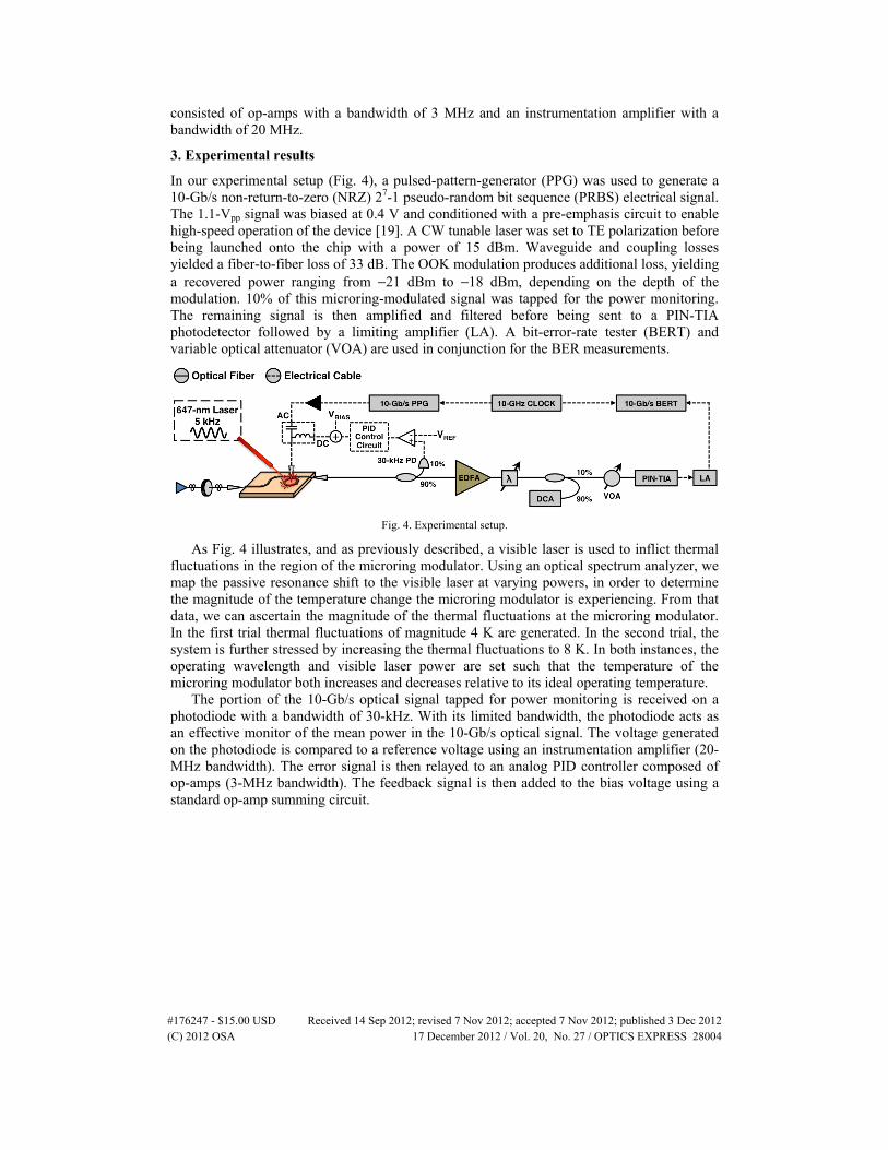
In our experimental setup (Fig. 4), a pulsed-pattern-generator (PPG) was used to generate a 10-Gb/s non-return-to-zero (NRZ) 27-1 pseudo-random bit sequence (PRBS) electrical signal. The 1.1-Vpp signal was biased at 0.4 V and conditioned with a pre-emphasis circuit to enable high-speed operation of the device [19]. A CW tunable laser was set to TE polarization before being launched onto the chip with a power of 15 dBm. Waveguide and coupling losses yielded a fiber-to-fiber loss of 33 dB. The OOK modulation produces additional loss, yielding a recovered power ranging from −21 dBm to −18 dBm, depending on the depth of the modulation. 10% of this microring-modulated signal was tapped for the power monitoring. The remaining signal is then amplified and filtered before being sent to a PIN-TIA photodetector followed by a limiting amplifier (LA). A bit-error-rate tester (BERT) and variable optical attenuator (VOA) are used in conjunction for the BER measurements.
Fig. 4. Experimental setup.
As Fig. 4 illustrates, and as previously described, a visible laser is used to inflict thermal fluctuations in the region of the microring modulator. Using an optical spectrum analyzer, we map the passive resonance shift to the visible laser at varying powers, in order to determine the magnitude of the temperature change the microring modulator is experiencing. From that data, we can ascertain the magnitude of the thermal fluctuations at the microring modulator. In the first trial thermal fluctuations of magnitude 4 K are generated. In the second trial, the system is further stressed by increasing the thermal fluctuations to 8 K. In both instances, the operating wavelength and visible laser power are set such that the temperature of the microring modulator both increases and decreases relative to its ideal operating temperature.
The portion of the 10-Gb/s optical signal tapped for power monitoring is received on a photodiode with a bandwidth of 30-kHz. With its limited bandwidth, the photodiode acts as an effective monitor of the mean power in the 10-Gb/s optical signal. The voltage generated on the photodiode is compared to a reference voltage using an instrumentation amplifier (20-MHz bandwidth). The error signal is then relayed to an analog PID controller composed of op-amps (3-MHz bandwidth). The feedback signal is then added to the bias voltage using a standard op-amp summing circuit.
#176247 - $15.00 USD Received 14 Sep 2012; revised 7 Nov 2012; accepted 7 Nov 2012; published 3 Dec 2012(C) 2012 OSA 17 December 2012 / Vol. 20, No. 27 / OPTICS EXPRESS 28004

Fig. 5. (a) The DC bias of the modulator, demonstrating how the feedback system dynamically adjusts the DC bias to counteract thermal fluctuations of magnitude 4 K and 8 K. (b) The voltage from the TIA following the photodiode (used to infer the mean modulation power) when the modulator is exposed to thermal fluctuations of magnitude 4 K, with and without the feedback system implemented. (c) The voltage on the TIA following the photodiode when the modulator is exposed to thermal fluctuations of magnitude 8 K, with and without the feedback system implemented.
The dynamic adjustment of the DC bias is illustrated in the oscilloscope trace of Fig. 5(a). Without the feedback circuit, the DC bias is set at a constant 0.4 V, whereas, with the feedback circuit, the voltage is swung dynamically to correct for the thermal fluctuations. Figure 5(a) shows the system when it is subjected to both 4-K and 8-K thermal fluctuations, with the DC bias swing larger (from 0.15 V to 0.50 V) for the latter scenario. The effect of this action can be seen in the voltage of the transimpedance-amplifier (TIA) following the photodiode (Fig. 5(b), 5(c)), which is an indication of the mean power in the 10-Gb/s optical signal. Without the feedback system the mean power fluctuates in correspondence with the thermal fluctuations. The feedback system locks the mean modulation power to the set reference, ensuring that the modulation is maintained throughout the duration of the thermal fluctuations.
The eye diagrams in Fig. 6 and bit-error-rate (BER) curves in Fig. 7 provide validation of the feedback system’s functionality. Figure 6(a) and 6(d) show eye diagrams of the microring-modulated optical signal when there are no thermal fluctuations, without and with the feedback system implemented, respectively. In this scenario, the eye diagrams show similar modulation performance, and furthermore, the measured BER curves of Fig. 7 show only a power penalty of 0.6 dB as a consequence of implementing the feedback system. This power penalty can be attributed to the operation of the microring modulator at a modulation point that, while optimal for the feedback system, is not optimal for the generation of optical data. It should be noted that the reference level was set to minimize this power penalty while ensuring that there was enough of a margin for the feedback system to operate successfully.
In Fig. 6(b) and Fig. 6(c) the eye diagram is shown for when the modulator is subjected to thermal fluctuations of 4 K and 8 K, respectively, and without the feedback system implemented. With thermal fluctuations of 4 K, the ensuing resonance shifts are severe enough that the data in the optical signal becomes severely distorted (Fig. 6(b)). When the thermal fluctuations are increased to 8 K, the distortion becomes further exacerbated, with the majority of the optical power contained at the ‘1’ level, as the modulator is shifted completely out of the modulation region for a significant portion of the thermal fluctuation (Fig. 6(c)). For both scenarios, the optical data is distorted to a degree that no BER measurement is possible.
#176247 - $15.00 USD Received 14 Sep 2012; revised 7 Nov 2012; accepted 7 Nov 2012; published 3 Dec 2012(C) 2012 OSA 17 December 2012 / Vol. 20, No. 27 / OPTICS EXPRESS 28005

Fig. 6. Eye diagrams of the 10-Gb/s microring modulation when subjected to temperature fluctuations of magnitude (a) 0 K (b) 4 K (c) and 8 K with no implemented feedback system. Similarly, eye diagrams of the 10-Gb/s microring modulation when subjected to temperature fluctuations of magnitude (d) 0 K (e) 4 K (f) and 8 K but with a feedback system thermally stabilizing the microring modulator.
In contrast, Fig. 6(e) and Fig. 6(f) show that with the implementation of the feedback system, the modulation of the microring modulator can be maintained, even when subjected to thermal fluctuations of 4 K and 8 K, respectively. BER measurements further validate this result with error-free performance, defined as a 10−12 error-rate, being measured when the feedback system is implemented (Fig. 7).
Fig. 7. Bit-error-rate (BER) measurements of the 10-Gb/s microring-modulated signal. These measurements correspond to the eye diagrams in Fig. 6(a), 6(d), 6(e), and 6(f).
Although the feedback system is able to maintain error-free performance in the presence of the aforementioned thermal fluctuations, there were power-penalties incurred as the
#176247 - $15.00 USD Received 14 Sep 2012; revised 7 Nov 2012; accepted 7 Nov 2012; published 3 Dec 2012(C) 2012 OSA 17 December 2012 / Vol. 20, No. 27 / OPTICS EXPRESS 28006

magnitude of the thermal fluctuations was increased. With thermal fluctuations of magnitude 4 K a power penalty of 0.4 dB is measured relative to the scenario with no thermal fluctuations (and with the feedback system implemented). When the thermal fluctuations are increased to a magnitude of 8 K this power penalty increases to 2.4 dB. These power penalties are evident in the eye diagrams of Fig. 6(e) and Fig. 6(f). As the magnitude of the thermal fluctuations increase the noise in the ‘1’ and ‘0’ levels also increase. This behavior is attributable to the DC biasing mechanism used for maintaining the temperature of the microring. The carrier dynamics of the microring modulator are sensitive to adjustments in the DC bias. As a result, even the small changes in DC bias caused by the feedback system produce distortions in the modulation of the microring modulator. As the thermal fluctuations increase in magnitude the feedback system responds by applying larger variations to the DC bias, incidentally producing more distortion in the modulation of the modulator, and an ensuing increase in power penalty.
4. Discussion and conclusion
We have described a methodology for the thermally stabilization of active microring modulators and experimentally implemented the feedback system on a 10-Gb/s silicon microring modulator in an environment of thermal volatility that would normally render the microring modulator inoperable. Our implemented system was shown to guarantee error-free performance up to the tested 5-kHz thermal fluctuation of 8 K.
This demonstration served as an effective proof-of-concept demonstration for the general type of feedback system we described. Further improvements can both improve and extend on the results reported in this paper. For example, while this demonstration was able to leverage the DC biasing mechanism of the microring modulator for the adjustment of the modulator temperature, future iterations of the system would benefit from the use of an integrated heater. Integrated heaters enable power-efficient temperature tuning over a much larger range than the DC biasing mechanism [21]. Error-free 10-Gb/s microring modulation has been demonstrated when tuning a silicon microring modulator across a range greater than 60 K, with no performance penalties resultant of the temperature tuning across the cited temperature range [22]. In contrast, the DC biasing mechanism alters the high-speed electrical signal driving the microring modulator and results in a degradation of the generated optical signal. In future implementations, using an integrated heater to adjust the temperature of the microring modulator will allow for a larger range of temperature fluctuations to be tolerated, with no inherent penalties in the performance of the modulator.
Future implementations will also benefit from an integration of the photodetector with the microring modulator. Due to the high coupling losses, we required a 10% tap of the optical signal to implement the power-monitoring mechanism. With an integrated photodetector, the tap can be reduced. For this purpose, the use of defect-enhanced silicon photodiodes may be ideal. With their low photoabsorption they can serve as effective in-waveguide monitors of the optical signal being generated by the microring modulator [23]. Furthermore, these photodetectors can be implemented on both the through and drop ports of the microring modulator, permitting a configuration whereby the feedback system would be able to make a relative reference against the optical power reaching the microring modulator [24]. This would give the feedback system immunity against changes in the amount of optical power reaching the modulator, which are primarily due to changes in the coupling loss or fluctuations in the laser power.
The integration of the component parts comprising the feedback system has the potential to improve both the power-efficiency of the system as well as improve the responsivity, that is, the bandwidth of the thermal fluctuations that the feedback system is able to counteract. In this demonstration the feedback system counteracted a thermal fluctuation of a single harmonic, but it has been previously been demonstrated that it can counteract thermal fluctuations of varying frequency [10]. In comparison to [10], in this demonstration we
#176247 - $15.00 USD Received 14 Sep 2012; revised 7 Nov 2012; accepted 7 Nov 2012; published 3 Dec 2012(C) 2012 OSA 17 December 2012 / Vol. 20, No. 27 / OPTICS EXPRESS 28007
extended the frequency of the thermal fluctuation to 5 kHz. Thermal time constants in silicon-on-insulator systems struggle to reach below the microsecond time-scale, indicating that the feedback system needs to only contend with thermal fluctuations in the sub-MHz regime [25]. More likely, in a microelectronics environment, where the thermal time constants are in the millisecond range, the bandwidth we have demonstrated is sufficient [26]. Regardless, the bandwidth of the feedback system can be extended or reduced as needed by extending or reducing the bandwidth of the component parts to the desired range. In this manner the bandwidth of the feedback system can be matched to the bandwidth of the thermal fluctuations it is counteracting, thereby optimizing the power-efficiency of the feedback system.
Acknowledgments
The authors gratefully acknowledge Richard Grote for the effective index calculation. This work was supported in part by the Interconnect Focus Center, one of five research centers funded under the Focus Center Research Program, a Semiconductor Research Corporation (SRC) and DARPA program, and by the National Science Foundation and SRC under grant ECCS-0903406 SRC Task 2001.
#176247 - $15.00 USD Received 14 Sep 2012; revised 7 Nov 2012; accepted 7 Nov 2012; published 3 Dec 2012(C) 2012 OSA 17 December 2012 / Vol. 20, No. 27 / OPTICS EXPRESS 28008