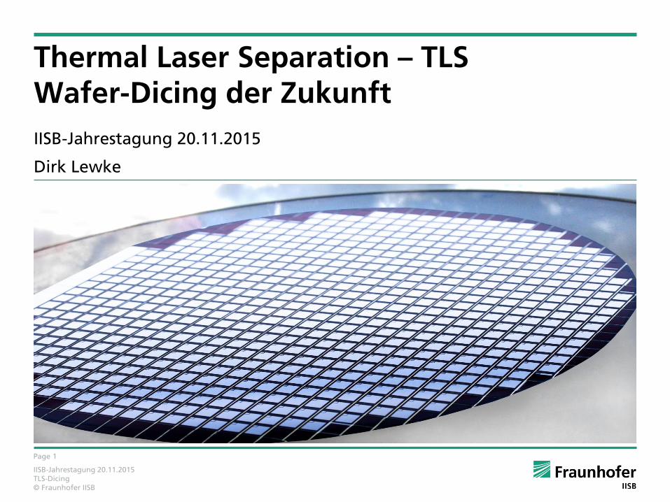
thermal laser separation tls wafer-dicing der zukunft · thermal laser separation – tls...
TRANSCRIPT
Page 1
IISB-Jahrestagung 20.11.2015 TLS-Dicing © Fraunhofer IISB
IISB-Jahrestagung 20.11.2015
Dirk Lewke
Thermal Laser Separation – TLS Wafer-Dicing der Zukunft
Page 2
IISB-Jahrestagung 20.11.2015 TLS-Dicing © Fraunhofer IISB
Agenda
- State of the art dicing technology in semiconductor industry
- Principle of Thermal Laser Separation
- Exemplary applications
- TLS for Silicon dicing
- TLS for SiC dicing

Page 3
IISB-Jahrestagung 20.11.2015 TLS-Dicing © Fraunhofer IISB
Principle:
fast rotating dicing blade is guided along the dicing street and separates the chips out of the wafer.
abrasive process (material loss)
water cooling is necessary
State of the art dicing techniques Mechanical blade dicing
Source: Disco
Source: Dohnke, et al.: Comparison of different novel chip separation methods for 4H-SiC; ECSCRM 2014

Page 4
IISB-Jahrestagung 20.11.2015 TLS-Dicing © Fraunhofer IISB
1. Step – Crack initiation
With a diamond tip or a short pulsed
ablation laser
Realization of a predetermined cleaving
point
2. Step – Cleaving
Laser-based heating, subsequent water
spray cooling
Mechanical stress field capable of
guiding a crack along a line to be
cleaved
Crack guiding with thermally induced mechanical stress
Crack
initiation
Thermal Laser Separation – TLS
Principle

Page 5
IISB-Jahrestagung 20.11.2015 TLS-Dicing © Fraunhofer IISB
Thermal Laser Separation – TLS
Properties and Benefits
Kerf free crack guiding
More chips per wafer possible
High edge quality
No chipping, no micro cracks
High bending strength
No delamination of backside metal
No tool wear
Low CoO
High feed rate
Typical 200 - 300 mm/s
Works for different materials
Si, mc-Si, SiC and Ge with one tool configuration
No frontside chipping No backside
chipping
BSM
Page 6
IISB-Jahrestagung 20.11.2015 TLS-Dicing © Fraunhofer IISB
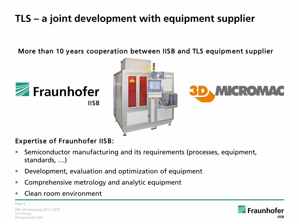
TLS – a joint development with equipment supplier
More than 10 years cooperation between IISB and TLS equipment supplier
Expertise of Fraunhofer IISB:
Semiconductor manufacturing and its requirements (processes, equipment, standards, …)
Development, evaluation and optimization of equipment
Comprehensive metrology and analytic equipment
Clean room environment
Page 7
IISB-Jahrestagung 20.11.2015 TLS-Dicing © Fraunhofer IISB
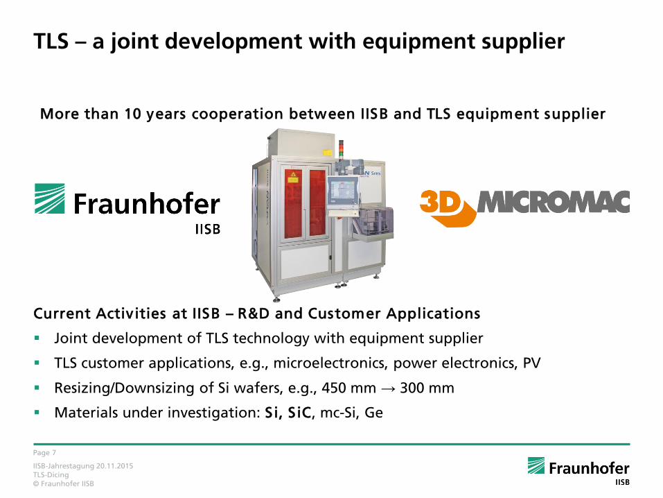
TLS – a joint development with equipment supplier
More than 10 years cooperation between IISB and TLS equipment supplier
Current Activ ities at IISB – R&D and Customer Applications
Joint development of TLS technology with equipment supplier
TLS customer applications, e.g., microelectronics, power electronics, PV
Resizing/Downsizing of Si wafers, e.g., 450 mm → 300 mm
Materials under investigation: S i, S iC, mc-Si, Ge
Page 8
IISB-Jahrestagung 20.11.2015 TLS-Dicing © Fraunhofer IISB
Agenda
- State of the art dicing technology in semiconductor industry
- Principle of Thermal Laser Separation
- Exemplary applications
- TLS for Silicon dicing
- TLS for SiC dicing
Page 9
IISB-Jahrestagung 20.11.2015 TLS-Dicing © Fraunhofer IISB
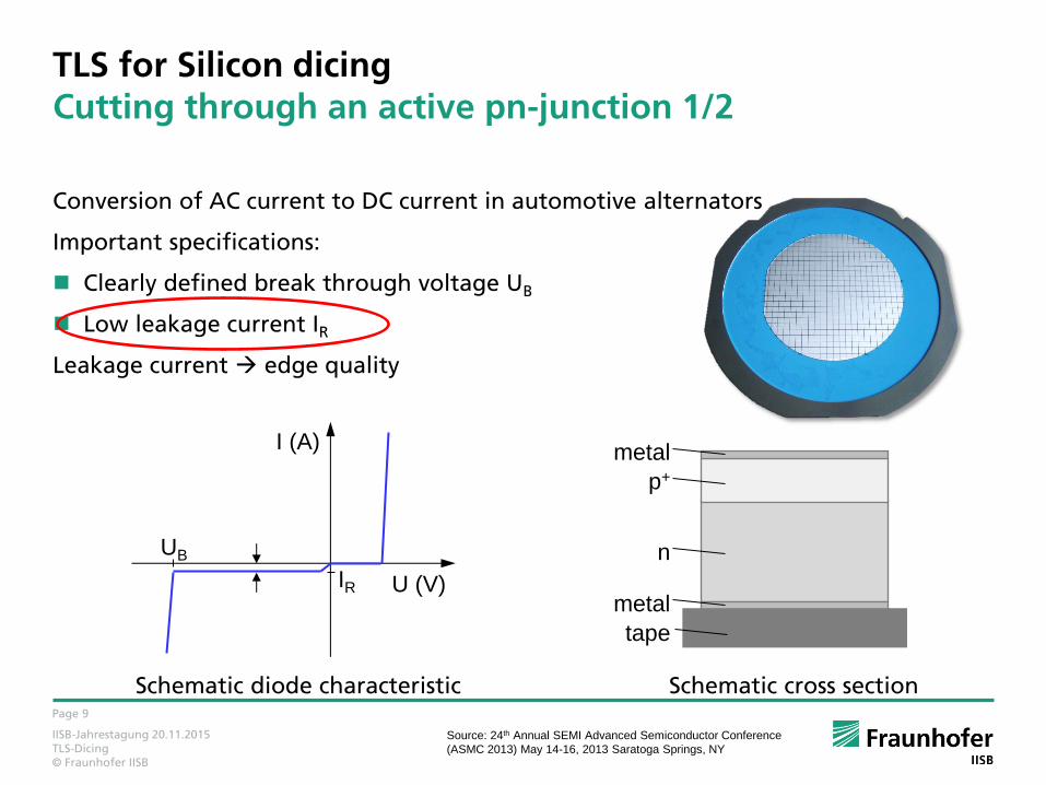
TLS for Silicon dicing Cutting through an active pn-junction 1/2
Conversion of AC current to DC current in automotive alternators
Important specifications:
Clearly defined break through voltage UB
Low leakage current IR
Leakage current edge quality
U (V)
I (A)
IR
UB
Schematic diode characteristic
metal
p+
n
metal
tape
Schematic cross section
Source: 24th Annual SEMI Advanced Semiconductor Conference
(ASMC 2013) May 14-16, 2013 Saratoga Springs, NY
Page 10
IISB-Jahrestagung 20.11.2015 TLS-Dicing © Fraunhofer IISB
Source: 24th Annual SEMI Advanced Semiconductor Conference
(ASMC 2013) May 14-16, 2013 Saratoga Springs, NY
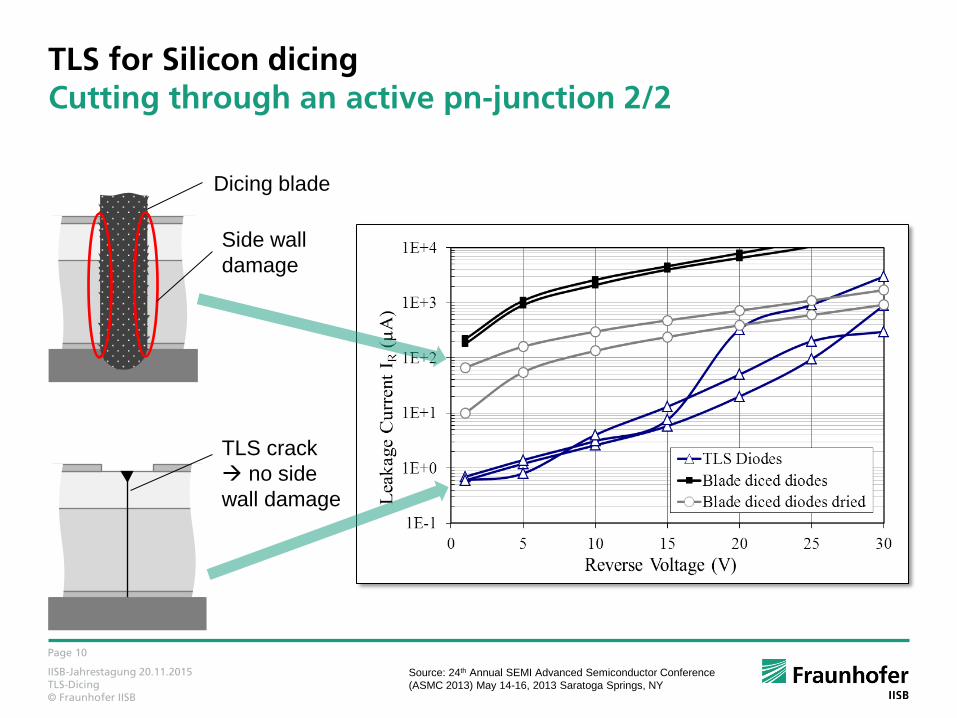
TLS for Silicon dicing Cutting through an active pn-junction 2/2
Dicing blade
TLS crack
no side
wall damage
Side wall
damage

Page 11
IISB-Jahrestagung 20.11.2015 TLS-Dicing © Fraunhofer IISB
Agenda
- State of the art dicing technology in semiconductor industry
- Principle of Thermal Laser Separation
- Exemplary applications
- TLS for Silicon dicing
- TLS for SiC dicing

Page 12
IISB-Jahrestagung 20.11.2015 TLS-Dicing © Fraunhofer IISB
TLS for SiC dicing Motivation
Due to the hardness of SiC – 9.2 on Mohs scale – dicing SiC is a “hard job”
0123456789
10
Hardness (Mohs)
Page 13
IISB-Jahrestagung 20.11.2015 TLS-Dicing © Fraunhofer IISB
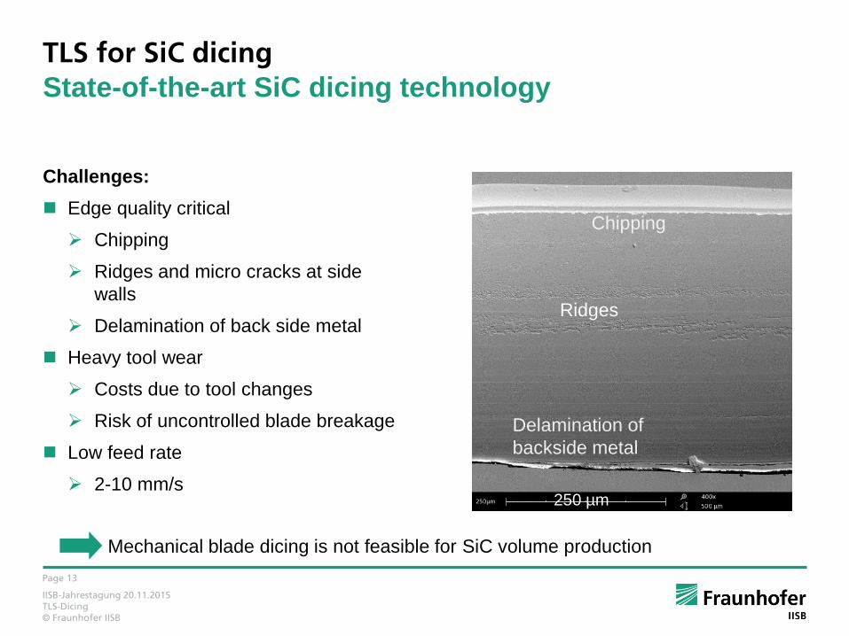
TLS for SiC dicing
State-of-the-art SiC dicing technology
Challenges:
Edge quality critical
Chipping
Ridges and micro cracks at side
walls
Delamination of back side metal
Heavy tool wear
Costs due to tool changes
Risk of uncontrolled blade breakage
Low feed rate
2-10 mm/s
Mechanical blade dicing is not feasible for SiC volume production
250 µm
Chipping
Delamination of
backside metal
Ridges
Page 14
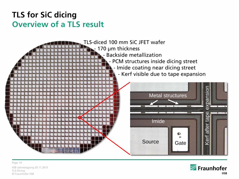
IISB-Jahrestagung 20.11.2015 TLS-Dicing © Fraunhofer IISB
Imide
Source Gate
Metal structures
Kerf
aft
er
tap
e e
xpansio
n
TLS for SiC dicing Overview of a TLS result
TLS-diced 100 mm SiC JFET wafer - 170 µm thickness - Backside metallization - PCM structures inside dicing street - Imide coating near dicing street - Kerf visible due to tape expansion

Page 15
IISB-Jahrestagung 20.11.2015 TLS-Dicing © Fraunhofer IISB
Assembly of TLS diced SiC diodes
TLS wafer dicing
Erlangen
Malaysia packaging
Germany
electrical characterization
Page 16
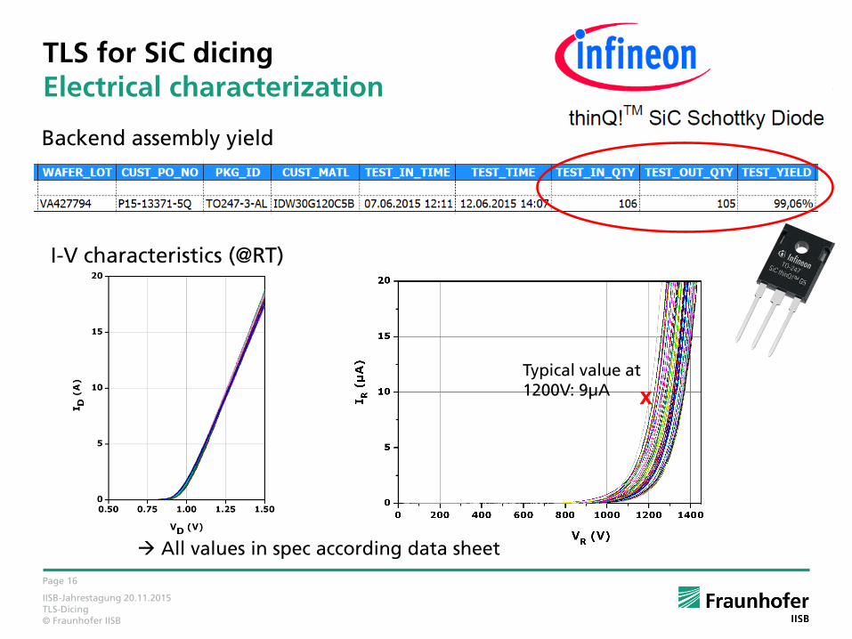
IISB-Jahrestagung 20.11.2015 TLS-Dicing © Fraunhofer IISB
Backend assembly yield
All values in spec according data sheet
I-V characteristics (@RT)
x Typical value at 1200V: 9µA
TLS for SiC dicing Electrical characterization
Page 17
IISB-Jahrestagung 20.11.2015 TLS-Dicing © Fraunhofer IISB
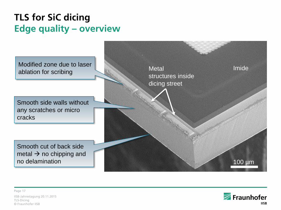
Imide Metal
structures inside
dicing street
100 µm
Modified zone due to laser
ablation for scribing
Smooth side walls without
any scratches or micro
cracks
Smooth cut of back side
metal no chipping and
no delamination
TLS for SiC dicing Edge quality – overview
Page 18
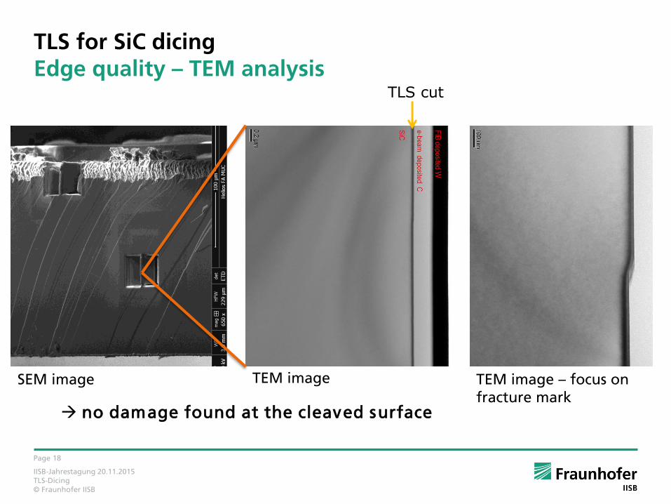
IISB-Jahrestagung 20.11.2015 TLS-Dicing © Fraunhofer IISB
no damage found at the cleaved surface
SEM image
TLS cut
TEM image TEM image – focus on fracture mark
TLS for SiC dicing Edge quality – TEM analysis
Page 19
IISB-Jahrestagung 20.11.2015 TLS-Dicing © Fraunhofer IISB
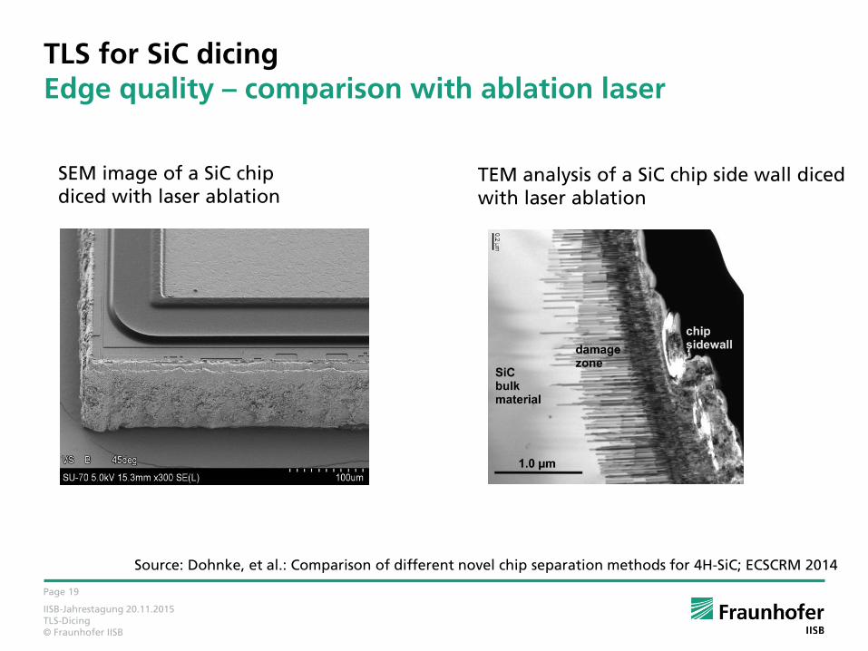
SEM image of a SiC chip diced with laser ablation
TEM analysis of a SiC chip side wall diced with laser ablation
Source: Dohnke, et al.: Comparison of different novel chip separation methods for 4H-SiC; ECSCRM 2014
TLS for SiC dicing Edge quality – comparison with ablation laser

Page 20
IISB-Jahrestagung 20.11.2015 TLS-Dicing © Fraunhofer IISB
Wafer: • 150 mm SiC • Back side metal • 160 µm thickness • 1 mm die edge length • PCM in street • 70 µm street width
Considered: • Consumables (saw blades) • Invest/depreciation for tool • Footprint
Process speed: • TLS: 200 mm/s • Mechanical blade dicing: 7 mm/s
TLS-Dicing™: 3.00 €
Mechanical blade dicing: 37.00 €
Blade dicer: 150 min per wafer microDICE™: 17 min per wafer
TLS for SiC dicing Cost calculations – Comparison with state-of-the-art
Page 21
IISB-Jahrestagung 20.11.2015 TLS-Dicing © Fraunhofer IISB
Summery and outlook
Summery
- TLS is a kerf free laser based dicing technology which is based on crack guiding using thermally induced mechanical stress.
- TLS has major benefits compared with state-of-the-art regarding:
- Edge quality
- Throughput
- Costs
- TLS works for different materials with same machine configuration
Outlook
- Improve the reliability and shift technological limits of the TLS process
- Investigate TLS for other materials like GaN
- Bring the TLS technology to industrial application
Page 22
IISB-Jahrestagung 20.11.2015 TLS-Dicing © Fraunhofer IISB
Thank you for your attention !
Contact:
Dirk Lewke
Fraunhofer IISB
Tel.: +49 9131 761-155