thermal dissipation in bonded structures - … dissipation in bonded structures rajiv v. joshi ,t....
TRANSCRIPT
Thermal Dissipation in Bonded Thermal Dissipation in Bonded StructuresStructures
Rajiv V. Joshi ,T. Smy1, K. Banerjee2, A. Topol
1University of Carleton, Ottawa, Canada2University of California, Santa Barbara, CA
IBM T. J. Watson Research CenterYorktown Heights, NY

R. V. Joshi (2)
OUTLINE• Introduction
• Real 3D structures
• Thermal impact on Circuit Performance
• Summary
• Multilayer Devices
• 3-D Thermal Modeling of Interconnects
3-D Thermal ModellingSelf heating in SOI
• Temperature Measurement Techniques
Oxide BondedCopper bonded

R. V. Joshi (3)
INTRODUCTION• Considerable interest in increasing on die device density by using wafer level 3D integration.
• One aspect of the new technologies that has to be addressed is the thermal impact of the front and backend technology.
• Some of the issues that need to be investigated are:
Self-heating effect on SOI wafersJoule heating in the backend (electrical resistance increaseswith T – nonlinear).Low-k materials (Thermal conductivity scales with k).Heat flow through the interconnect (complex geometry).Use of thermal vias and design rules to minimize temperature rises (optimization).
R. V. Joshi (4)
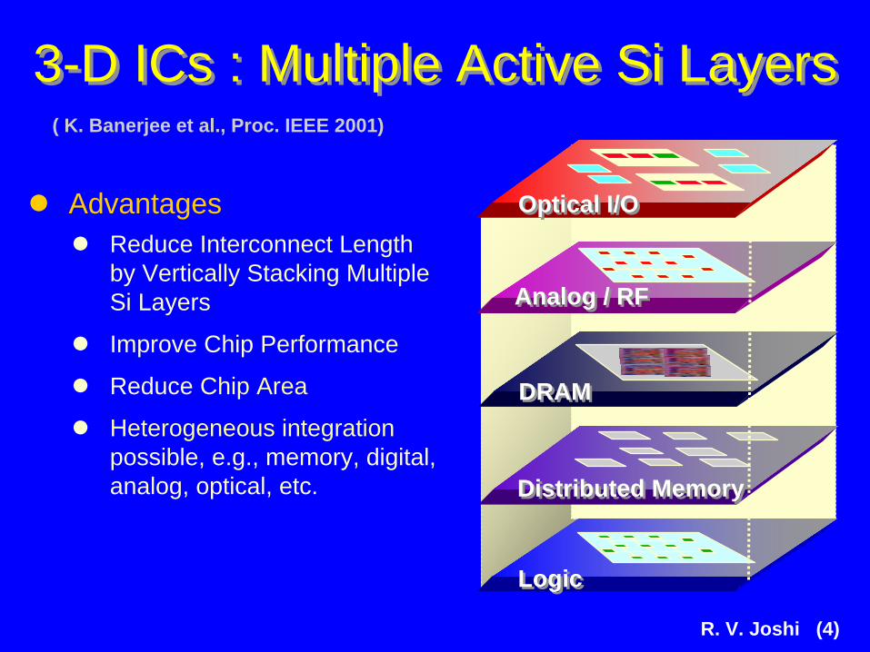
3-D ICs : Multiple Active Si Layers3-D ICs : Multiple Active Si Layers
AdvantagesReduce Interconnect Length by Vertically Stacking Multiple Si Layers
Improve Chip Performance
Reduce Chip Area
Heterogeneous integrationpossible, e.g., memory, digital, analog, optical, etc.
( K. Banerjee et al., Proc. IEEE 2001)
Logic Logic
Distributed MemoryDistributed Memory
DRAMDRAM
Analog / RFAnalog / RF
Optical I/OOptical I/O
R. V. Joshi (5)
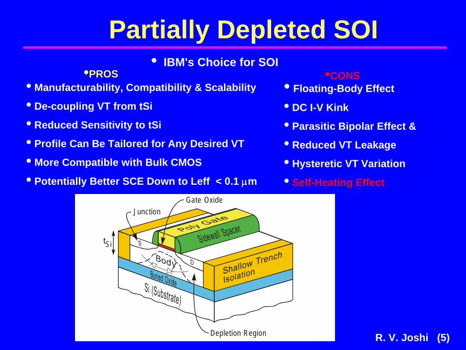
Partially Depleted SOI• IBM's Choice for SOI
• Manufacturability, Compatibility & Scalability
• De-coupling VT from tSi
• Reduced Sensitivity to tSi
• Profile Can Be Tailored for Any Desired VT
• More Compatible with Bulk CMOS
• Potentially Better SCE Down to Leff < 0.1 μm
• Floating-Body Effect
• DC I-V Kink
• Parasitic Bipolar Effect &
• Reduced VT Leakage
• Hysteretic VT Variation
• Self-Heating EffectGate Oxide
Depletion Region
Junction
tSi
•PROS •CONS
R. V. Joshi (6)
Self-Heating in SOI
• Self heating in SOI increases device junction temperature
• Modeled for single channel FET using 1-D thermal conduction model (Su et al)
• Analysis using 2-D heat conduction through SiO2 for simple single channel devices (Goodson et al.)
• Device geometries studied in the literature are not representative
of those typically used in high performance, large fan out circuits
R. V. Joshi (7)
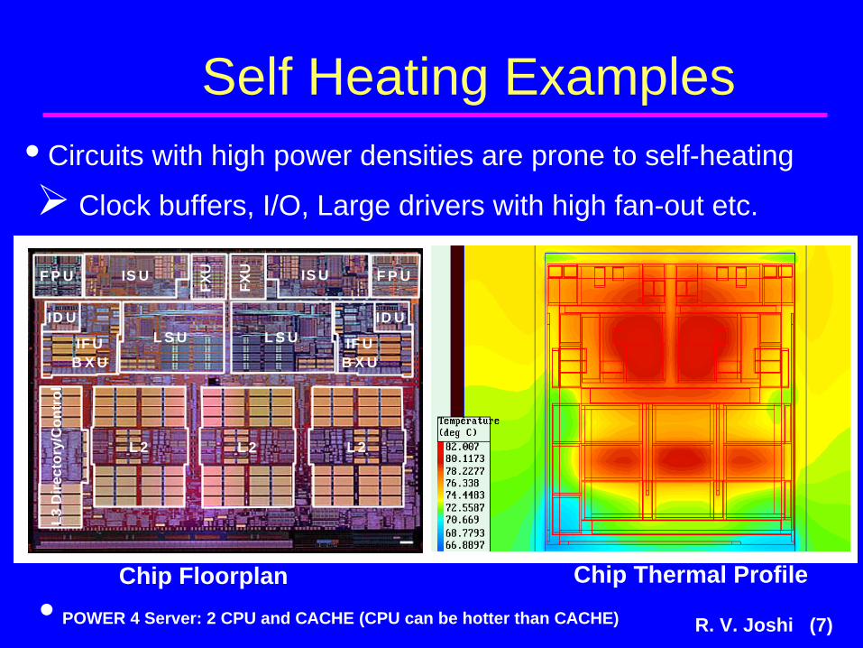
Self Heating Examples• Circuits with high power densities are prone to self-heating
Clock buffers, I/O, Large drivers with high fan-out etc.
L3 D
irect
ory/
Con
trol
L 2 L 2 L 2
L S U L S UIF UB X U
ID U ID U
IF UB X U
F P U F P U
FXU
FXUIS U IS U
Chip Floorplan Chip Thermal Profile• POWER 4 Server: 2 CPU and CACHE (CPU can be hotter than CACHE)

R. V. Joshi (8)
Circuits Used for AnalysisClock Tree
PFET
NFET
Output Buffers : NFET width - 2800μm NFET fingers - 280 PFET width - 5600μm PFET fingers - 280 Output load - 30pf (wire + device)
R. V. Joshi (9)
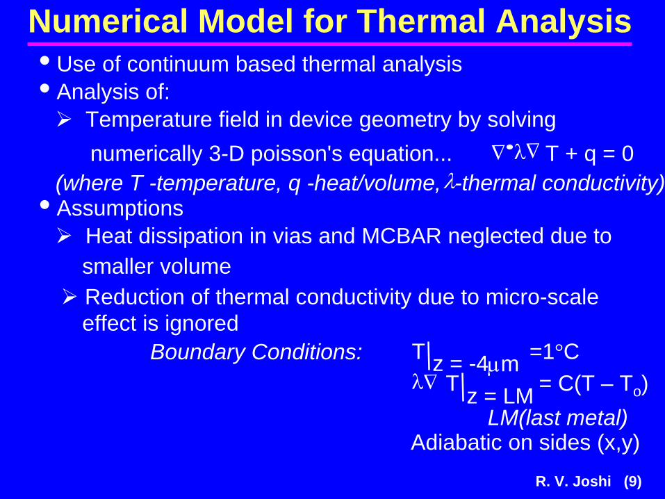
Numerical Model for Thermal Analysis• Use of continuum based thermal analysis• Analysis of:
Temperature field in device geometry by solvingnumerically 3-D poisson's equation... λ T + q = 0
(where T -temperature, q -heat/volume, λ-thermal conductivity)
Δ Δ
• AssumptionsHeat dissipation in vias and MCBAR neglected due tosmaller volumeReduction of thermal conductivity due to micro-scaleeffect is ignored
Boundary Conditions: T =1°Cλ T = C(T – To )
Δz = -4μmz = LM
LM(last metal)Adiabatic on sides (x,y)

R. V. Joshi (10)
Physical Design Used in the Thermal Model
BOXSTIBodyChannelPCMCBARCAM1V1M2V2M3V3M4V4M5
0.40.20.20.10.20.30.60.40.70.40.70.50.70.60.70.8
0.150.260.250.251.1
0.441.350.5
2.240.5
1.350.752.6
SiOSiO
SiSi
SilicideTungstenTungsten
Cu / AlC
22
u / AlCu / AlCu / AlCu / AlCu / AlCu / AlCu / AlCu / Al
1.41.412012040
170170
390 / 210390 / 210390 / 210390 / 210390 / 210390 / 210390 / 210390 / 210390 / 210
0.06**
0.0136
0.0218
0.0268
0.0444
0.0154
Layer Thickness(μm)
Width(μm)
Material ThermalConductivity
(W/m-°C)
Volumetricheating
(mW/ m )μ 3
**heat dissipation per μm of channel width.

R. V. Joshi (11)
Temperature Distribution• Four finger active• Metal interconnect (MCBAR to M5) with four fingers active.
High temperaturesare limited to body compared to interconnects
R. V. Joshi, S. Kang, C. Chuang,, SISPAD 2001, pp. 242-245.
SiO2 Dielectric (k = 1.4 W/m-K)
0
2
4
6
8
10
12
0 2 4 6 8 10Number of Active Fingers
JunctionM1
Bulk Devices
Copper Interconnect
Tem
pera
tur e
Rise
(° C)

R. V. Joshi (12)
Temperature Measurement Techniques
Use of Poly gate resistor as a sensor for temperature rise
• Device Leakage Based Temperature Measurement
R. V. Joshi (13)
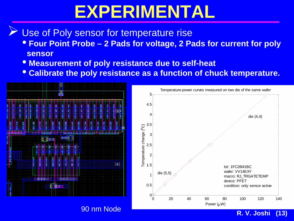
EXPERIMENTALUse of Poly sensor for temperature rise • Four Point Probe – 2 Pads for voltage, 2 Pads for current for poly sensor
• Measurement of poly resistance due to self-heat• Calibrate the poly resistance as a function of chuck temperature.
0 20 40 60 80 100 120 1400
0.5
1
1.5
2
2.5
3
3.5
4
4.5
5Temperature-power curves measured on two die of the same wafer
Power (μW)
Tem
pera
ture
cha
nge
(o C)
die (4,4)
die (5,5) lot: 1FC28I41BCwafer: VV14EXYmacro: RJ_TRGATETEMPdevice: PFETcondition: only sensor active
90 nm Node

R. V. Joshi (14)
Temperature Measurement Techniques
Use of Poly gate resistor as a sensor for temperature rise
Device Leakage Based Temperature Measurement

R. V. Joshi (15)
Leakage Based Temperature Modeling
• Leakage varies super linearly with temperature and power supply voltage– However, on chip variations of temperature and
voltage are limited– Leakage as a function of temperature and voltage
is modeled as a second order
]
1)[0,0(),(
12
21
221
VTcVbVb
TaTaITVI
ΔΔ+Δ+Δ+
Δ+Δ+=ΔΔ
Su et al.,” Full chip lekage estimation, considering power supply and temperature variation” ACM Intl. Low Power Symp. 2003, pp.210-215.
R. V. Joshi (16)
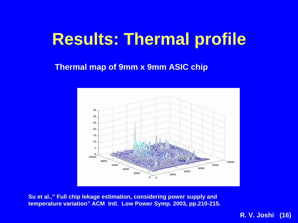
Results: Thermal profileThermal map of 9mm x 9mm ASIC chip
Su et al.,” Full chip lekage estimation, considering power supply and temperature variation” ACM Intl. Low Power Symp. 2003, pp.210-215.

R. V. Joshi (17)
3-D Modeling of Interconnects• 3-D Temperature Modeling for Interconnects:
• Development of a tool to model thermal effects
• Impact of various variables on Temperatures
Joule heating in the backend (electrical resistance increaseswith T – nonlinear).Low-k materials (Thermal conductivity scales with k).Heat flow through the interconnect (complex geometry).Use of thermal vias and design rules to minimize temperature rises (optimization).
D. Celo, et al.,” Backend implications for thermal effects in 3D integrated SOI structures,” Advanced Interconnect Conference, 2003, pp.200-206.

R. V. Joshi (18)
Modeling approaches • A number of approaches to the analysis of this heating in electrical devices have been taken including analytical and numerical models.
• The problem is quite complex with a need to solve both the device heating on the surface of the wafer and the line heating in the backend itself.
• The physics involved in solving for the conductive heat flow in a VLSI structure requires solving the following partial differential equation:
•gdev – constant, α = TCR

R. V. Joshi (19)
Atar – A thermal simulator • Our solution to this problem is a simulator that given a technology description and layout information will automatically generate a 3D model of the device, discretize the model, and solve for the temperature distribution in the device.
• Atar is thermal simulation tool that uses a technology description and layout information to automatically generate a full 3D model, complete with discretization, and then solves for the temperature distribution.
• Very flexible non-uniform, multi-model meshing allowing for meshes spanning the deep-submicron to the package.
• Produces a self-consistent solution incorporating the temperature dependance of the ohmic heating in the lines.
D. Celo, et al.,” Backend implications for thermal effects in 3D integrated SOI structures,” Advanced Interconnect Conference, 2003, pp.200-206.

R. V. Joshi (20)
3D Silicon on Insulator Technology• 3D integration scheme
• Bonding of SOI based devices directly on top of the backend of SOI devices.
• The bonding layer used in this scenario is a thin dielectric layer (0.3 mm thick).

R. V. Joshi (21)
Atar Model of 2 layer deviceSide and perspective view of Atar model with filling material
being removed
Side view perspective view

R. V. Joshi (22)
Atar Model of 4 layer device • Perspective view of four layer structure with bonding layers shown.

R. V. Joshi (23)
Results: Typical Contour Plots• Temperature contours simulated with Atar for two layer device.
Side View top Device View

R. V. Joshi (24)
Results: Joule heating in the backend • Volumetric heat dissipation in the metal were assigned varying from 0.0136 to 0.0444 mW/μm3 corresponding to M1 through to M4.
• TCR (Temp. Coeff. Of resistivity) value of Copper = 0. 43%/K
• Temperature increase due to the effect of ρ=f(T) is in the range of 6% for a structure with two stacked devices and increases for number of device
stack increases.
D. Celo, et al.,” Backend implications for thermal effects in 3D integrated SOI structures,” Advanced Interconnect Conference, 2003, pp.200-206.

R. V. Joshi (25)
Temperature as Function of the Number of Device Layers
• Plot of the nodal temperatures in the vertical z-direction from 10 μm below the silicon to the top of the backend
• Four models with 1-4 Device Layers
• Three and four level devices are becoming quite hot(unaccaptable)
•Temp drop as a function z is due to the heat spreading to ambient

R. V. Joshi (26)
The Effect of low-k Materials
• Much lower thermal conductivity then SiO2.
• Two device layer structure plotted in z-direction variety of thermal conductivities.
• Dramatic increase in temperature rise.

R. V. Joshi (27)
The Effect of low-k Materials• Much worse for one to four stacked devices
• 75K rises are occurring with a 25% reduction in the thermal conductivity of the backend material for even two layer device
• Three and four level structures above 200K rises

R. V. Joshi (28)
Removing Local Interconnect Layers • Two device layer structure
• Linear Variation as local interconnect layers removed.
• Almost 50% reduction in temperature of top device.
•Larger no. metal layer means more oxide on the active device.• Thicker oxide means increase in temperature.

R. V. Joshi (29)
Off-setting the Top Device • Two device layer structure
• Two cases 1) bottom device powered; 2) bottom device off.
• Substantial drop in temperature is obtained if the device is offset by 20 μm or more
• Cooling effect at zero offset due the local interconnect forcase 2 (lower device off).

R. V. Joshi (30)
Device Layout and Backend Structure
• The examples before were worst case simulations (stacked high powered devices)
• Possible solutions to lower these temperature rises?
• Reduce the number of local layers of interconnect from 4 to 3-1 and decrease thermal resistance to Si substrate.
• Use design rules to disallow stacking and forcing a minimumoffset between devices.
• Use of metal lines as heat spreaders and thermal vias.
D. Celo, et al.,” Backend implications for thermal effects in 3D integrated SOI structures,” Advanced Interconnect Conference, 2003, pp.200-206.

R. V. Joshi (31)
Effect of Nearby line
• Atar model built with upper layer metal line present.
• Two cases powered and un-powered bottom device.
• This line can have one of two effects on the simulation.
• Heat Spreader (line un-powered)
• Heater (line powered)
R. V. Joshi (32)
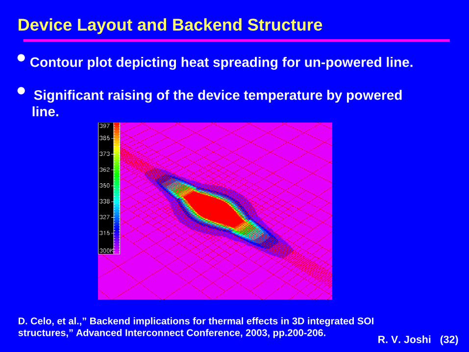
Device Layout and Backend Structure
• Contour plot depicting heat spreading for un-powered line.
• Significant raising of the device temperature by powered line.
D. Celo, et al.,” Backend implications for thermal effects in 3D integrated SOI structures,” Advanced Interconnect Conference, 2003, pp.200-206.

R. V. Joshi (33)
Device Layout and Backend Structure
• Offset of 100 μm is need to reduce the heating effect to negligible level.
• Cooling effect less significant.
R. V. Joshi (34)
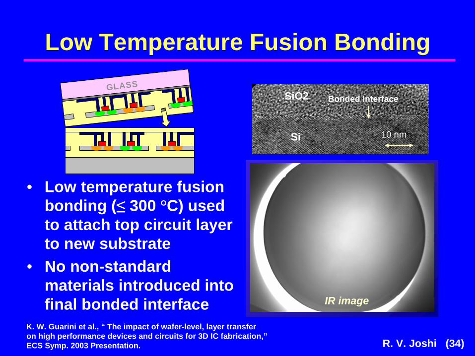
Low Temperature Fusion Bonding
• Low temperature fusion bonding (≤
300 °C) used
to attach top circuit layer to new substrate
• No non-standard materials introduced into final bonded interface
GLASS
Si
SiO2 Bonded Interface
10 nm
IR image
K. W. Guarini et al., “ The impact of wafer-level, layer transfer on high performance devices and circuits for 3D IC fabrication,”ECS Symp. 2003 Presentation.

R. V. Joshi (35)
Thermal Impact on Device/Circuit Performance• SOI BOX thickness: ~150 nm (originally) 500 nm (after transfer)• Long-channel FET and back-end characteristics undisturbed • Some degradation in short channel device behavior attributed to device
self heating
LINEAR SATURATION
K. W. Guarini et al., “ The impact of wafer-level, layer transfer on high performance devices and circuits for 3D IC fabrication,” ECS Symp. 2003 Presentation.

R. V. Joshi (36)
• SOI temperature depends strongly on BOX thickness and heater size
Input power density 0.1
mW/μm2
• Clock buffer circuit performance degrades 1.2 % per 10 oC change in SOI temperature
•Thermal Impact on Device/Circuit Performance

R. V. Joshi (37)
Analytical Die Temperature Model (1)
Analytical Die Temperature Model (1)•
••
Heat Sink
Package
Si_1Cu + ILDP1
j=1
Si_2Cu + ILD
P2j=2
Temperature Rise of the jth Active Layer in an n-layer 3-D Chip
∑ ⎥⎦⎤
⎢⎣⎡
⎟⎠⎞
⎜⎝⎛ ∑=Δ
= =
j
i
n
ik
kij A
PRT1
n = Total Number ofActive Layers
Ri = Thermal Resistance Between Adjacent Layers
Pk = Power Dissipation in the kth Layer
No Interconnect Joule Heating
( S. Im and K. Banerjee IEDM 2000)

R. V. Joshi (38)
Case Study : Wafer-Bonded Two-Layer 3-D ICsCase Study : Wafer-Bonded Two-Layer 3-D ICs
Case I
550 μm
(P. Ramm et al., 1997)
Glue Layer2 μm
Cu + ILD
Si_2 10 μm
Si_1
Cu + ILD
Wafer Bonding with Glue Layer(Usage of polymer adhesive)
Inter-WaferVia Si_2
Cu + ILD
Inter-WaferVia
Si_1
Cu + ILDAir Air 1.4 μmCu CuCu
Case II (A. Fan et al., 1999)
Metal Thermocompression Bonding
( S. Im and K. Banerjee IEDM 2000)

R. V. Joshi (39)
Case Study : Wafer-Bonded Two-Layer 3-D ICs Full Chip Simulation Case Study : Wafer-Bonded Two-Layer 3-D ICs Full Chip Simulation
0.30 0.40 0.50 0.60150
200
250
300
350
400
Tem
pera
ture
[°C
]
Power Density (3-D) [W/mm2]0.30 0.40 0.50 0.600.30 0.40 0.50 0.60
150
200
250
300
350
400
150
200
250
300
350
400
Tem
pera
ture
[°C
]
Power Density (3-D) [W/mm2]
TSi_1 (Case I & II)
Tmax (Case I) TSi_2 (Case I)Tmax (Case II) TSi_2 (Case II)
Interconnect Joule Heating Included
Each Layer Based on ITRS 100 nm node
Φ2D < Φ3D < 2 Φ2DΦ2D= 0.3 W/m2
( S. Im and K. Banerjee IEDM 2000)
•Φ3D
Heat sink- Si_1 layer only. Thus, Tmax occurs at top layer

R. V. Joshi (40)
Case Study : Wafer-Bonded Two-Layer 3-D ICs Temperature Distribution Case Study : Wafer-Bonded Two-Layer 3-D ICs Temperature Distribution
0 5 10 15 20 25 30280
300
320
340
360
380
400
420
Distance from Substrate [μm]
Tem
pera
ture
[°C
]
0 5 10 15 20 25 30280
300
320
340
360
380
400
420
Distance from Substrate [μm]
Tem
pera
ture
[°C
]
Si_2
Si_1
Case I
Case II
Case I
404 °C
317 °C
Case II
399 °C
317 °C
Φ3D ≈
2 Φ2D( S. Im and K. Banerjee IEDM 2000)

R. V. Joshi (41)
Impact of Electrothermal Coupling on 3D ICs
(K. Banerjee et al., IEDM 2003)

R. V. Joshi (42)
Summary• 3-D thermal analysis shows significant coupling between
adjacent fingers of multi-finger SOI devices. The junction
temperature rise in multi-finger devices was a factor of
three higher than single finger devices.
• Junction temperature rise in SOI due to self-heating in
high power devices like clock buffers can be 100-200C.
• Conduction from the channel can raise the M1 temperature
10°C above that of the silicon.
• Self-heating degrades the performance incrementally.

R. V. Joshi (43)
SUMMARY OF 3-D Modeling
• Simulation results clearly indicate the importance of the thermal effects in 3D integration structure.
• The inclusion of Joule heating in the backend is found to be important.
• Detailed thermal analysis needs to be performed in early design stages including choice of materials.
• Layout issues and design rules need to be analysed in the light of thermal impact.

R. V. Joshi (44)
SUMMARY OF 3D (Cu BONDED)SUMMARY OF 3D (Cu BONDED)Analytical Modeling and Full Chip Thermal Analysis of 3-D ICs
Peak Temperature Increases Linearly with Number of LayersCu-Bonded 3-D ICs Show Better Thermal Performance
Advancement in Chip Packaging / Cooling Technology and Thermal Properties of Low-k Dielectric Materials Needed for Both 2-D and 3-D ICs
( S. Im and K. Banerjee IEDM 2000)
R. V. Joshi (45)
Summary• Temperature Measurement techniques are shownto evaluate device/chip temperatures.
• 3-D Real devices using bonded Si show some signs ofSelf-heating effect (as an indirect measure of degradationin circuit/device performance).
• Electrothermal coupling is important in predicting the junction temperature.
• Further Work is essential to understand the thermaleffect at device and circuit level.

R. V. Joshi (46)
ReferencesP. Ramm et al., “ 3-D metallization for vertically integrated Circuits,” Microelectronics Eng.
37/38, 1997, pp.39-47.
R. J. Gutmann et al.,”3D Ics: A technology platform for integrated systems and opportunities for new polymeric adhesives,” Proc. IEEE Intl.of Conf. On Polymers and adhesives in microelectronics and photonics, 2001, pp.173-180.
K. W. Guarini et al.,” Electrical Integrity of state of the art 0.13 mm SOI CMOS devices and circuits transferred to 3-D integrated circuit fabrication,” IEDM Tech Digest, 2003, pp. 943- 945.
K. W. Guarini et al., “ The impact of wafer-level, layer transfer on high performance devices and circuits for 3D IC fabrication,” ECS Symp. 2003 Presentation.
D. Celo, R. V. Joshi, and T. Smy,” Backend implications for thermal effects in 3D integrated
SOI structures,” Advanced Interconnect Conference, 2003, pp.200-206.
Su, Lisa T. et. al., IEEE Transactions on Electron Devices, Vol. 41, No. 1, Jan 1994, pp. 69-75.
Workman, Glen O. et. al., IEEE Transactions on Electron Devices, Vol. 45, No. 1, Jan 1998, pp.125-133.
R. V. Joshi et al.,” 3-D thermal analysis for SOI and its impact on circuit performance,” Proc. of Int.Conf. Of Semiconductor Processes and Devices (SISPAD), 2001, pp. 242-245.
R. V. Joshi et al.,” A novel temperature measurement technique for sub-100 nm technologies,” US Patent 7176508, Feb 13, 2007.

R. V. Joshi (47)
References
K. Guarini, A. Topol, V. Chan, K. Bernstein, L. Shi, R. Joshi, W. E. Haensch, M.Ieong ,” 3D IC technology capabilities and applications,”3D Architectures for Semiconductor
Integration and Packaging Conference April 13-15, 2004.
R. Rehman and R. Reif,” Thermal analysis of 3D integrated circuits,” Proc. of International Interconnect Conf., 2001, pp. 157-159.
M. Ieong, K. Guarini, V. Chan, K. Bernstein, R. V. Joshi, J. Kedzierski, W. Haench .,” Three Dimensional CMOS Devices and Integrated Circuits,” Proc. of CICC 2003.
Su et al.,” Full chip leakage estimation, considering power supply and temperature variation” ACM Intl. Low Power Symp. 2003, pp.78-83.

R. V. Joshi (48)
Relevant Publications
S. Im and K. Banerjee, "Full chip thermal analysis of planar (2-D) and vertically integrated (3-D) high performance ICs," IEEE International Electron Devices Meeting (IEDM), pp. 727-730, 2000.K. Banerjee et al., "3-D ICs: A novel chip design for improving deep submicron interconnect performance and systems-on-chip integration," Proceedings of the IEEE, Vol. 89, pp. 602-633, 2001.K. Banerjee, S-C. Lin, A. Keshavarzi, S. Narendra and V. De, “A Self-consistent junction temperature estimation methodology for nanometer scale ICs with implications for performance and thermal management,”IEEE International Electron Devices Meeting (IEDM), pp. 887-890, 2003.