thermal conductivity and secondary porosity of single...
TRANSCRIPT

Thermal conductivity and secondary porosity of single anatase TiO2 nanowire
This article has been downloaded from IOPscience. Please scroll down to see the full text article.
2012 Nanotechnology 23 185701
(http://iopscience.iop.org/0957-4484/23/18/185701)
Download details:
IP Address: 129.186.209.173
The article was downloaded on 16/04/2012 at 14:31
Please note that terms and conditions apply.
View the table of contents for this issue, or go to the journal homepage for more
Home Search Collections Journals About Contact us My IOPscience

IOP PUBLISHING NANOTECHNOLOGY
Nanotechnology 23 (2012) 185701 (12pp) doi:10.1088/0957-4484/23/18/185701
Thermal conductivity and secondaryporosity of single anatase TiO2 nanowire
Xuhui Feng, Xiaopeng Huang and Xinwei Wang
Department of Mechanical Engineering, 2010 Black Engineering Building, Iowa State University, Ames,IA 50011, USA
E-mail: [email protected]
Received 26 December 2011, in final form 20 March 2012Published 13 April 2012Online at stacks.iop.org/Nano/23/185701
AbstractSingle anatase TiO2 nanowire is synthesized using the electrospinning technique with thesol–gel method and is suspended over a pre-processed 100 µm-wide TEM grid for furthercharacterization. The diameters of the nanowires fall in the range of 250–400 nm. Thetransient electrothermal (TET) method is adopted to acquire the voltage–time (U–t) profile ofthe Ir-coated nanowire under step Joule heating. The intrinsic thermal diffusivity of singleanatase TiO2 nanowires varies from 1.3 to 4.6× 10⁻⁶ m2 s−1, and the thermal conductivitychanges distinctly from 1.3 to 5.6 W m−1 K−1, much lower than the value of the bulkcounterpart: 8.5 W m−1 K−1. The density and thermal conductivity increase significantly withthe diameter, largely because at larger diameters less secondary porosity is left bydecomposition of organic composites and their escape from the wire during calcination. Thedensity of TiO2 nanowires is found to be much lower than that of the bulk counterpart. This issupported by the SEM image of the secondary porous surface. High secondary porosity isobserved for TiO2 nanowires, ranging from 18% to 63%. This very high secondary porosityconfirms that the decomposition of PVP content may distort the fibrous matrix and leavevacancies. In addition, the transition from amorphous to anatase phase could also create aporous state due to crystal particle aggregation.
(Some figures may appear in colour only in the online journal)
1. Introduction
Low-dimensional structures, including nanoscale films andwires/fibers/tubes, have demonstrated their intriguing nov-elties and promising applications in the electronic, optical,energy and micromechanical industries [1]. As an importantnanomaterial whose properties are significantly affectedby dimensionality [2], low-dimensional nanostructures oftitanium dioxide (TiO2) have been attracting considerableattention from both fundamental and practical perspectiveswhen the particle size, crystalline state and morphology arealtered [3, 4]. TiO2-based catalyst was first commerciallyapplied in the 1970s for air pollution control equipment [5].More intensive and in-depth applications of TiO2 materialscan also be found in photocatalytic decontamination [6],sensor materials [7, 8], dye-sensitized solar cells [9] andphotoelectrochemical cells [10]. A variety of techniques havebeen employed for synthesizing TiO2 nanostructures, such as
the sol–gel method [11–14], hydrothermal reaction [15–21],anodic oxidation [22–26], electrospinning [27–31], and manyothers [32–41]. The properties of TiO2 nanostructures varysubstantially with the synthesis method [42] and largecollections of studies and achievements have been reportedregarding their electrical and thermal properties and howthey are influenced by various TiO2 nanostructures. Bermanand Forster [43] conducted measurements on the thermalconductivity of several dielectric crystals including TiO2rutile. They concluded that limitations in the isotopic speciesof the chemical elements in the crystal caused it to behavedifferently from the Peierls predicted thermal conductivitycurve for perfect crystals. Matsuda [5] found that the thermalstability limit temperature of TiO2 is around 700–800 ◦Csince sintering is accomplished by crystalline transitionfrom anatase to rutile at about 700 ◦C. For utilizationin dye-sensitized solar cells, TiO2 nanowires were treatedwith Nb(Oet)5 solutions and it was confirmed in Beppu’s
10957-4484/12/185701+12$33.00 c© 2012 IOP Publishing Ltd Printed in the UK & the USA

Nanotechnology 23 (2012) 185701 X Feng et al
work [44] that they have high heat resistant properties anda distinct fiber shape when heated up to 450 ◦C, whichconsequently increases the electron diffusion coefficient andphotoelectrical conversion efficiency. Lambropoulos [45]measured the thermal conductivity of TiO2 thin films andthe results demonstrated that with a silicon substrate, TiO2thin film has a thermal conductivity lower than the bulkvalue by more than one order of magnitude. Wu et al[46] studied the thermal conductivity of electron-beam-(EB-) deposited and ion-plated (IP) thin films of TiO2.The properties of EB-deposited and IP processed TiO2 are0.25 and 0.45 W m−1 K−1, respectively. Lee’s work [47]indicated that for sputtered TiO2 thin films, the thermalconductivity is highly dependent on the substrate temperaturesince the substrate temperature strongly influences the grainsize and also decreases the density of atomic-scale defects.The cross-plane thermal conductivities of highly orderedamorphous and crystalline mesoporous TiO2 thin films weremeasured for porosities of 30% and 35% [58]. The thermalconductivity of crystalline sol–gel mesoporous TiO2 thin filmwas found to be about 1.06 W m−1 K−1 and a comparisonwas made to show that the connectivity and size of thecrystalline domains can provide control over the thermalconductivity in addition to the porosity. These investigationson various forms of TiO2 material lead to a conclusionthat the thermal properties of TiO2 materials are stronglyrelated to the crystalline morphology, mesoscopic structureand macroscopic form.
Although intensive attention has been devoted to studiesof TiO2 nanostructures, most work concentrates on nanofilmsand nanowire arrays, both of which contain numerousnanowires and nanofibers, and no results have been presentedconcerning the thermophysical properties of single TiO2nanowire. The way in which the polymorph structureof single TiO2 nanowire affects its thermal performanceremains uninvestigated. Additionally, as a crucial physicalproperty, the density has drawn little attention when TiO2emerges in different forms and structures. To fulfil thesepurposes, in this work single anatase TiO2 nanowire issynthesized using the electrospinning method and investigatedusing the transient electrothermal (TET) technique [48]characterization combined with a calibration procedure tounderstand the thermophysical properties and porosity inthis specific crystalline structure. In previous work [49]we employed the TET technique to investigate the thermalconductivity of thin films composed of TiO2 nanofibers andthe value was found to be much lower than that of a densestate. Modifications are made to make the TET techniqueand calibration procedure more specifically suitable for thesamples in this study and are presented in section 2. Thermalproperty analysis and discussion of the secondary porosity areincluded in section 3.
2. Experimental details
2.1. Anatase TiO2 nanowire fabrication
Because of the extremely small scale, preparation of singleTiO2 nanowires requires very delicate and complicated
processes. Figure 1 presents the whole sample preparationprocedure including the electrospinning technique setup, thecoating of iridium film over the nanowire, the focusedion beam- (FIB-) assisted platinum soldering process andthe final configuration of the testing device. In order tosynthesize parallel TiO2 nanowires for further manipulationand characterization, the electrospinning technique, as amanageable and efficient technique to synthesize fibularnanostructures, is employed in this work and the experimentalsetup is indicated in figure 1(a). 1.5 g of titaniumtetraisopropoxide (Ti(OiPr)4, from Aldrich) was mixed with3 ml of ethanol and 3 ml of acetic acid in a beaker. After10 min the mixture was moved into 7.5 ml of ethanol thatcontained 4.5 g of poly(vinyl pyrrolidone) (PVP, Aldrich, Mw1300 000), followed by magnetic stirring in a capped vial.The well-stirred solution was immediately transferred intoa syringe that was equipped with a 23-gauge stainless-steelneedle. The needle tip was connected to a 20 kV ultra-highvoltage source. A piece of transmission electron microscopy(TEM) grid with two 1.5 mm × 0.1 mm slots was pre-coatedwith gold to make only one slot nonconductively open andwas then positioned about 8–10 cm below the needle. Thetwo slots acted as symmetric collectors to create a symmetricelectrical force to collect highly oriented nanowires. With asymmetric ultra-high electric field of about 2 kV cm−1, thepolymer solution was ejected from the needle tip, stretchedinto continuous ultrathin wires and then deposited with ahighly oriented alignment [50]. The as-spun nanowires werethen placed in open air for 5 h to achieve complete hydrolysis,followed by 3 h of calcination at 500 ◦C to remove the PVPcontent. During calcination, size reduction was observed asmentioned in our previous work because of the decompositionof PVP content [49]. This process potentially causes internalstructure irregularities and defects, inducing certain impactson the material properties. After selective removal of the othernanowires with tweezers, only one nanowire was left overthe slot for later processing and characterization, as presentedby the TEM grid in figure 1(b). A slight modification fromour previous experiment is that iridium sputter coating wasapplied in this work (by a Q150T sputter coater) over theTiO2 nanowire for electrical conducting purposes, insteadof gold coating [49]. Gold film is prone to a ‘micro-island’effect, causing a rough coated film surface and probably apoor electrical contact when the sample is relatively small.Comparatively, iridium film is known to be much finer andmore uniform than gold film and it improves the coatinguniformity and conducting effect significantly. In this work,the thickness of the iridium coating was roughly 15 nmand the consequent resistance was controlled from a fewthousand ohms to tens of thousands of ohms. The physicaland mathematical interpretation of the iridium film effect willbe introduced in section 3. Because the nanowire was simplysuspended over the TEM grid slot, the contact between thenanowire and the grid surface might not be good enough toeliminate/suppress the influence of contact thermal/electricalresistance. Focused ion beam-assisted platinum soldering(Quanta 3D Dual-beam system) was used to weld both endsof the nanowire to the TEM grid surface. As seen in the right
2

Nanotechnology 23 (2012) 185701 X Feng et al
Figure 1. The complete sample preparation procedure includes the following processes. (a) An electrospinning experiment to fabricateparallel TiO2 nanowires. On the right is a magnified image of a TET grid for suspending deposited parallel samples. (b) An iridium sputtercoater for sputter coating a thin iridium film over the single TiO2 nanowire; on the right is a magnified picture of the working slot only. (c)A focused ion beam-assisted platinum soldering process to solder both ends for the purpose of better electrical and thermal conduction. Twosoldered Pt pads are shown to cover both ends of the nanowire on the slot in the right image, (d) The whole piece of TEM grid withIr-coated and Pt-soldered TiO2 nanowire is transferred onto a testing stage for further thermal characterization. On the right is an SEMimage of the fully prepared TiO2 nanowire, which is marked as sample 7 in this experiment.
image of figure 1(c), both ends of a single TiO2 nanowireare covered by deposited rectangular-shaped Pt pads. Infigure 1(d), the left image gives the overall configuration ofa testing base with the prepared TEM grid and suspendedIr-coated and Pt-soldered TiO2 nanowire. This testing base
was then moved into a vacuum chamber for further thermalcharacterization. As discussed before, due to the extremelylow pressure, convective heat transfer is minimized. Forthe radiation heat transfer, our previous work has provideddetailed analysis about its impact in the TET experiment [57].
3
Nanotechnology 23 (2012) 185701 X Feng et al
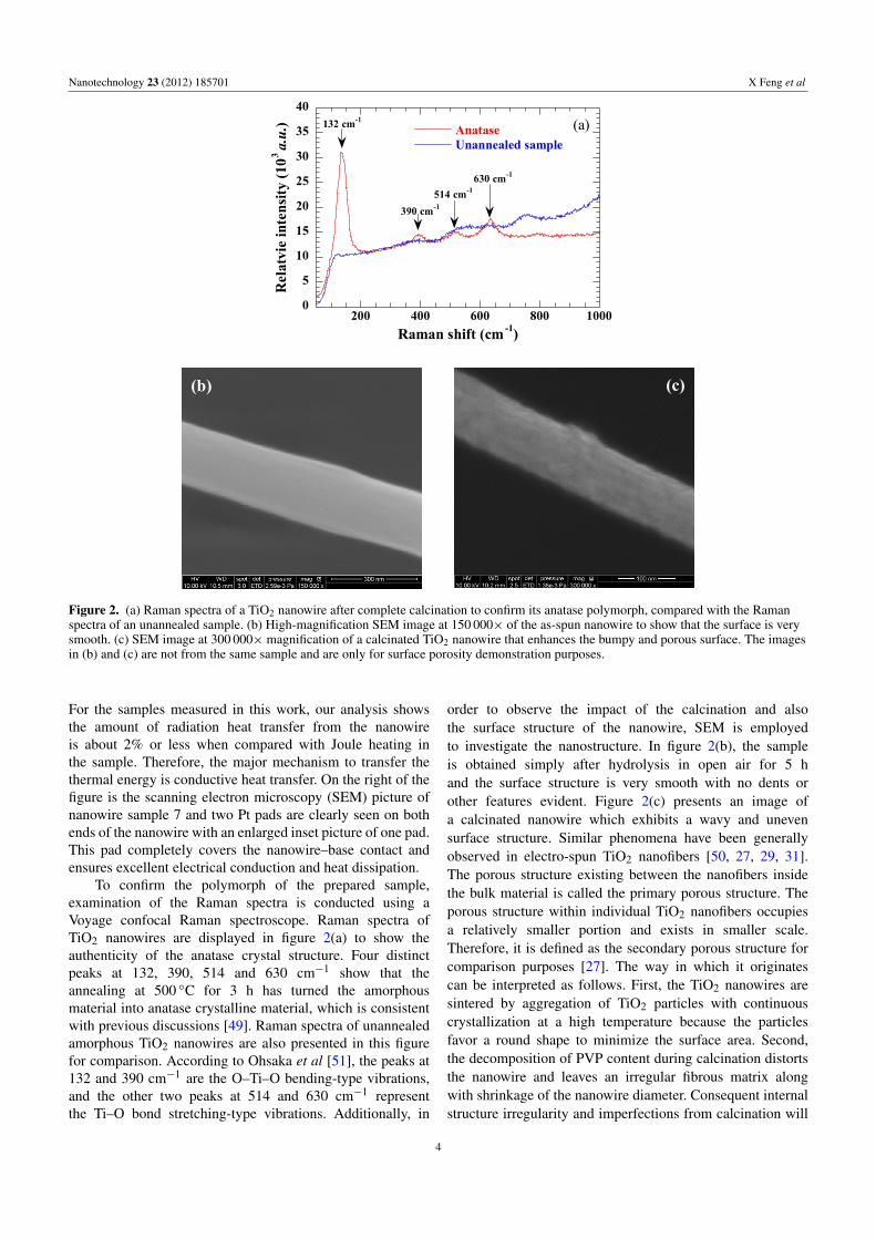
Figure 2. (a) Raman spectra of a TiO2 nanowire after complete calcination to confirm its anatase polymorph, compared with the Ramanspectra of an unannealed sample. (b) High-magnification SEM image at 150 000× of the as-spun nanowire to show that the surface is verysmooth. (c) SEM image at 300 000× magnification of a calcinated TiO2 nanowire that enhances the bumpy and porous surface. The imagesin (b) and (c) are not from the same sample and are only for surface porosity demonstration purposes.
For the samples measured in this work, our analysis showsthe amount of radiation heat transfer from the nanowireis about 2% or less when compared with Joule heating inthe sample. Therefore, the major mechanism to transfer thethermal energy is conductive heat transfer. On the right of thefigure is the scanning electron microscopy (SEM) picture ofnanowire sample 7 and two Pt pads are clearly seen on bothends of the nanowire with an enlarged inset picture of one pad.This pad completely covers the nanowire–base contact andensures excellent electrical conduction and heat dissipation.
To confirm the polymorph of the prepared sample,examination of the Raman spectra is conducted using aVoyage confocal Raman spectroscope. Raman spectra ofTiO2 nanowires are displayed in figure 2(a) to show theauthenticity of the anatase crystal structure. Four distinctpeaks at 132, 390, 514 and 630 cm−1 show that theannealing at 500 ◦C for 3 h has turned the amorphousmaterial into anatase crystalline material, which is consistentwith previous discussions [49]. Raman spectra of unannealedamorphous TiO2 nanowires are also presented in this figurefor comparison. According to Ohsaka et al [51], the peaks at132 and 390 cm−1 are the O–Ti–O bending-type vibrations,and the other two peaks at 514 and 630 cm−1 representthe Ti–O bond stretching-type vibrations. Additionally, in
order to observe the impact of the calcination and alsothe surface structure of the nanowire, SEM is employedto investigate the nanostructure. In figure 2(b), the sampleis obtained simply after hydrolysis in open air for 5 hand the surface structure is very smooth with no dents orother features evident. Figure 2(c) presents an image ofa calcinated nanowire which exhibits a wavy and unevensurface structure. Similar phenomena have been generallyobserved in electro-spun TiO2 nanofibers [50, 27, 29, 31].The porous structure existing between the nanofibers insidethe bulk material is called the primary porous structure. Theporous structure within individual TiO2 nanofibers occupiesa relatively smaller portion and exists in smaller scale.Therefore, it is defined as the secondary porous structure forcomparison purposes [27]. The way in which it originatescan be interpreted as follows. First, the TiO2 nanowires aresintered by aggregation of TiO2 particles with continuouscrystallization at a high temperature because the particlesfavor a round shape to minimize the surface area. Second,the decomposition of PVP content during calcination distortsthe nanowire and leaves an irregular fibrous matrix alongwith shrinkage of the nanowire diameter. Consequent internalstructure irregularity and imperfections from calcination will
4
Nanotechnology 23 (2012) 185701 X Feng et al
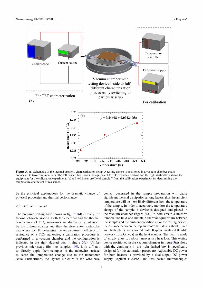
Figure 3. (a) Schematic of the thermal property characterization setup. A testing device is positioned in a vacuum chamber that isconnected to two equipment sets. The left dashed box shows the equipment for TET characterization and the right dashed box shows theequipment for the calibration experiment. (b) A fitted linear profile of sample 7 from the calibration experiment for determining thetemperature coefficient of resistance.
be the principal explanations for the dramatic change ofphysical properties and thermal performance.
2.2. TET measurement
The prepared testing base shown in figure 1(d) is ready forthermal characterization. Both the electrical and the thermalconductance of TiO2 nanowires are dramatically enhancedby the iridium coating and they therefore show metal-likecharacteristics. To determine the temperature coefficient ofresistance of a TiO2 nanowire, a calibration procedure isperformed in a vacuum chamber and the configuration isindicated in the right dashed box in figure 3(a). Unlikeprevious microscale film-like samples [49], it is difficultto directly apply thermocouples to the nanowire surfaceto sense the temperature change due to the nanometerscale. Furthermore, the layered structure at the wire–base
contact generated in the sample preparation will causesignificant thermal dissipation among layers, thus the ambienttemperature will be most likely different from the temperatureof the sample. In order to accurately monitor the temperaturechange of the sample, a device is designed and placed inthe vacuum chamber (figure 3(a)) to both create a uniformtemperature field and maintain thermal equilibrium betweenthe sample and the ambient conditions. For the testing device,the distance between the top and bottom plates is about 1 inchand both plates are covered with Kapton insulated flexibleheaters (from Omega) as the heat sources. The wall is madeof acrylic glass to reduce unnecessary heat loss. This testingdevice positioned in the vacuum chamber in figure 3(a) alongwith the equipment in the right dashed box is specificallydesigned for the calibration procedure. Adjustable DC powerfor both heaters is provided by a dual-output DC powersupply (Agilent E3649A) and two pasted thermocouples
5

Nanotechnology 23 (2012) 185701 X Feng et al
are connected to a programmable temperature controller(Stanford Research Systems) to monitor the temperaturethrough the whole calibration process. The calibration processis performed when the temperature descends from about50 ◦C to room temperature. During the cooling process,limited power is provided from the power supply to ensurethat the whole process is slow and moderate so that theassumption of quasi-equilibrium is appropriate to describethis calibration procedure. Taking sample 7 for instance, itstypical calibration curve is shown in figure 3(b), in whichthe resistance reduces from about 12 440 to 12 250 � whilethe temperature decreases from 321 to 307 K. Linear fittingis established based on the recorded data and the deviationfrom standard metal-like resistance–temperature properties isprobably attributed to the structure of the Ir on the nanowiresurface. The fitted temperature coefficient of resistance forsample 7 is about 12.4� K−1 and it is adopted to evaluate thetemperature change during the transient heating process. Thistemperature change could eventually be applied to calculatethe effective thermal conductivity of the nanowire. To measurethe thermal diffusivity, TET characterization is also performedwhen the testing base is placed in the same device whilethe measurement is switched to another setup shown in theleft box in figure 3(a). A current source (Keithley 6221)is connected to the testing base to supply a step currentand an oscilloscope (Tektronix TDS 7054 digital phosphoroscilloscope) is employed to monitor and record the inducedreal-time voltage–time (U–t) profiles. The current should becontrolled to provide a response that is strong enough to becaptured and analyzed but also to keep the sample structureintact. Meanwhile, the frequency must also be appropriate tohave a useful profile that contains both rising state and steadystate.
3. Results and discussion
3.1. Physical model of the TET technique
The effectiveness of the TET technique for measuring thethermal properties of conductive, semi-conductive and evennonconductive materials has been introduced in previouswork [48, 49]. With an appropriately coated conductive layer,semi-conductive and nonconductive wires exhibit distinctelectrical conductive properties and provide signals strongenough for detection. A schematic of the TET experimentalsetup is shown in the left dashed box in figure 3(a). Thesample is housed in a vacuum chamber whose pressure isbelow 10−3 Torr to suppress heat convection to a negligiblelevel. Meanwhile, the heat transfer by radiation is alsonegligible from previous discussion [57]. The physical modelof the TET technique is developed based on one-dimensionalheat conduction theory [49]. The electric heating q0 isassumed constant and both ends of the sample are consideredto have constant temperature since the aluminum stage islarge enough to dissipate the heat compared with the size ofthe sample. When the convection effect is negligible under1 mTorr, the governing equation is expressed as
∂(ρcpT)
∂t= k
∂2T
∂x2 + q0, (1)
where ρ, cp and k are the density, specific heat andthermal conductivity of the sample, respectively. The detailedprocedure to solve this governing equation is given in Guo’swork [48]. Only the expression of the temperature distributionis presented here for further analysis purposes,
T(t) =1L
∫ L
x=0T(x, t) dx = T0 +
8q0L2
kπ4
×
∞∑m=1
1− exp[−(2m− 1)2π2αt/L2]
(2m− 1)4. (2)
When the temperature distribution along the sample reachesthe steady state, the average temperature of the wire becomesT0 + q0L2/(12k). q0 is the electrical heating power per unitvolume and can be expressed as q0 = Q/(LA) = I2R/(LA),while Q is the electrical heating power and A and L are thecross-sectional area and length of the sample, respectively.With the calibration result for the temperature coefficientof resistance η and the resistance change 1R during theheating process, the temperature change 1T = Tsteady − T0 iscalculated and then the thermal conductivity is obtained as k =QL/(12A1T). Meanwhile, the dimensionless temperatureincrease is written as
T∗ =96
π4
∞∑m=1
1− exp[−(2m− 1)2π2αt/L2]
(2m− 1)4. (3)
The voltage evolution (Usample) recorded by the oscilloscopeis directly related to the average temperature change of thesample as
Usample = IR0 + Iη8q0L2
kπ4
×
∞∑m=1
1− exp[−(2m− 1)2π2αt/L2]
(2m− 1)4, (4)
where Usample is the voltage over the sample recorded bythe oscilloscope, I is the constant current fed through thesample and R0 is the resistance of the sample withoutheating. It is important to observe that the measuredvoltage change (equation (4)) and the normalized temperaturechange (equation (3)) share an identical term, in whichthe thermal diffusivity is contained. In our work, first weobtain the normalized temperature rise based on the measuredU–t profile. Then theoretical prediction is conductedusing equation (3) based on a guessed thermal diffusivity andis compared with the experimental result. The value of thermaldiffusivity giving the best fit (least squares method) of theexperimental result is taken as the thermal diffusivity of thesample. In this work, the TET characterization is conductedat two or three different current levels for each sample toreduce possible noise and uncertainty from the equipment andenvironment.
3.2. Data processing in TET measurement
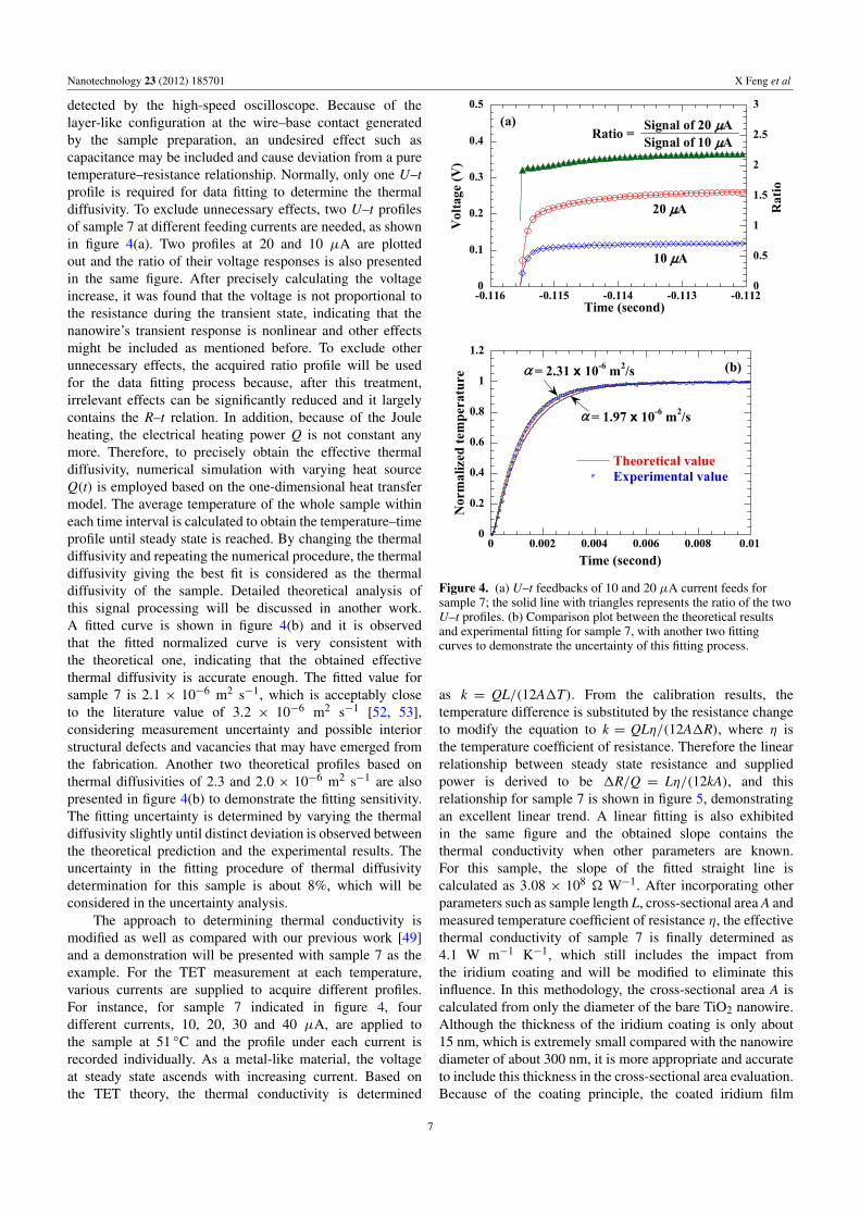
As seen in figure 4, when a step DC current providedby the current source is fed through the nanowire, aquick response of voltage evolution of the nanowire is
6
Nanotechnology 23 (2012) 185701 X Feng et al
detected by the high-speed oscilloscope. Because of thelayer-like configuration at the wire–base contact generatedby the sample preparation, an undesired effect such ascapacitance may be included and cause deviation from a puretemperature–resistance relationship. Normally, only one U–tprofile is required for data fitting to determine the thermaldiffusivity. To exclude unnecessary effects, two U–t profilesof sample 7 at different feeding currents are needed, as shownin figure 4(a). Two profiles at 20 and 10 µA are plottedout and the ratio of their voltage responses is also presentedin the same figure. After precisely calculating the voltageincrease, it was found that the voltage is not proportional tothe resistance during the transient state, indicating that thenanowire’s transient response is nonlinear and other effectsmight be included as mentioned before. To exclude otherunnecessary effects, the acquired ratio profile will be usedfor the data fitting process because, after this treatment,irrelevant effects can be significantly reduced and it largelycontains the R–t relation. In addition, because of the Jouleheating, the electrical heating power Q is not constant anymore. Therefore, to precisely obtain the effective thermaldiffusivity, numerical simulation with varying heat sourceQ(t) is employed based on the one-dimensional heat transfermodel. The average temperature of the whole sample withineach time interval is calculated to obtain the temperature–timeprofile until steady state is reached. By changing the thermaldiffusivity and repeating the numerical procedure, the thermaldiffusivity giving the best fit is considered as the thermaldiffusivity of the sample. Detailed theoretical analysis ofthis signal processing will be discussed in another work.A fitted curve is shown in figure 4(b) and it is observedthat the fitted normalized curve is very consistent withthe theoretical one, indicating that the obtained effectivethermal diffusivity is accurate enough. The fitted value forsample 7 is 2.1 × 10⁻⁶ m2 s−1, which is acceptably closeto the literature value of 3.2 × 10⁻⁶ m2 s−1 [52, 53],considering measurement uncertainty and possible interiorstructural defects and vacancies that may have emerged fromthe fabrication. Another two theoretical profiles based onthermal diffusivities of 2.3 and 2.0 × 10⁻⁶ m2 s−1 are alsopresented in figure 4(b) to demonstrate the fitting sensitivity.The fitting uncertainty is determined by varying the thermaldiffusivity slightly until distinct deviation is observed betweenthe theoretical prediction and the experimental results. Theuncertainty in the fitting procedure of thermal diffusivitydetermination for this sample is about 8%, which will beconsidered in the uncertainty analysis.
The approach to determining thermal conductivity ismodified as well as compared with our previous work [49]and a demonstration will be presented with sample 7 as theexample. For the TET measurement at each temperature,various currents are supplied to acquire different profiles.For instance, for sample 7 indicated in figure 4, fourdifferent currents, 10, 20, 30 and 40 µA, are applied tothe sample at 51 ◦C and the profile under each current isrecorded individually. As a metal-like material, the voltageat steady state ascends with increasing current. Based onthe TET theory, the thermal conductivity is determined
Figure 4. (a) U–t feedbacks of 10 and 20 µA current feeds forsample 7; the solid line with triangles represents the ratio of the twoU–t profiles. (b) Comparison plot between the theoretical resultsand experimental fitting for sample 7, with another two fittingcurves to demonstrate the uncertainty of this fitting process.
as k = QL/(12A1T). From the calibration results, thetemperature difference is substituted by the resistance changeto modify the equation to k = QLη/(12A1R), where η isthe temperature coefficient of resistance. Therefore the linearrelationship between steady state resistance and suppliedpower is derived to be 1R/Q = Lη/(12kA), and thisrelationship for sample 7 is shown in figure 5, demonstratingan excellent linear trend. A linear fitting is also exhibitedin the same figure and the obtained slope contains thethermal conductivity when other parameters are known.For this sample, the slope of the fitted straight line iscalculated as 3.08 × 10⁸ � W−1. After incorporating otherparameters such as sample length L, cross-sectional area A andmeasured temperature coefficient of resistance η, the effectivethermal conductivity of sample 7 is finally determined as4.1 W m−1 K−1, which still includes the impact fromthe iridium coating and will be modified to eliminate thisinfluence. In this methodology, the cross-sectional area A iscalculated from only the diameter of the bare TiO2 nanowire.Although the thickness of the iridium coating is only about15 nm, which is extremely small compared with the nanowirediameter of about 300 nm, it is more appropriate and accurateto include this thickness in the cross-sectional area evaluation.Because of the coating principle, the coated iridium film
7
Nanotechnology 23 (2012) 185701 X Feng et al
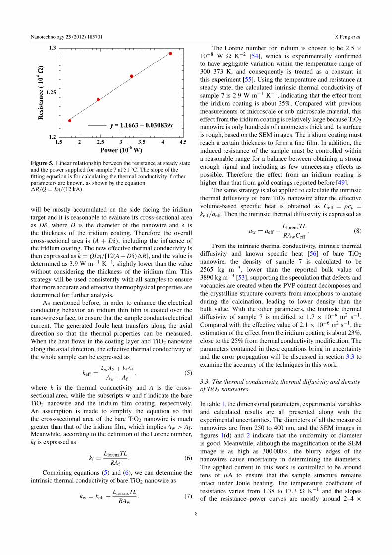
Figure 5. Linear relationship between the resistance at steady stateand the power supplied for sample 7 at 51 ◦C. The slope of thefitting equation is for calculating the thermal conductivity if otherparameters are known, as shown by the equation1R/Q = Lη/(12 kA).
will be mostly accumulated on the side facing the iridiumtarget and it is reasonable to evaluate its cross-sectional areaas Dδ, where D is the diameter of the nanowire and δ isthe thickness of the iridium coating. Therefore the overallcross-sectional area is (A + Dδ), including the influence ofthe iridium coating. The new effective thermal conductivity isthen expressed as k = QLη/[12(A+Dδ)1R], and the value isdetermined as 3.9 W m−1 K−1, slightly lower than the valuewithout considering the thickness of the iridium film. Thisstrategy will be used consistently with all samples to ensurethat more accurate and effective thermophysical properties aredetermined for further analysis.
As mentioned before, in order to enhance the electricalconducting behavior an iridium thin film is coated over thenanowire surface, to ensure that the sample conducts electricalcurrent. The generated Joule heat transfers along the axialdirection so that the thermal properties can be measured.When the heat flows in the coating layer and TiO2 nanowirealong the axial direction, the effective thermal conductivity ofthe whole sample can be expressed as
keff =kwA2 + kfAf
Aw + Af, (5)
where k is the thermal conductivity and A is the cross-sectional area, while the subscripts w and f indicate the bareTiO2 nanowire and the iridium film coating, respectively.An assumption is made to simplify the equation so thatthe cross-sectional area of the bare TiO2 nanowire is muchgreater than that of the iridium film, which implies Aw > Af.Meanwhile, according to the definition of the Lorenz number,kf is expressed as
kf =LlorenzTL
RAf. (6)
Combining equations (5) and (6), we can determine theintrinsic thermal conductivity of bare TiO2 nanowire as
kw = keff −LlorenzTL
RAw. (7)
The Lorenz number for iridium is chosen to be 2.5 ×10⁻⁸ W � K−2 [54], which is experimentally confirmedto have negligible variation within the temperature range of300–373 K, and consequently is treated as a constant inthis experiment [55]. Using the temperature and resistance atsteady state, the calculated intrinsic thermal conductivity ofsample 7 is 2.9 W m−1 K−1, indicating that the effect fromthe iridium coating is about 25%. Compared with previousmeasurements of microscale or sub-microscale material, thiseffect from the iridium coating is relatively large because TiO2nanowire is only hundreds of nanometers thick and its surfaceis rough, based on the SEM images. The iridium coating mustreach a certain thickness to form a fine film. In addition, theinduced resistance of the sample must be controlled withina reasonable range for a balance between obtaining a strongenough signal and including as few unnecessary effects aspossible. Therefore the effect from an iridium coating ishigher than that from gold coatings reported before [49].
The same strategy is also applied to calculate the intrinsicthermal diffusivity of bare TiO2 nanowire after the effectivevolume-based specific heat is obtained as Ceff = ρcp =
keff/aeff. Then the intrinsic thermal diffusivity is expressed as
aw = aeff −LlorenzTL
RAwCeff. (8)
From the intrinsic thermal conductivity, intrinsic thermaldiffusivity and known specific heat [56] of bare TiO2nanowire, the density of sample 7 is calculated to be2565 kg m−3, lower than the reported bulk value of3890 kg m−3 [53], supporting the speculation that defects andvacancies are created when the PVP content decomposes andthe crystalline structure converts from amorphous to anataseduring the calcination, leading to lower density than thebulk value. With the other parameters, the intrinsic thermaldiffusivity of sample 7 is modified to 1.7 × 10⁻⁶ m2 s−1.Compared with the effective value of 2.1× 10⁻⁶ m2 s−1, theestimation of the effect from the iridium coating is about 23%,close to the 25% from thermal conductivity modification. Theparameters contained in these equations bring in uncertaintyand the error propagation will be discussed in section 3.3 toexamine the accuracy of the techniques in this work.
3.3. The thermal conductivity, thermal diffusivity and densityof TiO2 nanowires
In table 1, the dimensional parameters, experimental variablesand calculated results are all presented along with theexperimental uncertainties. The diameters of all the measurednanowires are from 250 to 400 nm, and the SEM images infigures 1(d) and 2 indicate that the uniformity of diameteris good. Meanwhile, although the magnification of the SEMimage is as high as 300 000×, the blurry edges of thenanowires cause uncertainty in determining the diameters.The applied current in this work is controlled to be aroundtens of µA to ensure that the sample structure remainsintact under Joule heating. The temperature coefficient ofresistance varies from 1.38 to 17.3 � K−1 and the slopesof the resistance–power curves are mostly around 2–4 ×
8

Nanotechnology 23 (2012) 185701 X Feng et al
Table 1. Experimental data and calculated results for all samples.
No.Length(mm)
Diameter(nm)
DC current(µA)
1R/1T(� K−1)
1R/1Q(×108 �W−1)
Density(kg m−3)
Thermaldiffusivity(×10−6 m2 s−1)
Thermalconductivity(W m−1 K−1)
Porosity(%)
1 0.13 250± 13 18.0 5.30 2.83 1430± 180 1.3± 0.2 1.3± 0.2 632 0.11 370± 19 26.0 8.30 2.11 1620± 200 1.9± 0.2 2.1± 0.4 583 0.11 295± 15 20.0 10.6 2.03 1960± 240 4.2± 0.5 5.6± 0.9 504 0.11 383± 19 30.0 2.05 0.239 1550± 190 4.6± 0.5 4.9± 0.8 605 0.11 320± 16 16.0 13.1 4.48 2190± 270 1.5± 0.2 2.3± 0.4 446 0.11 340± 17 14.0 17.3 4.21 2300± 280 2.1± 0.2 3.4± 0.6 417 0.11 342± 17 18.0 12.4 3.08 2570± 310 1.7± 0.2 2.9± 0.5 348 0.11 360± 18 35.0 1.38 0.212 3180± 390 1.5± 0.2 3.2± 0.5 18
108 � W−1 except for two samples. The thermal propertiesand densities in this table are intrinsic values excluding theimpact from the iridium coating and are lower than theliterature values of anatase TiO2 crystal [52, 53]. As seen inthe SEM image in figure 2 and also in other publications [27,29, 31], the wavy and uneven surface structure to some extentdemonstrates that the fabricated TiO2 nanowire featuresrelatively irregular and secondary porous features comparedwith bulk material. These irregularities and vacancies aremostly generated from the removal of PVP content duringwhich the degradation may distort the fibrous matrix andalso from the aggregation of TiO2 particles in the crystallinestructure transition procedure. Using the densities, estimatesof the porosities of the nanowires are also concluded tobe from about 18% to 63%, indicating that the calcinationnot only leaves structural distortions but also remarkablevacancies, which are possibly controllable if the experimentalparameters are carefully selected [27].
The trends on how the thermal properties vary withdensity are presented in figure 6. When the density increasesfrom 1434 to 3183 kg m−3, the thermal conductivity shows adistinct increasing trend. Except for two obviously abnormalpoints that are higher than 4 W m−1 K−1, the other datapoints display thermal conductivity increases with increasingdensity and these thermal conductivity values are lowerthan the literature value of 8.5 W m−1 K−1 for the bulkmaterial [52]. As discussed before, the possible reason forthis difference is because the interior structure distortions andvacancies from calcination induce phonon-impurity/defectscattering during their transport and, thus, lower the thermalconductivity. Additionally, the intrinsic thermal conductivitiesof single TiO2 nanowires have been estimated qualitativelyin our work before [49] and the results were in the range of5–12 W m−1 K−1, which are slightly greater than the valuesin this work but still consistent considering the simplificationsmade in that model and also the existence of secondaryporous structures. The thermal diffusivity exhibits a flat trendagainst density. Within the range where the density increases,the thermal diffusivity changes from 1.3 × 10⁻⁶ to 2.1 ×10⁻⁶ m2 s−1, which is only about a 40% fluctuation andis much smaller than the thermal conductivity change. Twoexceptional points are still plotted and their irregular valuesmight be induced by strong measurement perturbation. Withhigher density, although the ability of the nanowire to conductheat is improved, the more condensed structure also reinforces
Figure 6. The thermal conductivities and thermal diffusivities ofsingle TiO2 nanowires versus density for all the samples listed intable 1. The curves are to guide the eyes to follow the data trend,with an error bar marked on each data point.
its capability to store heat. The comprehensive outcome isthat no significant visible tendency is observed with thermaldiffusivity, because the enhancements of both the capability tostore heat and the ability to conduct heat are comparable.
The diameter of a nanowire (a very typical characteristicsize) is another perspective from which to understand thethermal properties of small scale materials. In figure 7 adistinct trend is observed between density and diameter.When the diameter increases from 250 to 380 nm,the density also demonstrates a consistently ascendingprofile from 1434 to 3183 kg m−3, except for afew discrepancies. These discrepancies may come fromunexpected conditional perturbation during the experimentand dimension measurement uncertainties. This visible trendis largely caused by the crystal structure transition to alarge cluster during calcination. Larger diameters featuremore aggregated anatase crystal clusters and consequentlygive lower portions of vacancies. Accordingly the densitiesshow larger values. For the thermal transport properties, thevariation in the range of diameters is not large enough toimpose substantial impact on the thermal diffusivity when thediameter changes from 250 to 380 nm, while it is evident
9

Nanotechnology 23 (2012) 185701 X Feng et al
that this tendency is observed for the thermal conductivity.For the thermal diffusivity, when the diameter increases,only a variation of around 1–2 × 10⁻⁶ m2 s−1 is observedand it is roughly a flat trend. However, as an intrinsicproperty that does receive significant influence from thecrystal structure and imperfections, the thermal conductivitypresents stronger responses to diameter variations. As seen infigure 7, when the diameter increases from 250 to 370 nm,the thermal conductivity strongly increases from 1.3 to4.9 W m−1 K−1. This profile is still accompanied by strongfluctuations. The main explanation for the increasing trendis that a larger diameter is roughly connected to a lowerporosity, and therefore fewer vacancies or holes exist asan impediment to phonon transfer. Another possible reasonis that large nanowire diameters decrease the probabilityof phonon–surface scattering and consequently give higherthermal conductivities. Predictions can be made that if thediameter increases by more than one order of magnitude,the thermal conductivity would be affected much moresignificantly. As discussed before, because of the extremelysmall scale, dimensional measurements and experimentalconditions can both influence the experimental uncertaintyand they are the main reasons why certain anomalouspoints stand out. First, when measuring the diameter, themagnification of the SEM image was increased to 300 000×.Under this huge magnification, the edge of the nanowire wasnot sharp enough for precise measurement and the blurrycharacter causes reading errors to a certain degree. Second,although the samples were fabricated and processed in thesame way, the degree of environmental perturbation variesfrom sample to sample. After obtaining valid data for analysis,a few points appear with irregular values compared withthe majority. These points are not considered wrong butless accurate because they may have received a relativelystronger impact from experimental pertubations. They arestill plotted out for analysis purposes. Additionally, no matterhow accurate the data are, uncertainties are inevitable in themeasurements and calculations.
3.4. Uncertainty analysis
The thermal diffusivity is obtained by fitting different valuesuntil the profile with the smallest fitting error is acquired.During the fitting procedure, it is reasonable to acquire thefitting uncertainty by changing the values to observe howstrong the deviation is from the experimental profile. Whenthe value is varied over±8%, the corresponding profiles showstrong deviation from the experimental curve and thereforethe uncertainty from the data fitting is 8%, as displayedin figure 4(b). With the high-magnification SEM image,the length measurement uncertainty is as small as 1% andtherefore the L2 term brings in about a 2% uncertainty. Thusthe total uncertainty for the thermal diffusivity is about 8.3%.
Calculation of the thermal conductivity is more compli-cated as stated in previous discussion. The uncertainty of theresistance is estimated to be 5%. Therefore, the uncertainty ofthe temperature coefficient of the resistance is about 5.1%,mostly from the resistance. The uncertainty of the power
Figure 7. The thermal conductivity, thermal diffusivity and densityversus the diameter for all measured TiO2 nanowires, with lines toguide the eyes to the data trend. An error bar is shown for each datapoint.
is around 1%. The measurement of the diameter is basedon a high-magnification image and is found to have a 5%uncertainty because of the difficulty of adjusting the focus.Consequently, the total uncertainty for the effective thermalconductivity is about 9%. The uncertainty of the effectivevolume-based specific heat is also calculated to be 12.24%based on the discussion above.
The overall uncertainty of the intrinsic thermal diffusivityis 11.7%. Following the same method, the uncertaintyof the intrinsic thermal conductivity is calculated to be16.5%. From the uncertainty analysis, it is conclusivethat the uncertainties of major parameters and results inthis experiment are controlled within acceptable ranges,considering the differences among samples and varyingexperimental conditions. The uncertainties are listed intable 1, as supplements to the measurement values, along witherror bars marked in the figures for each discrete data point.
4. Conclusion
In this paper, single TiO2 nanowires, which are consideredto be the intrinsic units composing TiO2 nanofilm andnanowire arrays, were exclusively studied. Highly orientedTiO2 nanowires were first fabricated using the electrospinningtechnique and collected on a pre-processed TEM grid. Afterhydrolysis and calcination, only one TiO2 nanowire waschosen for thermal characterization. Raman spectra confirmedthe anatase polymorph of the single TiO2 nanowire. Incalcination, both decomposition of the PVP content and thetransition of the TiO2 crystalline structure occurred. These
10

Nanotechnology 23 (2012) 185701 X Feng et al
processes strongly distorted the fibrous structure and inducedobvious aggregation of the TiO2 particles, consequentlyresulting in a secondary porous structure. The porosity wasfurther evaluated by the results from thermal characterization.Via TET characterization, the obtained thermal conductivityvaried from 1.3 to 5.6 W m−1 K−1 while the density changedfrom 1430 to 3180 kg m−3, significantly lower than the bulkvalue because the structural distortions and imperfectionsstrongly hampered the phonon transport. With increasingdensity, the thermal conductivity presented an increasingtendency while the thermal diffusivity simply scattered arounda certain value, showing a flat trend. For all the samples in thiswork, the high porosity varied from 18% to 63%, showingthat the crystal structure contained substantial vacancies andspacing. The diameter of the nanowire was also investigatedto understand its relationship with the thermal properties. Therange of the diameter was from 250 to 380 nm. Within thissmall variation, the thermal conductivity showed a distincttrend with a certain fluctuation. The density changed morestrongly with the diameter, indicating that when the diametervaries, the levels of vacancies and irregularity may be affectedsignificantly.
Acknowledgments
Support of this work from the National Science Foundation(CBET-0931290) is gratefully acknowledged. The helpfrom Professor Younan Xia and his student YunqianDai with nanowire fabrication is sincerely acknowledged.We appreciate the great help from Elizabeth Welch andNathan Van Velson in proofreading the manuscript.
References
[1] Xia Y N, Yang P D, Sun Y G, Wu Y Y, Mayers B, Gates B,Yin Y D, Kim F and Yan Y Q 2003 One-dimensionalnanostructures: synthesis, characterization, and applicationsAdv. Mater. 15 353–89
[2] Hu J T, Odom T W and Lieber C M 1999 Chemistry andphysics in one dimension: synthesis and properties ofnanowires and nanotubes Acc. Chem. Res. 32 435–45
[3] Melendres C A, Narayanasamy A, Maroni V A andSiegel R W 1989 Raman-spectroscopy of nanophase TiO2J. Mater. Res. 4 1246–50
[4] Terwilliger C D and Chiang Y M 1993 Excess thermodynamicproperties of nanophase titanium-dioxide prepared bychemical and physical methods Mater. Res. S C 286 15–20
[5] Matsuda S 1983 Titanium-oxide based catalysts—a reviewAppl. Catal. 8 149–65
[6] Dagan G and Tomkiewicz M 1993 TiO2 aerogels forphotocatalytic decontamination of aquatic environmentsJ. Phys. Chem. 97 12651–5
[7] Azad A M, Akbar S A, Younkman L B and Alim M A 1994High-temperature immittance response in anatase-basedsensor materials J. Am. Ceram. Soc. 77 3145–52
[8] Azad A M, Younkman L B, Akbar S A and Alim M A 1994Characterization of TiO2-based sensor materials usingimmittance spectroscopy J. Am. Ceram. Soc. 77 481–6
[9] Bach U, Lupo D, Comte P, Moser J E, Weissortel F, Salbeck J,Spreitzer H and Gratzel M 1998 Solid-state dye-sensitizedmesoporous TiO2 solar cells with high photon-to-electronconversion efficiencies Nature 395 583–5
[10] Gratzel M 2001 Photoelectrochemical cells Nature414 338–44
[11] Lei Y, Zhang L D, Meng G W, Li G H, Zhang X Y,Liang C H, Chen W and Wang S X 2001 Preparation andphotoluminescence of highly ordered TiO2 nanowire arraysAppl. Phys. Lett. 78 1125–7
[12] Lin Y, Wu G S, Yuan X Y, Xie T and Zhang L D 2003Fabrication and optical properties of TiO2 nanowire arraysmade by sol–gel electrophoresis deposition into anodicalumina membranes J. Phys.: Condens. Matter 15 2917–22
[13] Miao L, Tanemura S, Toh S, Kaneko K and Tanemura M 2004Heating-sol–gel template process for the growth of TiO2nanorods with rutile and anatase structure Appl. Surf. Sci.238 175–9
[14] Miao L, Tanemura S, Toh S, Kaneko K and Tanemura M 2004Fabrication, characterization and raman study of anataseTiO2 nanorods by a heating-sol–gel template processJ. Cryst. Growth 264 246–52
[15] Yuan Z Y and Su B L 2004 Titanium oxide nanotubes,nanofibers and nanowires Colloid Surf. A 241 173–83
[16] Francioso L and Siciliano P 2006 Top-down contactlithography fabrication of a TiO2 nanowire array over aSiO2 mesa Nanotechnology 17 3761–7
[17] Kolen’ko Y V, Kovnir K A, Gavrilov A I, Garshev A V,Frantti J, Lebedev O I, Churagulov B R,Van Tendeloo G and Yoshimura M 2006 Hydrothermalsynthesis and characterization of nanorods of varioustitanates and titanium dioxide J. Phys. Chem. B 110 4030–8
[18] Zhang X W, Pan J H, Du A J, Fu W J, Sun D D andLeckie J O 2009 Combination of one-dimensional TiO2nanowire photocatalytic oxidation with microfiltration forwater treatment Water Res. 43 1179–86
[19] Ge Z X, Wei A X, Liu J, Zhao W and Liu C B 2010 Synthesisand photovoltaic devices performance of single crystallineTiO2 nanowire bundle arrays J. Inorg. Mater. 25 1105–9
[20] Liao J Y, Lei B X, Wang Y F, Liu J M, Su C Y andKuang D B 2011 Hydrothermal fabrication ofquasi-one-dimensional single-crystalline anatase TiO2nanostructures on FTO glass and their applications indye-sensitized solar cells Chem.—Eur. J. 17 1352–7
[21] Xu Y, Gu H S, Xia H T and Hu M Z 2011 TiO2 nanowiredye-sensitized solar cells fabricated by hydrothermalmethod 3rd Int. Photonics and Optoelectronics Mtg (Poem2010) vol 276 p 012196
[22] Lei Y, Zhang L D and Fan J C 2001 Fabrication,characterization and raman study of TiO2 nanowire arraysprepared by anodic oxidative hydrolysis of TiCl3 Chem.Phys. Lett. 338 231–6
[23] Zhang X Y, Yao B D, Zhao L X, Liang C H, Zhang L D andMao Y Q 2001 Electrochemical fabrication ofsingle-crystalline anatase TiO2 nanowire arraysJ. Electrochem. Soc. 148 G398–400
[24] Jiao Z, Wu M H, Shi L Y, Li Z and Wang Y L 2004Preparation of TiO2 nanowire by atomic force microscopyelectrochemical anode oxidation Chin. J. Inorg. Chem.20 1325–8
[25] Liu S Q and Huang K L 2005 Straightforward fabrication ofhighly ordered TiO2 nanowire arrays in AAM on aluminumsubstrate Sol. Energy Mater. Sol. Cells 85 125–31
[26] Cai F G, Yang F, Zhao Y and Cheng C H 2011 Preparation ofTiO2 nanotube and nanotube/nanowire composite arrays bytemperature control Chin. J. Inorg. Chem. 27 504–8
[27] Li D and Xia Y N 2003 Fabrication of titania nanofibers byelectrospinning Nano Lett. 3 555–60
[28] Subbiah T, Bhat G S, Tock R W, Pararneswaran S andRamkumar S S 2005 Electrospinning of nanofibers J. Appl.Polym. Sci. 96 557–69
[29] Son W K, Cho D and Park W H 2006 Direct electrospinningof ultrafine titania fibres in the absence of polymer additives
11

Nanotechnology 23 (2012) 185701 X Feng et al
and formation of pure anatase titania fibres at lowtemperature Nanotechnology 17 439–43
[30] Tekmen C, Suslu A and Cocen U 2008 Titania nanofibersprepared by electrospinning Mater. Lett. 62 4470–2
[31] Zhao J G, Jia C W, Duan H G, Li H and Xie E Q 2008Structural properties and photoluminescence of TiO2nanofibers were fabricated by electrospinning J. AlloysCompounds 461 447–50
[32] Chung Y A, Lee C Y, Peng C W and Chiu H T 2006 Reactivetemplate assisted growth of one-dimensional nanostructuresof titanium dioxide Mater. Chem. Phys. 100 380–4
[33] Venkataramanan N S, Matsui K, Kawanami H andIkushima Y 2007 Green synthesis of titania nanowirecomposites on natural cellulose fibers Green Chem. 9 18–9
[34] Baik J M, Kim M H, Larson C, Chen X H, Guo S J,Wodtke A M and Moskovits M 2008 High-yield TiO2nanowire synthesis and single nanowire field-effecttransistor fabrication Appl. Phys. Lett. 92 242111
[35] Kim J I, Lee S Y and Pyun J C 2009 Characterization ofphotocatalytic activity of TiO2 nanowire synthesized fromTi-plate by wet corrosion process Curr. Appl. Phys.9 E252–5
[36] Park J, Ryu Y, Kim H and Yu C 2009 Simple and fastannealing synthesis of titanium dioxide nanostructures andmorphology transformation during annealing processesNanotechnology 20 105608
[37] Inoue Y, Noda I, Torikai T, Watari T, Hotokebuchi T andYada M 2010 TiO2 nanotube, nanowire, andrhomboid-shaped particle thin films fixed on a titaniummetal plate J. Solid State Chem. 183 57–64
[38] Kim M H, Baik J M, Zhang J P, Larson C, Li Y L,Stucky G D, Moskovits M and Wodtke A M 2010 TiO2nanowire growth driven by phosphorus-doped nanocatalysisJ. Phys. Chem. C 114 10697–702
[39] Sedach P A, Gordon T J, Sayed S Y, Furstenhaupt T, Sui R H,Baumgartner T and Berlinguette C P 2010 Solution growthof anatase TiO2 nanowires from transparent conductingglass substrates J. Mater. Chem. 20 5063–9
[40] Wakaya F, Miki M, Fukuyama C, Murakami K, Abo S andTakai M 2010 Fabrication and electron field-emissionproperties of titanium oxide nanowire on glass substrateJ. Vac. Sci. Technol. B 28 C2b24–6
[41] Yu C and Park J 2010 Thermal annealing synthesis oftitanium-dioxide nanowire–nanoparticle hetero-structuresJ. Solid State Chem. 183 2268–73
[42] Chen X and Mao S S 2007 Titanium dioxide nanomaterials:synthesis, properties, modifications, and applications Chem.Rev. 107 2891–959
[43] Berman R, Foster E L and Ziman J M 1956 The thermalconductivity of dielectric crystals—the effect of isotopesProc. R. Soc. A 237 344–54
[44] Beppu T, Yamaguchi S and Hayase S 2007 Improvement ofheat resistant properties of TiO2 nanowires and applicationto dye-sensitized solar cells Japan. J. Appl. Phys.46 4307–11
[45] Lambropoulos J C, Jolly M R, Amsden C A, Gilman S E,Sinicropi M J, Diakomihalis D and Jacobs S D 1989Thermal-conductivity of dielectric thin-films J. Appl. Phys.66 4230–42
[46] Wu Z L, Reichling M, Hu X Q, Balasubramanian K andGuenther K H 1993 Absorption and thermal-conductivity ofoxide thin-films measured by photothermal displacementand reflectance methods Appl. Opt. 32 5660–5
[47] Lee S M, Cahill D G and Allen T H 1995Thermal-conductivity of sputtered oxide-films Phys. Rev. B52 253–7
[48] Guo J Q, Wang X W and Wang T 2007 Thermalcharacterization of microscale conductive andnonconductive wires using transient electrothermaltechnique J. Appl. Phys. 101 063537
[49] Feng X, Wang X, Chen X and Yue Y 2011 Thermo-physicalproperties of thin films composed of anatase TiO2nanofibers Acta Mater. 59 1934–44
[50] Li D, Wang Y L and Xia Y N 2003 Electrospinning ofpolymeric and ceramic nanofibers as uniaxially alignedarrays Nano Lett. 3 1167–71
[51] Ohsaka T, Izumi F and Fujiki Y 1978 Raman-spectrum ofanatase, TiO2 J. Raman Spectrosc. 7 321–4
[52] Touloukian Y S P, W R, Ho C Y and Klemens P G 1970Thermophyiscal Properties of Matter-Thermal Conductivityof Non-Metallic Solids vol 2 (New York: IFI/Plenum)
[53] Guo L Y, Wang X W, Wang J, Lin Z Q and Gacek S 2009Anisotropic thermal transport in highly ordered TiO2nanotube arrays J. Appl. Phys. 106 123526
[54] Kumar G S, Prasad G and Pohl R O 1993 Experimentaldeterminations of the lorenz number J. Mater. Sci.28 4261–72
[55] Powell R W, Tye R P and Woodman M J 1962 Thermalconductivities and electrical resistivities of the platinummetals Platinum Met. Rev. 6 138–43
[56] Smith S J, Stevens R, Liu S F, Li G S, Navrotsky A,Boerio-Goates J and Woodfield B F 2009 Heat capacitiesand thermodynamic functions of TiO2 anatase and rutile:analysis of phase stability Am. Mineral. 94 236–43
[57] Huang X P, Wang J M, Eres G and Wang X W 2011Thermophysical properties of multi-wall carbon nanotubebundles at elevated temperatures up to 830 K Carbon49 1680–91
[58] Fang J, Reitz C, Brezesinski T, Nemanick E J, Kang C B,Tolber S H and Pilon L 2011 Thermal conductivity ofhighly-ordered mesoporous titania thin films from 30 to320 K J. Phys. Chem. C 115 14606–14
12