theory discussion
TRANSCRIPT

Theory DiscussionRui
Feb 12th 2016

Drift-Diffusion model• For one-dimension, non-degenerate
semiconductor sample:

Diffusion theory
1.Depletion region is thicker than electron MFP;
2.Both drift and diffusion happen in the depletion region;
3.It mostly happens to CuO;
+ -
metalsemiconductor

e
eV>0V<0

Thermionic theory
1.Depletion region is thinner than electron MFP;
2.Collision in the depletion region is negligible;
3.Current derived from # of electrons passing that barrier;
4.It mostly happens to Si, Ge and GaAs;
+ -
metalsemiconductor
x


eV>0
V>0

Here is where that “-1” comes from
• When V<0, there is no electrons will jump from semiconductor to metal;
• The barrier for electrons from metal to semiconductor is always fixed and won’t relate to bias voltage;
e
V<0

Weak Inversion theory• Derived from drift-diffusion model;
• Increasing the Vgs increases the surface potential, which tends to reduce the reverse bias across the source-substrate junction and to exponentially increase the concentration of electrons in the p-type substrate;
• We can see the influence of Vds for the concentration of electrons is exponential while that for the drift current is only linear;

• In weak inversion, the surface potential is approximately a linear function of Vgs;
• Assume that the charge stored at the oxide-silicon interface is independent of the surface potential;

• After Vds is bigger than 3*VT(78mV), its effect can be negligible;
• n is the most important coefficient for weak-inversion since it signifies the strong gate control and the slope of the sub threshold current;


We have “-1” situation due to it’s PN junction
1. It only tells us the PN junction current;
2.We actually have the NPN junction;
3.Remember, the base for NPN is very thin but our channel is really long.
4.Backscattering is actually similar to the mechanism results in base current;
5.Only when electrons are in ballistic mode, the backscattering effect disappear and this PN junction current is our drain current;

• This diffusion equation is actually the results of both PN junction exponential term and backscattering effect.

1.It depicts the majority carrier transport in the semiconductor;
2.It forms rectifying contact;
3. Barrier from metal to semi never changes;
1.It depicts the minority carrier transport in the p-type substrate;
2.Even we have both metal and semiconductor, that is ohm contact not the rectifying contact;
3.Barrier will change with Vgs(or Vbs);
What’s the difference?
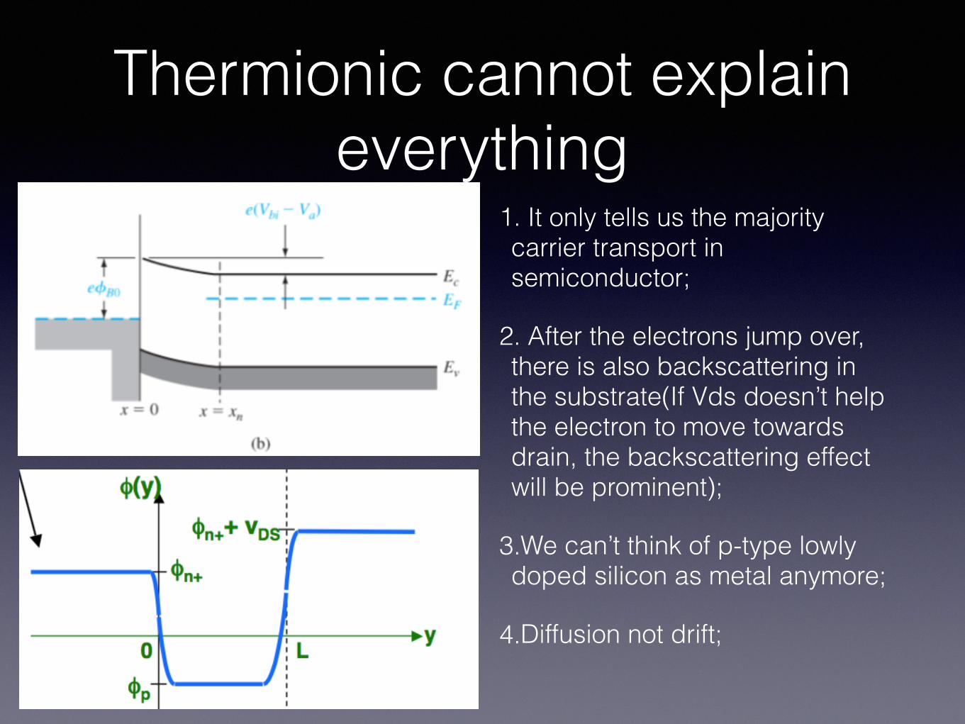
Thermionic cannot explain everything
1. It only tells us the majority carrier transport in semiconductor;
2. After the electrons jump over, there is also backscattering in the substrate(If Vds doesn’t help the electron to move towards drain, the backscattering effect will be prominent);
3.We can’t think of p-type lowly doped silicon as metal anymore;
4.Diffusion not drift;

The more complete theory
• 1. What happens before electrons jumps through the barrier? Thermionic or diffusion;
• 2. What happens once electrons jumps over? Drift or diffusion or ballistic;
• 3. After the electrons jump over, backscattering have to be considered too;

My partly-formed theory1. Something happens in the source(still a mystery);
2. Comparing to dc case, terahertz makes the fermi level in the source rise up or electron energy rise up;
3. Thus, electrons can pass the barrier even further beneath the surface in terahertz situation;
4.Electrons way beneath the surface will have better mobility(small Vgs have less capacity to draw electrons near surface) —>Does it help with backscattering???
5.Maybe for the electrons way beneath the surface, Vds will drop on the channel too instead of mostly on the depletion region, which will render less backscattering;
6. How about substrate doping profile? Increase Vds to find out?

So let’s discuss what happens or might happen in the source region!

In order to use circuit theory, real power(not reactive power) needs to be delivered between gate and source!!!
Basic concept for high frequency circuit

• Matching condition relates with loading condition; • We need to model the source and plug that here;
* Noting that this model is same to source region extension;
Method 1

Method 2• High Frequency model of the device between
source and gate(assume drain won’t matter):
ZL
C
RL
RS
• Since our operation frequency is way bigger than the fmax of 0.35u technology, the power into the transistor will be smaller than half.
• fmax;
L

Layout View•At least 130 Rsqr for source and drain outside connection;
•Antenna is closely connected to our detector;

Method 2• High Frequency model of the device between source and gate:
ZL
C
RL
RS
• RL mostly comes from source region resistance.
• C comes from intrinsic and extrinsic capacitance between gate and source.
• L comes from source region? Or the antenna? gate under nonquasi-static condition?
• To achieve the maximum power transmission, conjugate matching is a must;
L
• After matching, real power will drop on the source region;
How about Q?

0.2 0.3 0.4 0.5 0.6 0.7 0.8 0.9 1−0.5
0
0.5
1
1.5
2
2.5 x 10⁻⁶
T5 100% Power Normalized Ids vs VgsPreamp Gain=1.00e−05
Vds=3.00 V
Vgs (V)
Pow
er N
orm
aliz
ed Id
s
0.2 0.3 0.4 0.5 0.6 0.7 0.8 0.9 1−0.5
0
0.5
1
1.5
2
2.5 x 10⁻⁶
T5 Narrow Power Normalized Ids vs VgsPreamp Gain=2.00e−05
Vds=3.00 V
Vgs (V)
Pow
er N
orm
aliz
ed Id
s
0.2 0.3 0.4 0.5 0.6 0.7 0.8 0.9 1−0.5
0
0.5
1
1.5
2
2.5 x 10⁻⁶
T5 Wider Power Normalized Ids vs VgsPreamp Gain=5.00e−05
Vds=3.00 V
Vgs (V)
Pow
er N
orm
aliz
ed Id
s
• Center frequency barely changes while the capacitance follows the *1/2, *1, *2 relationship;
• Inductor needs to change accordingly so inductor effect can’t be coming from antenna;

Another interesting case to look at
0.2 0.3 0.4 0.5 0.6 0.7 0.8 0.9 1−0.5
0
0.5
1
1.5
2
2.5 x 10⁻⁶
T5 Tapper Power Normalized Ids vs VgsPreamp Gain=2.00e−05
Vds=3.00 V
Vgs (V)
Pow
er N
orm
aliz
ed Id
s
S D
G
• The gate doesn’t change at all but the result changes significantly; • Does this mean that the inductor is coming from source region?

Another direction• How about if gate is in high impedance mode and there
is no power injected? Only dc Vgs applied to gate.
• How about the power is directly injected into source due to its low impedance? Just look at the open end transmission line, the voltage and current still exist along the line;
Only problem will be where is the return path???

To test the gate independence, we need to disconnect the antenna from the gate!