the spin-dependent properties of silicon carbide/graphene
TRANSCRIPT

The Spin-Dependent Properties of SiliconCarbide/Graphene Nanoribbons Junctions withVacancy DefectsGolnaz Khanlar
University Campus2, University of GuilanSahar Izadi Vishkayi
Institute for Research in Fundamental Science (IPM)H. Rahimpour Soleimani ( [email protected] )
University of Guilan
Research Article
Keywords: Silicon carbide nanoribbons, Graphene nanoribbon, Spin-dependent thermoelectric, Vacancydefect, Half-metal, Density functional theory.
Posted Date: August 5th, 2021
DOI: https://doi.org/10.21203/rs.3.rs-754378/v1
License: This work is licensed under a Creative Commons Attribution 4.0 International License. Read Full License
Version of Record: A version of this preprint was published at Scienti�c Reports on December 1st, 2021.See the published version at https://doi.org/10.1038/s41598-021-03363-z.

The spin-dependent properties of silicon carbide/graphene nanoribbons
junctions with vacancy defects
Golnaz Khanlar 1, Sahar Izadi Vishkayi2 and H. Rahimpour Soleimani1,3
1Department of physics, University Campus2, University of Guilan, Rasht, Iran.
2School of Physics, Institute for Research in Fundamental Science (IPM), P. O. Box 19395‑5531, Tehran, Iran
3Computational Nanophysics Laboratory (CNL), Department of Physics, University of Guilan, P. O. Box
41335‑1914, Rasht, Iran. Email: [email protected]
Abstract: We have designed high-efficient spin-filtering junctions composed of graphene and silicon
carbide nanoribbons. We have calculated the spin and charge transport in the junction by non-equilibrium
Green’s function formalism combined with the density functional theory to find its spin-dependent
electrical conductance, thermal conductance and Seebeck coefficient. In addition, the effect of Si and C
atoms vacancies on the transport properties of the junction has been carefully investigated. The enhanced
spin-filtering is clearly observed due to the edge and vacancy effects. On the other hand, vacancy defects
increase the electrical and spin conductances of the junctions. The results show that the considered
junctions are half-metal with reduced thermal conductance which makes them a suitable spin-dependent
thermoelectric device. Our results predict the promising potential of the considered junctions for
application in spintronic devices.
Keywords: Silicon carbide nanoribbons; Graphene nanoribbon; Spin-dependent thermoelectric; Vacancy defect;
Half-metal; Density functional theory.
1. Introduction Finding and developing materials and devices with charge- and spin-dependent thermoelectric
performance are attractive for many theoretical and experimental researchers in nanoelectronics and
spintronics fields [1-5]. In fact, highly efficient charge-dependent thermoelectric materials can be used as
the energy convertor from a waste thermal energy to a useful electrical form. In particular, it is possible to
obtain a spin-dependent electrical potential by a thermal gradient in a device with a good spin-dependent
thermoelectric efficiency [6]. Low dimensional materials, consists of different junctions, are promising
candidates for this purpose because they showed high thermoelectric efficiency and also spin-filtering in
previous studies [2-4, 6, 7]. Here, we introduce a junction with a high-efficient spin-filtering which is
formed of silicon carbide (SiC) nanoribbon coupled to graphene nanoribbons. The spin-dependent
transport properties of the junction are computed by density functional theory (DFT) in combination with

Green function formalism. We have obtained the thermoelectric properties of the junction in the linear
response regime [8].
The combination of Silicon (Si) and Carbon (C) atoms in silicon carbide has caused the emergence of
unique properties which attracted many researchers [9-11]. SiC nanoribbons have been synthesized via
catalyst-free growth method which has honeycomb- graphene-like- structures [12]. There are many
numbers of research on SiC nanoribbons that show their interesting properties [10, 12-14]. So, it can be a
basic block for our investigation due to its unique properties. On the other hand, graphene is a highly
flexible semi-metal with promising mechanical strength [15, 16] which can be coupled to other
nanomaterials as the electrodes [17, 18]. The graphene nanoribbon (GNR), has been proposed for the
interconnect application. It indicated that both metallic and semiconducting GNRs provide lower
resistivity than those of Cu and single-walled CNT (SWCNT) bundle [19]. The zigzag graphene
nanoribbon is known as a popular material for spintronic investigation [20-23]. Because of the strong
interface bonding between graphene and SiC [24], we have selected zigzag GNRs as the electrodes which
are coupled to the SiC ribbon.
An ideal thermoelectric device works very well if its heat conductivity is poor [25, 26]. To obtain a
suitable material for thermoelectric applications, it must have high electrical conductivity and the thermal
conductivity should also be kept as low as possible to prevent heat loss. It is expected that in our
considered junction, composed of SiC nanoribbon as the central region and GNRs as the electrodes, the
phonon thermal conductance is small because of the reduction of phonon movement in inhomogeneous
structures [27], so it can be a suitable suggested thermoelectric device. On the other hand, the zigzag
edges of GNR and SiC induce spin-dependent electrical properties in the device [13] which make it a
good spin-dependent thermoelectric device.
It is obvious that vacancy defects are created in the growth process of the structures. The vacancy
defects affect the electronic and magnetic properties of SiC [14, 28]. On the other hand, the vacancy
defects reduce the thermal conductance of nanoribbons [29] therefore we have considered the effect of
SiC vacancy defect on the thermoelectric properties of the junction. Our results show that the Si- and C-
defected SiC nanoribbons have a significant effect on the thermoelectric properties of the considered
junction. Furthermore, there is a good spin-filtering in the junction which shows its potential for use as a
spintronic device.
In the following, the computational methods are presented in section 2 and the simulation results and
discussions are given in section 3. Finally, in section 4, a brief of the results is reported.

2. Computational methods
The considered junction is shown in Fig.1, which is composed of a silicon carbide nanoribbon (SiCNR)
coupled to graphene nanoribbons (GNRs) in two sides as the electrodes. The GNRs and SiCNR with
zigzag edges are considered to have extremely high magnetization at the edges. The length of central area
is 9.778 (�̇�) and its width is 14.260 (�̇�). The size of central region is enough small to have ballistic
transport in the junction. All the calculations for optimization of the structure had been done by SIESTA
DFT-based package [30]. The transport properties of considered structures are calculated by Green
function formalism which is implanted in TRANSIESTA package [31]. We used generalized gradient
approximation (GGA) [32] to describe the exchange-correlation functional. The converged cutoff energy
for the high-level energy of wave function is 80 Hartree.
Figure 1.The optimized geometry of the silicon carbide nanoribbon between the GNRs. Carbon (silicon) atoms are represented
by gray (yellow) circles.
The thermoelectric efficiency of a system is obtained by [6, 8]
𝑍𝑇 = 𝐺𝑒𝑆𝑐2𝑇(𝜅𝑒↑+𝜅𝑒↓+𝜅𝑝ℎ), (1) where Ge is the electrical conductance, 𝑆𝐶 states as the charge Seebeck coefficient, T is the absolute
temperature of the junction. 𝜅e↑, κe↓ and κph are the spin-up and spin-down electrons thermal
conductances and phonons thermal conductance, respectively. The charge Seebeck coefficient is given by 𝑆𝐶 = − 12|𝑒|𝑇 (𝐿1↑𝐿0↑ + 𝐿1↓𝐿0↓) while the spin Seebeck coefficient is the difference between spin-up and spin-
down Seebeck coefficients, 𝑆𝑠 = − 12|𝑒|𝑇 (𝐿1↑𝐿0↑ − 𝐿1↓𝐿0↓). The electrical conductance and the electron thermal
conductance are equal to 𝐺𝑒 = 𝑒2𝐿0 and 𝜅𝑒 = 1 𝑇 [𝐿2 − 𝐿12𝐿0] where 𝐿𝑛 = 1ℏ ∫ 𝑑𝜀 𝑇(𝜀) (− 𝜕𝑓𝜕𝜀) (𝜀 − 𝜇)𝑛. In
this equation, 𝑓(𝜀) is the Fermi–Dirac distribution function of the left or right electrodes and 𝜇 is the
chemical potential of the electrode. The spin and energy dependent transmission coefficient is given by

𝑇𝜎(𝜀) = 𝑇𝑟[𝛾𝐿𝜎(𝜀)G𝜎𝑅(𝜀)𝛾𝑅𝜎(𝜀)G𝜎𝐴(𝜀)], where 𝛾𝐿𝜎(𝛾𝑅𝜎) describes the broadening function of the energy
levels due to coupling of the left (right) electrode to the central region and G𝜎𝑅(𝜀) (G𝜎𝐴(𝜀)) expresses the
retarded (advanced) Green function [6] with spin σ.
The phonon thermal conductance is given by [33]
𝜅𝑝ℎ = ħ22𝜋𝑘𝐵𝑇2 ∫ 𝑑𝜔 𝜔2∞0 𝑇𝑝ℎ(𝜔) 𝑒 ħ𝜔𝑘𝐵𝑇(𝑒 ħ𝜔𝑘𝐵𝑇−1)2, (2)
where ħ𝜔 is the phonon energy and 𝑇𝑝ℎ(𝜔) is the phonon transmission coefficient [33] calculated by
Green function formalism in a way similar to the calculation of electron transmission coefficient.
However, to find 𝑇𝑝ℎ, we used reactive force field classical potential [34] which makes the force constant
matrices of the electrodes and the central region.
3. Result and discussions
In this article, the edges of GNRs electrodes are considered in two spin configurations; parallel (P) and
anti-parallel (AP), in which the spin orientations of carbon atoms at the edges of left and right electrodes
are parallel and anti-parallel, respectively. In the SiCNR coupled to the electrodes with P configuration,
the spin-up and spin-down transmission coefficients (𝑇𝑒𝑙↑ 𝑎𝑛𝑑 𝑇𝑒𝑙↓) of carriers are obviously separated
(see Fig. 2 (a)). In the energy range of 0.05-0.25 eV, there is a small transmission for carriers with spin-up
orientation, while spin-down carriers are not transmitted through the channel so we can consider that the
device acts like a half-metal. It is interesting that half-metallicity is very intense in the AP spin-
configuration of the electrodes because 𝑇𝑒𝑙↓ is more than 𝑇𝑒𝑙↑ around the Fermi energy and the spin-
splitting is completely observed in Fig. 2 (b).
Figure 2.The spin-up (red lines) and spin-down (blue lines) electron transmission coefficients of SiCNR in (a) P and (b) AP
configurations. The insets show the spin density diagram of the junction. Red (blue) color represents the spin-up (-down) density
and the mean values of spin densities are given in the scroll bar at the bottom of the diagrams.

In General, the electron transmission of spin-up and spin-down carriers are the same in common AP
systems, but here a strong spin separation is observed due to the geometrical antisymmetric which exists
in the central region. There are carbon (silicon) atoms at the top (bottom) edge of SiCNR. In the insets of
Fig.2 (a) and (b), it is obviously observed that the spin density of carbon atoms is more than silicon one in
the central region of the junctions. Therefore, spatial separation of spin density is achieved. In P
configuration, the spin-down energy states of the central region cannot transfer through the spin-up carrier
states of the electrodes but in AP configuration one of the electrodes has spin-down energy states, so the
spin-down electrons can transfer through the spin-down states of the junction and a maximum of
transmission at zero energy is observed for the spin-down carriers.
Figure 3. The spin-dependent electron transmission coefficients of (a) and (b) Si-defected SiCNRs in P and AP configurations
and (c) and (d) C-defected SiCNRs in P and AP configurations, respectively. The insets show the corresponding spin density
diagram of the junctions. Red (blue) color represents the spin-up (-down) density and the mean values of spin densities are as the
same as Fig.2.
Vacancy defects have an important role on the electrical and magnetic properties of structures. Here,
we have considered the SiCNRs with vacancies at the channel. The vacancy leads to the increment of the
spin density by electron injection because of the appearance of dangling bonds. In the Si-defected SiC,
which a Si atom is eliminated at the center of the channel, the transmission coefficient is increased around
the Fermi level; however, the transmission coefficient of spin-down carries is more than spin-up ones
when the electrodes are in P configuration (see Fig. 3 (a)), while in the AP configuration, Fig. 3 (b), 𝑇𝑒𝑙↑

is more than 𝑇𝑒𝑙↓ near the zero energy. In the P configuration of electrodes, the spin density diagram
shows that the elimination of a Si atom changes the spin density of the pristine device (in comparison
with the insets of Fig.2 (a) and 3 (a)). The spin density has been moved to the central region (on the
neighbors of the vacant atom) while it was focused on the upper edge of the pristine SiCNR. It is
observed that the spin density is different on the nearest-neighbor carbon atoms at the left and right sides
of the vacant atom. This kind of spin induction is due to extra electrons injection by the vacant atom. In
the Ap configuration, the spin density diagram is changed at the edge of SiCNR and half of the carbon
atoms at the edge of SiCNR have spin-down density. The carbon on the right hand of vacant atom is
coupled ferromagnetically to the right electrode and two other nearest-neighbor carbon atoms (at the left
and bottom of the vacant atom) are coupled anti-ferromagnetically to the first carbon atom in both P and
AP configurations. In P configuration, the spin densities of the nearest-neighbour atoms of vacancy are
vice versa of the spin densities of the same atoms at AP configuration. In other words, the sign of their
spins comes from the interaction of the channel with the right electrode. As a consequence, in P
configuration, two carbon atoms with spin-down electrons, around the vacancy, induce more spin-down
transmission channels in the junction in comparison with the perfect SiCNR which can be observed in the
transmission coefficient graph around the zero energy. on the other hand, in AP configuration, the
mentioned carbon atoms have spin-up carriers, so 𝑇𝑒𝑙↑ should be increased in the zero energy.
To find a comprehensive insight into the vacancy’s effects on the properties of the junction, we have
also considered the elimination of C atoms at the middle of SiCNR and named it by C-defected SiC. The
transmission coefficient of C-defected SiC is shown in Fig. 3 (c) and (d) for P and AP configurations,
respectively. By the elimination of a C atom at the center of the channel, its Si neighbors get dangling
bonds that lead to injection of spin-density on them, but the spin-density of silicon atom is less than
carbon atoms, therefore the edge carbon atoms are also the main source of spin density at the central
region of the considered structures in both P and AP configurations. So, we expect to see a small
deviation from the pristine configurations for transmission coefficients. The spin-up transmission is
increased around the zero energy for P configuration. On the other hand, in AP configuration, the spin-
down transmission is decreased around zero energy. Half-metallicity is also conserved in AP
configuration of C-defected SiC.
The spin-filtering is observed in the transmission coefficients and spin-density diagrams of the
considered junctions. Therefore, the spin-dependent thermoelectric properties of the junctions may be
interesting for researchers. In this part, we explore the thermoelectric properties of the considered
junctions. In Fig. 4 (a) and (b), the electrical conductances of the considered junctions are shown for P
and AP configurations, respectively. It is obviously observed that the electrical conductance is increased
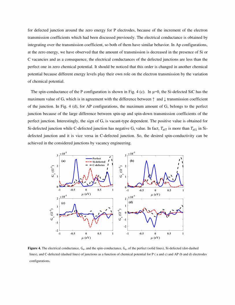
for defected junction around the zero energy for P electrodes, because of the increment of the electron
transmission coefficients which had been discussed previously. The electrical conductance is obtained by
integrating over the transmission coefficient, so both of them have similar behavior. In Ap configurations,
at the zero energy, we have observed that the amount of transmission is decreased in the presence of Si or
C vacancies and as a consequence, the electrical conductances of the defected junctions are less than the
perfect one in zero chemical potential. It should be noticed that this order is changed in another chemical
potential because different energy levels play their own role on the electron transmission by the variation
of chemical potential.
The spin-conductance of the P configuration is shown in Fig. 4 (c). In μ=0, the Si-defected SiC has the
maximum value of Gs which is in agreement with the difference between ↑ and ↓ transmission coefficient
of the junction. In Fig. 4 (d), for AP configurations, the maximum amount of Gs belongs to the perfect
junction because of the large difference between spin-up and spin-down transmission coefficients of the
perfect junction. Interestingly, the sign of Gs is vacant-type dependent. The positive value is obtained for
Si-defected junction while C-defected junction has negative Gs value. In fact, 𝑇𝑒𝑙↑ is more than 𝑇𝑒𝑙↓ in Si-
defected junction and it is vice versa in C-defected junction. So, the desired spin-conductivity can be
achieved in the considered junctions by vacancy engineering.
Figure 4. The electrical conductance, Ge, and the spin-conductance, Gs, of the perfect (solid lines), Si-defected (dot-dashed
lines), and C-defected (dashed lines) of junctions as a function of chemical potential for P ( a and c) and AP (b and d) electrodes
configurations.
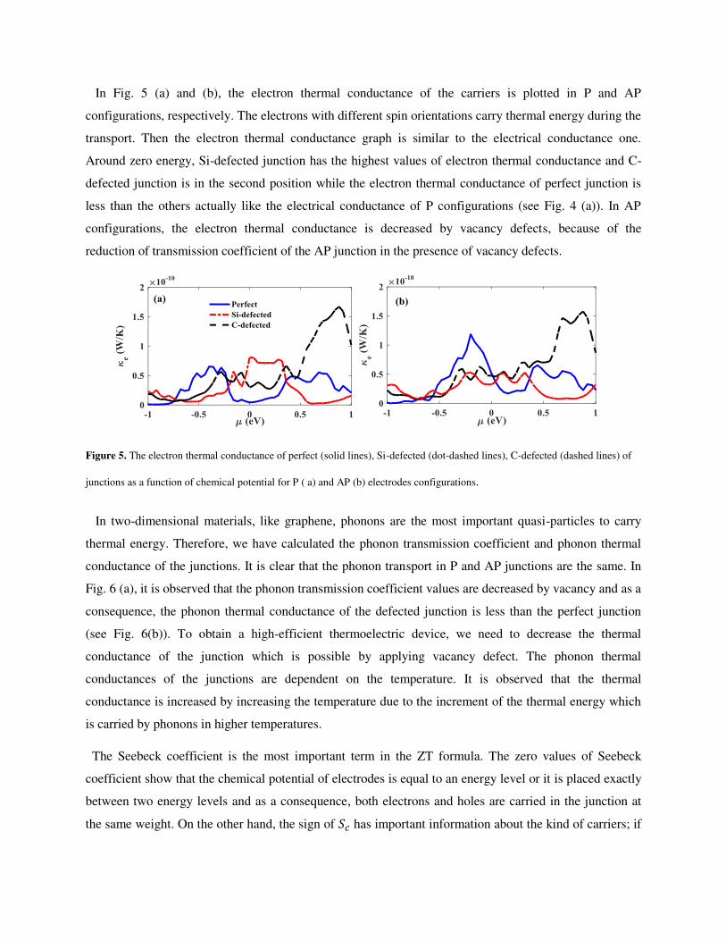
In Fig. 5 (a) and (b), the electron thermal conductance of the carriers is plotted in P and AP
configurations, respectively. The electrons with different spin orientations carry thermal energy during the
transport. Then the electron thermal conductance graph is similar to the electrical conductance one.
Around zero energy, Si-defected junction has the highest values of electron thermal conductance and C-
defected junction is in the second position while the electron thermal conductance of perfect junction is
less than the others actually like the electrical conductance of P configurations (see Fig. 4 (a)). In AP
configurations, the electron thermal conductance is decreased by vacancy defects, because of the
reduction of transmission coefficient of the AP junction in the presence of vacancy defects.
Figure 5. The electron thermal conductance of perfect (solid lines), Si-defected (dot-dashed lines), C-defected (dashed lines) of
junctions as a function of chemical potential for P ( a) and AP (b) electrodes configurations.
In two-dimensional materials, like graphene, phonons are the most important quasi-particles to carry
thermal energy. Therefore, we have calculated the phonon transmission coefficient and phonon thermal
conductance of the junctions. It is clear that the phonon transport in P and AP junctions are the same. In
Fig. 6 (a), it is observed that the phonon transmission coefficient values are decreased by vacancy and as a
consequence, the phonon thermal conductance of the defected junction is less than the perfect junction
(see Fig. 6(b)). To obtain a high-efficient thermoelectric device, we need to decrease the thermal
conductance of the junction which is possible by applying vacancy defect. The phonon thermal
conductances of the junctions are dependent on the temperature. It is observed that the thermal
conductance is increased by increasing the temperature due to the increment of the thermal energy which
is carried by phonons in higher temperatures.
The Seebeck coefficient is the most important term in the ZT formula. The zero values of Seebeck
coefficient show that the chemical potential of electrodes is equal to an energy level or it is placed exactly
between two energy levels and as a consequence, both electrons and holes are carried in the junction at
the same weight. On the other hand, the sign of 𝑆𝑐 has important information about the kind of carriers; if

𝑆𝑐 > 0, the electrons are the main carriers passed through the junction while holes are responsible for the
transport when the values of charge Seebeck coefficients are negative.
Figure 6. (a) The phonon transmission coefficient and (b) the phonon thermal conductance of the perfect (blue solid lines), the
Si-defected (red dot-dashed lines) and the C-defected (black dashed lines) of junctions as a function of temperature.
Figure 7. The charge Seebeck coefficient, Sc, and the spin Seeebeck coefficient, Ss, of the perfect (solid lines), Si-defected (dot-
dashed lines), C-defected (dashed lines) junctions as a function of chemical potential for P ( a and c) and AP (b and d) electrodes
configurations.

In Fig. 7 (a) and (b), the charge Seebeck coefficient of the junctions are given in P and AP
configurations. In P configuration, the positive 𝑆𝑐 value is achieved for the perfect junction at zero
chemical potential, which shows the electrons are the main carriers. By vacancy defect, the carriers are
changed to holes and the charge spin Seebeck coefficient is negative for both Si-defected and C-defected
junction in P configuration. It is clearly in agreement with the transmission coefficient peaks which
placed in negative energy near to zero energy (see Fig. 3). At zero chemical potential, 𝑆𝑐 is less than zero
for all the junctions in AP configurations (Fig. 7 (b)), so holes are the main carriers passed through the
junctions. By variation of the chemical potential, different energy levels enter in the transport process
then electrons or holes can be the charge carriers in the junction which make positive or negative charge
Seebeck coefficient.
The difference between 𝑆𝑐↑ and 𝑆𝑐↓ gives the spin Seebeck coefficient that shows the junction ability for
inducing a spin accumulation with a temperature gradient [6]. The values of the spin-dependent Seebeck
coefficient is dependent on the strength of making spin accumulation in the junction while the negative
(positive) sign shows that the spin-down (spin-up) Seebeck coefficient is more than the spin-up (spin-
down) one. In Fig. 7 (c) and (d), the spin Seebeck coefficient of the P and AP junctions are shown. It is
demonstrated that 𝑆𝑠 has an oscillating behavior as a function of chemical potential which is due to the
entering of different spin states of different energy levels in the transport mechanisms. In zero chemical
potential, there is a small difference between 𝑆𝑐↑ and 𝑆𝑐↓ of perfect P junction, which makes a small spin
Seebeck coefficient. By applying vacancy defects, this difference amount is increased especially for C-
defected junction. In AP configuration, despite the perfect junction has a positive spin Seebeck
coefficient, the junctions with vacancies have negative values at 𝜇 = 0. This means that the spin
accumulation type is changed by vacancy defect.
By increasing the electrical conductance and Seebeck coefficient and decreasing the thermal
conductance, the thermoelectric efficiency of the device is increased. In Fig. 8 (a), 𝑍𝑇𝑐 values of the
perfect junction are ignorable around zero chemical potential because of vanishing the electrical
conductance while applying vacancy defects increases its values. In 𝜇 = +0.04 𝑒𝑉 and 𝜇 = −0.04 𝑒𝑉,
the 𝑍𝑇𝑐 values of C-defected and Si-defected junctions are around 0.05. By variation of the chemical
potential, thermoelectric efficiencies of the defected junctions are increased up to 𝑍𝑇𝑐 = 0.1 which is a
result of the increment of the Seebeck coefficient. In the junctions with AP configurations, around zero
chemical potential, the perfect junction has non-zero 𝑍𝑇𝑐 values because of having the strong
transmission channel in zero energy, and by changing the chemical potential, it also reaches 𝑍𝑇𝑐 = 0.2
(see Fig. 8 (b)). In general, the C-defected junction is a better thermoelectric efficient device in
comparison with the Si-defected junction because of its reduced phonon thermal conductance.

Figure 8. The charge thermoelectric efficiency, ZTc, and the spin thermoelectric efficiency, ZTs, of the perfect (solid lines), Si-
defected (dot-dashed lines) and C-defected (lines with diamonds) junctions as a function of chemical potential for P ( a and c)
and AP (b and d) electrodes configurations.
In Fig. 8 (c) and (d), it is observed that the values of 𝑍𝑇𝑠 are increased by vacancy defect for both P and
AP configurations, so the considered defects can induce a spin-dependent electrical potential difference in
the junctions. Therefore, these junctions can be a promising candidate for the application in spintronics
and logic memory devices. In fact, it is possible to make a desired electrical potential difference with a
determined spin orientation, by engineering the chemical potential and vacancy defect type in the
junction. For example, In the P configuration, at 𝜇 = −0.36 𝑒𝑉, the amount of 𝑍𝑇𝑠 is equal to +0.10
which shows the accumulation of spin-down carriers in the junction. On the other hand, 𝑍𝑇𝑠 is equal to -
0.18 at 𝜇 = +0.36 𝑒𝑉 which shows that the junction is an efficient device for the creation of spin-down
electrical potential difference. In AP configuration, the C-defected junction has the best spin-
thermoelectric efficiency, because its 𝑍𝑇𝑠 is about +0.14 at 𝜇 = −0. −35 𝑒𝑉 while it is equal to -0.16 at 𝜇 = +0.04 𝑒𝑉. Therefore, a switchable spin-dependent electrical potential is obtained by changing the
chemical potential in the C-defected junction.

4. Conclusion
Here, a junction of SiC nanoribbon coupled to the zigzag GNRs is investigated in both parallel and
antiparallel spin configurations of zigzag GNRs edges. The thermoelectric properties of the junction are
calculated by density functional theory and Green’s function technique. Spin-polarized transmission
coefficients are obtained for both P and AP configurations while a perfect half-metallic behavior is
observed in the AP configuration due to the asymmetric edges of SiC in the central region. The Si- and C-
defected SiC nanoribbons are also considered as the central region. The spin density of the junction is
dependent on the edge and the type of vacancy defects in the junction. The results show that it is possible
to engineer the sign of spin-conductance by the type of vacancy defects. On the other hand, the vacancy
defects leading to the reduction of phonon thermal conductance of the junction. In Seebeck coefficient
analysis, it is demonstrated that the kind of charge carriers can be tuned by the type of vacancy defects.
The spin Seebeck coefficient amount and sign are changed by the vacancy in the SiC region and the edge
configurations of the GNRs. Our results suggest that the considered junctions can act as suitable spin
filters in spintronics and logic memory devices. We have also predicted a switchable spin-dependent
electrical potential in the C-defected junction with an acceptable spin thermoelectric efficiency.
References
[1] W. Lin, M. Hehn, L. Chaput, B. Negulescu, S. Andrieu, F. Montaigne, S. Mangin, “Giant spin-
dependent thermoelectric effect in magnetic tunnel junctions”, Nature Commun., 3 (2012) 744.
[2] F. Ildarabadi, R. Farghadan, “Spin-thermoelectric transport in nonuniform strained zigzag graphene
nanoribbons”, Phys. Rev. B, 103 (2021) 115424.
[3] L. Zhu, B. Li, H. Ma, M. Qian, K. Yao, “Electrical-field tuned thermoelectric performance of
graphene nanoribbon with sawtooth edges”, Nanotech., 30 (2019) 445204.
[4] M. Zeng, W. Huang. G. Liang, “Spin-dependent thermoelectric effects in graphene-based spin
valves”, Nanoscale, 5 (2013) 200.
[5] L. Zhu, F. Zou, G. Gao, K. Yao, “Spin-dependent thermoelectric effects in Fe-C6 doped monolayer
MoS2”, Sci. Rep., 7 (2017) 497.
[6] D. D. Wu, H. H. Fu, Q. B. Liu, R. Wu, “How to realize the spin-Seebeck effect with a high spin figure
of merit in magnetic boron–nitrogen nanoribbon and nanotube structures?”, J. Mater. Chem. C, 6 (2018)
10603.
[7] M. Wierzbicki,R. Swirkowicz, J. Barnaś, “Giant spin thermoelectric efficiency in ferromagnetic graphene nanoribbons with antidots”, Phys. Rev. B, 88 (2013) 235434.
[8] L. D. Hicks, M. S. Dresselhaus, Phys. Rev. B: Condens. Matter, 47 (1993) 12727.
[9] S. Choudhary, S. Jalu, “First-principles study of spin transport in Fe–SiCNT–Fe magnetic tunnel
junction”, Phys. Lett. A, 379 (2015) 1661.
[10] K. Zberecki, R. Swirkowicz, M. Wierzbicki, J. Barnas, “Spin effects in thermoelectric phenomena in SiC nanoribbons”, Phys. Chem. Chem. Phys, 17 (2015), 1925.

[11] A. Gali, “Ab initio study of nitrogen and boron substitutional impurities in single-wall SiC
nanotubes”, Phys. Rev B, 73 (2006) 245415.
[12] H. Zhang, W. Ding, K. He, M. Li, “Synthesis and Characterization of Crystalline Silicon Carbide
Nanoribbons”, Nanoscale Res. Lett. 5 (2010) 1264.
[13] Y. Zhou, X. Zhuge, K. Luo, P. An, S. Du, “The defect impacts of zigzag SiC nanoribbons in the spin devices”, Phys. Lett. A, 384 (2020) 126852.
[14] J. M. Morbec, G. Rahman, “Role of vacancies in the magnetic and electronic properties of SiC
nanoribbons: an ab initio study”, Phys. Rev. B, 87 (2013)115428.
[15] T. H. Hana, H. Kim, S. J. Kwon, T. W. Lee, “Graphene-based flexible electronic devices”, Mater.
Sci. Eng.: R: Rep., 118 (2017) 1.
[16] C. Vallés, J. D. NúñezAna, M. B. Wolfgang, K. Maser, “Flexible conductive graphene paper obtained by direct and gentle annealing of graphene oxide paper”, Carbon, 50 (2012) 835.
[17] B . Zhou , B . Zhou , Y . Zeng , G . Zhou , M . Duan, “Electronic and thermoelectric transport properties for an armchair graphene–silicene–graphene heterojunction modulated by external field”, Phys.
Lett. A, 380 (2016) 2984.
[18] J. Li, B. Wang, F. Xu, Y. Wei, J. Wang, “Spin-dependent Seebeck effects in graphene-based
molecular junctions”, Phys. Rev. B, 93 (2016)195426.
[19] A. Naeemi, J. D. Meindl, “Compact physics-based circuit models for graphene nanoribbon
interconnects”, IEEE Trans. Electron Dev., 56 (2009) 9.
[20] J. Yu, W. Guo. “A New Paradigm to Half-Metallicity in Graphene Nanoribbons” Phys. Chem. Lett. 4
(2013) 951.
[21] S. G. Cheng, “Spin thermopower and thermoconductance in a ferromagnetic graphene nanoribbon”, J. Phys.: Cond. Matt., 24 (2012) 385302.
[22] Y. T. Zhang, H. Jiang, Q. F. Sun, X. C. Xie, “Spin polarization and giant magnetoresistance effect
induced by magnetization in zigzag graphene nanoribbons”, Phys. Rev. B, 81 (2010) 165404.
[23] L. Zhang, J. Chen, L. Zhang, F. Xu, L. Xia, S. Jia, “Gate controllable optical spin current generation in zigzag graphene nanoribbon”, Carbon, 173 (2021) 565.
[24] J. B. Wallace, D. Chen, L. Shao, “Carbon Displacement-Induced Single Carbon Atomic Chain
Formation and its Effects on Sliding of SiC Fibers in SiC/graphene/SiC Composite”, Mater. Res. Lett., 4
(2016) 55.
[25] Y. Hu, T. Yang, D. Li, G. Ding, C. Dun, D. Wu, X. Wang, “Origins of Minimized Lattice Thermal Conductivity and Enhanced Thermoelectric Performance in WS2/WSe2 Lateral Superlattice”, ACS
Omega, 6 (2021) 7879.
[26] A. Ovchinnikov, S. Chanakian, A. Zevalkink, S. Bobev, “Ultralow Thermal Conductivity and High
Thermopower in a New Family of Zintl Antimonides Ca10MSb9 (M = Ga, In, Mn, Zn) with Complex
Structures and Heavy Disorder”, Chem. Mater. (2021), https://doi.org/10.1021/acs.chemmater.0c04940
[27] S. I. Vishkayi, M. B. Tagani, H. R. Soleimani, “Enhancement of thermoelectric efficiency by embedding hexagonal boron-nitride cells in zigzag graphene nanoribbons”, J. Phys. D: Appl. Phys. 48
(2015) 235304.
[28] E. Bekaroglu, M. Topsakal, S. Cahangirov, and S. Ciraci, “A First-Principles Study of Defects and
adatoms in Silicon Carbide Honeycomb Structures”, Phys. Rev. B, 81 (2010) 075433.
[29] S. I. Vishkayi, H. R. Soleimani, “The influence of edge defects on the electrical and thermal transport of graphene nanoribbons”, Physica E, 74 (2015)363.

[30] J. M. Soler, E. Artacho, J. D. Gale, A. Garca, J. Junquera, P. Ordejn, D. Snchez-Portal, “The siesta method for ab initio order- n materials simulation”, J. Phys.: Cond. Matt., 14 (2002) 2745.
[31] M. Brandbyge, J. L. Mozos, P. Ordejón, J. Taylor, K. Stokbro, “Density-functional method for
nonequilibrium electron transport”, Phys. Rev. B, 65 (2002) 165401.
[32] J. P. Perdew, J. A. Chevary, S. H. Vosko, K. A. Jackson, M. R. Pederson, D. J. Singh, C. Fiolhais,
“Atoms, molecules, solids, and surfaces: Applications of the generalized gradient approximation for
exchange and correlation”, Phys. Rev B, 48 (1993) 4978.
[33] N. Mingo, L. Yang, “Phonon transport in nanowires coated with an amorphous material: An atomistic Green’s function approach” Phys. Rev. B, 68 (2003) 245406.
[34] Oliver Böhm, AQcomputare GmbH, “SiCNH parameter set”, 2015.