the random pulse width modulation technique for vsi for
TRANSCRIPT

The Random Pulse Width Modulation Technique for
VSI for Harmonic-Spectrum Spreading Noise
Cancellation
P. Booma Devi*, M.Karthikeyan**, P. Vijayarajan ***, C. Bharatiraja****, * Department of Electrical and Electronics Engg., SSM Institute of Engineering & Technology, Dindigul, India.
** Department of Electrical and Electronics Engg., University College of Engineering, Pattukkottai, India
*** Assistant Professor, Department of Electrical and Electronics Engg., University college of Engineering, BIT
Campus, Tiruchirappalli, India.
****Department of Electrical and Electronics Engg., SRM Institute of Science and Technology, Chennai.
Abstract – The Power electronics switch-based
voltage source inverter (VSI) based induction motor
drive are budding in almost all the industries due to
their controllability. The pulse switch modulation
(PWM) is a main coin for the VSI performance and
liability to control the drive. However the PWMs are
not intellectual for reducing the high frequencies
spectrum noises. The PWM is responsible for give
more control degree of freedom and les harmonics
spectrum noises. In the paper, the random PWM
(PRWM) scheme is developed for VSI connected indication motor and study on noise reduction of the
line voltage. The proposed RPWM method is capable
to build a gap in the line voltage spectrum at choosy
frequency in human hearing range. The proposed
RPWM is developed for 1 kHz to 4 kHz carrier
frequency range and voltage noise harmonic spectrum
is studied for both MATBLAB based software
simulation and low scale experimentation for RL
using PIC microcontroller platform. The Analysis,
simulation and experimentation validating the
proposed RPWM.
Keywords: VSI, RPWM, Random SVPWM, voltage
noise harmonic spectrum, Acoustic noise, three phase
voltage source inverters.
1. Introduction
The voltage source inverter (VSI) based high and
medium power induction motor drive are growing in
almost all the industries such as shipping and
automotive industry [1-2]. Similar to VSI, multilevel
inverter (MLI) has given lot of interest in power
electronic application [3-8] These drives are mainly
focusing on their variable speed-torque characteristics
and continuous operation profile. This variable speed
drives also concentrating acoustic noise reductions
[9]. These acoustic noise present in the voltage and current waveform due to high frequency supply
current harmonics, which also causes the vibration on
the drive system. When system operated in low speed
range this vibration is very high and affecting drive
performance. Hence the reduction of high frequency
noise is much attractive in the research community in
the academic and industry. The reduction of noise on
the VSI drive is mainly done through pulse width
modulation (PWM) techniques.Different PWM
methods are used in a mixture of ASD claims. The
lower switching frequency presents the acoustic noise
amid low losses and higher switching frequency
amplifies the losses in the inverter, however can
reduce the acoustic hitch. The noteworthy
enhancement in the acoustic as well as
electromagnetic noise in random PWM (RPWM) have been developed in several publications for keeping
low-audible noise profile with low switching
frequency disturbances simultaneously. Many
research papers are published in PWM modification,
which is basically altering existing PWM pattern [10].
These PWM techniques are called as RPWM. The
RPWM is has developed for VSI drive to mitigate the
high frequency [11]. The innovative RPWM
technique to avoid whistling along with EMI noise
reductions [12]. The quality of output waveforms as
well as the performance can be enhanced based on the
PWM theory. Recently fixed switching frequency SVPWM methods are used in three-phase inverter
[12-13] in addition with harmonics eliminations. The
author in [14-15] examines several brands of RPWM
methods from observation of harmonic spreading and
efficiency. There are two categories of RPWM: one
has a fixed switching frequency and the other is based
on the variable switching frequency. In RPWM based
techniques, the power of noise is spread in wide
choice of frequency domain which increases the
voltage acoustic noise and vibration [16-18]. As a
result, when RPWM is used, switching of power converters is required to be controlled in a way that
the noise is reduced at desired range of frequency
(resonant frequency of load).
The RPWM technique is presented in [19,20] for
improving acoustic and EMI characteristics. The
methods based on regulating the duration of the Null
vector switching or adjusting the all three phase
corresponding pulse positions switching period are
introduced in [18]. The Pedersen et al. [21-
22]attended an RPWM varying±1kHz spared range.
The reduced noise power spectrum in a particular
interval in frequency domain by eliminate in the
selective range of switching frequencies. Beside with
providing a space in the frequency spectrum, this
technique leads to add to in peak of power spectrum density. Along with noise reductions the VSI fed
drives are required to maintains the fundamental
voltage, which give a ensure the wider range of speed
and power characteristics. With this aim, many
researches are reported on SVPWM to improve the
fundamental voltage improvement [26,26]. Authors in
[27], has proposed excellent PWM methods for
improving the drive performance with common mode
voltage eliminations. Based on the above mentioned
discussions, the variable speed drive application VSIs
are is need to satisfy to provide a higher fundamental
voltage with harmonic-spectrum spreading noise cancellation. Besides, PWM modification online
carrier frequency adjustment possibilities in the field
of digital control using by micro-controller, complex
programmable logic devices, field programmable gate
array (FPGA), digital signal processor (DSP), and
application specific integrated circuit (ASIC)
technologies. Among all RPWM techniques [25,31]
with online carrier modification handling is highly
possible through FPGA since it has flexibility for
online programming solution and the high efficiency
architecture with a high speed and, high integration density. The FPGA technology offers
reprogrammable SOC environment for particular
applications [32], However the FPGA based
implementation demands high which is not desirable.
Though microcontroller is not better candidate for
wide range noise spectrum cancellation in on line
carrier frequency injection/ adjustments. However,
with respect to particular spread THD noise can be
eliminated 8 bit PIC microcontroller is a preeminent
entrant.
The paper proposes the PWM with merging of
RPWM with space vector PWM. In the proposed PWM the carrier frequency (fc) is sampled and added
and subtracted with switching frequency. The carrier
frequency, fc are altered by using fc adjustment along
with added, and subtracted fashion. The 8-bit
microcontroller is used for implementing the proposed
PWM. The simulation and low cost experimentation
is proving the pros of the proposed PWM.
2. REVIEW OF THE CONVENTIONAL TWO-
LEVEL VOLATGE SOURCE INVERTER
AND RANDOM PWM
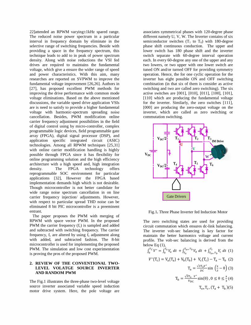
The Fig.1 illustrates the three-phase two-level voltage
source inverter associated variable speed induction
motor drive system. Here, the pole voltage are
associates symmetrical phases with 120-degree phase
different namely U, V, W. The Inverter contains of six
semiconductor switches (T1 to T6) with 180-degree
phase shift continuous conduction. The upper and
lower switch has 180 phase shift and the inverter
switch separate with 60-degree interval operation each. In every 60-degree any one of the upper and any
two lowers, or two upper with one lower switch are
tuned ON and/or turned OFF for providing symmetry
operation. Hence, the for one cyclic operation for the
inverter has eight possible ON and OFF switching
combination (in that six of them is consider as active
switching and two are called zero switching). The six
active switches are [001], [010], [011], [100], [101],
[110] which are producing the fundamental voltage
for the inverter. Similarly, the zero switches [111],
[000] are producing the zero-output voltage on the
inverter, which are called as zero switching or commutation switching.
VDC/2 T1
UV
W
IM DriveT2 T3
T4 T5 T6 VDC/2
VDC
Gate Drivers
Fig.1. Three Phase Inverter fed Induction Motor
The zero switching states are used for providing
circuit commutation which ensures dc-link balancing.
The inverter volt-sec balancing is key factor for maintain the better harmonics voltage and current
profile. The volt-sec balancing is derived from the
below Eq (1),
∫
∫
∫ ∫
(1)
* + * + * + * + (2)
(
) (3)
( )
(4)
( )(5)
Where, (Ts =1/fs) is a switching time, T1 and T2 is the
on-time, T0 is off time (commutation time)
Phase to Phase Voltage in Fourier
∑ ( ( ) ( ))
(7)
The Vab is voltage between Phase “a” and Phase “b”.
(
) (
) (8)
Due to the quarter wave symmetry along the α-axis,
both ao and an are zero. Assuming Symmetry along the β-axis at t= /6 ( 60-degree) , hence the three
phase output voltage can be written as,
Phase to Phase Voltage in Three Phase inverter
∑
(
) (
)
(9)
∑
(
) (
)
(10)
∑
(
) (
)
(11)
Table 1. VSI switching vector, phase voltage and line
voltage.
Mode V* Line to Line
voltage
Switching
vector
VUV VVW VWU U V W
1 V0 0 0 0 0 0 0
2 V1 1 0 0 1 0 0
3 V2 0 1 -1 1 1 0
4 V3 -1 1 0 0 1 0
5 V4 -1 0 1 0 1 1
6 V5 0 -1 1 0 0 1
7 V6 1 -1 0 1 0 1
8 V7 0 0 0 1 1 1
To control the VSI, numerous modulation
approaches were reported in literature [Br]. In which
sinusoidal PWM (SPWM) and SVPWM are the
commonly used PWM techniques [18, 19]. were
developed in RPWM approaches which can reduce
the EMI and lower order harmonics. The Fig .2 show the two-level voltage source inverter space vector
diagram. Where the V* is represented as resultant
voltage. The active vector switches are placed in
every edge of the space vector hexagonal and the zero
vector switches are placed in the origin „O‟. The Fig.3
shows the active and zero vector switching positions.
S1
V2 [110]
S2
S3
S4
S5
S5
V6 [101]V5 [001]
V4[011]
V3[010]
β
V0
[000]
[111]
θVa Ta
V*Ts
α
V1 [101]
Fig.2. Space vector diagram (SVD) and switching
V1 [101] V2 [110] V3[010] V4[011] V5 [001] V6 [101]
V0[111]V0[000]
Fig.3. Space vector diagram (SVD) and switching
In SVPWM, the reference vector, V* is sampled with
a switching frequency fs (Ts = 1/fs). The V* generated
from alpha -beta transformation from three phase
references. The switching vector diagram is with their
switching events are shown in Fig.3, which are consist
of six-sector and each sector is created using three
switching states (combination of zero and non-zero
vectors). Based on the zero vectors positioning in the
switching vector sequence the continuous and
discontinuous mode is selected in the SVPWM
strategy. These selections decisive for reducing
harmonic substance and the switching losses. Here the reference is generated by using on-time equations of
the SVD. Then the symmetrical carrier is compared
with reference signal. The SPWM and SVPWM is
similar way of approach. In SPWM, the three-phase
reference signal directly compared with carrier signal,
where as in SVPWM composed time manner and
finally compared with carrier signal. Though SPWM
and SVPWM is a frequently used method for all VSI
applications. These methods had discrete frequency
components in their current spectrum which cause the
EMI and acoustic noise in the induction motor. To
distribute the discrete components from the current
spectrum of the motor is called as RPWM.
3. Noise Investigation
When the induction motor is operated in non-
sinusoidal power supply (quasi-square wave form) the
acoustic noise is created on the starter. This may
excite the system resonant frequencies which
increases the acoustic noise and vibration [pery13-15].
For acoustic noise reduction, a weighted IEC 61672-
2013-standard range of RPWM method compared to conventional RPWM technique is to reduce broad
band noise by 2-6 dB over the full modulation index
range. This range produces a better acoustic noise.
Acoustic noise generated by electrical motors driven
by a pulse width modulated power electronic inverter.
Various PWM techniques (i.e. SPWM, RPWM, FCF-
RPWM, RCF-RPWM, and SVPWM) are used to
reduce the greatest annoyance of the motor. The
proposed method of RSVPWM technique used to
reduce the acoustic noise below 10 dB. The human
ear is the remarkable acoustic system. The ear is capable of responding to sounds over a frequency
range from about 16-20Hz up to frequencies in the 16-
20 kHz range. Above 20 kHz is the greatest
annoyance. The acoustic noise creates an unpleasant
atmosphere to work and the mechanical vibration
causes gap separation between the stator and rotor.
The best way to reduce audible noise radiated from
the AC motor is to increase the PWM switching
frequency up to 18 kHz. A randomized pulse position
method in which, the discrete harmonics are
significantly reduced and harmonic power spread over
as a continuous spectrum. The discrete harmonic spectra occur at switching frequency and its multiples.
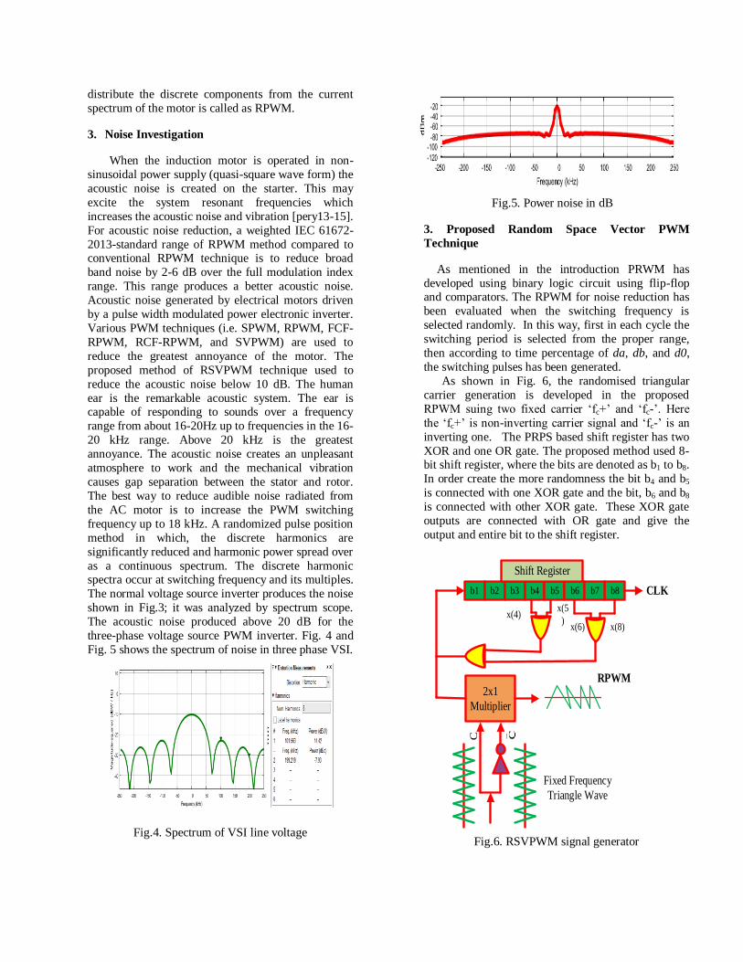
The normal voltage source inverter produces the noise
shown in Fig.3; it was analyzed by spectrum scope.
The acoustic noise produced above 20 dB for the
three-phase voltage source PWM inverter. Fig. 4 and
Fig. 5 shows the spectrum of noise in three phase VSI.
Fig.4. Spectrum of VSI line voltage
Fig.5. Power noise in dB
3. Proposed Random Space Vector PWM
Technique
As mentioned in the introduction PRWM has
developed using binary logic circuit using flip-flop and comparators. The RPWM for noise reduction has
been evaluated when the switching frequency is
selected randomly. In this way, first in each cycle the
switching period is selected from the proper range,
then according to time percentage of da, db, and d0,
the switching pulses has been generated.
As shown in Fig. 6, the randomised triangular
carrier generation is developed in the proposed
RPWM suing two fixed carrier „fc+‟ and „fc-‟. Here
the „fc+‟ is non-inverting carrier signal and „fc-‟ is an
inverting one. The PRPS based shift register has two
XOR and one OR gate. The proposed method used 8-bit shift register, where the bits are denoted as b1 to b8.
In order create the more randomness the bit b4 and b5
is connected with one XOR gate and the bit, b6 and b8
is connected with other XOR gate. These XOR gate
outputs are connected with OR gate and give the
output and entire bit to the shift register.
Fixed Frequency
Triangle Wave
2x1
Multiplier
C
b1 b2 b3 b4 b5 b6 b8b7
x(4)x(5
)x(6) x(8)
Shift Register
RPWM
CLK
Fig.6. RSVPWM signal generator

VUV
VVW
VWU
t in sec
All of the register elements share a common clock input,
which is omitted from the symbol for reasons of clarity. The
data input to the LFSR is generated by XOR or XNOR the
tap bits; the remaining bits function as a standard shift
register. The sequence of values generated by an LFSR is
determined by its feedback function (XOR against XNOR)
and tap selection. For example, consider two 2-bit XOR
based LFSRs with different tap selections (Fig.6). Based on
the OR-gate output the multiplier receiving signal from either
from „fc+‟ or „fc-. The correspondence switching states
selection is chosen based on the pulse pattern output.
4. Simulation and Results
The proposed RPWM is modeled with six switch voltage source inverter with 0.75kW induction motor using
MATLAB/Simulink platform. The table2 illustrates the
parameters of simulation for inverter and induction motor.
Table 2. Simulation parameters
The highest randomization freedoms, nonlinearities
components, dead-time and filters have been ignored in the
simulation. The simulation study is developed for the PWM
switching frequency in tuned with 1 kHz to 25 kHz frequency
range. The VSI line voltage (VL) with high modulation index, Ma= 0.9. Now, when the VSI functioned at 0.9 Ma, the voltage
is measured as 270V. Fig.8 illustrates the THD spectrum for
line –voltage, where the percentage line-voltage THD is
observed as 10.16% for Ma= 0.9 .
Fig. 7 RSVPWM VSI line voltage, Ma=0.9.
Fig. 8 Harmonics spectrum of line voltage, Ma=0.9
(a)
Parameters values
Power (P) 1 KW
Line to Line voltage (VL) 400 V
Frequency (f) 50 Hz
Stator resistance (Rs) 1.4 Ω
Stator inductance (Ls) 0.00587 H
Rotor resistance (Rr) 1.35 Ω
Speed 1400 rpm
Irms 3 A
Vrms 400V
Torque(T) 5Nm
(b)
(c)
Fig. 9. Simulation results of the motor voltage
spectrum for modulation index 0.5, 0.7 and 0.9 for
4kHz.
(a)
(b)
(c)
Fig. 10. Simulation results of the motor voltage
spectrum for modulation index 0.5, 0.7 and 0.9 for
4kHz.
The Fig.9 and Fig.10 shows the voltage spectrum for VSI functioned at lower for modulation index 0.5,
0.7 and 0.9 for 4kHz. Here, when the inverter
operating
Ma = 0.5, the noise is measured as 22.14 dB.
However, the, when inverter operating at Ma = 0.9, for
the same switching frequency range, voltage noise is
measured as 16.29 dB. From the results, when lower
modulation ranges the voltage waveform had higher
noise against higher Ma.
5. Experimental Results
For the investigation of the experimental
verification for the proposed RPWM, the 200W show
six switch VSI is designed and collaborated with PIC
microcontroller digital implementation platform.
Fig.11.shows the experimental setup of the three-phase
VSI connected RL load

The RPWM is developed in assembly code and
implemented in the 5 kHz switching frequency with 5
mircosec dead time. Fig.11.shows the experimental
setup of the three-phase VSI connected RL load. The
1000mcroF capacitor and 10 ohm, 4 mH RL load used
for the DC-link and load respectably. The TLP250 gate driver circuit is used for six MOSFETs. The voltage and
THD waveforms are measured using 2 channel DSO.
The inverter is having a degree of freedom to change
their modulation index.
The Fig.12 shows the gating pulses of inverter switch
T1 to T2 , Fig.13 shows the gating pulses of inverter
switch T3 to T4, and Fig.14 shows the gating pulses of
inverter switch T5 to T6. The dead time of the same
inverter leg switch is shown in fig.15. At first the test
was performed between 5kHz lower modulation index
(Ma= 0.5) and the inverter tested for higher modulation
index (Ma=0.9). The output line voltage of VSI for 4kHz is shown in Fig.16. Here, the line voltage of the
inverter is measured as 60V. In this case the noise is
calculated as 9.8 dB and it is rising slightly when the
switching frequency rising to 11 dB for 6kHz, fs. In
similar way, when inverter is operates at higher Ma 0.9,
the output line voltage of VSI for 4kHz is shown in
Fig.17. Here, the line voltage of the inverter is
measured as 120V. In this case the noise is calculated
as 14.8 dB and it is rising slightly when the switching
frequency rising to 9 dB for 4kHz. The fig.44 shows the
line voltage THD spectra for Ma=0.9. From the results, the THD is measured as lesser values as
sec
S1,
S2
S1, S2
Fig.12. gating pulses of inverter switch S1 to S2
sec
S3,
S4
S3 S4
Fig.13. gating pulses of inverter switch S3 to S4
sec
S5,
S6
S6 S5
Fig.14. gating pulses of inverter switch S5 to S6
sec
S5,
S6
S5
S6
Fig.15. gating pulses of inverter switch S2 to S3
sec
Vin
Fig.16. Experimental Line voltage for 0.5 Ma
sec
Vin
Fig.17. Experimental Line voltage for 0.9 Ma
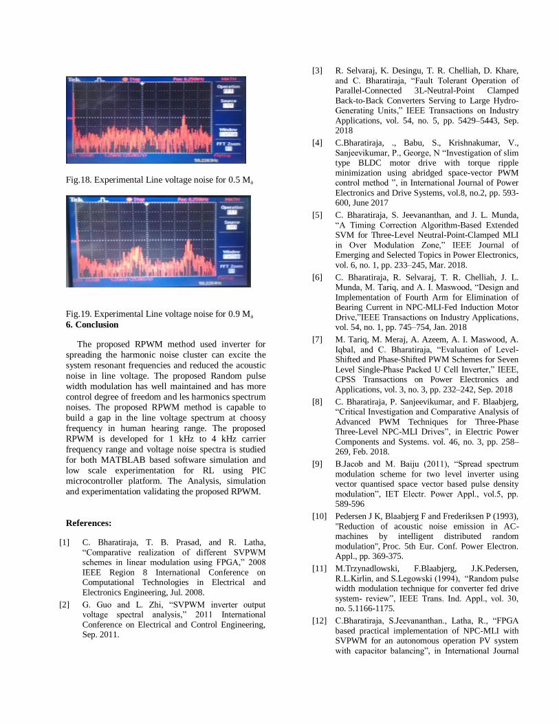
Fig.18. Experimental Line voltage noise for 0.5 Ma
Fig.19. Experimental Line voltage noise for 0.9 Ma
6. Conclusion
The proposed RPWM method used inverter for
spreading the harmonic noise cluster can excite the
system resonant frequencies and reduced the acoustic
noise in line voltage. The proposed Random pulse
width modulation has well maintained and has more
control degree of freedom and les harmonics spectrum noises. The proposed RPWM method is capable to
build a gap in the line voltage spectrum at choosy
frequency in human hearing range. The proposed
RPWM is developed for 1 kHz to 4 kHz carrier
frequency range and voltage noise spectra is studied
for both MATBLAB based software simulation and
low scale experimentation for RL using PIC
microcontroller platform. The Analysis, simulation
and experimentation validating the proposed RPWM.
References:
[1] C. Bharatiraja, T. B. Prasad, and R. Latha,
“Comparative realization of different SVPWM schemes in linear modulation using FPGA,” 2008
IEEE Region 8 International Conference on Computational Technologies in Electrical and
Electronics Engineering, Jul. 2008.
[2] G. Guo and L. Zhi, “SVPWM inverter output voltage spectral analysis,” 2011 International
Conference on Electrical and Control Engineering, Sep. 2011.
[3] R. Selvaraj, K. Desingu, T. R. Chelliah, D. Khare,
and C. Bharatiraja, “Fault Tolerant Operation of Parallel-Connected 3L-Neutral-Point Clamped
Back-to-Back Converters Serving to Large Hydro-Generating Units,” IEEE Transactions on Industry
Applications, vol. 54, no. 5, pp. 5429–5443, Sep. 2018
[4] C.Bharatiraja, ., Babu, S., Krishnakumar, V.,
Sanjeevikumar, P., George, N “Investigation of slim type BLDC motor drive with torque ripple
minimization using abridged space-vector PWM control method ”, in International Journal of Power
Electronics and Drive Systems, vol.8, no.2, pp. 593-600, June 2017
[5] C. Bharatiraja, S. Jeevananthan, and J. L. Munda,
“A Timing Correction Algorithm-Based Extended SVM for Three-Level Neutral-Point-Clamped MLI
in Over Modulation Zone,” IEEE Journal of Emerging and Selected Topics in Power Electronics,
vol. 6, no. 1, pp. 233–245, Mar. 2018.
[6] C. Bharatiraja, R. Selvaraj, T. R. Chelliah, J. L. Munda, M. Tariq, and A. I. Maswood, “Design and
Implementation of Fourth Arm for Elimination of Bearing Current in NPC-MLI-Fed Induction Motor
Drive,”IEEE Transactions on Industry Applications, vol. 54, no. 1, pp. 745–754, Jan. 2018
[7] M. Tariq, M. Meraj, A. Azeem, A. I. Maswood, A.
Iqbal, and C. Bharatiraja, “Evaluation of Level-Shifted and Phase-Shifted PWM Schemes for Seven
Level Single-Phase Packed U Cell Inverter,” IEEE, CPSS Transactions on Power Electronics and
Applications, vol. 3, no. 3, pp. 232–242, Sep. 2018
[8] C. Bharatiraja, P. Sanjeevikumar, and F. Blaabjerg, “Critical Investigation and Comparative Analysis of
Advanced PWM Techniques for Three-Phase Three-Level NPC-MLI Drives”, in Electric Power
Components and Systems. vol. 46, no. 3, pp. 258–269, Feb. 2018.
[9] B.Jacob and M. Baiju (2011), “Spread spectrum
modulation scheme for two level inverter using vector quantised space vector based pulse density
modulation”, IET Electr. Power Appl., vol.5, pp. 589-596
[10] Pedersen J K, Blaabjerg F and Frederiksen P (1993),
"Reduction of acoustic noise emission in AC-machines by intelligent distributed random
modulation", Proc. 5th Eur. Conf. Power Electron. Appl., pp. 369-375.
[11] M.Trzynadlowski, F.Blaabjerg, J.K.Pedersen,
R.L.Kirlin, and S.Legowski (1994), “Random pulse width modulation technique for converter fed drive
system- review”, IEEE Trans. Ind. Appl., vol. 30, no. 5.1166-1175.
[12] C.Bharatiraja, S.Jeevananthan., Latha, R., “FPGA
based practical implementation of NPC-MLI with SVPWM for an autonomous operation PV system
with capacitor balancing”, in International Journal

of Electrical Power and Energy Systems/ Elsevier,
vol. 61, pp.489-509, Oct 2014
[13] Peyghambari A, Dastfan A and Ahmadyfard A
(2015), "Strategy for switching period selection in random pulse width modulation to shape the noise
spectrum", IET Power Electron., vol. 8, pp. 517-
523.
[14] Pedersen J K, Blaabjerg F and Frederiksen P (1993),
"Reduction of acoustic noise emission in AC-machines by intelligent distributed random
modulation", Proc. 5th Eur. Conf. Power Electron.
Appl., pp. 369-375.
[15] Blaabjerg F, Pedersen J.K, Ritchie E and Nielsen P
(1995), "Determination of mechanical resonances in induction motors by random modulation and
acoustic measurement", IEEE Trans. Ind. Appl., vol.
31, no. 4, pp. 823-829.
[16] Jiang D and Wang F (2013), "Variable switching
frequency PWM for three-phase converters based on current ripple prediction", IEEE Trans. Power
Electron., vol. 28, no. 11, pp. 4951-4961.
[17] Mathe G, Lungeanu F, Sera D, Rasmussen P. O. and Pedersen J. K. (2012), "Spread spectrum
modulation by using asymmetric-carrier random PWM", IEEE Trans. Ind. Electron., vol. 59, no. 10,
pp. 3710-3718.
[18] Bech M.M, Blaabjerg. F and Pedersen J. K. (2000), "Random modulation techniques with fixed
switching frequency for three-phase power converters", IEEE Trans. Power Electron., vol. 15,
no. 4, pp. 753-761.
[19] Trzynadlowski A. M, Borisov K, Li Y, Qin L and Wang Z (2004), "Mitigation of electromagnetic
interference and acoustic noise in vehicular drives by random pulse width modulation", Proc. Power
Electron. Transp., pp. 67-71
[20] C. Bharatiraja, T. B. Prasad, and R. Latha, “Comparative realization of different SVPWM
schemes in linear modulation using FPGA,” 2008 IEEE Region 8 International Conference on
Computational Technologies in Electrical and
Electronics Engineering, Jul. 2008M
[21] Pedersen J K, Blaabjerg F and Frederiksen P (1993),
"Reduction of acoustic noise emission in AC-machines by intelligent distributed random
modulation", Proc. 5th Eur. Conf. Power Electron.
Appl., pp. 369-375.
[22] Blaabjerg F, Pedersen J.K, Ritchie E and Nielsen P
(1995), "Determination of mechanical resonances in induction motors by random modulation and
acoustic measurement", IEEE Trans. Ind. Appl., vol.
31, no. 4, pp. 823-829.
[23] C.Bharatiraja, S. Jeevananthan, S, R. Latha, and
V.Mohan, “Vector selection approach-based hexagonal hysteresis space vector current controller
for a three phase diode clamped MLI with capacitor
voltage balancing ,” IET Power Electronics., vol. 9,
no. 7, pp. 1350-1361, June 2016.
[24] Santhakumar, C., Shivakumar, R., Bharatiraja, C.,
Sanjeevikumar, P. “Carrier shifting algorithms for the mitigation of circulating current in diode
clamped MLI fed induction motor drive ”, in
International Journal of Power Electronics and Drive Systems, vol.8, no.2, pp. 844-852, June 2017
[25] C. Bharatiraja, S. Jeevananthan, J.L. Munda, and R. Latha, “Improved SVPWM vector selection
approaches in OVM region to reduce common-
mode voltage for three-level neutral point clamped inverter,” International Journal of Electrical Power
& Energy Systems/ Elsevier, vol. 79, no. 1, pp. 285–297, Oct. 2016.
[26] C.Bharatiraja,R.Latha, S.SDash, R.Gulati, R, and
P.V Sharma, “A 3D-SVPWM algorithm design and its FPGA IP-core implementation for MLIS
operating over a wide modulation range”,International Review of Electrical
Engineering, vol.8 ,no. 3 pp. 947-961,2013\
[27] Mathe G, Lungeanu F, Sera D, Rasmussen P. O. and Pedersen J. K. (2012), "Spread spectrum
modulation by using asymmetric-carrier random PWM", IEEE Trans. Ind. Electron., vol. 59, no. 10,
pp. 3710-3718.
[28] A. Ruiz-Gonzalez, F. Vargas-Merino, J. R. Heredia-Larrubia, M. J. MecoGutierrez, and F. Perez-
Hidalgo, “Application of slope PWM strategies to reduce acoustic noise radiated by inverter-fed
induction motors,” IEEE Trans. Ind. Electron., vol. 60, no. 7, pp. 2555–2563, Jul. 2013.
[29] T. Pu, F. Bu, W. Huang, and L. Zhu,
“Implementation of random SVPWM strategy for three-phase voltage source inverter based on
FPGA,” 2017 20th International Conference on Electrical Machines and Systems (ICEMS), Aug.
2017.
[30] K. Lee, G. Shen, W. Yao, and Z. Lu, “Performance Characterization of Random Pulse Width
Modulation Algorithms in Industrial and Commercial Adjustable-Speed Drives,” IEEE
Transactions on Industry Applications, vol. 53, no. 2, pp. 1078–1087, Mar. 2017.
[31] P. Anbarasan,S. Ramkumar and C.Bharatiraja,“A
Comprehensive Analysis of Carrier Shifting Algorithms for Diode-Clamped MLI Based Drive”,
in Journal of Electrical Engineering, Vol.17, No.2, 2017, pp.52- 61, 2017.
[32] C.Bharatiraja, R.Latha, S.Jeevananthan, S.Raghu
and S.S. Dash, "Design And Validation Of Simple Space Vector PWM Scheme For Three-Level
NPC– MLI With Investigation Of DC Link Imbalance Using FPGA -IP Core ", Journal of
Electrical Engineering , vol.13, no. 1, pp 54-63, March 2013.