the past, present, and future of silicon...
TRANSCRIPT

The Past, Present, and Future ofSilicon Photonics
Myung-Jae LeeHigh-Speed Circuits & Systems Lab.
Dept. of Electrical and Electronic EngineeringYonsei University
Outline
Introduction
A glance at history
Present achievements (2006)
Future Prospects
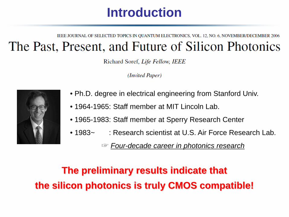
Introduction
• Ph.D. degree in electrical engineering from Stanford Univ.
• 1964-1965: Staff member at MIT Lincoln Lab.
• 1965-1983: Staff member at Sperry Research Center
• 1983~ : Research scientist at U.S. Air Force Research Lab.
☞ Four-decade career in photonics research
The preliminary results indicate thatthe silicon photonics is truly CMOS compatible!
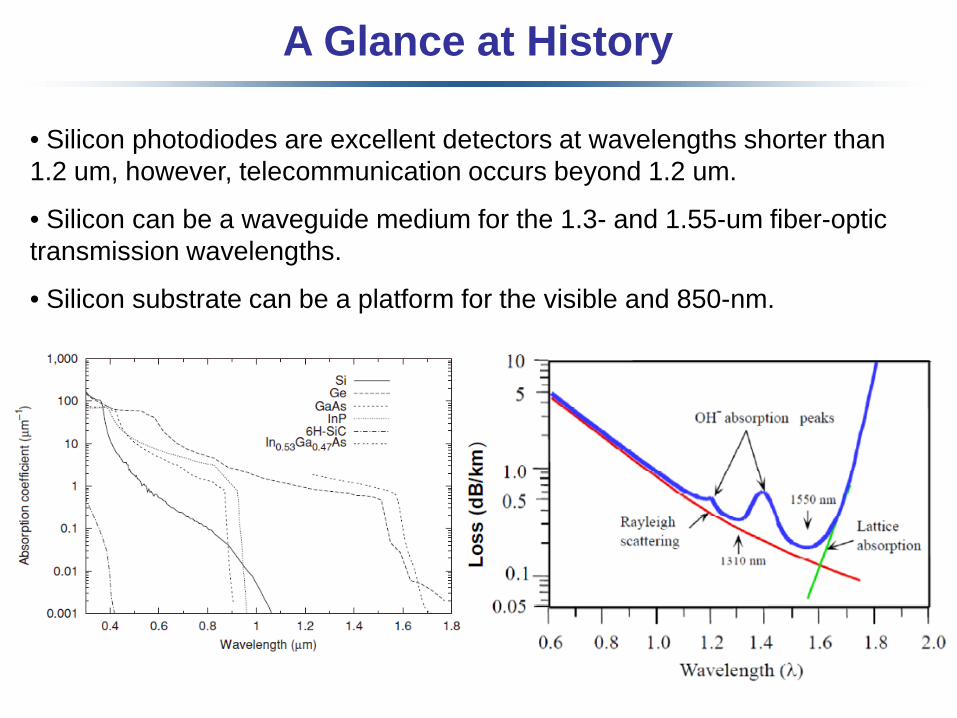
A Glance at History
• Silicon photodiodes are excellent detectors at wavelengths shorter than 1.2 um, however, telecommunication occurs beyond 1.2 um.
• Silicon can be a waveguide medium for the 1.3- and 1.55-um fiber-optic transmission wavelengths.
• Silicon substrate can be a platform for the visible and 850-nm.
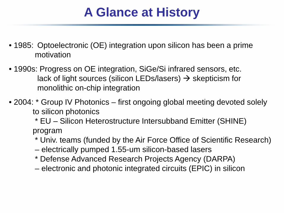
A Glance at History
• 1985: Optoelectronic (OE) integration upon silicon has been a primemotivation
• 1990s: Progress on OE integration, SiGe/Si infrared sensors, etc.lack of light sources (silicon LEDs/lasers) skepticism for monolithic on-chip integration
• 2004: * Group IV Photonics – first ongoing global meeting devoted solelyto silicon photonics* EU – Silicon Heterostructure Intersubband Emitter (SHINE) program* Univ. teams (funded by the Air Force Office of Scientific Research) – electrically pumped 1.55-um silicon-based lasers* Defense Advanced Research Projects Agency (DARPA)– electronic and photonic integrated circuits (EPIC) in silicon

Present Achievements (2006)
• Development of high-volume optoelectronic integrated circuit (OEIC) chips and practical photonic ICs
• Optical interconnects: rack-to-rack, board-to-board, chip-to-chip, intra-chip
• Potential uses of silicon photonics
- photonic interconnects, data communication, telecommunication, signal processing, switched networks, imaging, display, radio frequency/wireless photonics, electronic warfare, photonics for millimeter-wave/microwave/radio-frequency systems, bionics, optical storage, etc.
Recent explosion in Si photonics
Present AchievementsA. Electronic and Photonic Integration
B. Silicon Raman Lasers
C. Erbium-Silicon Lasers
D. Ultrafast Group IV Electrooptical Modulators
E. Direct-Bandgap SiGeSn/Ge/GeSn Heterostructure/QW Devices
F. Electrically Pumped Group IV Laser for 1.2-1.6 um
G. Hybrid Integration of III-V Lasers on Si
H. Active Microresonator Devices
I. PhC Devices
J. Plasmon Optics
K. The Long-Wave Infrared (LWIR) Paradigm for Silicon Integrated Photonics
L. Nonlinear Optical (NLO) Devices
A) Electronic and Photonic Integration
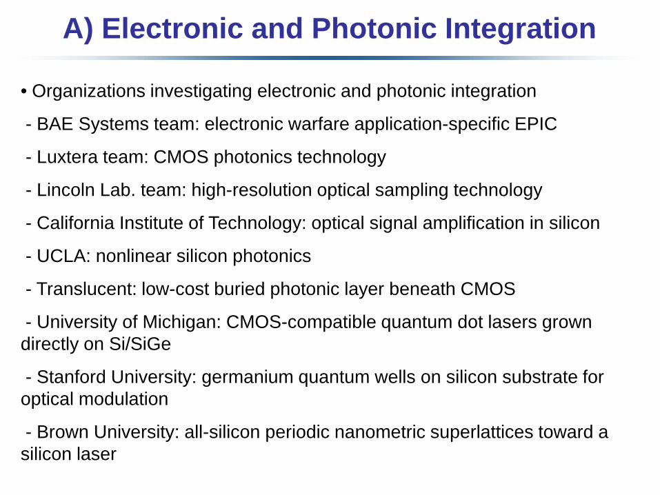
• Organizations investigating electronic and photonic integration
- BAE Systems team: electronic warfare application-specific EPIC
- Luxtera team: CMOS photonics technology
- Lincoln Lab. team: high-resolution optical sampling technology
- California Institute of Technology: optical signal amplification in silicon
- UCLA: nonlinear silicon photonics
- Translucent: low-cost buried photonic layer beneath CMOS
- University of Michigan: CMOS-compatible quantum dot lasers grown directly on Si/SiGe
- Stanford University: germanium quantum wells on silicon substrate for optical modulation
- Brown University: all-silicon periodic nanometric superlattices toward a silicon laser
A) Electronic and Photonic Integration
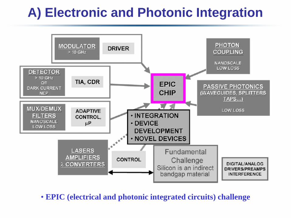
• EPIC (electrical and photonic integrated circuits) challenge
A) Electronic and Photonic Integration
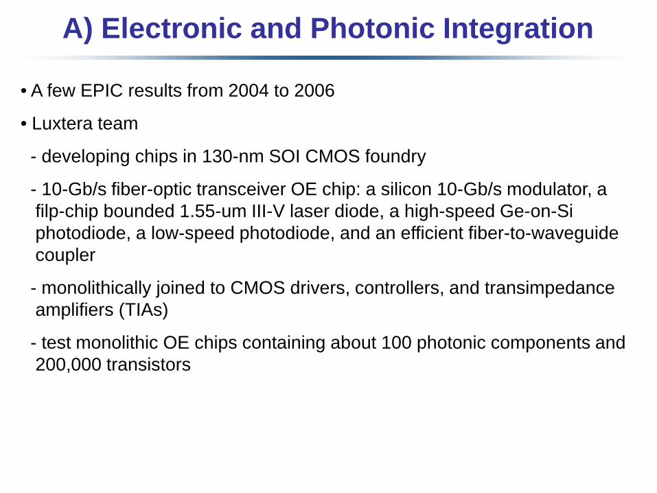
• A few EPIC results from 2004 to 2006
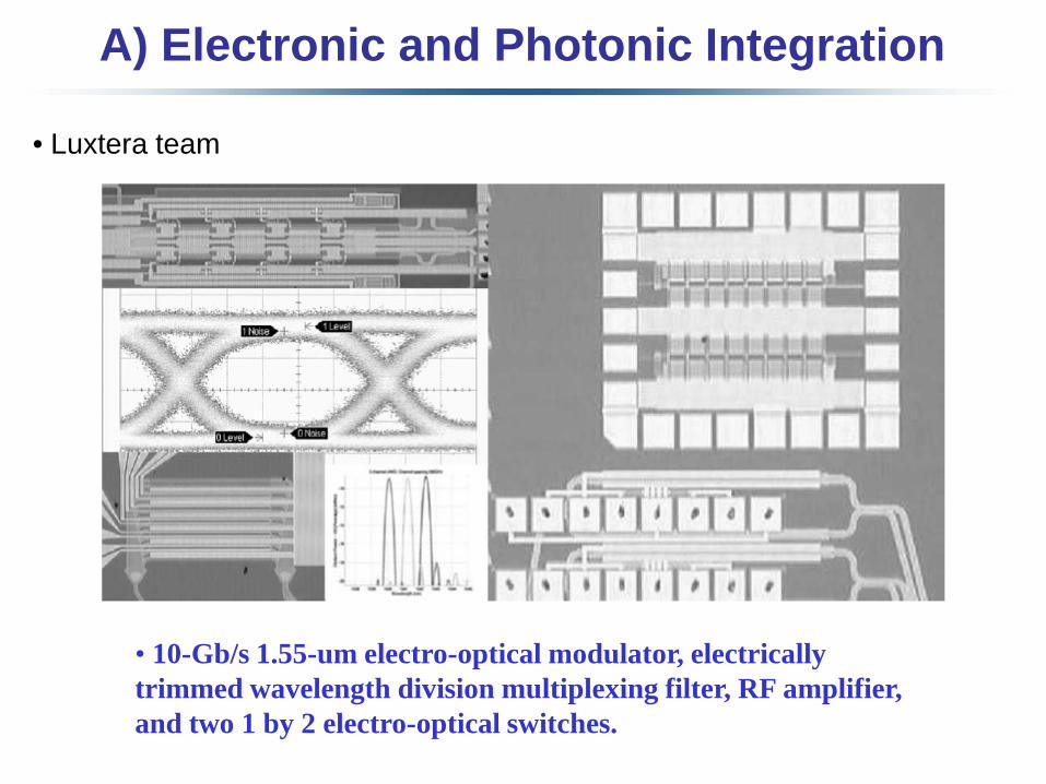
• Luxtera team
- developing chips in 130-nm SOI CMOS foundry
- 10-Gb/s fiber-optic transceiver OE chip: a silicon 10-Gb/s modulator, a filp-chip bounded 1.55-um III-V laser diode, a high-speed Ge-on-Si photodiode, a low-speed photodiode, and an efficient fiber-to-waveguide coupler
- monolithically joined to CMOS drivers, controllers, and transimpedance amplifiers (TIAs)
- test monolithic OE chips containing about 100 photonic components and 200,000 transistors
A) Electronic and Photonic Integration
• Luxtera team
• 10-Gb/s 1.55-um electro-optical modulator, electrically trimmed wavelength division multiplexing filter, RF amplifier, and two 1 by 2 electro-optical switches.

A) Electronic and Photonic Integration
• Luxtera team
• Microscope photographs of SOI integrated-photonic test network including microring filter and fiber-to-waveguide coupler
• 1.55-um optical coupling between single-mode fiber and SOI strip waveguide
B/C) Silicon Raman/Erbium-Silicon Lasers
• Development of the silicon Raman lasers
- UCLA, Intel Corporation
- fully integrateable
- low gain
- performance improvements needed
- needed for optical pumping (it takes a laser to make a laser)
• Development of the Erbium-Silicon lasers
- Electrically pumped lasers
- more desirable in OE chips

D) Ultrafast Group IV Electrooptical Modulators
• Using Group IV materials: carbon, silicon, stannum, etc.
- optically driven SOI plasma-effect modulator; 20-ps rates
- carrier-injected split-ridge waveguide modulator in double SOI; 24 GHz
- silicon Mach–Zehnder modulator; 6-10-Gb/s data transmission
- a sub-micron depletion-type photonic modulator in SOI; 3-7-ps rates
- SOI-waveguided modulator; 10 Gb/s
- germanium quantum-well modulator on silicon
- electroabsorption modulator (EAM)
E) Direct-Bandgap SiGeSn/Ge/GeSnHeterostructure/QW Devices
• for direct band-to-band photonic devices
• many possibilities for direct-gap conduction-to-valence photonic devices- laser diodes, LEDs, photodetectors, and modulators
• operating in the near- and midinfrared regions
- SnGe on Si for strain-balanced Ge/SnGe quantum well heterostructures
- Si–Ge–Sn semiconductors on Si(100) via Sn
- Si-based Ge/GeSn multiple quantum wells (MQWs)
• Critical challenge for this technology: compatible with a CMOS foundry?
F) Electrically Pumped Group IV Laser for 1.2-1.6 umG) Hybrid Integration of III-V Lasers on Si
• IV-IV lasers
- Electrically pumped Group IV semiconductor micro-ring laser
- Stimulated emission in a nanostructured silicon pn junction diode using current injection
- Stimulated emission in periodic nanopatterned silicon
• III-V lasers: integrating of III-V laser diodes on silicon
- Electrically pumped hybrid AlGaInAs-silicon evanescent laser
- CMOS-compatible quantum-dot lasers grown directly on Si/SiGe
Most manufacturable method / lowest cost per performance
H) Active Microresonator Devices
• Miniaturization: to reduce the “footprint” of silicon photonic components
larger scale of on-chip integration
• Resonators can form the basis of a laser, a light emitter, a photodetector, a modulator, or a spatial routing switch.
- active microring modulator
- 10-Gb/s intensity modulator in an SOI microring
- silicon microring optical routing switches
- electro-optical and optical–optical switching of dual microring resonator waveguide systems
- dual-microring-resonator cross-connect switches and modulators
I) PhC Devices
• Photonic crystal (PhC) can yield devices with unique properties
- negative-refraction lenses, superprisms, sharp waveguide bends, all-optical buffer memories, dynamic dispersion compensators, nanoscale 3-D point-defect resonators, etc.
• Active devices are feasible using PhC.
- silicon-based PhC laser diode
- silicon PhC line-defect waveguides
- SOI PhC line-defect waveguides
PhC devices can be made in a CMOS facility.
PhC devices can be a part of the high-performance OEIC in future
J) Plasmon Optics
• Plasmon optics can open a new domain for integrated photonics based on:
1) compact, low-power optical devices
2) optical imaging systems with nanometer-scale resolution
3) enhanced light emission from active photonic devices via coupling to surface plasmons
4) coupling from dielectric (fiber and SOI waveguide) photonics to plasmonic devices
K) The Long-Wave Infrared (LWIR) Paradigmfor Silicon Integrated Photonics
• Opportunities for sensing, communications, signal processing, missile detection, tracking, and imaging in the “wide infrared,” expecially in the 3-5 and 8-14 um windows, in a band near 20 um, and in the 30-100-um “terahertz” range.
• Si-based OEICs can operate at a wavelength anywhere from 1.2 to 100 um.
- Silicon waveguides with low propagation loss for wide infrared:* silicon rib-membrane for 1.2-6.0 and 24-100 um* germanium rib on silicon for 1.9-14 um* Si-based air-filled hollow-core channel waveguide for 1.2-100 um
- long-wave Si-based photodetectors, modulators, and light emitter
L) Nonlinear Optical (NLO) Devices
• Nonlinear optical effects in silicon are relatively strong.
- Franz-Keldysh shift
- Kerr effect
- stimulated Raman scattering
- coherent anti-Stokes Raman scattering
- two-photon absorption
- intensity-dependent refractive index
- four-wave mixing
Future Prospects
1) True OE integration on CMOS in a stable 130-nm or 90-nm commercial process
2) Hundreds of photonic components and more than a million transistors on a monolithic OE chip
3) Cost-effective fiber-optic links using Si OE transceivers at 10-100 Gb/s
4) Fast, cost-effective optical interconnection of computer chips
5) Integrated Ge-on-Si photodiodes as the 1.55 um detectors-of-choice in PICs and OEICs
6) A room-temperature electrically pumped Ge/Si laser
7) A well-developed Ge/GeSn technology-both MQWs and heterodiodes-that includes 1.55-um band-to-band laser diodes, LEDs, modulators, and photodetectors

Future Prospects
8) Silicon laser diodes that rely upon Erbium ions
9) Integration of silicon PhC devices into high-performance silicon photonic circuits
10) Development of practical Si-based Group IV components for the wide infrared spectrum stretching beyond 1.6 um out to 100 um-components
11) Ultrasmall, nanophotonic Ge-in-Si p-i-n lasers, modulators, and detectors
12) Si-based photonic devices utilizing Group IV quantum dots or QWs