the nasa electronic parts and packaging (nepp) … · web viewnasa electronic parts and packaging...
TRANSCRIPT
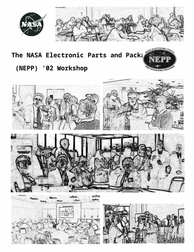
The NASA Electronic Parts and Packaging (NEPP) ‘02 Workshop
1

The
NASA Electronic Parts and Packaging
(NEPP) ‘02 Workshop
April 30 - May 2, 2002
Hilton
Nassau Bay & Marina
Houston, TX
Organized by:
NEPP Information, Management and Dissemination Project
2
Message ________________________ from Chuck Barnes, NEPP Program Manager
Welcome to the Annual NEPP Workshop on Electronic Parts, Packaging, and Radiation Characterization for Space Applications! We’re happy you are with us and look forward to talking with you. Let’s start off with a few words about the NASA Electronic Parts and Packaging (NEPP) Program. The NEPP objectives are to:
Assess the reliability of newly available electronic parts and packaging technologies for usage on NASA projects through validations, assessments and characterizations and the development of test methods/tools.
Expedite infusion paths for advanced (emerging) electronic parts and packaging technologies by evaluations of readiness for manufacturability and project usage considerations.
Provide NASA Projects with technology selection, application, and validation guidelines for electronic parts and packaging hardware and processes.
Retain and disseminate electronic parts and packaging assurance, reliability validations, tools and availability information to the NASA community.
NEPP is organized around three technology concentrations and the Information Management and Dissemination effort. The technology concentrations are Electronic Parts (EPAR), Electronic Packaging (EPAC), and Electronic Radiation Characterization (ERC). The Information Management & Dissemination (IMD) project is responsible for making all NEPP products and deliverables accessible in a controlled manner and is coordinating this conference.
The Electronic Parts Project is tied to satisfying the needs of NASA programs/projects for evaluation of newly available and advanced electronic parts and maximizing effectiveness and efficiency through leveraging by teaming and partnering with industry and other agencies. The objective of the NEPP Electronic Packaging Project is to stay ahead of Mission project requirements by 18-24 months. The primary goal of the Project is to expedite cutting-edge technology into missions and instruments during the Mission Formulation phases, to obtain electronics packaging information, and to sustain the availability of that information for broad usage across the Agency, industry, academia, and other government agencies. The Electronics Radiation Characterization Project of NEPP characterizes the effects of radiation on electronics. Long and short term radiation effects such as total ionizing dose (TID), displacement damage (DD), and single event effects (SEE) provide aerospace designers’ a myriad of challenges for system design. The ERC Project is responsible for supporting NASA’s current and future needs for electronic systems in the natural space and terrestrial radiation environments.
3
Keynote Speaker_______________
Biographical Data
Lyndon B. Johnson Space CenterHouston, Texas 77058
National Aeronautics and Space Administration
NAME: John D. Olivas (PhD.)NASA Astronaut (Mission Specialist Candidate)
PERSONAL DATA: Born in North Hollywood, California, but considers El Paso, Texas to be his hometown. Married and has 4 children. Recreational interests include running weightlifting hunting, fishing, surfing, and mountain biking.
EDUCATION: Graduate of Burges High School, El Paso, Texas; received a bachelor of science degree in mechanical engineering from the University of Texas-El Paso; a masters of science degree in mechanical engineering from the University of Houston and a doctorate in mechanical engineering and materials science from Rice University.
ORGANIZATIONS: American Society of Materials International (ASM International), Texas Registered Professional Engineer.
AWARDS: Four U.S. Patents; Four NASA Class One Tech Brief Awards; Five JPL-California Institute of Technology Novel Technology Report Recognitions; HENAAC Most Promising Engineer, McDonald's Hispanos Triunfadores Award, NASA ASEE Summer Faculty Fellowship Award, Dow Life Saving Award.
EXPERIENCE: After graduating with his undergraduate degree, Olivas worked for the Dow Chemical Company in Freeport, Texas. While there, he was a mechanical/materials engineer responsible for performing equipment stress/failure analysis for the operating facilities. After completing his master's degree, Olivas left to pursue his doctorate while supporting engine-coating evaluations for C-5 maintenance operations at Kelly Air Force Base. He also supported the Crew and Thermal Systems Directorate at NASA Johnson Space Center, evaluating materials for application to the next generation Extravehicular Mobility Unit, during a summer intern.
Upon completing his doctorate, he was offered a senior research engineer position at the Jet Propulsion Laboratory (JPL). His research included the development of tools and methodologies for nondestructively evaluating microelectronics and structural materials subjected to space environments. He was promoted to Program Manager of the JPL Advanced Interconnect and Manufacturing Assurance Program aimed at evaluating die reliability and susceptibility of state-of-the-art microelectronics for use in future NASA projects. Through his career, he has authored and presented numerous papers at technical conferences and in scientific journals and is principal developer of seven inventions.
NASA EXPERIENCE: NASA selected Olivas for assignment as Astronaut in 1998. Astronaut Training includes orientation briefings and tours, numerous scientific and technical briefings, intensive instruction in Shuttle and International Space Station system, physiological training and ground school to prepare for T-38 flight training, as well as learning water and wilderness survival techniques. He is currently assigned technical responsibilities within the Robotics Branch of the Astronaut Office. He serves as lead for the Special Purpose Dexterous Manipulator Robot, Mobile Transporter and the Mobile Base. System.
JUNE 2001
4

Program___________________________
Tuesday, 30 April8:00am Welcome – Phil Zulueta, JPL
8:05 The NEPP Program – Chuck Barnes, NEPP Program Manager, JPL
8:15 Keynote Presentation – John D. Olivas, Ph.D, NASA Astronaut (Mission Specialist Candidate)
Session 1 – High Temperature Environments Session Chairs: Liangyu Chen, GRC
8:45 “New and Emerging Packaging Technologies for Harsh Environments”, Robert S. Okojie, GRC and Ender Savrun, Sienna Technologies et al
9:10 “High Temperature Reliability of PEMs Using New Molding Compounds”, F.P. McCluskey, A. Chandrasekaran and C. O'Connor, University of Maryland et al
9:35 “Structure Optimization of Wire-bond for High Temperature Operation”, Shun-Tien Lin, UTRC and Xiaodong Luo et al
10:00 Break
Session 2 – Low Temperature Environments I Session Chair: Mike Newell, JPL
10:20 “Ceramic Temperature Operation over Extreme Temperatures”, Elaine Gee, Muses-CN Nanorover Project, JPL
10:45 “SOI Device Optimization for Low Temperature and Radiation Tolerance”, Jagdish Patel, JPL, John Cressler, Ying Li, Auburn University
11:10 “Hot Carrier Degradation Effects in Power MOSFETs Operating at Cryogenic Temperatures”, Elaine Gee and Michael Newell, JPL
11:35 “Chip On Board, a path to Extreme Temperature Operation of Space Electronics”, Ken Hicks, JPL
12:00 Lunch
Session 3 - LaRC-MFC Technology Session Chair: James Bockman, LaRC
1:30 “Overview of NASA-Langley Macro-Fiber Composite (MFC) Piezoelectric Actuator Technology”, W. Keats Wilkie, Army Research Laboratory; LaRC
1:55 “Design and Characterization of Radial Field Diaphragms”, Robert G. Bryant, NASA Langley Research Center
2:20 “Reliability Testing of MFC Actuators”, James W. High et al, LaRC
2:45 “Miniaturizing High Voltage Amplifiers for Piezoelectric Actuators”, Paul Robinson and James Bockman, LaRC
3:10 Break
Session 4 – Innovative Qualification and Test Methods Session Chair: Phil Zulueta, JPL
3:25 “Fiber Optic Cable Assembly Characterization Studies at Goddard Space Flight Center”, Melanie Ott, GSFC
3:50 “Rapid Qualification of Area Array Package Assemblies by Increase of Ramp Rates and Temperature Ranges”, Reza Ghaffarian, JPL
4:15 “Qualification of SoC for Spacecraft Avionics Applications”, Jonathan Perret, JPL
4:40 “Characterization of Integrated Fiber Optical Modulators for Space Flight”, Melanie Ott, GSFC
5:05 MSU Activity…Ken LaBel, GSFC
5

Program___________________________
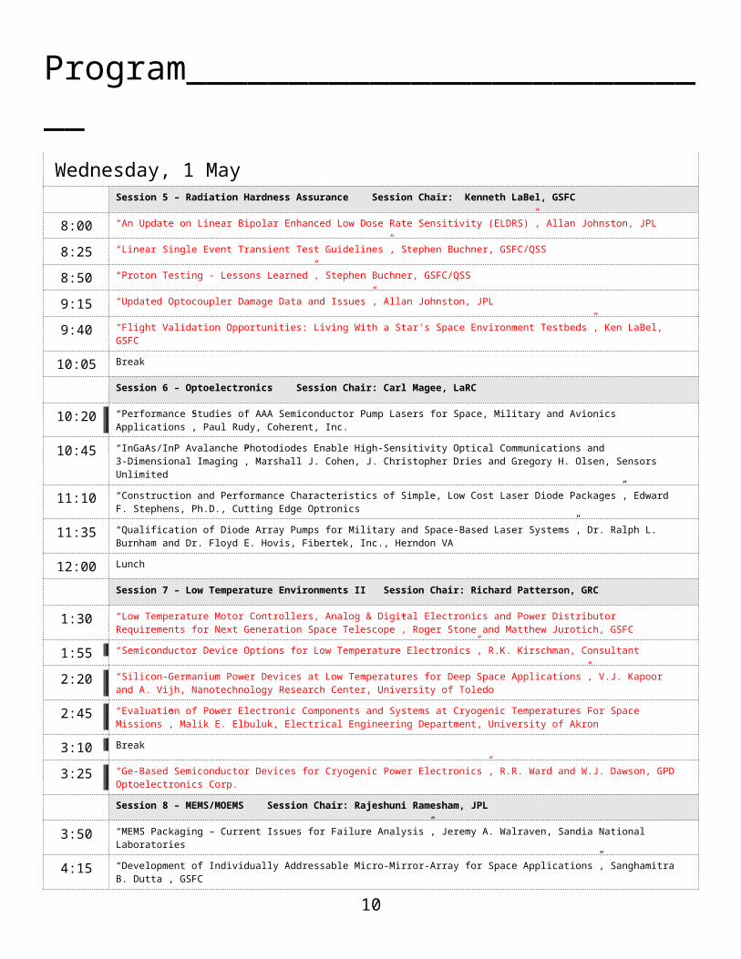
Wednesday, 1 MaySession 5 – Radiation Hardness Assurance Session Chair: Kenneth LaBel, GSFC
8:00 “An Update on Linear Bipolar Enhanced Low Dose Rate Sensitivity (ELDRS)”, Allan Johnston, JPL
8:25 “Linear Single Event Transient Test Guidelines”, Stephen Buchner, GSFC/QSS
8:50 “Proton Testing - Lessons Learned”, Stephen Buchner, GSFC/QSS
9:15 “Updated Optocoupler Damage Data and Issues”, Allan Johnston, JPL
9:40 “Flight Validation Opportunities: Living With a Star's Space Environment Testbeds”, Ken LaBel, GSFC
10:05 Break
Session 6 – Optoelectronics Session Chair: Carl Magee, LaRC
10:20 “Performance Studies of AAA Semiconductor Pump Lasers for Space, Military and Avionics Applications”, Paul Rudy, Coherent, Inc.
10:45 “InGaAs/InP Avalanche Photodiodes Enable High-Sensitivity Optical Communications and 3-Dimensional Imaging”, Marshall J. Cohen, J. Christopher Dries and Gregory H. Olsen, Sensors Unlimited
11:10 “Construction and Performance Characteristics of Simple, Low Cost Laser Diode Packages”, Edward F. Stephens, Ph.D., Cutting Edge Optronics
11:35 “Qualification of Diode Array Pumps for Military and Space-Based Laser Systems”, Dr. Ralph L. Burnham and Dr. Floyd E. Hovis, Fibertek, Inc., Herndon VA
12:00 Lunch
Session 7 – Low Temperature Environments II Session Chair: Richard Patterson, GRC
1:30 “Low Temperature Motor Controllers, Analog & Digital Electronics and Power Distributor Requirements for Next Generation Space Telescope”, Roger Stone and Matthew Jurotich, GSFC
1:55 “Semiconductor Device Options for Low Temperature Electronics”, R.K. Kirschman, Consultant
2:20 “Silicon-Germanium Power Devices at Low Temperatures for Deep Space Applications”, V.J. Kapoor and A. Vijh, Nanotechnology Research Center, University of Toledo
2:45 “Evaluation of Power Electronic Components and Systems at Cryogenic Temperatures For Space Missions”, Malik E. Elbuluk, Electrical Engineering Department, University of Akron
3:10 Break
3:25 “Ge-Based Semiconductor Devices for Cryogenic Power Electronics”, R.R. Ward and W.J. Dawson, GPD Optoelectronics Corp.
Session 8 – MEMS/MOEMS Session Chair: Rajeshuni Ramesham, JPL
3:50 “MEMS Packaging – Current Issues for Failure Analysis”, Jeremy A. Walraven, Sandia National Laboratories
4:15 “Development of Individually Addressable Micro-Mirror-Array for Space Applications”, Sanghamitra B. Dutta , GSFC
4:40 “Multilayered Structures for MEMS Applications”, Arturo A. Ayon, Sony Semiconductor
6
Program___________________________
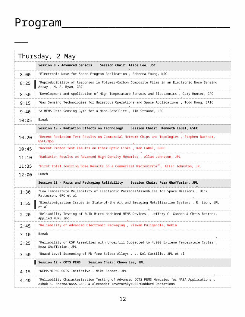
Thursday, 2 MaySession 9 – Advanced Sensors Session Chair: Alice Lee, JSC
8:00 “Electronic Nose for Space Program Application”, Rebecca Young, KSC
8:25 “Reproducibility of Responses in Polymer-Carbon Composite Films in an Electronic Nose Sensing Array”, M. A. Ryan, GRC
8:50 “Development and Application of High Temperature Sensors and Electronics”, Gary Hunter, GRC
9:15 “Gas Sensing Technologies for Hazardous Operations and Space Applications”, Todd Hong, SAIC
9:40 “A MEMS Rate Sensing Gyro for a Nano-Satellite”, Tim Straube, JSC
10:05 Break
Session 10 – Radiation Effects on Technology Session Chair: Kenneth LaBel, GSFC
10:20 “Recent Radiation Test Results on Commercial Network Chips and Topologies”, Stephen Buchner, GSFC/QSS
10:45 “Recent Proton Test Results on Fiber Optic Links”, Ken LaBel, GSFC
11:10 “Radiation Results on Advanced High-Density Memories”, Allan Johnston, JPL
11:35 “First Total Ionizing Dose Results on a Commercial Micromirror“, Allan Johnston, JPL
12:00 Lunch
Session 11 – Parts and Packaging Reliability Session Chair: Reza Ghaffarian, JPL
1:30 “Low Temperature Reliability of Electronic Packages/Assemblies for Space Missions”, Dick Patterson, GRC et al
1:55 “Electromigration Issues in State-of-the Art and Emerging Metallization Systems”, R. Leon, JPL et al
2:20 “Reliability Testing of Bulk Micro-Machined MEMS Devices”, Jeffery C. Gannon & Chris Behrens, Applied MEMS Inc.
2:45 “Reliability of Advanced Electronic Packaging”, Viswam Puligandla, Nokia
3:10 Break
3:25 “Reliability of CSP Assemblies with Underfill Subjected to 4,000 Extreme Temperature Cycles”, Reza Ghaffarian, JPL
3:50 “Board Level Screening of Pb-free Solder Alloys”, L. Del Castillo, JPL et al
Session 12 – COTS PEMS Session Chair: Choon Lee, JPL
4:15 “NEPP/NEPAG COTS Initiative”, Mike Sandor, JPL
4:40 “Reliability Characterization Testing of Advanced COTS PEMS Memories for NASA Applications”, Ashok K. Sharma/NASA-GSFC & Alexander Teverovsky/QSS/Goddard Operations
7

Abstracts and Speaker Info__________Session 1 – High Temperature Environments
New and Emerging Packaging Technologies for Harsh Environments
Robert S. OkojieNASA Glenn Research Center, 21000 Brookpark Road, Cleveland, Ohio 44135, USA.
Abstract
The keys to successful high-temperature Microsystems are the availability of stable high-temperature electronic components (integrated circuits, resistors, capacitors, etc.) and the packaging of these components using the proper materials. The development of silicon carbide integrated circuit (SiC IC) devices for use at temperatures up to 600C has been well underway for these applications. Even though ceramic packages are available for room-temperature electronics, none of them is suitable to package SiC ICs for use over 300oC. Therefore, without parallel developments in packaging technology, the advances in SiC ICs will not much matter. Package selection and development are critical factors in meeting several key requirements: thermal and electrical performance, cost, and form factor.
Critical issues for high temperature (600oC) package include the selection of a package design and package construction materials. Material properties can significantly impact how well the package can meet its requirements. The available materials primarily influence the design of high-temperature packages. This presentation will discuss the high-temperature package design and associated materials issues for SiC devices for use at 600oC.
Speaker Biography
Dr. Robert S. Okojie received the BS, MS and Ph.D. degrees in Electrical Engineering from the New Jersey Institute of Technology in 1991, 1993, and 1996, respectively. He worked at Kulite Semiconductor Products, Inc. from 1993 to 1997 as a Senior Research Scientist involved in implementing the NASA-sponsored program to develop 6H-SiC as a pressure sensor for high temperature applications, which he first reported in January, 1996. He joined Ford Microelectronics, Colorado Springs, CO, in 1997 as a Senior Research Engineer to develop new MEMS sensors, MEMS-based smart fuel injectors, and associated packaging. In June 1999, he joined the SiC research group at NASA Glenn Research Center, Cleveland OH, as an electronics engineer, primarily responsible for developing high temperature ohmic contacts enabling technology for SiC MEMS and electronics. He has published several papers in technical journals and conference proceedings and holds two patents and two pending. He is a member of Sigma Xi, Materials Research Society and IEEE.
High Temperature Reliability of PEMs Using New Molding Compounds
Patrick McCluskey, Arvind Chandrasekaran, Casey O’ConnorCALCE Electronic Products and Systems CenterUniversity of Maryland, College Park, MD 20742Toru Kamei, Sumitomo Corporation Fort Lee, NJ and Anthony Gallo, Dexter Electronic Materials Corp. Olean, NY
Abstract
Over 97% of all integrated circuits produced today are available only in plastic encapsulated, surface mountable, commercial grade or industrial grade versions. This is especially true for the most
advanced technologies. The cost, availability, and functionality advantages of these devices are causing many electronics manufacturers to consider using them in elevated temperature applications such as avionics and automotive under-hood electronic systems to ensure early affordable access to leading edge technology. However, manufacturers only guarantee the operation of commercial devices in the 0C to 70C temperature range, and the industrial devices in the –40C to 85C temperature range.
While previous studies have focused on the ability to use the semiconductor device outside of the datasheet temperature range, this paper describes the first study which addresses the packaging reliability of plastic encapsulated microcircuits (PEMs) in the range from 125C to 300C, well outside the manufacturer’s suggested temperature limits. This study revealed that standard industrial grade plastic encapsulated devices had less than half the lifespan at 180C of similar devices packaged in hermetic ceramic packages. Outgassing of brominated flame-retardants with the associated catalysis of the growth of intermetallics was determined to be the principal cause of failure in the plastic components. Now, however, environmental considerations are leading manufacturers to create bromine-free molding compound formulations that use other techniques to ensure flame retardancy. These new compounds promise removal of this catalytic effect and improved reliability for PEMs at temperatures above 150C. We will discuss the relative availability and reliability of components packaged in these new compounds, along with studies conducted on 84-lead PQFP leadframes encapsulated in two different molding compounds that revealed that the bromine-free plastic encapsulant itself begins to lose its ability to insulate leads at temperatures greater than 250C and can actually combust at temperatures greater than 300C.
Speaker Biography
Patrick McCluskey is an Assistant Professor of Mechanical Engineering at the University of Maryland, College Park where he is associated with the CALCE Electronic Products and Systems Center. He is the principal investigator for projects related to packaging and reliability of electronic components in high power and high temperature environments. He has co-developed and taught graduate level and executive short courses on high temperature electronics, power electronics packaging, and plastic encapsulated microelectronics. He is the author or co-author of over 50 journal and proceedings articles on his research, and the co-author of two books on electronic packaging including High Temperature Electronics. Dr. McCluskey received his Ph.D. in Materials Science and Engineering from Lehigh University in 1991. He is a member of IEEE, IMAPS, ASM, ECS, and MRS.
Structure Optimization of Wire-bond for High Temperature Operation
Shun-Tien Lin, Hamilton-Sundstrand Corp., Tel: 860-654-9205 Email: [email protected] Luo, United Technologies Research Center
Abstract
Wire-bonds provide electrical connection between die and bond pads in microelectronic packages. The wire-bond is subjected to stresses during the operating life as a result of temperature and/or power cycling. Failure of the wire bond occurs predominantly as a result of thermo-mechanical fatigue. The dominant failure mechanism will depend on the operating environment, the wire, wire-bond and pad materials and the geometry of the wire and the wire bond. The wire-bond reliability is one of the major concerns for high temperature applications. The objective of this work was to determine the most
8

Abstracts and Speaker Info__________reliable wire-bond system for high temperature applications. Design optimization approach was considered in this investigation to obtain reliable wire bond system. Parametric finite element models have been developed for gold wire and wedge-type wire-bond system. The finite element model was then interfaced with an optimization tool. Six design variables were selected and strains at potential failure locations were optimized. This presentation will summarize the methodology and the optimized results.
Speaker Biography
Shun-Tien (Ted) Lin received the Ph.D. in Engineering Mechanics from University of Wisconsin-Madison, the M.S. in Mechanical Engineering from Auburn University, and the B.S. in Mechanical Engineering from Feng Chia University in Taiwan. His areas of interests include electronics packaging reliability prediction, piezoresistive stress sensor technologies, and computational and experimental mechanics. Currently, he is a Sr. Engineer at the Hamilton-Sundstrand Corp.
9
Abstracts and Speaker Info__________Session 2 – Low Temperature Environments I
Ceramic Temperature Operation over Extreme Temperatures
Elaine Gee, Muses-CN Nanorover Project, JPL
SOI Device Optimization for Low Temperature and Radiation Tolerance
Jagdish Patel, JPL, John Cressler, Ying Li, Auburn University
Hot Carrier Degradation Effects in Power MOSFETs Operating at Cryogenic Temperatures
Elaine Gee and Michael Newell, JPL
Chip On Board, a path to Extreme Temperature Operation of Space Electronics
Ken Hicks, JPL
10

Abstracts and Speaker Info__________Session 3 – LaRC-MFC Technology
Overview of NASA-Langley Macro-Fiber Composite (MFC) Piezoelectric Actuator Technology
W. Keats Wilkie
Army Research Laboratory; NASA Langley Research Center [email protected]: 757/864-1260 FAX: 757/864-8808
Abstract
The Macro-Fiber Composite actuator (MFC) is a high performance piezoelectric composite device developed by NASA Langley Research Center and the Army Research Laboratory. The MFC was initially created to control vibrations and deformations in composite helicopter rotor blades. It has since found use in a wide range of uses, in particular, with inflatable-rigidizable composite spacecraft applications. The MFC's features include high work output, low weight, low power requirements, low manufacturing cost, and repeatable properties and performance. An overview of the design history, manufacture, and performance testing of the MFC actuator device will be presented here. A summary of ongoing MFC applications research will also be given.
Speaker Biography
Keats Wilkie received a B.S. in applied physics from the University ofAlabama in 1986. He holds an M.S. degree in Engineering Science and Mechanics from the Georgia Institute of Technology (1990), and M.S. and Ph.D. degrees in Aerospace Engineering Sciences from the University of Colorado at Boulder (1995, 1997). He has been a research aerospace engineer with the U.S. Army Research Laboratory, and detailed to NASA Langley Research Center, since 1986. His research areas include structural dynamics and control, rotary wing dynamics, and active structures and actuator design. He currently leads NASA-Langley's Macro-Fiber Composite Actuator development efforts.
Design and Characterization of Radial Field Diaphragms
Robert G. BryantNASA Langley Research CenterMS 226, Hampton, VA 23681
Abstract
Radial Field Diaphragms “RFD” are NASA Langley’s latest piezoelectric ceramic actuators. The RFD uses an in-situ radial electric field to displace a piezoelectric element along the Z-axis (out of plane). The unique feature of these actuators is that they display concentric deformation and thus, are not benders. This allows these diaphragms to be mechanically constrained about their perimeter without dramatically affecting their performance. The fabrication of these diaphragms is based on that of NASA’s Macrofiber Composite ”MFC” (currently under NEPP evolution). This talk will focus on the ongoing selection criteria, fabrication process, basic characterization and initial results of these RFDs prior to higher-level evaluation required for potential mission support. There are several uses for this new type of actuator including sonic transducers, diaphragm pumps, active valves and dynamic sensors.
Speaker Biography
Robert G. Bryant received a BS in Chemistry with minors in Math and Physics from Valparaiso University in 1985. He graduated from
the University of Akron with an MS (1990) and a Ph.D. (1995) in Polymer Science under an NASA GSRP fellowship. Since 1990, he has been employed at NASA Langley Research Center as a Senior Chemical Engineer in the Advanced Materials and Processing Branch. His current research interests include the development of smart materials and subsystems, new material hybrids, fabrication technology, and material concepts for electronics. Dr. Bryant holds over 15 patents, approximately 50 publications, and has several licensed inventions. He has earned three NASA Group Achievement Awards, the NASA Holloway, Whitcomb, and TGIR, the Medal of Exceptional Achievement, three R&D 100 Awards (including editor's choice), and the Valparaiso University Alumni Achievement and Outstanding Young Alumni Awards. Currently, he holds adjunct professorships at the College of William and Mary, Virginia Tech, and Virginia Commonwealth University. Professional memberships include the American Chemical Society (ACS) and IMAPS. Additional Information:Dr. Robert G. BryantNASA Langley Research CenterResearch and Technology CompetenciesStructures and Materials CompetencyAdvanced Materials and Processing BranchMail Stop 2266 West Taylor StreetHampton, VA 23681-2199Phone: 757-864-4262Fax: 757-864-8312E-mail: [email protected]
Reliability Testing of MFC Actuators
James W. High 3 , W. K. Wilkie2, and James F. Bockman1
NASA Langley Research CenterMS 4881, 2302, 3903
Hampton, VA 23681
Abstract
NASA Langley Research Center (LaRC) has developed Micro-Fiber Composite (MFC) actuators as a core enabler to control vibrations in extremely large inflatable smart space structures, next generation space telescopes, etc. Test show that the LaRC-MFC actuator is capable of producing large, directional in-plane strains, on the order of 2000 parts-per-million (ppm). Preliminary ambient endurance testing indicates that the device is durable, with no reductions in free-strain performance to at least 100 million electrical cycles. This paper describes methods, measurements, and results for our reliability evaluation of the LaRC-MFC under strained conditions.
Speaker Biography
James W. High is currently assigned to the Electronics Applications Technology Branch at NASA Langley Research Center. He is a 1996 graduate of the NASA Technical Apprentice School. He received an Associate in Applied Science (AAS) degree in Electronics from Thomas Nelson Community College in 1994. Prior to coming to work for NASA, Mr. High was employed as a licensed Master electrician.
Miniaturizing High Voltage Amplifiers for Piezoelectric Actuators
By Paul Robinson and James Bockman, LaRC
Abstract
11
Abstracts and Speaker Info__________NASA Langley Research Center (LaRC) is developing miniature high voltage amplifiers for piezoelectric actuator use. Several small amplifiers have already been built. Our goal is to miniaturize the amplifiers to the point that they can be integrated onto the actuator package. Many aerospace applications cannot tolerate the typically large, by size and weight, commercial high voltage power supplies. An output voltage range of +/-500Vpeak to +/- 1500Vpeak amplifiers are being developed which are small and can be distributed throughout a structure. These are power amplifiers and internal dissipation is a major concern for miniaturization. Thermal constraints impose the harshest obstacle to amplifier miniaturization. To overcome thermal dissipation issues the only circuit topology that will work is class “D”. Transistor voltage issues are another severe limiter to direct high voltage amplifier design. The current state of the art in transistors is about 1500 volts. This means that the maximum peak-to-peak amplifier output swing is half or about 750 volts. For an amplifier to have a larger output swing the linear designer has to resort to various techniques to increase the output voltage swing. One technique is to bridge two amplifiers together. This will result in doubling the output voltage swing to a maximum of 1500 volts. Another technique is to use a “series” string of transistors to increase the output voltage swing. The voltage issues can be overcome by locating the high voltage in an output transformer and filter in a switching amplifier. This will result in an amplifier that has a small footprint, low dissipation requirements (small or no heat sink), light weight and low cost. The volumetric efficiency in a class “D” is dense enough to realize the goal of integrating an amplifier onto an actuator package.
Speaker Biography
Paul C. Robinson is an electrical engineer with Science Applications International. He has been in the electronics industry for over 20 years. He is currently developing several custom high voltage electronics designs. He was born in Arlington Virginia. He has lived in the tidewater area of Virginia for over 30 years. He is a graduate of Old Dominion University School of Engineering (BS ’00).
12
Abstracts and Speaker Info__________Session 4 – Innovative Qualification and Test Methods
Fiber Optic Cable Assembly Characterization Studies at NASA Goddard Space Flight Center
Melanie N. OttSigma Research and Engineering / NASA Goddard Space Flight CenterComponent Technologies and Radiation Effects [email protected]
Abstract
In the past, space flight specifications for optical fiber cable assemblies required a long list of qualification tests. Since the usage of commercial products became an acceptable practice and a necessity for space flight, this long list of qualification testing became impractical. This was due to the vast time consumption and high cost expenditures for vendors and space flight projects to perform these testing plans each time that a part or process was changed or an alternative design was necessary. This change in scope and the advances in fiber optic technologies required more focus be placed on the methods by which cable assemblies were characterized. The goal was to identify new test plans that could be used to bring out failure modes of the parts and packaging but with fewer required tests, of less duration. In the past five years, the GSFC Technology Validation Assurance Laboratory for Photonics has focused on this issue for NEPP. A thorough investigation was conducted on failure modes and testing to advance aging on optical fiber assemblies.[1] The objective was to eliminate unnecessary testing that had become entrenched in the specification process through heritage but that did not necessarily provide reliability information specific to space flight environments. The result of this study allowed for new test plans to be formulated. These test plans have been used to validate several types of cable assembly technologies that were not previously available for space flight.[2-6] Other heritage technologies have been made obsolete as the study uncovered failure modes that now could be identified more readily through innovative characterization test methods.[2,4]This presentation will provide a summary, with recent examples, of the effort to provide innovative characterization plans that minimize cost but allow for reliability assessments on commercial optical fiber cable assemblies for space flight environments.
1. Melanie Ott, Jeannette Plante, Fiber Optic Cable Assemblies for Space Flight Applications: Issues and Remedies, SAE/AIAA publication, World Aviation Congress, October 1997.
2. Melanie Ott, Fiber Optic Cable Assemblies for Space Flight II: Thermal and Radiation Effects, :July 1998, SPIE Proceedings Vol. 3440 Photonics for Space Environments.
3. Melanie Ott, Joy Bretthauer , Twelve Channel Optical Fiber Connector Assembly: From Commercial off the Shelf to Space Flight Use, July 1998, SPIE Vol. 3440 Photonics for Space Environments.
4. Melanie Ott, Patricia Friedberg, Technology Validation of Optical Fiber Cables for Space Flight Environments, SPIE Proceedings Vol. 4216, Optical Devices for Fiber Communication II, Conference November 8, 2000.
5. Matthew Bettencourt, Melanie Ott, Fiber Optic Epoxy Outgassing Study for Space Flight Applications , NEPP Web Publication, October 4, 2001.
6. Melanie Ott, Shawn Macmurphy, Patricia Friedberg, Characterization of a twelve channel optical fiber, ribbon cable and MTP array connector assembly for space flight environments, SPIE Proceedings Vol. 4732, Enabling Photonic Technologies for Aerospace and Applications IV, 2002.
Speaker Biography
Melanie N. Ott is a Principal electrical systems engineer from Sigma Research and Engineering and functions as the Director of the photonics laboratories for the Component Technologies and Radiation Effects Branch at NASA Goddard Space Flight Center. Under her leadership, the laboratories support NASA projects from design to integration and testing for applications of photonic systems for communications, LIDAR and sensing systems. She has published thirty seven papers, articles and presentations on the subject of photonics for space flight most of which are available on the Code 562 photonics website. For NEPP, Ott has focused on the reliability of fiber optic and photonic component packaging and parts for the past seven years.
Ott holds a Masters in Electrical Engineering with Optics emphasis from Virginia Polytechnic Institute and State University. Prior to working at GSFC she worked at NASA Langley Research Center, the Fiber and Electro Optics Research Center (FEORC) in Blacksburg Virginia and the Crystal Physics Laboratory at the Massachusetts Institute of Technology.
Rapid Qualification of Area Array Package Assemblies by Increase of Ramp Rates and Temperature Ranges
Reza GhaffarianJet Propulsion Laboratory, California Institute of Technology , Pasadena, [email protected], (818) 354-2059
Abstract
Advanced area array packaging, including brought about new package technology including materials and processes as well new applications with environmental requirements not seen in their previous generation. Rapid insertion of electronics packaging technology necessitates faster qualification implementation and therefore development of accelerated test methods. Increase of ramp rate up to 20°C/min is allowed in a recently released specification, IPC 9701, “Performance Test Methods and Qualification Requirements for Surface Mount Solder Attachments”.
Accelerated thermal cycling with a large temperature swing can be used as an environmental screening test and often has been considered as a qualification requirement for harsh environmental applications. There are many concerns, however, when such accelerations are performed especially for electronics packages with no environmental testing heritage. These concerns include: the effects of cold and hot temperatures in a cycle range, time and temperature at dwells, temperature exposure to higher than 110°C for eutectic solder, and the effects of heating/cooling rates.
A JPL-led chip scale package (CSP) Consortium of enterprises, composed of team members representing government agencies and private companies, have joined together to pool in-kind resources for developing the quality and reliability of chip scale packages (CSPs) for a variety of projects. The Consortium assembled fourteen different area array packages from 48 to 784 I/Os and pitches from 0.5 to 1.27 mm on multilayer FR-4 printed wiring boards (PWBs). A leaded package was used as control. In addition, two other test
13

Abstracts and Speaker Info__________vehicles built by two team members, each had a control wafer level CSP package for data comparison. To meet various qualification needs of team members, assemblies were subjected to thermal cycling ranges representative of military, space, and commercial. The most rapid qualification was performed using thermal cycling in the range of 55 to 125°C with a near thermal shock ramp rates. Cycles-to-failure (CTF) test results to 3,000 cycles performed under this and three other thermal cycling ranges including 0 to 100° C are presented. The effect of ramp rate increase on CTFs and failure mechanisms for thermal cycling performed under near thermal shock and thermal cycle in the range of -55 to 125°C are also presented.
Speaker Biography
Dr. Reza Ghaffarian has 20 years of industrial and academic experience in mechanical, materials, and manufacturing process engineering. At JPL, Quality Assurance Section, he supports research and development activities in SMT, BGA, CSP, and MEMS/MOEMS technologies for infusion into NASA’s missions. He was the recipient of NASA Exception Service Medal for outstanding leadership, industrial partnering, and expertise in failure modes and effects analysis and environmental testing of electronic packaging technologies. He has authored more than 100 technical papers, co-editor of a CSP book, 3 book chapters, two guidelines, and numerous patentable innovations. He serves as technical advisor/Committee to Chip Scale Review Magazine, Microelectronics Journal, SMTA, IMAPS, and IPC. He is a frequent speaker and chaired technical conferences including SMTA International, IMAPS, ASME, SAMPE, NEPCON, SEMI, IEEE CPMT, and IPC. He received his M.S. in 1979, Engineering Degree in 1980, and Ph.D. in 1982 in engineering from University of California at Los Angeles (UCLA).
Qualification of SoC for Spacecraft Avionics Applications
Jonathan Perret, JPL
Abstract
SoC devices require different approaches to the qualification process in order to address: the device complexity, integration of design elements of different forms, embedded memory elements, embedded software, the inclusion of analog elements and the difficulty in attaining test access. This paper presents an approach to meeting these challenges for spacecraft avionics applications.
Speaker Biography
Jonathan Perret earned a B.S. in Electrical Engineering at California State University Polytechnic, Pomona in 1980, and a M. S. in Electrical Engineering at California State University, Los Angeles, in 1982. He developed spacecraft radio hardware at JPL producing hardware for the Galileo, Cassini, and Mars Pathfinder spacecraft. Currently, he is working to establish the development processes for SoC devices planned for use in spacecraft applications.
Characterization of Integrated Fiber Optical Modulators for Space Flight
Melanie N. OttNASA Goddard Space Flight Center / Sigma Research and EngineeringComponent Technologies and Radiation Effects [email protected]
Abstract
This presentation will provide status-to-date on the NEPP task focused on the reliability of optical modulators, including failure modes and innovative characterization techniques that will be used to enable the space flight usage of this commercial technology.Optical modulators are of great interest to space flight projects for communications and LIDAR applications. This study focuses on the reliability of commercially available optical fiber modulators for space flight environments. It is well known that space flight projects have a unique set of requirements rarely accommodated by industry standards. Space flight power budgets are typically stringent and low, and space flight thermal environments can cause premature aging. In order to use commercial telecommunications technology and take advantage of the state-of-the-art available, a thorough understanding of the technology must be attained such that risk assessments can be conducted. One way of accomplishing this goal of balancing between usage of advanced commercial technology while still maintaining a highly reliable system is to focus on understanding the potential failure modes associated with this technology.The first phase of this study on optical modulators focuses on explaining the failure modes of these devices for ground based and space flight systems. In addition to identifying the failure modes, this research will provide insight into which devices currently available incorporate designs that mitigate against failure or degradation. The devices that have the greatest potential for survival in a space flight environment are being identified, based on the results of this study. The second phase of this investigation focuses on the characterization techniques used to bring out the failure modes of optical modulators. Commercial testing methods used in the past for characterization are very time consuming and require highly expensive equipment. The objective is to provide innovative testing and characterization methods that incorporate the intention of test methods used in the past without the long duration and expensive equipment requirements. Using these test methods the components identified in phase one of this study will be evaluated and characterized for usage in a space flight environment.
Speaker Biography
Melanie N. Ott is a Principal electrical systems engineer from Sigma Research and Engineering and functions as the Director of the photonics laboratories for the Component Technologies and Radiation Effects Branch at NASA Goddard Space Flight Center. Under her leadership, the laboratories support NASA projects from design to integration and testing for applications of photonic systems for communications, LIDAR and sensing systems. She has published thirty seven papers, articles and presentations on the subject of photonics for space flight most of which are available on the Code 562 photonics website. For NEPP, Ott has focused on the reliability of fiber optic and photonic component packaging and parts for the past seven years.
Ott holds a Masters in Electrical Engineering with Optics emphasis from Virginia Polytechnic Institute and State University. Prior to working at GSFC she worked at NASA Langley Research Center, the Fiber and Electro Optics Research Center (FEORC) in Blacksburg Virginia and the Crystal Physics Laboratory at the Massachusetts Institute of Technology.
14

Abstracts and Speaker Info__________Session 5 – Radiation Hardness Assurance
An Update on Linear Bipolar Enhanced Low Dose Rate Sensitivity (ELDRS)
Allan Johnston, JPL
Linear Single Event Transient Test Guidelines
Stephen Buchner, GSFC/QSS
Proton Testing - Lessons Learned
Stephen Buchner, GSFC/QSS
Updated Optocoupler Damage Data and Issues
Allan Johnston, JPL
Flight Validation Opportunities: Living With a Star's Space Environment Testbeds
Ken LaBel, GSFC
15
Abstracts and Speaker Info__________Session 6 – Optoelectronics
Performance Studies of AAA Semiconductor Pump Lasers for Space, Military, and Avionics Applications
Paul Rudy, Ph.D.Coherent, Inc.Santa Clara, CA
Abstract
The development of aluminum-free semiconductor laser technology at Coherent, Inc. has resulted in commercially available, long-lived, pump laser devices and arrays. This talk will focus on the Aluminum-free in the Active Area (AAA) semiconductor laser technology of Coherent Semiconductor Division, focusing on its advantages in the demanding space, military and avionics environments. An overview of the AAA material will be presented including a discussion of the performance of present products, and the progress to date on new wavelengths and advanced packages for increased performance and reliability.
Speaker Biography
Paul Rudy, Ph.D. is the Market Development Manager for pump lasers at Coherent, Inc. He has previously served as the Product Manager at Coherent Semiconductor Group, and as the Mid-Atlantic Scientific Sales Engineer for Coherent Semiconductor Group and Coherent Laser Group. He received his doctoral degree in atomic physics at the University of Rochester.
InGaAs/InP Avalanche Photodiodes Enable High-Sensitivity Optical Communications and 3-Dimensional Imaging
Dr. Marshall J. Cohen, Dr. J. Christopher Dries, and Dr. Gregory H. Olsen, Sensors Unlimited, Inc., Princeton, NJ
Abstract
The maturation of III-V compound semiconductor device fabrication is enabling the widespread use of previously exotic optical components and modules. In this talk we discuss recent advances in InGaAs/InP avalanche photodiode growth and processing, and introduce some new applications where these devices may be used.
Avalanche photodiodes (APDs) provide current gain for receivers in optical communication systems and are the detector of choice for high sensitivity laser range finding. Photodiode current gain results in dramatically improved sensitivities (as much as 10dB) for the receivers used in both applications. Arrays of InGaAs APDs enable eye-safe, covert 3-Dimensional imaging for laser range finding systems in the 0.9 – 1.7 micron wavelength band. These imagers provide target recognition as well as range information, enabling more sophisticated next generation weapons systems.
Until recently, APDs were thought to be expensive, unreliable, and difficult to operate. In reality, we are achieving unprecedented device yields that allow us to manufacture receivers at a modest cost premium over pin based receivers while achieving 6-10 dB better sensitivity. Furthermore, APDs enjoy the same geologic lifetimes as pin diodes. Current reliability studies (4000 hours) show no device failures at 200C under 40 volts reverse bias. The miniaturization of bias and control electronics greatly simplifies the support electronics required to run APDs. Available circuits provide active temperature compensation, and are enabling APD deployment in inexpensive datacom transceivers. Finally, APD based receivers are also finding
utility in free-space optical communication systems, whether they are building to building, or from satellite to satellite systems.
Speaker Biography
Marshall Cohen has been Executive Vice President at Sensors Unlimited, Inc. since 1993, spearheading the development of InGaAs FPAs and cameras. Since October 2000, Sensors Unlimited has been a division of Finisar, Inc. and has emphasized the development of high speed avalanche and PIN photodiodes for optical communications. Before Joining Sensors Unlimited, be was Business Element Manager at EG&Gs Princeton Applied Research responsible for optical multichannel analyzers and Section Manager at Rockwell International’s Science Center responsible for GaAs CCDs. Dr. Cohen received his Ph.D. in Solid State Physics in 1975 from the University of Pennsylvania.
Construction and Performance Characteristics of Simple, Low Cost Laser Diode Packages
Edward F. Stephens, Ph.D.
Director of Product DevelopmentSemiconductor DivisionCutting Edge Optronics20 Point West Blvd.St. Charles, MO 63301636-916-5656 ext. 204
Abstract:
High power laser diode bars have been packed in many different configurations over the past several decades. Cutting Edge Optronics has developed. several packages designed for low cost, high volume production. The performance characteristics of several conductively cooled as well as water cooled packages will be presented and compared. Data from a high power laser diode array cooled with individual microchannel coolers will also be examined.
Speaker Biography
Dr. Edward Stephens graduated with a B.S. and M.S. in Physics from Southern Illinois University at Edwardsville. His M.S. thesis focused on the computational modeling of high power laser diode bars. He graduated with a doctorate in Physics from University of Missouri at Rolla (UMR). Part of his Ph.D. thesis work was performed at McDonnell. Douglas Corporation we be experimentally investigated developing high power laser diode arrays. Addition research was done at UMR developing tunable solid-state lasers. Dr. Stephens has been with CEO's Semiconductor Laser Division since its inception in 1996. He was a key contributor to the development of CEO's laser diode array packages as well as the production setup for those packages.
Qualification of Diode Array Pumps for Military and Space-Based Laser Systems
Dr. Ralph L. Burnham and Dr. Floyd E. Hovis, Fibertek, Inc.
Over the past 10 years Fibertek has designed, manufactured, qualified, and fielded numerous high-performance diode-pumped solid-state laser-based systems for field use. Examples of ground and helicopter based systems include laser transmitters for the navy Magic Lantern and other underwater detection systems on SH-53 and SH-60 helicopters, the army Obstacle Avoidance System (OASYS) helicopter laser radar on UH1H helicopters, the Biological Standoff Detection Systems on UH-60 helicopters and HMMV
16

Abstracts and Speaker Info__________ground transport vehicles, and the Northrop-Grumman Viper IRCM laser transmitters on UH-60 helicopters. Systems designed for use in space include the laser transmitters for the Vegetation Canopy Lidar (VCL) and the CALIPSO-CENA aerosol lidar system. The Viper systems built for Northrop Grumman Corporation are currently in the E&MD phase and the laser transmitters for CALIPSO-CENA are currently undergoing final flight qualification. These two systems each had their own unique and stressing system level requirements. The Viper systems are designed for the diodes to be operated at a heat sink temperature of 70°C in ambient environments that ranged from -54°C to +70°C. The CALIPSO-CENA mission will have a relatively benign thermal environment, but the laser transmitter must survive over 10 grms random vibration levels and operate near continuously for three years on orbit and over 2 billion shots. We will discuss the approaches taken and difficulties encountered in the qualification of the pump diode arrays for these stressing environments.
Speaker Biographies
Dr. Ralph Burnham is a Senior Vice president of Fibertek, Inc. with over 25 years experience in the fields of laser physics and optics. At Fibertek, Inc. Dr. Burnham has concentrated on the development of high-power solid-state lasers for military and commercial applications. His work in this area includes the design, development and qualification of lasers for aircraft and space-based lidar and remote sensing systems. His research group at Fibertek have qualified and flown the highest power diode-pumped solid-state lasers to date.
Dr. Floyd Hovis is Director of Space Lasers at Fibertek, Inc. and has over 20 years of experience in research in laser physics and chemistry as well in the design and production of hardened laser systems. At Fibertek he has been actively involved in the qualification of lasers for use in hostile environments on a number of military and space-based programs. He has a particular in the in the development of the contamination control techniques required for long-term, sealed operation of laser transmitters.
17
Abstracts and Speaker Info__________Session 7 – Low Temperature Environments II
Low Temperature Motor Controllers, Analog & Digital Electronics and Power Distributor Requirements for Next Generation Space Telescope
Roger Stone and Matthew Jurotich: Next Generation Space Telescope, NASA Goddard Space Flight Center, Greenbelt, MD 20771
Abstract
Speaker Biography
Semiconductor Device Options for Low Temperature Electronics
R.K. Kirschman: Consulting Physicist, Mountain View, CAR.R. Ward: GPD Optoelectronics Corp., Salem, NHAbstract
Speaker Biography
Silicon-Germanium Power Devices at Low Temperatures for Deep Space Applications
V.J. Kapoor and A. Vijh: Nanotechnology Research Center, University of Toledo, OH 43606R.L. Patterson and J.E. Dickman: NASA Glenn Research Center, Cleveland, OH 44135
Abstract
Speaker Biography
Evaluation of Power Electronic Components and Systems at Cryogenic Temperatures For Space Missions
Malik E. Elbuluk: Electrical Engineering Department, University of Akron, OH 44325 Ahmad Hammoud: QSS Group, Inc., NASA Glenn Research Center, Cleveland, Ohio 44135Scott S. Gerber: ZIN Technologies, NASA Glenn Research Center, 3000 Aerospace Parkway, Brook Park, OH 44142Richard L. Patterson: NASA Glenn Research Center, Cleveland, OH 44135Ashok Sharma, NASA Goddard Space Flight Center, Greenbelt, MD
Abstract
Speaker Biography
Ge-Based Semiconductor Devices for Cryogenic Power ElectronicsR.R. Ward and W.J. Dawson: GPD Optoelectronics Corp., Salem, NHR.K. Kirschman: Consulting Physicist, Mountain View, CAO. Mueller: LTE – Low Temperature Electronics, Ballston Lake, NYR.L. Patterson and J.E. Dickman: NASA Glenn Research Center, Cleveland, OH 44135A. Hammoud: QSS Group, Inc., NASA Glenn Research Center, Cleveland, OH 44135
Abstract
Speaker Biography
18
Abstracts and Speaker Info__________Session 8 – MEMS/MOEMS
MEMS Packaging – Current Issues for Failure Analysis
Jeremy A. WalravenSandia National Laboratories, Albuquerque, NM
Abstract
Packaging of microelectromechanical systems (MEMS) poses major technical issues for package and failure analysis engineers. Conventional IC’s are packaged with the intent to dissipate heat, distribute electrical signals and power, and provide overall protection from external influences. Packaged MEMS components must provide the same heat dissipation, power and electrical distributions, but have direct interaction with the surrounding environment. The MEMS and its environment may consist of various chemicals (chemical sensor), large gap spacings in ambient atmosphere (accelerometer), optically transparent-hermetically sealed systems (optical sensors and switches), ink/dye and medicinal transport (microfluidic drop ejectors and systolic pumps). These devices perform some sort of mechanical function ranging from switching optical signals, sensing changes in acceleration, and pumping nanoliters of fluid.
In MEMS packaged devices, the challenges facing the failure analyst include performing non-destructive structural, electrical, and chemical analysis, and package disassembly without introducing any change in the environment that would affect the component environment and hence a different failure mechanism. This presentation will discuss the some of the current packaging issues, but focus primarily on the failure analysis difficulties associated with packaged MEMS.
Speaker Biography
Jeremy A. Walraven received his Masters in Materials Science and Engineering from North Carolina State University in 1998. Sandia National Laboratories employed him in 1998 as a failure analyst working on MEMS, optoelectronics and microelectronics. Mr. Walraven is currently the lead MEMS failure analyst focusing on establishing root cause failure mechanisms, their impact on reliability, and provides corrective action to eliminate the failure modes.
Development of Individually Addressable Micro-Mirror-Array for Space Applications
Sanghamitra B. Dutta NASA, Goddard Space Flight Center, Code 553, Greenbelt, MD 20771
Abstract
A two dimensional array of individually addressable Micro-Mirror-Array (MMA) with large angle of deflection (±100) has been developed at NASA, GSFC for possible application in space and ground based astronomy including the Next Generation Space Telescope (NGST). MEMS technology permits the construction of Micro-Mirror-Arrays (MMA) with self-contained actuation mechanisms and direct interfaces to digital electronics. These devices have low mass and power requirements, and can be constructed with high reliability at relatively low cost, making them attractive for future space applications. We have designed and successfully fabricated a 32x32 array of MMA by using standard surface micro-machining technique at the Detector Development Laboratory (DDL) at GSFC. The 100micronx100micron single pixel
aluminum micro-mirrors are built on top of CMOS driven address and driver circuit for individual addressing. The tilting of the mirrors is achieved by electrostatic attraction between two parallel plate aluminum electrodes. A pair of thin aluminum torsion straps is used so that the voltage required for tilting is less than 20V. The array has been tested successfully to operate at room temperature and at 30K for over 106 cycles. Model operation of mirror elements has been simulated extensively. Experimental data are in good agreement with model predictions. For optimal operation of MMA, different alloy materials were studied for mirror fabrication. Electro-mechanical modeling, material property studies, fabrication, packaging and optical characterization of the MMA will be presented in detail. Data at room temperature and at cryogenic temperature will be presented.
Speaker Biography
Dr. Sanghamitra (Mitra) Dutta is a senior member of the engineering staff at NASA, Goddard Space Flight Center. She has been working in the area of semiconductor detectors, accessories and MEMS research and development at NASA for the past nine years. She has developed the first two-dimensional array of silicon micro-calorimeters for X-ray spectroscopy for ASTRO-E flight program. She has developed several MEMS devices for different flight projects in collaboration with the Photonics, Cryogenics and Solar physics Branches at GSFC. She has led a team that developed and demonstrated the operation of individually addressable 32x32 array of micro-mirrors at room-temperature and at cryogenic temperature for the NGST-MEMS technology development. She received her Ph.D. in physics from the University of Rochester, NY. Prior to joining NASA she worked in major US and European Universities and National laboratories and contributed in fundamental physics research area.
Multilayered Structures for MEMS Applications
Arturo A. Ayon, Ph.D.MEMS Business Development Manager
Sony Semiconductor1 Sony PlaceSan Antonio, TX 78245-2100Telephone: (210) 647-6272Fax: (210) 647-6915Email: [email protected]
Abstract
The number of MEMS projects employing silicon wafer laminations has increased dramatically in recent years thanks to the advent of deep reactive ion etching (DRIE) and a better understanding of the wafer bonding process. Challenging applications including micro-rockets, micro-combustors, micro-turbine engines and other structures for propulsion, power generation and space exploration are presently being demonstrated. However, many issues have not been adequately resolved that either limit the performance of current devices or preclude the development of new and more complicated structures. Specifically, for dry etching of potentially useful materials and ceramics, silicon remains the only option for which there is readily available commercial equipment offering both high etching rates and good selectivity even to polymers. Nevertheless, even in the case of silicon a number of issues still have to be dealt with during micro-processing, namely, aspect ratio dependent etching (ARDE), etching-induced surface roughening and loss of profile control. For other materials dry etching capabilities are limited or nonexistent. When employing wafer bonding, surface roughness, surface contamination and wafer-to-wafer alignment are always critical and the fabrication of structures involving more than one
19
Abstracts and Speaker Info__________ceramic material is difficult due to stresses in deposited films and severe mismatches in the coefficients of thermal expansion. Additionally, the deposition of diverse materials presents challenges in terms of deposition speed, the attainable microstructure and the surface roughness of the resulting films. We review the issues involving silicon and other ceramics and suggest potential solutions.
Speaker Biography
20
Abstracts and Speaker Info__________Session 11 – Advanced Sensors
Electronic Nose for Space Program Application
Rebecca Young, NASA Kennedy Space CenterWilliam J. Buttner, Dynacs Corp, Kennedy Space CenterRajeshuni Ramesham, Jet Propulsion Laboratory
Abstract
The ability to ensure the health and safety of astronauts is important. A lightweight, low power, miniature instrument capable of real-time monitoring of chemical contaminants at trace levels is needed for the Shuttle and the International Space Station. There are two specific applications that are currently being investigated. (1) To monitor air contaminants in the crew cabin for providing notification of sudden adverse events, such as fire, spills, or leaks. (2) To monitor for hypergolic propellant vapors in the airlock after astronauts’ space walk to ensure the toxic vapors would not be brought into the crew cabin.
The Electronic Nose uses an array of non-specific sensors, in which the pattern and magnitude of response induced by an air sample across the sensors are used to identify and quantify the contaminants. The electronic Nose can "sniff" to detect a change in the environment. It can also be trained to identify the contaminant that causes the change.
At NASA Kennedy Space Center, several electronic nose instruments, each with different sensor array designs, are being evaluated for these applications. The presentation will describe the laboratory equipment setup, test protocol, and discrimination power of the various electronic nose technologies. The critical performance parameters include detection limit, dynamic range, response time, humidity/temperature and ambient pressure effects, and stability. The presentation will also describe the use of the Electronic Nose for the detection of pre-combustion fire due to overheating of electrical wires. The results will demonstrate the applicability of electronic nose instrument for the space program.
Speaker Biography
Rebecca Young received a MS degree in Chemistry from University of Texas, Austin, Texas and also a MS degree in Engineering Management from University of Central Florida, Florida. She is currently serving as the Lead of Chemical Instrumentation Group at NASA-KSC. Her responsibilities include: manage the infrastructure of the Applied Chemistry Laboratory to support various research and development projects; Develop and evaluate hypergolic vapor detectors, pre-combustion fire alarm, air quality and event monitors using GC-MS and electronic nose technologies, and others; Formulate specification and acceptance test procedures for new vapor detectors for use at KSC.
Rebecca has previously served as Chief of the Environmental Operations Office, Clean Air Program Manager, and Manager of KSC Toxic Vapor Detection Lab. A few example of her recent publications are: An Evaluation of Commercial Vapor Detectors as Continuous Monomethyl-hydrazine Monitoring Devices; Preliminary Test of Hypergolic Fuel Vapor Leak Detectors; NASA/KSC’s Development of a Portable Hydrazines Vapor Detector with 10-PPB Detection Capabilities; Ion Mobility Spectrometry in Monitoring Hydrazines and Hazardous Organic Compounds in Air and Water; and The Analysis of Hydrazines from Environmental Air Samples by “in Situ” Derivitization and Gas Chromatography with Chemiluminescence Detection.
Reproducibility of Responses in Polymer-Carbon Composite Films in an Electronic Nose Sensing Array
M. A. Ryan, M. L. Homer, A. Manfreda, S.P.S Yen, A. Shevade, A.K. Kisor, and J. LimJet Propulsion Laboratory, California Institute of Technology4800 Oak Grove DrivePasadena CA 91109
Abstract
An electronic nose is a sensing system, which uses an array of weakly specific sensors to develop a pattern of response, which corresponds to changes in the environment. By using a pattern-matching approach to data analysis, compounds causing change in the environment can be identified and quantified if the pattern has been previously recorded. An electronic nose, which uses an array of polymer-carbon composite sensors, is under development at the Jet Propulsion Laboratory, with future use planned as an event monitor for human habitats in spacecraft. This monitor, the JPL ENose, is being developed with an objective of the ability identify and quantify 20-30 different compounds at the 24 hour Spacecraft Maximum Allowable Concentration (SMAC) for each compound.
In order for this device to be useful as an event monitor, the sensors in the array must show repeatable response to a stimulus. For any software, which is developed to identify and quantify changes, sensing films must be made reproducibly. That is, two sensors made identically should have identical response, and the response of a sensor to a repeated stimulus should be the same each time.
The sensing media used in the JPL Electronic Nose are films made from polymers with carbon dispersed through the film. The baseline resistance of these films ranges from one to several hundred kΩ, depending on the carbon load, the film thickness, and the polymer identity. The work on making reproducible films focuses on making homogeneous solutions, which will result in a homogeneous dispersion of carbon in the film, and on developing processing techniques, which ensure that each film dries with the polymer left in a similar geometry.
This talk will discuss approaches to developing reproducible films with repeatable response, and discuss the lifetime of a sensing array based on the time sensors will retain characteristics allowing repeatable, reproducible responses.
Contact: Dr. M. A. RyanMail Stop 198-235Jet Propulsion Laboratory4800 Oak Grove DrivePasadena CA 91109
Tel: 818-354-8028Email: [email protected]
Speaker Biography
Margaret Amy Ryan received a Ph.D. in Physical Chemistry from the University of Massachusetts at Amherst, a B.S. in Chemistry from Metropolitan State College in Denver and an A.B. in History from the University of Chicago. She is now a Principal Member of the Technical Staff at the Jet Propulsion Laboratory, Pasadena CA. Before coming to JPL in 1989 she was a research scientist at the Centre National de la Recherche Scientifique in Bellevue, France, and at the Solar Energy Research Institute (now National Renewable Energy Lab) in Golden, Colorado. Her work in both places included modification of metal oxide and semiconductor electrodes for photoelectrochemical energy conversion, photoelectrochemical
21

Abstracts and Speaker Info__________processing of solids and photochemistry. Her work at JPL has concentrated on two primary areas of research: (a) development of chemical sensors for air quality monitoring, and (b) investigations of metals and metal alloys for use in high temperature energy conversion devices. Dr. Ryan is the Principal Investigator on the NASA Life Sciences Electronic Nose Technology Development and Flight Experiment, now in its second phase, and the Principal Investigator at JPL on developing a Microarray Sensor in collaboration with the National Institute of Standards and Technology. She is also the team leader for Advanced Power Sources, and co-inventor of a silicon carbide hydrocarbon sensor and of a colorimetric ozone sensor.
Development and Application of High Temperature Sensors and Electronics
Gary HunterNASA Glenn Research Center Cleveland, OH 44135Phone: 216-433-6459Fax: 216-433-8643Email: [email protected]
Abstract
High temperature sensors and electronics are necessary for a number of aeronautical and space applications. Reliability and durability of these devices is important for their use in high temperature, harsh environments. This talk will discuss the development of physical and chemical sensors as well as high temperature electronics. These include thin film physical sensors, MicroElectroMechanical (MEMS) based chemical sensors, and silicon carbide (SiC) based electronics. Each device type has its own technical challenges related to reliability in a given application. Examples include: 1. Durability of lead wire connections to the thin film for physical sensor measurements; 2. Sensor stability without loss of sensitivity for chemical species measurements; and 3. Device contacts with low, stable resistance for long-term operation of high temperature electronics. These technical challenges as well as methods to improve the reliability and durability for each device type will be discussed.
Speaker Biography
Dr. Gary W. Hunter is the Technical Lead for the Chemical Species Gas Sensors Team at NASA Glenn Research Center. Since his arrival at NASA Glenn in 1990, he has been involved with the design, fabrication, and testing of sensors esp. chemical species gas sensors. He has worked closely with Case Western Reserve University (CWRU) for 10 years developing a range of sensor technologies using a number of different sensor materials and sensing approaches. He has been active in the application of the resulting sensor technology both in NASA and industry. In 1995, he received an R&D 100 with CWRU and others for development of an Automated Hydrogen Leak Detection System, which has been used on the Ford automotive assembly line. Dr. Hunter has taught a short course on chemical sensing technology for three years at Sensors Expo, co-authored a book chapter, and served as an acting branch chief. He has been awarded the Silver Snoopy (2000), NASA Exceptional Achievement Medal (1998), NASA Group Achievement Award (1998), and Space Flight Awareness Award (1997). Dr. Hunter is also a member of the Electrochemical Society Sensors Division Executive Committee and the AIAA Sensor Systems Technical Committee.
Gas Sensing Technologies for Space and Safety Applications
Todd Hong
NASA Johnson Space Center SR&QA / Technology DivisionAdvanced Technology GroupHouston, TexasMail Code NX, 2101 NASA Road 1, Houston, TX 77058Phone: 281-244-1986, email: [email protected]
Abstract
There is a rapidly growing need for highly sensitive gas detection devices that have low power consumption, quick response time and portability. Recent technological advancements in microtechnology, biotechnology, nanotechnology, and materials science have paved the way for tremendous improvements on proof-of-concept devices allowing for higher sensitivity, lower power consumption, smaller size, and higher reliability. Awareness, utilization and infusion of these advancements for integration into a single or multipurpose device are one of the objectives of the NASA JSC Safety, Reliability and Quality Assurance (SR&QA) Advanced Technology Group. Proper technology studies and infusion of these devices into programs such as the International Space Station, Space Shuttle, and future generation vehicles ensures crew safety and mission success.
The emphasis on gas sensing technologies will focus on the safety needs of the International Space Station and Space Shuttle Program.
Speaker Biography
Todd Hong is a systems engineer with Science Applications International Corporation, where he is the lead engineer for the NASA Safety, Reliability and Quality Assurance (SR&QA) Technology Division, Advanced Technology Group. He is responsible for the infusion and application of new and emerging advanced technologies into NASA programs and projects, where he has been actively involved with microtechnology, Micro Electro Mechanical Systems (MEMS), nanotechnology, biotechnology and optics for safety and reliability. He is the principle investigator for the Orbiter Aft Compartment Gas Sampler System (OAFGSS) Replacement Using Microtechnology Project and a co-investigator for Microsystems-based Hydrazine Detection for International Space Station (ISS) and Extravehicular Activities (EVA) Applications, both with NASA Glenn Research Center. Mr. Hong has also participated in the Nanospace Conference, sponsored by Johnson Space Center in which he has served as Co-Chair for the MEMS Reliability session. He is a member of the Guidance, Navigation, and Control (GNC) Team for 3rd Generation Technologies, Propulsion System Integration Group and served as project manager for Automated Gold Salt Hydrazine Monitor. He is the recipient of several awards including the NASA QASAR and the NASA Group Achievement Awards. Todd earned his Bachelor of Science in Electrical Engineering from Texas Tech University.
A MEMS Rate Sensing Gyro for a Nano-Satellite
Tim StraubeNASA Johnson Space CenterAeroscience and Flight Mechanics DivisionGN&C Design and Analysis Branch
Abstract
Microscale devices such as MEMS rate sensing gyros are enabling technologies for so-called pico and nano-sats, satellites with a mass less than 1kilogram or 10 kilograms respectively. One such nano-sat is the Mini-AERCam, a vehicle being developed out of the Engineering Directorate at the Johnson Space Center. The primary
22

Abstracts and Speaker Info__________mission for this vehicle is to act as a remotely piloted free flying camera, which would offer otherwise, unavailable or difficult to achieve external views of a target spacecraft such as space station or space shuttle. Because of its designed close proximity to the target vehicle a small size is necessary. Meeting this requirement has meant the utilization of highly miniaturized avionics components, including a MEMS rate-sensing gyro. This talk will focus on the gyro integration into the Mini-AERCam vehicle as well as the evaluation testing of the technology over a range of expected temperatures.
Speaker Biography
Tim Straube is currently the attitude control system lead on MiniAERCam, a nanosat development program out of the Engineering Directorate at the Johnson Space Center. In this capacity he has been responsible for the MEMS rate gyro system and its integration into the vehicle. Part of this effort has included a series of tests intended to reveal the performance capabilities of MEMS rate sensors over a wide temperature range. Prior to joining the AERCam team Mr. Straube was on JSC fellowship at the University of Colorado pursuing a still to be completed Ph.D. in aerospace engineering with research on MEMS rate sensor performance.
23
Abstracts and Speaker Info__________Session 10 – Radiation Effects on Technology
Recent Radiation Test Results on Commercial Network Chips and Topologies
Stephen Buchner, GSFC/QSS
Recent Proton Test Results on Fiber Optic Links
Ken LaBel, GSFC
Radiation Results on Advanced High-Density Memories
Allan Johnston, JPL
First Total Ionizing Dose Results on a Commercial Micromirror
Allan Johnston, JPL
24

Abstracts and Speaker Info__________Session 11 – Parts and Packaging Reliability
Low Temperature Reliability of Electronic Packages/Assemblies for Space Missions
Richard L. PattersonAhmad Hammoud: QSS Group, Inc., Scott S. Gerber: ZIN TechnologiesNASA Glenn Research Center, Cleveland, OH 44135Rajeshuni Ramesham, Reza Ghaffarian, and Michael NewellJet Propulsion Laboratory, Pasadena, CA 91109James BockmanNASA Langley Research Center, Hampton, VA 23681
Abstract
A NASA-wide team, funded under the NASA Electronic Parts and Packaging Program (NEPP), was formed to collaborate and to establish reliability of various electronic parts/packaging and assemblies for operation under extreme cold temperatures. One of the primary objectives of the NEPP is to expedite the infusion of cutting edge technologies into the present and future NASA missions. Commercial-off-the-shelf (COTS) emerging electronic parts/packages due to their lower weight, increased functionality, and lower cost are excellent candidates for space missions if they are characterized to show that they will meet the stringent reliability and quality requirements. Characterizations, especially for the extreme cold temperatures, are required since very limited data are available by manufacturers or users. For severe military environments, the temperature conditions to –65 °C are the lowest temperature for which these parts/packages and assemblies are qualified. New data beyond this relatively benign cold temperature are required for numerous NASA missions. Several parts/packages, based on the project recommendation for their immediate and future needs, were selected for detailed characterization to cold temperature regimes down to liquid nitrogen (-196 C), covering both Mars cold temperature (-125 °C) and asteroid (-180 °C) lander environmental requirements.
Numerous parts/packages and assemblies were characterized during extreme temperature environmental tests. Several electrical parameters were characterized at discrete temperatures to –185 °C to determine if they remain within their specification ranges. Both packages and circuit boards were subjected to nondestructive testing including optical, X-ray, and acoustic microcopy to document their integrity prior to environment exposure. Package/board assemblies were also subjected to X-ray to characterize solder joint integrity including void levels. Both parts and assemblies were subjected to thermal cycling with a large temperature swing enveloping numerous NASA missions. Details of the performed tests and the results obtained are presented.
Speaker Biography
Richard Patterson has lead the Low Temperature Electronics Program at NASA Glenn Research Center for the last seven years. Collaborators have included NASA HQs, JPL, GSFC, and LaRC, as well as numerous aerospace companies. He has produced developments in fuel elements for the NASA/Westinghouse NERVA nuclear rocket engine, in electron optics for GE's color television projector, on effects of electromagnetic pulses, in diagnostic imaging for Picker, in machine tool breakage sensors for Bendix, and now in low temperature electronics for the NASA Glenn Research Center. He has four patents.
Electromigration Issues in State-of-the Art and Emerging Metallization Systems
R. Leon, D. Vu, J. Colon, R. Ruiz, S. Johnson, J. Okuno K. EvansJet Propulsion Laboratory, California Institute of Technology, 4800 Oak Grove Drive, Pasadena, CA 91109, U.S.A.
J. R. LloydIBM Research Division, Thomas J. Watson Research Center, Yorktown Heights, NY 10598
Abstract
Electromigration (EM) experiments conducted using different types of via/plug -conductor alignment indicate a geometrical dependence of electromigration failure in Al:Cu conductors. Resistances vs. time curves show distinctive steps when the alignment is parallel. This is explained by a successive loss of conductivity trough the tungsten plug (0.5 microns wide) due to void formation at the W/Al:Cu interface. The log-normal failure distribution also shows a strong dependence on structure type. These changes in electrical properties are correlated with microstructure using cross-sectional micrographs. EM experiments without vias, found that the conductor lifetime under high temperature and current stressing increases by at least an order of magnitude. Kinetic studies at four temperatures between 180-240ºC found activation energies to be 0.7 ± 0.1eV. Results from EM experiments performed at different current densities will also be presented. Preliminary EM results for other materials (Cu and Au) allow some interesting comparisons, which will be included.
Speaker Biography
As a research engineer at NASA Lewis (Glenn 83-87) Research center, Rosa Leon grew and characterized III-V compounds for space Photovoltaics applications and designed experimental techniques to measure minority carrier diffusion lengths to assess radiation damage in solar cells. Later she obtained her Ph.D. at the University of California at Berkeley (1992), and specialized on defects in semiconductors. Use of comprehensive characterization techniques (optical, structural, electrical and ion beam) revealed a new mechanism to produce semi-insulating InP. Dr. Leon developed an interest in low dimensional quantum structures during her post-doctoral research at the University of California in Santa Barbara (93-94), and later as a research scientist at the Australian National University (94-98). As a principal research engineer at the Jet Propulsion Laboratory, where she has been employed since early 1998, Dr. Leon is presently working on understanding degradation mechanisms in devices for space applications and has worked on several tasks for NEPP. Dr. Leon has authored/co-authored over 80-refereed scientific publications, which include articles in Science, Nature, Physical Review Letters, Physical Review B and Applied Physics Letters.
Reliability Testing of Bulk Micro-Machined MEMS Devices
Jeffery C. Gannon, Chris BehrensApplied MEMS, Inc., Stafford, Texas
Abstract
MEMS devices are finally gaining wide acceptance in the commercial, industrial, aerospace, and government markets. MEMS devices that replace conventional sensors or actuators typically need to perform better, be cheaper, and more reliable to gain acceptance. Reliability testing of MEMS presents new technical challenges to the person tasked with this program. This presentation will describe
25

Abstracts and Speaker Info__________some of the reliability tests, results, and on-going work on MEMS devices at our facility.
Speaker Biography
Jeffery C. Gannon is the Accelerometer Business and Technology Development Manager for Applied MEMS, Inc. He entered the MEMS field in 1994 and has been instrumental in developing the high performance MEMS digital accelerometer system for his parent company Input/Output, Inc. From 1968 thru 1994 he held various technical, engineering, engineering physics, and management positions at Fermi National Accelerator Laboratory in Illinois and the Super Conducting Supercollider Laboratory in Texas. Mr. Gannon has been awarded three patents, has several pending, and has published 30 papers and technical articles. He is a co-recipient of an R&D 100 award for his work on the liquid helium refrigeration system for the Tevatron Superconducting Particle Accelerator at Fermilab. Mr. Gannon graduated from DeVry Institute of Technology in 1968.
Chris Behrens is a Sr. Staff Engineer at Applied MEMS, Inc. She is responsible for the Analytical Services Group, which includes reliability, failure analysis and QA. For the past 2 years, she has been involved in the MEMS field. Prior to that, she worked as a materials engineer specializing in marine seismic equipment. She holds degrees in chemistry from Wayne State University and UCLA.
Reliability of Advanced Electronic Packaging
Viswam Puligandla, Nokia
Reliability of CSP Assemblies with Underfill Subjected to 4,000 Extreme Temperature Cycles
Reza Ghaffarian, Ph.D.Jet Propulsion LaboratoryCalifornia Institute of TechnologyPasadena, California818-354-2059, [email protected]
Abstract
The MicrotypeBGA Consortium led by the Jet Propulsion Laboratory pooled its members' resources to develop the quality and reliability of chip scale packages for a variety of projects. In the process of building the consortium's chip scale package (CSP) test vehicles, many challenges were identified regarding various aspects of technology implementation. CSPs were assembled on single- and double-sided printed circuit board (PCB) with and without underfill. The test vehicles were subjected to various environmental tests including four thermal cycling considerations. These cycles represent the extreme harsh accelerated testing in the range of 55°C to +125°C to a commercial requirement in the range of 0°C to 100°C. Thermal cycling test results to 2,000 cycles performed under different environmental conditions for single- and double-sided assemblies with and without underfill were presented previously.
Majority of CSPs failed to 2,000 cycles, even a few with underfill. However, a few CSP configurations did not failed to 2,000 cycles in the range of - 30 to 100°C. These assemblies were further thermal cycled to establish their long-life failure behavior. A few robust assemblies did not failed to 3,000 cycles in this temperature regime. Increasing the temperature regime to a much higher level, i.e., -55/125°C, accelerated the failures. Additional failures to 887 cycles in this temperature regime were observed. A few that remained intact were cycled in a significantly larger temperature swing representative of Mars environment (-120 to 115°C). Reliability test results to near 4,000 cycles with X-ray and optical inspection performed at various cycles are presented.
Speaker Biography
Dr. Reza Ghaffarian has 20 years of industrial and academic experience in mechanical, materials, and manufacturing process engineering. At JPL, Quality Assurance Section, he supports research and development activities in SMT, BGA, CSP, and MEMS/MOEMS technologies for infusion into NASA’s missions. He was the recipient of NASA Exception Service Medal for outstanding leadership, industrial partnering, and expertise in failure modes and effects analysis and environmental testing of electronic packaging technologies. He has authored more than 100 technical papers, co-editor of a CSP book, 3 book chapters, two guidelines, and numerous patentable innovations. He serves as technical advisor/Committee to Chip Scale Review Magazine, Microelectronics Journal, SMTA, IMAPS, and IPC. He is a frequent speaker and chaired technical conferences including SMTA International, IMAPS, ASME, SAMPE, NEPCON, SEMI, IEEE CPMT, and IPC. He received his M.S. in 1979, Engineering Degree in 1980, and Ph.D. in 1982 in engineering from University of California at Los Angeles (UCLA).
Board Level Screening of Pb-free Solder Alloys
L. Del Castillo1, A. Mehta1, J. Kadesch2 and J.K. Bonner1
1 Jet Propulsion Laboratory, California Institute of Technology, 4800 Oak Grove Drive, Pasadena, California 91109
2 Goddard Space Flight Center, National Aeronautics and Space Administration, Greenbelt, Maryland 20771
Abstract
The potential transition of the electronics community to the use of Pb-free solders has prompted this investigation into the use of Pb-free solders for board level electronic packaging. A preliminary literature search resulted in the choice of four solders, which appear to be particularly viable for wide use by the electronics industry. Among these alloys are the following:· Sn96.5Ag3.5;
· Sn95.5Ag3.8Cu0.7;· Sn96.2Ag2.5Cu0.8Sb0.5;· Sn77.2In20.0Ag2.8.
Eutectic Sn-Ag was chosen based on its well-established use in the electronics industry. According to literature, Sn-Ag-Cu and Sn-Ag-Cu-Sb seem to be the most likely candidates to replace eutectic Sn-Pb, and therefore must be investigated for NASA applications. Finally, the Sn-In-Ag alloy, considered the In-containing Sn-Pb “drop-in” alloy, was chosen as the most viable In-containing Pb-free alloy to investigate. The availability of the alloys in RMA flux/paste is also an important consideration since spacecraft electronics still requires this type of flux.
No Bi-containing alloys were chosen due to concerns regarding embrittlement, as well as the potential influence of Pb contamination (formation of secondary eutectic phase below 100°C, which results in poor fatigue resistance). Testing is in the process of being performed to determine which alloys can be most reliably processed using existing equipment and materials. Following preliminary testing, two solders will be chosen for final assembly and reliability assessment.
26

Abstracts and Speaker Info__________
Speaker Biography
Linda Del Castillo, Ph.D., is working as a materials scientist in the Electronic Packaging and Fabrication Section at the Jet Propulsion Laboratory. She has been involved in several projects including the development of a flip chip packaging program, MEMS fabrication, heterogeneous integration of a MEMS neuro-prosthetic system as well as investigations of embedded passives and Pb-free solders. She received a PhD in Materials Science and Engineering from the University of California, Irvine in 2000, where Linda worked primarily on the development of spray deposited Al alloys for aircraft applications.
27
Abstracts and Speaker Info__________Session 12 – COTS PEMS
NEPP/NEPAG COTS Initiative
Mike SandorSenior Member Technical StaffElectronic Parts Engineering, JPL
Abstract
A joint NASA and other government agencies (Army, Navy, USAF) effort is underway to address the issues concerning using COTS in high reliability Space applications. Under the current NASA NEPP/NEPAG COTS programs, there is an ongoing exchange of information and discussions between agencies on how to best approach using and assessing the risk of COTS. To this end the NEPP/NEPAG team has formulated an approach including the gathering of data on COTS devices chosen by the NEPP/NEPAG team. The prime objective is to conduct extensive tests and make measurements that will demonstrate the reliability and performance of COTS devices under benign and extreme Space conditions. From this effort and other investigations a NASA COTS Guideline is planned that will be of benefit to NASA Projects and the general Space community.
Agenda:A review of the NASA NEPP/NEPAG COTS Actives initiative will be presented including the following:
a. Participating Agenciesb. Goalsc. Task Planningd. Part Candidatese. Selection Criteriaf. Procurementg. Detail Tests Flows
Speaker Biography
Mike Sandor graduated from the Detroit Institute of Technology with a BSEE and the University of Utah with a Masters in Engineering Administration (MEA). Graduated from United States Air Force Officer Training School. Worked as an Electronic Projects Military Officer with the US Air Force responsible for the reliability, test, and analysis of electronic components and hardware used in Minuteman I & II and F-4 aircraft weapon systems. Worked as a manager with National Semiconductor Corp., General Electric Corp., and Advanced Micro Devices, responsible for multiple semiconductor products, in product engineering, manufacturing, product development, and product/process reliability. Currently a task manager at the Jet Propulsion Laboratory, responsible for developing and applying Commercial Off-The-Shelf (COTS) insertion methodologies, reliability measurements, proper evaluations, and instituting guidelines when using COTS electronic parts in Space Flight Hardware.
Reliability Characterization Testing of Advanced COTS PEMS Memories for NASA Applications
Ashok K. Sharma/[email protected]
Alexander Teverovsky/QSS/Goddard [email protected]
Abstract
Advanced random access memories such as SRAMs, DRAMs, and nonvolatile memories such as flash and ferroelectric RAMs (FRAMs) are of interest to NASA missions because of their high densities, high performance and other special features. These devices are mostly available as COTS PEMS and often use latest submicron technologies, new dielectric materials, multi-layer copper interconnect processes, and advanced packaging. Two such devices tested were: (1) An 8 Mb Fast SRAM in a 0.15 m process technology that uses multi-layer copper interconnect, and supplied in 119-pin CBGA and PBGA, and (2) 64 Kb FRAMs in 28-pin DIPs.
These parts were subjected to scanning acoustic microscopy (C-SAM), temperature cycling, temperature aging, burn-in, HAST, interim and final electrical measurements, and extensive failure analysis. Special data retention tests were developed for FRAMs that included high temperature aging, low temperature exposure testing, temperature cycling, and fatigue testing.
The fast, copper-interconnect SRAMs exhibited some failures after 200 hours of HAST exposure. FRAMs exhibited random failures, weak cell failures, and intrinsic failures at T > 200C. The presentation will discuss the test results of the two advanced PEM COTS memories reliability characterization data.
Speaker Biographies
Ashok Sharma received BS Physics (India), BSEE and MSEE from Catholic University of America, Washington DC. I have about twenty years experience in semiconductor/microelectronic reliability engineering and projects QA support acitivities. I have written several technical reports and papers for IEEE publications. I am author of several books including one on Semiconductor Memories published by IEEE, Programmable Logic Handbook published by McGraw Hill Inc., and another book on Advanced SemiconductorMemories scheduled for publication by John Wiley/IEEE this year.
Alexander Teverovsky (contract support from QSS, Inc.) has a PHd from Moscow State University and has lot of experience in reliability physics including PEMS work (Note: Alex is out of town and can supply you additional info later).
28
Hilton Nassau Bay & Marina_______
29
Notes________________________
30