the missing element - discovery.ucl.ac.uk · switches are placed in an array, they can store large...
TRANSCRIPT

The missing elementResearchers based at University College London, UK, are paving the way to a new kind of silicon oxide memory technology with outstanding capabilities
Dr Tony Kenyon gives detailed insight into his collaborative research into resistive random-access memory devices and their potential wide-ranging applications within the semiconductor industry
A resistive random-access memory (RRAM) device can alter its resistance in accordance with the voltage applied. What is the difference between an RRAM device and a memristor? Can you describe their functions within the context of your research?
This is controversial. Although the often-quoted definition of a memristor is a device whose electrical resistance depends on its past history, there is a formal mathematical definition that is more specific than this.
A fairly heated debate exists within the academic community over what is or isn’t a memristor, and there isn’t yet a consensus over whether resistive switching materials and RRAM devices are memristors. Nonlinear circuit theory pioneer Professor Leon Chua recently published a paper entitled ‘Resistance switching memories are memristors’, which sets out his position. However, one of the defining properties of a memristor is that it is passive, ie. it cannot dissipate energy and does not generate voltages or currents.
Recent work by Rainer Waser, a leading expert on resistive switching, has demonstrated that there is a very small internal voltage generated in what are known as redox-based resistive switches; the group of devices that our silicon oxide (SiOx) switches belong to. This means that they are active devices, and cannot be described as memristors unless we change the definition to make it more flexible. Partly because of this, we now refer to our devices as resistive switches.
New paradigm technology
THE RAPID DEVELOPMENT of computing technology is reflected in the fact that industry has consistently doubled the number of transistors per unit area on a semiconductor wafer every two years. Essentially the basic business model of the semiconductor industry, processor and memory technology has so far continued to roughly fulfil this doubling convention, despite technological barriers and fluctuating economic conditions. Many other aspects of computing technology have followed similar exponential laws, including hard drive space and internet connection speeds. However, the expiry of such rapid development has been forecast on multiple occasions as technological hurdles become increasingly more challenging.
In 2010, the International Technology Roadmap for Semiconductors (ITRS) predicted that the
evolution of memory technologies would begin to slow by 2013, when current architectures would reach their fundamental limits. An example of this is Flash, one of the most dominant memory technologies of the past few decades, whose memory cells have now been reduced to sizes around 10 nm. Were they to undergo further shrinkage, writing errors and difficulties with power dissipation would emerge. The industry is now looking to new leading-edge technologies to allow the continuation of growth at the rate to which consumers have become accustomed. One of those technologies is resistive random-access memory (RRAM).
NOVEL PROPOSITION
RRAM has the potential to create more adaptable devices that could, in the long DR ADNAN MEHONIC
DR
TON
Y KE
NYO
N
88 INTERNATIONAL INNOVATION
Silicon-based resistive random-
access memory technology has
the potential to become the
backbone for the next generation
of computer memory
run, replace transistors. A resistive switch, an individual element of an RRAM device, is able to switch its resistance based on the voltage applied across it, which is thus related to the previous state of the component. Data are then able to be written to the device by applying a voltage, and can be read by measuring resistance. If many resistive switches are placed in an array, they can store large numbers of binary values, and act as a full readable memory. A design with promise, this has many advantages over existing memory devices; for example, the incredibly low energy required to programme each bit, which is especially vital as power dissipation is a crucial problem at small scales; very rapid switching of each bit; and the potential for easy three-dimensional (3D) scalability, a marked step up from existing 2D architectures.
MEMRISTIC MECHANISMS
Two researchers making great strides in this field are Drs Tony Kenyon and Adnan Mehonic from University College London (UCL) in the UK. Kenyon’s work with silicon resistive switching has led to a number of national and international collaborations with French, Spanish, German and Singaporean scientists. As research in this area is inherently connected to industry, Kenyon’s close ties to semiconductor firms are highly beneficial to the commercialisation of their work. Together, the researchers are evaluating the market viability of these next-generation technologies.
One of the most important tools in computer manufacturing is complementary metal-oxide-semiconductor (CMOS) – the mechanics by which transistors are manufactured and placed in integrated circuits. A challenge that any new computing innovation faces during translation to industry is smooth integration with existing technologies; when new fabrication plants routinely cost billions of dollars, it understandably makes for a conservative industry. RRAM had previously been implemented using metal oxides such as hafnium oxide and titanium oxide, but an ideal material would be one used routinely in fabrication plants across the world, such as silicon: “If you find yourself trying to beat silicon, don’t,” Kenyon concludes.
IF YOU CAN’T BEAT THEM…
Through extensive research, Kenyon and Mehonic have been able to utilise silicon in their
development of RRAM. They found that silicon-rich silicon oxide (SiOx) could indeed exhibit resistive switching and thus be used in RRAM devices. Furthermore, silicon is an extremely abundant material that is hugely important for commercial applications. A counter example of this is the mobile phone industry’s use of indium tin oxide in smartphone touchscreens – indium is a rare element that is likely to soon be exhausted, which has already led to a desperate search for alternative materials. Both these factors highlight that the potential implications of silicon-based RRAM technologies are huge: an adaptable, low power, high speed next-
Why have you chosen to focus your studies on resistive switches and memristive behaviour in silicon-rich oxides?
Firstly, any device based solely on silicon and SiOx has an immediate advantage over one using more exotic materials: ease of integration with existing silicon complementary metal-oxide-semiconductor (CMOS) microelectronics. Using a silicon-based resistive switching material allows us to exploit the considerable fabrication and processing experience that the CMOS industry has.
Secondly, semiconductor memory technology is rapidly reaching a bottleneck; increasing speed, lowering power dissipation and scaling to ever-smaller dimensions are each becoming increasingly difficult using conventional approaches. The semiconductor industry has a technology roadmap that predicts the need for new memory technologies three to five years from now.
On what is your hypothesis based that nanoinclusions nucleate preferentially at internal grain boundaries in nanostructured films?
We know from structural studies that we and others have performed that the SiOx matrix that we grow has a columnar
structure with boundaries between neighbouring nanometre-diameter columns. They are not really grain boundaries because the oxide is amorphous rather than crystalline, but it is easy to picture them as something conceptually similar. We know from our scanning tunnelling microscopy results that the column boundaries are where we see the highest conductivity. We also know that it is a general principle in materials science that defects will tend to cluster around such features.
Could you elucidate how the different operational modes of RRAM devices allow dynamic adjustment of device properties, including nonlinearity and self-rectification?
RRAM devices can be switched in one of two different modes: unipolar or bipolar. The first means that the transition from high to low resistance (the set process) and the transition from low to high resistance (the reset process) both occur for the same polarity of applied voltage.
In the bipolar case, they occur in opposite polarities. In SiOx, we can choose which of these to use. This is unusual – most resistive switching materials are one or the other. In the unipolar case, we are able to gradually change the resistance of the conductive
filaments depending on the strength of the applied field, and the time for which it has been applied. Consequently, we can change the linearity of the device, ie. how linear the current versus voltage graph is. This has important ramifications for device applications, as the higher the nonlinearity, the better we are able to distinguish between high and low resistance states in the case of crossbar array structures.
Are you able to provide some insight into your future research plans?
We are currently waiting for delivery of a set of RRAM memory arrays that are being fabricated in Sematech’s state-of-the-art CMOS facilities in the US. These will be a huge step forward as they will essentially be demonstrator RRAM chips allowing us to look at issues such as device yield, reproducibility and stability.
In parallel, we are investigating the underlying physics of the switching phenomenon in SiOx, modelling the formation of filaments; working on structural studies of filament formation and destruction; investigating different device geometries; looking at neuromorphic applications of RRAM; and investigating transparent RRAM and the photonic applications of these devices.
WWW.RESEARCHMEDIA.EU 89
DR TONY KENYON
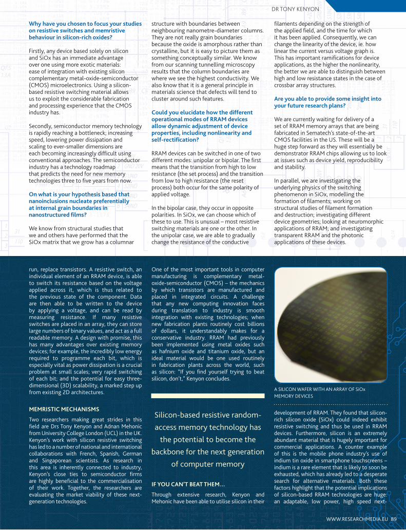
A SILICON WAFER WITH AN ARRAY OF SiOx
MEMORY DEVICES

RESISTIVE SWITCHES (RRAM) AND MEMRISTIVE BEHAVIOUR IN SILICON-RICH SILICON OXIDES
OBJECTIVES
To overcome existing memory problems using silicon oxide resistive random-access memory; a faster, lower power and higher density alternative to such technologies as flash.
TEAM MEMBERS
Dr Adnan Mehonic • Dr Wing Ng • Manveer Munde, PhD student • Luca Montesi, PhD student • Mark Buckwell, PhD student • Salman Malik, PhD student
PARTNERS
Sematech • Micron • University of Glasgow, UK • Centre national de la recherche scientifique (CNRS) Centre de Recherche sur les lons, les Matériaux et la Photonique (CIMAP), Caen, France • Universitat Autònoma de Barcelona, Spain • Forschungszetrum Jülich, Germany • Agency for Science, Technology and Research (A*STAR), Singapore
FUNDING
Engineering and Physical Sciences Research Council • UCL Business
CONTACT
Dr Tony Kenyon Reader
Department of Electronic and Electrical Engineering University College London (UCL) Torrington Place London, WC1E 7JE UK
T +44 20 7679 3270 E [email protected]
www.ee.ucl.ac.uk/~tkenyon/Photonic_Materials/Lab_home.html
DR TONY KENYON completed a DPhil in Chemical Physics at the University of Sussex in 1992 before joining the Department of Electronic and Electrical Engineering of UCL, where he currently holds the position of Reader. He is also the Department’s Postgraduate Tutor, overseeing and coordinating PhD programmes; a Fellow of the Institute of Physics; Senior Member of the IEEE; a Member of the Institution of Engineering and Technology; and serves on the Board of Delegates of the European Materials Research Society. DR ADNAN MEHONIC completed a degree in Electrical and Electronic Engineering at the University of Sarajevo, Bosnia, in 2009 and was awarded the best student in the generation prize by the University. He then undertook a Master’s in Nanotechnology at UCL, UK, in 2010, with a further award from Oxford Instruments for the best MSc project prize that year. He recently defended his PhD thesis, which was also conducted at UCL, under Kenyon’s tutelage.
ARRAYS OF RRAM DEVICES OF VARYING SIZES ON A SILICON WAFER
generation memory capability that slots directly into current fabrication processes and uses readily available materials.
The resistive switching behaviour exhibited by SiOx films led to further investigation of their electronic properties, and the use of atomic force and scanning tunnelling microscopies to understand their structure and determine a possible switching mechanism. SiOx films have large numbers of oxygen vacancies, which are locations in the crystal lattice where oxygen atoms are missing. Oxygen vacancies can hop from one position to another through the lattice and this movement can be controlled by applying a voltage. These vacancies have a tendency to drive the formation of silicon nanoinclusions, which continue to nucleate with the applied field until there are eventually enough of them to create a thin conducting filament stretching across the entire film. Importantly, the diameter of such filaments can be less than 10 nm. The resistance of the film then drops hugely and the filament remains, even when the applied voltage is removed; in essence, the film ‘remembers’ that a voltage used to exist. In 2012, Mehonic and Kenyon published this model in the Journal of Applied Physics.
A NEW ERA
As a result of this research, a potential new memory technology has moved from a developing possibility, hindered by issues around implementation, to a feasible commercial silicon system. The semiconductor industry has
been reliant on the increased downscaling of existing architectures for improved performance for many years, and as these technologies begin to reach their theoretical and practical limits it becomes ever more vital for academia to supply and develop further possibilities.
The links that Kenyon, Mehonic and colleagues are maintaining with semiconductor firms are crucial; there is a well-known struggle within academia to effectively exploit potential innovations by cultivating ties with industry. If the work carried out by these researchers continues to progress at the current rate, silicon-based RRAM technology has the potential to become the backbone for the next generation of computer memory.
90 INTERNATIONAL INNOVATION
INTELLIGENCE