the jtag interface: an attacker’s perspective · pdf file2 paper an introduction to...
TRANSCRIPT

Technical Paper
The JTAG Interface: AN ATTACKER’S PERSPECTIVE
Alain IamburgResearch ScientistOptiv

1 Optiv Technical Paper
Introduction
Embedded devices often contain powerful system interfaces that allow engineers to program flash memory, manipulate a chip’s external pin states, or take full control of a live CPU via On-Chip Debugging (OCD). These abilities are also useful for vulnerability research and exploitation. This article is intended to provide security researchers with a practical foundation for working with the JTAG interface, which is one of the most ubiquitous standards in the industry.
A Brief History of Debug Interfaces
Traditionally, in-circuit testing of embedded devices was carried out with bed-of-nails test fixtures. Spring-loaded probes would make physical contact with test pads on the PCB to communicate with chips and test for functionality or failures in different areas including:
• Circuit soldering or component assembly• Functional interaction between microcontrollers or components
Figure 1: Many Test Pads on a PCB
Figure 2: PCB Bed-of-Nails Test Fixture

2 Optiv Technical Paper
An Introduction to Joint Test Access Group (JTAG)
JTAG (IEEE 1149.1) is one of the most widely deployed test/debug standards for embedded devices. The following signals are used:
JTAG can be implemented for a single target device, or many on the same board via daisy chaining. This makes it possible to interact with many chips on a board using only a single port.
Name Description
TMS Mode Select
TCK Clock
TDI Data In
TDO Data Out
nTRST TAP/JTAG Reset (optional; may be required for your target)
nSRST System/CPU Reset (optional; may be required for your target)
VTRef Target Reference Voltage (may be required for your tools)
Figure 3: JTAG Wiring Diagram (source: Wikipedia)
As newer devices became more densely packed with complex ICs, the old testing methodology became insufficient to meet the demands of high-performance system designs. Modern debug interfaces addressed these shortcomings and were eventually equipped with more advanced system debugging functionality.

3 Optiv Technical Paper
The following Marvell board exposes a JTAG header. This board includes silkscreen markings identifying the test pads as “W_TDI”, “W_TCK”, “W_TDO”, and “W_TMS”.
The following board from a wireless router includes a JTAG header with a silkscreen label, however the header does not indicate which pads correspond to which JTAG signals.
The JTAG header below does not contain descriptive labels other than “DJ1”.
Figure 4: JTAG Test Points (1)
Figure 5: JTAG Test Points (2)
Figure 6: JTAG Test Points (3)

4 Optiv Technical Paper
Under the hood, the JTAG Test Access Port (TAP) is a 16-state finite state machine made up of the following components:
• Instruction Register (IR)› Fixed length› Used to load instructions
• Data Registers (DRs)› Variable length› Used for data I/O
• TAP Controller› Handles state machine logic› Implements core JTAG instructions› Clocks data in and out
This basic framework is leveraged and extended to provide device- or vendor-specific higher-level functionality such as:
• Reading and writing internal memory• On-chip debugging (break, step)• Indirect access to other connected on-board components such as SPI, I²C, or CFI chips via the SoC’s external
pins
The rising edge of the clock (TCK) loads input data from TMS and TDI, and executes state transitions based on the value of TMS and the current state. The falling edge of the clock sends data out of TDO.
Figure 7: Debug and Test Access Block Boundary (source: Lauterbach GmbH)
5 Optiv Technical Paper
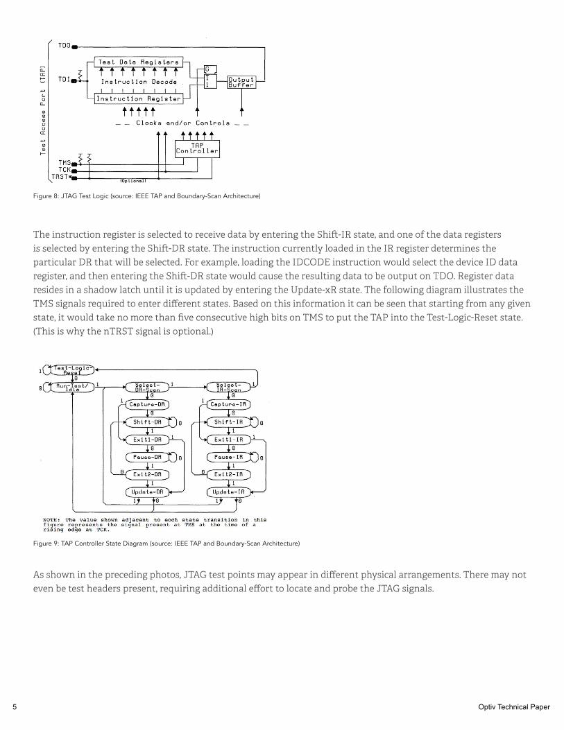
The instruction register is selected to receive data by entering the Shift-IR state, and one of the data registers is selected by entering the Shift-DR state. The instruction currently loaded in the IR register determines the particular DR that will be selected. For example, loading the IDCODE instruction would select the device ID data register, and then entering the Shift-DR state would cause the resulting data to be output on TDO. Register data resides in a shadow latch until it is updated by entering the Update-xR state. The following diagram illustrates the TMS signals required to enter different states. Based on this information it can be seen that starting from any given state, it would take no more than five consecutive high bits on TMS to put the TAP into the Test-Logic-Reset state. (This is why the nTRST signal is optional.)
As shown in the preceding photos, JTAG test points may appear in different physical arrangements. There may not even be test headers present, requiring additional effort to locate and probe the JTAG signals.
Figure 8: JTAG Test Logic (source: IEEE TAP and Boundary-Scan Architecture)
Figure 9: TAP Controller State Diagram (source: IEEE TAP and Boundary-Scan Architecture)

6 Optiv Technical Paper
Indeed, a continuity test shows the even-numbered test points of the DJ1 header are tied to ground. A JTAGulator is used to automate the enumeration of the remaining header pins.
The JTAGulator is controlled via a serial shell that is exposed over its USB interface. The tool can enumerate JTAG pins on a target device via two scan types that take advantage of the specifications in the JTAG standard. The following output shows the process of using the JTAGulator (on channels 0-5) to enumerate the odd numbered pins of the DJ1 header. First the target voltage of 3.3v is selected.
Name Pin Name
nTRST 1 2 GND
TDI 3 4 GND
TDO 5 6 GND
TMS 7 8 GND
TCK 9 10 GND
nSRST 11 12 KEY
Figure 10: JTAGulating the DJ1 Header
Reverse Engineering JTAG Connections Many standard PCB layouts exist for JTAG headers according to the target platform, which can provide a starting point for discovering actual pin to signal assignments. The Broadcom CPU from Figure 6 is MIPS-based therefore it would be reasonable to guess it uses the EJTAG standard pinout:

7 Optiv Technical Paper
$ picocom --baud 115200 /dev/tty.usbserial-A5028BXW picocom v1.7
port is : /dev/tty.usbserial-A5028BXWflowcontrol : nonebaudrate is : 115200parity is : nonedatabits are : 8escape is : C-alocal echo is : nonoinit is : nonoreset is : nonolock is : nosend_cmd is : sz -vvreceive_cmd is : rz -vvimap is : omap is : emap is : crcrlf,delbs,
Terminal ready
Welcome to JTAGulator. Press ‘H’ for available commands.
:hJTAG Commands:I Identify JTAG pinout (IDCODE Scan)B Identify JTAG pinout (BYPASS Scan)D Get Device ID(s)T Test BYPASS (TDI to TDO)
UART Commands:U Identify UART pinoutP UART passthrough
General Commands:V Set target I/O voltage (1.2V to 3.3V)R Read all channels (input)W Write all channels (output)J Display version informationH Display available commands
:jJTAGulator FW 1.3Designed by Joe Grand, Grand Idea Studio, Inc.Main: jtagulator.comSource: github.com/grandideastudio/jtagulatorSupport: www.parallax.com/support
:vCurrent target I/O voltage: UndefinedEnter new target I/O voltage (1.2 - 3.3, 0 for off): 3.3New target I/O voltage set: 3.3Ensure VADJ is NOT connected to target!
IDCODE ScanThe JTAGulator’s IDCODE scan identifies the TDO, TCK, and TMS pins by successfully reading out the device ID. A device may have an IDCODE instruction for reading out the device ID, however the JTAG standard dictates that the device ID should be loaded into the data register at reset. Therefore by resetting the TAP and then holding it in the Shift-DR state, we should receive the device ID over TDO. Note that the TDI and nTRST pins are not involved in this scan.

8 Optiv Technical Paper
The scan enumerated the following pins:
Channel DJ1 Header Pin JTAG Signal
2 5 TDO
3 7 TMS
4 9 TCK
We can observe the data traffic on the wires using a logic analyzer wired in parallel with the JTAGulator:
The scan completed in roughly 0.7 seconds. Zooming in to the last permutation in the trace, it is possible to follow the state changes and data transfers as shown in Figure 12.
Figure 11: JTAGulator IDCODE Scan (full trace)
:iEnter starting channel [0]: Enter ending channel [0]: 5Possible permutations: 120Press spacebar to begin (any other key to abort)... JTAGulating! Press any key to abort...
TDI: N/ATDO: 2TCK: 4TMS: 3TRST#: 0TRST#: 1-IDCODE scan complete.
Figure 12: JTAGulator IDCODE Scan (final, successful permutation)

9 Optiv Technical Paper
Initially the TAP is brought to the reset state and then it is placed into the Shift-DR state, at which point data is seen on TDO. State changes are indicated by a white dot in the TMS waveform. Recall that from any initial state, five high bits (“1”s) in a row will bring the TAP into the Test-Logic-Reset state. In case the logic trace is unclear, the following table illustrates the state changes:
BYPASS ScanThis scan uses the BYPASS instruction to discover the TDI pin. The BYPASS instruction causes input on TDI to be shifted through a 1-bit data register and out of TDO, skipping the chip’s internal logic. Therefore by sending a bit pattern to target pins and monitoring the previously discovered TDO pin for matching data, it is possible to discover the TDI pin. Also since the BYPASS data register is always one bit wide, this scan can determine the number of devices on the JTAG chain by counting how many bits must be shifted in before the first bit appears on TDO.
We can observe the mechanics of the scan using the Saleae logic analyzer. The trace shows the standard JTAG BYPASS instruction (all 1s) being shifted into the instruction register. Then, a random bit stream sent out on the candidate TDI pin is seen coming back out of TDO after a delay of 1 clock cycle. This scan confirms the identity of the TDI pin and the fact that there is only 1 device on the JTAG chain.
Clock Cycles
TMS 1 1 1 1 1 0 1 0 0...0 1 1 0
TAP State ? ? ? ?
Test-Logic-Reset
Run-Test/Idle Select-DR-Scan Capture-DR Shift-DR Exit1-DR Update-DR Run-Test/Idle
TDO n/a 0xF801807F n/a
:bEnter starting channel [0]: Enter ending channel [5]: Are any pins already known? [y/N]: yEnter X for any unknown pin.Enter TDI pin [0]: xEnter TDO pin [2]: Enter TCK pin [4]: Enter TMS pin [3]: Possible permutations: 6Press spacebar to begin (any other key to abort)... JTAGulating! Press any key to abort...
TDI: 1TDO: 2TCK: 4TMS: 3TRST#: 0Number of devices detected: 1
BYPASS scan complete.
10 Optiv Technical Paper
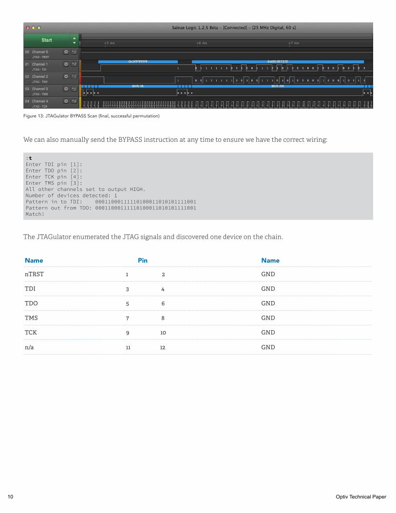
We can also manually send the BYPASS instruction at any time to ensure we have the correct wiring:
The JTAGulator enumerated the JTAG signals and discovered one device on the chain.
Figure 13: JTAGulator BYPASS Scan (final, successful permutation)
Name Pin Name
nTRST 1 2 GND
TDI 3 4 GND
TDO 5 6 GND
TMS 7 8 GND
TCK 9 10 GND
n/a 11 12 GND
:tEnter TDI pin [1]: Enter TDO pin [2]: Enter TCK pin [4]: Enter TMS pin [3]: All other channels set to output HIGH.Number of devices detected: 1Pattern in to TDI: 00011000111110100011010101111001Pattern out from TDO: 00011000111110100011010101111001Match!

11 Optiv Technical Paper
Instruction Data Register Function
BYPASS BYPASS Register (1-bit long) Connects TDI and TDO via the BYPASS register
EXTEST Boundary Scan Register (BSR)
Connects TDI and TDO via the BSRReads/toggles device external pin states• Pin states are captured in the Capture-DR state• New values are shifted into the BSR in the Shift-DR state• New values are applied to device pins in the Update-DR state
SAMPLE / PRELOAD
Boundary Scan Register (BSR)
Connects TDI and TDO via the BSR
Device is left in normal functioning mode (i.e. read-only)
BSR is scanned to take a sample of device pin states
Also used to preload test data into the BSR prior to executing EXTEST
IDCODE ID RegisterConnects TDI and TDO via the IDCODE register
Returns vendor/device ID
INTEST Boundary Scan Register (BSR)
Connects TDI and TDO via the BSR
Like EXTEST, but used for the manipulation of on-chip internal logic (e.g. in a CPLD) instead of external pins
I highly recommend watching EEVblog #499 for a beautiful explanation of JTAG and boundary scan from an engineer’s perspective.
Figure 14: Core JTAG Functionality (Source: XJTAG)
System Access via JTAG (Low Level) The following are common JTAG instructions and their corresponding data registers. The first three must be implemented in a device for it to be considered IEEE 1149.1 compliant, and the last two are optional.
12 Optiv Technical Paper
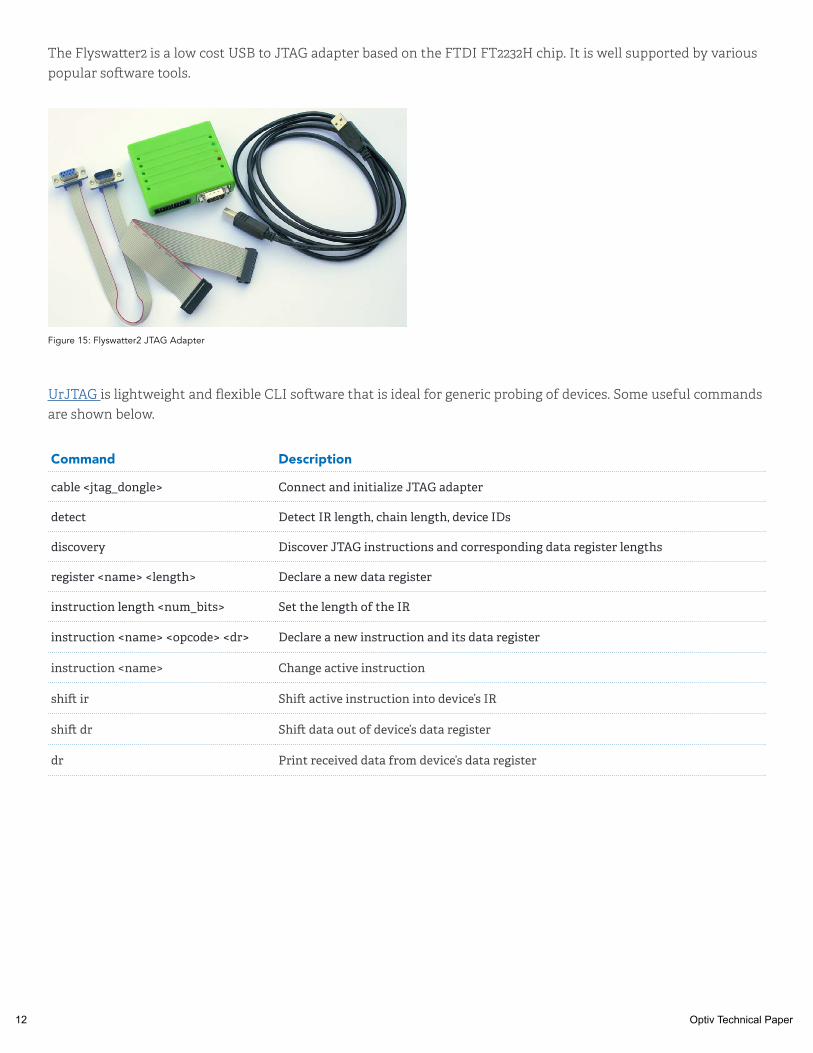
The Flyswatter2 is a low cost USB to JTAG adapter based on the FTDI FT2232H chip. It is well supported by various popular software tools.
UrJTAG is lightweight and flexible CLI software that is ideal for generic probing of devices. Some useful commands are shown below.
Figure 15: Flyswatter2 JTAG Adapter
Command Description
cable <jtag_dongle> Connect and initialize JTAG adapter
detect Detect IR length, chain length, device IDs
discovery Discover JTAG instructions and corresponding data register lengths
register <name> <length> Declare a new data register
instruction length <num_bits> Set the length of the IR
instruction <name> <opcode> <dr> Declare a new instruction and its data register
instruction <name> Change active instruction
shift ir Shift active instruction into device’s IR
shift dr Shift data out of device’s data register
dr Print received data from device’s data register

13 Optiv Technical Paper
The target Broadcom device was detected with an instruction register length of 32. UrJTAG didn’t recognize the particular device ID, but it discovered some potential JTAG instructions by brute forcing the instruction register and measuring the length of the corresponding data register.
UrJTAG lets you manually send commands over a JTAG chain. This may be used to invoke standard and/or undocumented functionality on devices. The following information is required to prepare a JTAG instruction via UrJTAG:
• Instruction register length
• Data register name and length
• Instruction name, opcode and associated data register
To execute an instruction, it is shifted into the instruction register. Then, the data register is shifted out to read the result. UrJTAG handles the required state changes behind the scenes. The ‘dr’ command simply prints the last contents that were shifted out of the data register. Arbitrary names can be chosen for instructions and registers, but I am naming these based on knowledge of their purpose.
The ‘0x6’ instruction turned out to be IDCODE. The ‘0x8’ instruction below is more interesting. It has a long data register of 116 bits, which is likely the BSR containing the pin states of the BGA SoC, and this instruction is likely SAMPLE or EXTEST. Shifting the data register, the states of the chip’s pins are returned.
UrJTAG 0.10 #2007Copyright (C) 2002, 2003 ETC s.r.o.Copyright (C) 2007, 2008, 2009 Kolja Waschk and the respective authors
UrJTAG is free software, covered by the GNU General Public License, and you arewelcome to change it and/or distribute copies of it under certain conditions.There is absolutely no warranty for UrJTAG.
warning: UrJTAG may damage your hardware!Type “quit” to exit, “help” for help.
jtag> cable flyswatterConnected to libftdi driver.jtag> detectIR length: 32Chain length: 1Device Id: 00010000000111001010000101111111 (0x101CA17F) Manufacturer: Broadcom (0x17F) Unknown part! (0000000111001010) (/usr/share/urjtag/broadcom/PARTS)jtag> discoveryDetecting IR length ... 32Detecting DR length for IR 11111111111111111111111111111111 ... 1Detecting DR length for IR 00000000000000000000000000000000 ... 1Detecting DR length for IR 00000000000000000000000000000001 ... warning: TDO seems to be stuck at 0Detecting DR length for IR 00000000000000000000000000000010 ... warning: TDO seems to be stuck at 0Detecting DR length for IR 00000000000000000000000000000011 ... warning: TDO seems to be stuck at 0Detecting DR length for IR 00000000000000000000000000000100 ... warning: TDO seems to be stuck at 0Detecting DR length for IR 00000000000000000000000000000101 ... 37Detecting DR length for IR 00000000000000000000000000000110 ... 32Detecting DR length for IR 00000000000000000000000000000111 ... 1Detecting DR length for IR 00000000000000000000000000001000 ... 116
jtag> instruction length 32jtag> register ID 32jtag> instruction IDCODE 00000000000000000000000000000110 IDjtag> instruction IDCODEjtag> shift irjtag> shift drjtag> dr00010000000111001010000101111111 (0x101CA17F)

14 Optiv Technical Paper
When running this instruction again with the WPS button held down, the same data is returned but with one bit cleared. Notice the data marked in red. This bit represents the SoC’s external I/O pin that is connected to the button.
Figure 16: WPS Button
This shows how to monitor SoC pin states at a low level over JTAG. New pin states could be toggled by shifting data into the DR via “dr <data>.” I am only touching on some functionality of UrJTAG.
Another tool, TopJTAG Probe, is useful for visualizing boundary scan operations while reading or toggling individual pins. The only required input is a Boundary Scan Description Language (BSDL) file, which identifies a SoC’s pin mappings and JTAG instructions/registers. Some sources for BSDL files are here, here, and here.
Figure 17: TopJTAG Probe Boundary Scan Software
jtag> register BSR 116jtag> instruction SAMPLE 00000000000000000000000000001000 BSRjtag> instruction SAMPLEjtag> shift irjtag> shift drjtag> dr00000100000101000000000000000000000101010001010100010001000000000000000000000000000101010101010100010100000000010001 (0x00000000000001000000155514011)
jtag> print instructions Active Instruction Register -------------------------------------------------------------- X SAMPLE BSR IDCODE ID jtag> shift drjtag> dr00000100000101000000000000000000000101010001010100010001000000000000000000000000000101010101010100010000000000010001 (0x00000000000001000000155510011)

15 Optiv Technical Paper
System Access via JTAG (Medium Level)The ability to read and toggle a chip’s external pins is intriguing because it means we can communicate with other connected chips on the board. The following diagram illustrates the data flow (in this case, depicting a parallel flash chip).
Figure 18: Accessing External Flash via JTAG Boundary Scan (Source: Intellitech.com)
Various software tools exist for dumping external flash via boundary scan, such as UrJTAG, J-Flash, and TopJTAG Flash Programmer. The USB JTAG NT adapter supports boundary scan and some vendor extensions via its accompanying software as shown below.
Figure 19: USB JTAG NT Adapter
USBJTAG NT detected and dumped an external W25Q64CV serial flash chip via the EXTEST instruction.
Copyright (C) 2010-2015USB JTAG NT 0.71aTarget: E800-detectIDCODE 1008C17FBroadcom BCM008CIMPCODE 60414000EJTAG V2.6DMA not supportedFound Address= 00000000 W25Q64CV-getram 0 800000Time 00:08:30 (.697)

16 Optiv Technical Paper
Figure 20: SPI Flash Dumped via JTAG Boundary Scan
This was done by shifting bits through the JTAG chain and directly interfacing with the pins of the attached SPI chip.

17 Optiv Technical Paper
Figure 21: JTAG Debug/Programming Logic (Source: XJTAG)
Instruction Function
IMPCODE Selects the implementation register
ADDRESS Selects the address register
DATA Selects the data register
CONTROL Selects the EJTAG control register
EJTAGBOOT Selects the bypass register and sets EjtagBrk, ProbEn and ProbTrap to 1 as reset value
TCBCONTROLA Selects the TCBTCONTROLA register in the trace control block
TCBDATA Selects the TCBDATA register in the trace control block
For example the following are a subset of instructions defined by EJTAG, which is a MIPS extension of JTAG:
The SEGGER J-Link adapter is suitable for professional engineering work and has native support for many target chips such as the ARM-based Marvell device in Figure 4.
System Access via JTAG (High Level)As previously shown, the JTAG interface defines low-level data I/O and basic logic. In order to implement functionality such as on-chip debugging, it is necessary to invoke vendor-specific instructions, data registers, and initialization sequences.

18 Optiv Technical Paper
Figure 22: J-Link JTAG Adapter
The J-Flash software includes vendor-specific JTAG initialization sequences for a large number of target chips including virtually every ARM device, allowing access to internal memory.
OpenOCD is a tool that is geared towards embedded system debugging and programming. Ideally, once the bridge is established it is possible to obtain low-level control of the target CPU in much the same way a local debugger controls the CPU on a PC. OpenOCD includes support for various JTAG adapters and CPU targets via configuration files. We will use a Linksys WRT54GL as a target device.
The relevant inputs are:
• Adapter Configuration (jlink.cfg)› Defines and configures the link driver for talking with the JTAG adapter
• Board Configuration (linksys-wrt54gl.cfg)› Defines attached CFI flash and memory mapping
• Target Configuration (bcm5352e.cfg)› Defines CPU ID and IR length› Defines the architecture and bus driver
Figure 23: Dumping Internal Flash via JTAG

19 Optiv Technical Paper
OpenOCD serves a CLI control service on port 4444.
$ cat interface/jlink.cfg ## Segger J-Link## http://www.segger.com/jlink.html#
interface jlinktransport select jtagadapter_khz 6000
$ cat board/linksys-wrt54gl.cfg ## Linksys WRT54GL v1.1#
source [find target/bcm5352e.cfg]
set partition_list { CFE { Bootloader 0x1c000000 0x00040000 } firmware { “Kernel+rootfs” 0x1c040000 0x003b0000 } nvram { “Config space” 0x1c3f0000 0x00010000 }}
# External 4MB NOR Flash (Intel TE28F320C3BD90 or similar)set _FLASHNAME $_CHIPNAME.flashflash bank $_FLASHNAME cfi 0x1c000000 0x00400000 2 2 $_TARGETNAME
$ cat target/bcm5352e.cfgset _CHIPNAME bcm5352eset _CPUID 0x0535217f
jtag newtap $_CHIPNAME cpu -irlen 8 -expected-id $_CPUID
set _TARGETNAME $_CHIPNAME.cputarget create $_TARGETNAME mips_m4k -endian little -chain-position $_TARGETNAME
gdb_memory_map disable
$_TARGETNAME configure -event gdb-attach { reset halt }
$ sudo openocd -f interface/jlink.cfg -f board/linksys-wrt54gl.cfg Open On-Chip Debugger 0.10.0-dev-00212-g50d4f76-dirty (2016-08-22-13:29)Licensed under GNU GPL v2For bug reports, read http://openocd.org/doc/doxygen/bugs.htmladapter speed: 6000 kHzInfo : No device selected, using first device.Info : J-Link ARM V8 compiled Sep 22 2014 23:26:43Info : Hardware version: 8.00Info : VTarget = 3.351 VInfo : clock speed 6000 kHz

20 Optiv Technical Paper
In addition OpenOCD starts up a GDB server on port 3333, providing a familiar debugging environment of the live device.
$ telnet localhost 4444Trying 127.0.0.1...Connected to localhost.Escape character is ‘^]’.Open On-Chip Debugger> scan_chain TapName Enabled IdCode Expected IrLen IrCap IrMask-- ------------------- -------- ---------- ---------- ----- ----- ------ 0 bcm5352e.cpu Y 0x0535217f 0x0535217f 8 0x01 0x03> targets TargetName Type Endian TapName State -- ------------------ ---------- ------ ------------------ ------------ 0* bcm5352e.cpu mips_m4k little bcm5352e.cpu running> haltbcm5352e.cpu: target state: haltedtarget halted in MIPS32 mode due to debug-request, pc: 0x80003260> targets TargetName Type Endian TapName State -- ------------------ ---------- ------ ------------------ ------------ 0* bcm5352e.cpu mips_m4k little bcm5352e.cpu halted>
gdb$ set architecture mipsThe target architecture is assumed to be mipsgdb$ target remote localhost:3333Remote debugging using localhost:3333gdb$ i r zero at v0 v1 a0 a1 a2 a3 R0 00000000 00000000 01000000 00000001 9fc2b590 8032b590 00010a40 00000001 t0 t1 t2 t3 t4 t5 t6 t7 R8 0c0cabce 1fc00000 aa55beef 00000000 00000008 00000200 9fc02278 9fc037f4 s0 s1 s2 s3 s4 s5 s6 s7 R16 00000002 1c266e56 000001c6 803a3312 00000002 a0000000 803a3138 00000000 t8 t9 k0 k1 gp sp s8 ra R24 ffffffff 9fc03b10 00004000 9fc02f9c 00000000 803a3128 bfc02180 1f900000 status lo hi badvaddr cause pc 00400000 00002000 00000000 00000000 00000000 9fc02334 fcsr fir 00000000 00000000 gdb$ x/20i $pc=> 0x9fc02334: sw t0,0(a1) 0x9fc02338: addi a0,a0,4 0x9fc0233c: addi a1,a1,4 0x9fc02340: addi a2,a2,-4 0x9fc02344: bnez a2,0x9fc02330 0x9fc02348: nop 0x9fc0234c: nop 0x9fc02350: lui a0,0x5a42 0x9fc02354: ori a0,a0,0x5353 0x9fc02358: bal 0x9fc02360 0x9fc0235c: nop 0x9fc02360: nop 0x9fc02364: lui k1,0x8030 0x9fc02368: addiu k1,k1,9056 0x9fc0236c: subu ra,ra,k1 0x9fc02370: lui k1,0x8030 0x9fc02374: addiu k1,k1,8232 0x9fc02378: addu k1,k1,ra 0x9fc0237c: lw k1,4(k1) 0x9fc02380: bal 0x9fc02388 0x9fc02384: nopgdb$ x/20x $sp+0x500x803a3178: 0x803276e4 0xffffffff 0x00000001 0xffffffff0x803a3188: 0x00000000 0x00000000 0x00000000 0xffffffff0x803a3198: 0x00000007 0xffffffff 0x8033f0a8 0xffffffff0x803a31a8: 0x00000fe0 0xffffffff 0x803a3200 0x000000000x803a31b8: 0x80327948 0x80327914 0x803a3289 0x00000000
21 Optiv Technical Paper
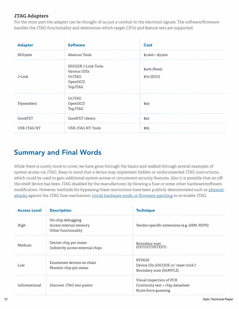
JTAG AdaptersFor the most part the adapter can be thought of as just a conduit to the electrical signals. The software/firmware handles the JTAG functionality and determines which target CPUs and feature sets are supported.
Adapter Software Cost
BDI3000 Abatron Tools $1,000—$3,000
J-Link
SEGGER J-Link ToolsVarious IDEsUrJTAGOpenOCDTopJTAG
$400 (Base)
$70 (EDU)
Flyswatter2UrJTAGOpenOCDTopJTAG
$90
GoodFET GoodFET clients $50
USB JTAG NT USB JTAG NT Tools $65
Summary and Final Words
While there is surely more to cover, we have gone through the basics and walked through several examples of system access via JTAG. Keep in mind that a device may implement hidden or undocumented JTAG instructions, which could be used to gain additional system access or circumvent security features. Also it is possible that an off-the-shelf device has been JTAG disabled by the manufacturer, by blowing a fuse or some other hardware/software modification. However, methods for bypassing these restrictions have been publicly demonstrated such as physical attacks against the JTAG fuse mechanism, trivial hardware mods, or firmware patching to re-enable JTAG.
Access Level Description Technique
HighOn-chip debuggingAccess internal memoryOther functionality
Vendor-specific extensions (e.g. ARM, MIPS)
MediumGet/set chip pin statesIndirectly access external chips
Boundary scan (EXTEST/INTEST)
LowEnumerate devices on chainMonitor chip pin states
BYPASSDevice IDs (IDCODE or “reset trick”)Boundary scan (SAMPLE)
Informational Discover JTAG test pointsVisual inspection of PCBContinuity test + chip datasheetBrute force guessing

22 Optiv Technical Paper
Looking forward, efforts are underway to implement modern features on top of JTAG such as the IEEE 1500 and IEEE 1687 standards. These are briefly compared below.
Hopefully you have expanded your working knowledge of JTAG and can apply these techniques in your research.
Figure 24: JTAG vs IJTAG vs ECT (Source: asset-intertech.com)
Figure 25: JTAG vs. IJTAG (Source: ElectronicDesign.com)

Optiv is the largest holistic pure-play cyber security solutions provider in North Ameri-ca. The company’s diverse and talented employees are committed to helping businesses, governments and educational institutions plan, build and run successful security programs through the right combination of products, services and solutions related to security program strategy, enterprise risk and consulting, threat and vulnerability management, enterprise incident management, security architecture and implemen-tation, training, identity and access management, and managed security. Created in 2015 as a result of the Accuvant and FishNet Security merger, Optiv is a Blackstone (NYSE: BX) portfolio company that has served more than 12,000 clients of various sizes across multiple industries, offers an extensive geographic footprint, and has premium partnerships with more than 300 of the leading security product manufacturers. For more information, please visit www.optiv.com.© 2016 Optiv Security Inc. All Rights Reserved.
11.16 | F1
References
EEE Std 1149.1-2001 Test Access Port and Boundary-Scan Architecture, IEEE, http://fiona.dmcs.pl/~cmaj/JTAG/JTAG_IEEE-Std-1149.1-2001.pdf
The Test Access Port and Boundary-Scan Architecture, C. Maunder and R. Tulloss, http://fiona.dmcs.pl/~cmaj/JTAG/Test Access Port And Boundary Scan Architecture - C. Maunder R. Tulloss.pdf
IEEE Std 1149.1 (JTAG) Testability Primer, Texas Instruments, http://www.ti.com/lit/an/ssya002c/ssya002c.pdf
JTAG Interface Training, Lauterbach GmbH, http://www.lauterbach.com/pdf/training_jtag.pdf
Blackbox JTAG Reverse Engineering, CCC 2009, https://events.ccc.de/congress/2009/Fahrplan/attachments/1435_JTAG.pdf
Debugging Embedded Systems with JTAG, Tactical Network Solutions, http://www.devttys0.com/wp-content/uploads/2014/04/JTAG_Slides.pdf
Assisted Discovery of On-Chip Debug Interfaces, Grand Idea Studio, Inc., http://www.grandideastudio.com/wp-content/uploads/jtagulator_slides.pdf
Technical Guide to JTAG, XJTAG, https://www.xjtag.com/about-jtag/jtag-a-technical-overview/
What is JTAG and Boundary Scan?, EEVblog #499, https://www.youtube.com/watch?v=TlWlLeC5BUs
Boundary Scan Coach, Goepel Electronic, http://www.goepel.com/en/jtag-boundary-scan/education/boundary-scan-coach.html
JTAG, EXTEST, and Hair Loss, Big Mess O’ Wires, http://www.bigmessowires.com/2011/06/26/jtag-extest-and-hair-loss/
What’s The Difference Between JTAG (IEEE 1149.1) And IJTAG (IEEE P1687)?, Martin Keim, Electronic Design, http://electronicdesign.com/boards/what-s-difference-between-jtag-ieee-11491-and-ijtag-ieee-p1687
EJTAG Specification, MIPS Technologies, http://downloads.buffalo.nas-central.org/LS2_MIPSel/DevelopmentTools/JTAG/MD00047-2B-EJTAG-SPC-03.10.pdf
EJTAG, Linux-MIPS, https://www.linux-mips.org/wiki/JTAG
MIPS32 M4K Processor Core Software User’s Manual, MIPS Technologies, https://imagination-technologies-cloudfront-assets.s3.amazonaws.com/documentation/MD00249-2B-M4K-SUM-02.03.pdf
JTAG, OpenWrt, https://wiki.openwrt.org/doc/hardware/port.jtag
JTAG, DD-WRT, http://www.dd-wrt.com/wiki/index.php/JTAG
JTAG Pinouts, JTAG Test, http://www.jtagtest.com/pinouts/
JTAG Interface Connectors, EmuTec, http://www.emutec.com/jtag_cable_interface_connector_pinout_debugjet.php
1125 17th Street, Suite 1700Denver, CO 80202800.574.0896www.optiv.com