the influence of insulator properties on the electro-optical performance of flexible zns:erf3...
TRANSCRIPT
006) 2342–2346www.elsevier.com/locate/tsf
Thin Solid Films 515 (2
The influence of insulator properties on the electro-optical performance offlexible ZnS:ErF3 alternating current thin film electroluminescent devices
Nigel Shepherd a,⁎, David C. Morton b, Eric W. Forsythe b, Dave Chiu b
a Department of Materials Science and Engineering E118, North Texas Research Park, University of North Texas Denton, TX 76203-5310, USAb U.S. Army Research Laboratory, 2800 powder Mill Road, Adelphi, MD 20783, USA
Received 7 September 2005; received in revised form 14 March 2006; accepted 5 April 2006Available online 5 June 2006
Abstract
We have developed flexible ZnS:ErF3 alternating current thin film electroluminescent devices on molybdenum foils, and quantified the effectof insulator properties for the case of alumina (Al2O3) and barium tantalate (BaTa2O6) on the device electrical characteristics, and infraredemission. The inverted, full-stack structures could be flexed in tension and compression without mechanical failure or deterioration of opticaloutput, and flex radii of a few centimeters are routinely achieved. Thus, the feasibility of a flexible, inorganic, large area electroluminescent emitterhas been demonstrated. Compared to the Al2O3 devices, the numbers for structures employing BaTa2O6 represent a 29% increase in flux density at980 nm, a 36% increase at 1540 nm, an 18% increase in conduction charge, a 10% increase in phosphor field and a 14% increase in thresholdvoltage. Our interpretation of the data is as follows: in the case of BaTa2O6, the interface states from which electrons are sourced into the phosphorare deeper, requiring a higher voltage for field emission. As a consequence, electrons are injected into the phosphor when the phosphor field ishigher, resulting in better excitation efficiency and improved optical generation. The increase in conduction charge is interpreted as a higherdensity of interface states, which appear to have a narrower energy distribution based on the more abrupt threshold behavior observed.© 2006 Elsevier B.V. All rights reserved.
Keywords: Flexible substrate; Electroluminescent devices; Inorganic; Infrared emission; Zinc suflexible
1. Introduction
The permeation of the information age into every aspect ofsociety and the continued growth of wireless communicationshave lead to projections that wearable displays are the futureanalog of a wrist-watch. High information content displays aremultifunctional and among the most effective modes of com-munication. However, wearable displays must be lightweight andflexible. As a result, flexible electronic and optoelectronic devicesare generating heightened interest. Drive amplifiers [1], electro-optic modulators [2], optoelectronic interconnects [3], thin-filmtransistors [4], infrared detectors [5] and emissive displays [6,7] onflexible substrates have all been reported.With regards to the latter,the emphasis has been on organic light emitting diodes operatingin the visible spectral region. However, for flexible display appli-cations where both visible and infrared emission are required [8],lanthanide doped inorganic thin film devices on flexible substrates
⁎ Corresponding author. Tel.: +1 940 369 7714; fax: +1 940 565 4824.E-mail address: [email protected] (N. Shepherd).
0040-6090/$ - see front matter © 2006 Elsevier B.V. All rights reserved.doi:10.1016/j.tsf.2006.04.032
are better suited because of the multiple visible and infraredradiative transitions that some lanthanide ions exhibit. Here, wereport flexible, inorganic alternating current thin film electrolu-minescent devices (ACTFELDs) with visible and infraredemission. Such devices are also potentially attractive in novelapplications such as phototherapy bandages. The clinical applica-tions of low dosage 500 nm to 2000 nm phototherapy for painrelief and the healing ofwounds, deep bruises, acute tendonitis andmusculoskeletal conditions have been described [9–11].
The physics, processing and properties of ACTFELDs havebeen reviewed in detail [12,13]. Due to the brittle nature of theinorganic ACTFELD materials, a primary consideration forflexibility is that the total device thickness must be less than thecritical thickness for cracking, delamination and general struc-tural failure, yet the constituent layers must be sufficiently thickin order to provide operational functionality. Careful attentionmust be exercised during device fabrication in order to min-imize processing induced stresses. With the natural objective ofmaximizing excitation efficiency and optical output throughmaximal charge injection, high-field transport and impact
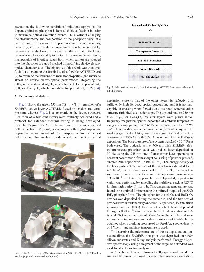
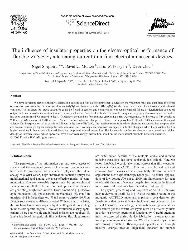
Fig. 2. Schematic of inverted, double-insulating ACTFELD structure fabricatedfor this study.
2343N. Shepherd et al. / Thin Solid Films 515 (2006) 2342–2346
excitation, the following conditions/limitations apply: (a) thedopant optimized phosphor is kept as thick as feasible in orderto maximize optical excitation events. Thus, without changingthe stoichiometry and composition of the phosphor, very littlecan be done to increase its capacitance and carrier sourcingcapability; (b) the insulator capacitance can be increased bydecreasing its thickness. However, as the insulator thicknessdecreases so does its ability to protect from over-voltage. Hence,manipulation of interface states from which carriers are sourcedinto the phosphor is a good method of modifying device electro-optical characteristics. The objective of this work was then two-fold: (1) to examine the feasibility of a flexible ACTFELD and(2) to examine the influence of insulator properties (and interfacestates) on device electro-optical performance. Regarding thelatter, we investigated Al2O3, which has a dielectric permittivityof 8, and BaTa2O6, which has a dielectric permittivity of 22 [14].
2. Experimental details
Fig. 1 shows the green 550 nm (4S3/2→4I15/2) emission of a
ZnS:ErF3 active layer ACTFELD flexed in tension and com-pression, whereas Fig. 2 is a schematic of the device structure.Flex radii of a few centimeters were routinely achieved and aprotocol for extended flexural testing is being developed.Flexible, 25 μm thick Mo foils were used as the substrate andbottom electrode. Mo easily accommodates the high-temperaturedopant activation anneal of the phosphor without structuraldeformation, it has an elastic modulus and coefficient of thermal
Fig. 1. The 4S3/2→4I15/2 (550 nm) emission of a ZnS:ErF3 ACTFELD flexed in
tension (top) and compression (bottom).
expansion close to that of the other layers, its reflectivity issufficiently high for good optical outcoupling, and it is not sus-ceptible to creasing when flexed due to its body-centered-cubicstructure (inhibited dislocation slip). The top and bottom 250 nmthick Al2O3 or BaTa2O6 insulator layers were planar radio-frequency magnetron sputter deposited at ambient temperatureusing a working pressure of 2.66 Pa and a power density of 7 W/cm2. These conditions resulted in adherent, stress-free layers. Theworking gas for the Al2O3 layers was argon (Ar) and a mixtureconsisting of 23% O2 with 77% Ar was used for the BaTa2O6
deposition. The base pressure of the systemwas 2.66×10⁻⁴ Pa inboth cases. The optically active, 700 nm thick ZnS:ErF3 elec-troluminescent phosphor layer was pulsed laser deposited at30 Hz using the 248 nm line of an excimer laser operating inconstant power mode, from a target consisting of powder-pressed,sintered ZnS doped with 1.5 mol% ErF3. The energy density ofthe laser pulses at the surface of the target was estimated to be4.7 J/cm2, the substrate was heated to 185 °C, the target tosubstrate distance was ∼ 7 cm and the deposition pressure was1.33×10−3 Pa. After the phosphor was deposited, dopant acti-vation was performed by annealing the multilayer stack at 425 °Cin ultra-high purity N2 for 1 h. This annealing temperature wasfound to be optimal for increasing the infrared output of the ZnS:ErF3 phosphor films. The phosphor for the Al2O3 and BaTa2O6
devices was deposited during the same run, and the two sets ofdevices were simultaneously annealed. A sputtered, 150 nm thickindium-tin-oxide (ITO) transparent contact layer depositedthrough a 0.28 cm2 window completed the device structure. Atypical ITO transmissivity of 85–90% in the visible and nearinfrared spectral regions, and a sheet resistance of 40–60Ω/□ isobtainedwhen aworking pressure of 0.4 Pa ofAr, a power densityof 1 W/cm2 and ambient temperature is used.
To determine the microstructure of the as-deposited and an-nealed films, the ZnS:ErF3 phosphor was deposited on ⟨100⟩silicon substrates and X-ray analysis performed. Energy disper-sive spectroscopy using a fragment of the target as a standard wasused for stoichiometric analysis.
A 2.5 kHz a.c. drivewaveformwith 30μs pulsewidths and 5μsrise and fall times was used for electroluminescence excitation.
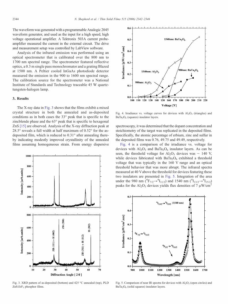
Fig. 4. Irradiance vs. voltage curves for devices with Al2O3 (triangles) andBaTa2O6 (squares) insulator layers.
2344 N. Shepherd et al. / Thin Solid Films 515 (2006) 2342–2346
Thewaveformwas generatedwith a programmableAnalogic 2045waveform generator, and used as the input for a high speed, highvoltage operational amplifier. A Tektronix 503A current probe-amplifier measured the current in the external circuit. The driveand measurement setup was controlled by LabView software.
Analysis of the infrared emission was performed using anoptical spectrometer that is calibrated over the 800 nm to1700 nm spectral range. The spectrometer featured reflectiveoptics, a 0.3 m single pass monochromator and a grating Blazedat 1500 nm. A Peltier cooled InGaAs photodiode detectormeasured the emission in the 900 to 1600 nm spectral range.The calibration source for the spectrometer was a NationalInstitute of Standards and Technology traceable 45 W quartz-tungsten-halogen lamp.
3. Results
The X-ray data in Fig. 3 shows that the films exhibit a mixedcrystal structure in both the annealed and as-depositedconditions as in both cases the 33° peak that is specific to thezincblende phase and the 63° peak that is specific to hexagonalZnS [15] are observed. Analysis of the X-ray diffraction peak at28.5° reveals a full width at half maximum of 0.52° for the as-deposited film, which is reduced to 0.31° after annealing there-by indicating modestly improved crystallinity of the annealedfilms assuming homogeneous strain. From energy dispersive
Fig. 3. XRD pattern of as-deposited (bottom) and 425 °C annealed (top), PLDZnS:ErF3 phosphor films.
spectroscopy, it was determined that the dopant concentration andstoichiometry of the target was replicated in the deposited films.Specifically, the atomic percentage of erbium, zinc and sulfur inthe deposited films was 0.76, 49.75 and 49.49, respectively.
Fig. 4 is a comparison of the irradiance vs. voltage fordevices with Al2O3 and BaTa2O6 insulator layers. As can beseen, the threshold voltage for Al2O3 devices was ∼ 140 V,while devices fabricated with BaTa2O6 exhibited a thresholdvoltage that was typically in the 160 V range and an opticalthreshold behavior that was more abrupt. The infrared spectrameasured at 40 Vabove the threshold for devices featuring thesetwo insulators are presented in Fig. 5. Integration of the areaunder the 980 nm (4F7/2→
4I11/2) and 1540 nm (4I13/2→4I15/2)
peaks for the Al2O3 devices yields flux densities of 7 μW/cm2
Fig. 5. Comparison of near IR spectra for devices with Al2O3 (open circles) andBaTa2O6 (solid squares) insulator layers.

Fig. 6. Comparison of conduction charge vs. phosphor field for devices withAl2O3 (squares) and BaTa2O6 (stars) insulator layers.
2345N. Shepherd et al. / Thin Solid Films 515 (2006) 2342–2346
and 22 μW/cm2, respectively. For BaTa2O6 devices, the 980 nmflux density was 9 μW/cm2 and, at 1540 nm, it was 30 μW/cm2.Compared to the Al2O3 devices, the numbers for structuresemploying BaTa2O6 represent a 29% increase in flux density at980 nm, a 36% increase at 1540 nm. It should be noted that theirradiance values reported herein have not been corrected forspatial distribution, i.e., the collection angle of the mirror(70.2°) used to collect the emitted light.1 When this correction isconsidered, the values given above must be increased by afactor of 2.56 (π°/70.2) yielding 17.9 μW/cm2 at 980 nm and59 μW/cm2 at 1550 nm for Al2O3. The corresponding values forBaTa2O6 are 23 μW/cm2 at 980 nm and 77 μW/cm2 at 1550 nm.
To better understand the observed dependences of opticaloutput and threshold behaviors on insulator material, electricalcharacterization was performed using the standard methodology[16,17]. That is, the external charge (Qext) was determined fromtime integration of the external current and the total capacitance(Ct) of the device was determined from the slope of the ‘pre-threshold’ Qext vs. V plot. The insulator capacitance (Ci) wasdetermined from the slope of the Qext vs. V plot in the regionimmediately following the threshold voltage. Having measuredthe total device and insulator capacitances, the phosphorcapacitance was calculated (Cp=CiCt/Ci−Ct). The conductioncharge was then derived according to [16]:
Qint ¼ Ci þ Cp
CiQext−Cp Vap
� �and the phosphor field according to :
Fp ¼ 1tp
Qext
Ci−Vap
� �:
1 Because of the use of screens and apertures during the calibrationprocedure, a directional beam of light is produced, which is completelycollected and focused into the monochromator. The emission from ACTFELDsis diffuse.
In the above equations, Qint is the conduction or transferredcharge, Vap is the applied voltage, Fp is the phosphor field and tpis the phosphor thickness. The obtained transferred chargeversus phosphor field plots are shown in Fig. 6. The phosphorfield and conduction charge at 40 V above threshold are2.1 MV/cm and 5 μC/cm2 for the Al2O3 devices. The cor-responding numbers for BaTa2O6 devices are 2.3 MV/cm and6 μC/cm2, respectively. These numbers represent an 18% in-crease in conduction charge, a 10% increase in phosphor fieldand a 14% increase in threshold voltage for the BaTa2O6 de-vices compared to those with Al2O3.
4. Discussion
Considering that phosphor thickness, deposition and annealwas essentially identical for both sets of devices, it is unlikelythat bulk trapping in the phosphor is a significant contributor tothe observed differences. The optical and electrical data in-dicates that in the case of BaTa2O6, the interface states fromwhich electrons are injected into the phosphor are deeperrequiring a higher voltage for field emission, and are higher indensity as evidenced by the increase in conduction charge. As aconsequence, electrons are injected into the phosphor when thephosphor field is higher, which couples with a larger numberinjected to result in better excitation efficiency and improvedoptical generation. The interface states appear to have a nar-rower energy distribution based on the more abrupt thresholdbehavior observed. In summary, we have demonstrated thefeasibility of a flexible ACTFELD, and how the possible loss ofoptical output associated with the tradeoff between phosphorthickness and device flexibility can be at least partially com-pensated for by judicious choice of the insulator material, as thisquantitative optical and electrical analysis shows for Al2O3 andBaTa2O6.
Acknowledgements
We thank Dr. Jay Molstad of Maxion Technologies forassisting with the EDS analysis. This work was supported by theU.S. Army Research Laboratory Postdoctoral Fellowship Pro-gram (administered by Oak Ridge Associated Universities).
References
[1] R.J. Filkins, J. Iannotti, G. Claydon, K. Durocher, C. Kapusta, S.Dasgupta, M. Nielsen, in: K. Dutta, A.A.S. Awwal, N.K. Dutta, K. Fujiura(Eds.), Active and passive optical components for WDM communications,August 2003, SPIE Proc., vol. 5246, 2003, p. 250.
[2] H.-C. Song, M.-C. Oh, S.-W. Ahn, H. Steier, H.R. Fetterman, C. Zhang,Appl. Phys. Lett. 82 (2003) 4432.
[3] L.A. Eldada, in: M.R. Feldman, R.L. Li, W.B. Matkin, S. Tang (Eds.),Optoelectronic interconnects: VII. Photonics packaging and integration II,April 2000, SPIE Proc., vol. 3952, 2000, p. 190.
[4] C. Gray, J. Wang, G. Duthaler, A. Ritenour, P.S. Drzaic, in: D. Fichou, Z.Bao (Eds.), Organic field effect transistors, December 2001, SPIE Proc.,vol. 4466, 2001, p. 89.
[5] Z. Celik-Butler, D.P. Butler, A. Yildiz, in: E.L. Dereniak, R.E. Sampson(Eds.), Infrared detectors and focal plane arrays VII, August 2002, SPIEProc., vol. 4721, 2002, p. 260.

2346 N. Shepherd et al. / Thin Solid Films 515 (2006) 2342–2346
[6] M.G. Hack, A.B. Chwang, M.-H.M. Lu, R.C. Kwong, M.S. Weaver, Y.-J.Tung, J.J. Brown, in: D.G. Hooper (Ed.), Cockpit displays X, September2003, SPIE Proc., vol. 5080, 2003, p. 170.
[7] N. Krasnov, Appl. Phys. Lett. 80 (2002) 3853.[8] P.H. Holloway, M. Davidson, N. Shepherd, A. Kale, W. Glass, B.S.
Harrison, T.J. Foley, J.R. Reynolds, K.S. Schanze, J.M. Boncella, S.Sinnott, D. Norton, in: D.G. Hooper (Ed.), Cockpit displays X, September2003, SPIE Proc., vol. 5080, 2003, p. 340.
[9] H.T. Whelan, R.L. Smits Jr., E.V. Buchman, N.T. Whelan, S.G. Turner, D.A.Margolis, V. Cevenini, H. Stinson, R. Ignatius, T. Martin, J. Cwiklinski, A.F.Philippi, W.R. Graf, B. Hodgson, L. Gould, M. Kane, G. Chen, J. Caviness,J. Clin. Laser Med. Surg. 19 (2001) 305.
[10] T. Karu, The Science of Low-Power Laser Therapy, Overseas PublishersAssociation, Amsterdam, Netherlands, 1998.
[11] N. Salansky, N. Filonenko, US Patent No. 6063,108, 16 May, 2000.[12] N. Shepherd, P.H. Holloway, in: D.R. Vij (Ed.), Handbook of Electrolumi-
nescent Materials, Institute of Physics Publishing, Bristol, 2004, p. 27.[13] Y.A. Ono, Electroluminescent Displays, World Scientific Publishing
Company, Singapore, 1995.[14] P.D. Rack, P.H. Holloway, Mater. Sci. Eng. Rev. 21 (4) (1998) 171.[15] Powder Diffraction file, Joint Committee on Powder Diffraction Standards,
ASTM, Philadelphia, PA, 1967,Cards 05-0566, 12-0688, 39-1363, 36–1450.[16] A.N. Krasnov, P.G. Hofstra, Prog. Cryst. Growth Charact. Mater. 42
(2001) 65.[17] J.F. Wager, P.D. Keir, Annu. Rev. Mater. Sci. 27 (1997) 223.