the feasibility of a fully miniaturized magneto-optical ... · the feasibility of a fully...
TRANSCRIPT

The Feasibility of a Fully Miniaturized Magneto-Optical Trap for PortableUltracold Quantum Technology
J.A. Rushton, M. Aldous and M.D. Himsworth1, a)
School of Physics & Astronomy, University of Southampton, Southampton, SO17 1BJ,UK
(Dated: 14 May 2014)
Experiments using laser cooled atoms and ions show real promise for practical applications in quantum-enhanced metrology, timing, navigation, and sensing as well as exotic roles in quantum computing, networkingand simulation. The heart of many of these experiments has been translated to microfabricated platformsknown as atom chips whose construction readily lend themselves to integration with larger systems and futuremass production. To truly make the jump from laboratory demonstrations to practical, rugged devices, thecomplex surrounding infrastructure (including vacuum systems, optics, and lasers) also needs to be miniatur-ized and integrated. In this paper we explore the feasibility of applying this approach to the Magneto-OpticalTrap; incorporating the vacuum system, atom source and optical geometry into a permanently sealed micro-litre system capable of maintaining 10−10 mbar for more than 1000 days of operation with passive pumpingalone. We demonstrate such an engineering challenge is achievable using recent advances in semiconductormicrofabrication techniques and materials.
PACS numbers: 07.07.Df, 37.10.Gh, 07.30.Kf,
I. ULTRACOLD QUANTUM TECHNOLOGY
Since the first demonstrations of atoms and ions atsub-millikelvin temperatures in the mid-1980s, the fieldof atomic physics has been revolutionized by laser cool-ing and trapping as it provides researchers with a methodto probe some of the purest and sensitive quantum sys-tems available. This field is still highly productive andrecently has put significant emphasis on the practical ap-plications of this technology beyond the laboratory1,2. Itwas evident very early on that ultracold matter would bean indispensable tool in precise timing applications and arecent demonstration3 has shown extremely low instabil-ities at the 10−18 level. The wavelike nature of atoms asthey are cooled to lower temperatures can be used to formatomic interferometers that outperform optical counter-parts in measurements of accelerated reference frames4–7,which are important for inertial guidance systems, butcan also provide sensitive measurements of mass, chargeand magnetic fields8–11. Greater sensitivity beyond theclassical limit is possible via squeezed12 and entangledstates13–15, which are also fundamental attributes forquantum computing16,17, and long distance quantumnetworking18. Ultracold matter has been used in theemerging field of quantum simulation19 and is an indis-pensable tool in determining fundamental constants20,testing general relativity21 and defining measurementstandards22. Many researchers and industries believesuch tools will be a major part of the ‘second quantumrevolution’ in which the more ‘exotic’ properties of quan-tum physics are applied for practical applications23,24.
The field of ultracold matter has reached a matu-
rity in both experimental methods and theoretical un-derstanding allowing experiments to begin leaving thelaboratory25–27. These systems are bespoke, rarely takeup a volume less than a cubic metre and require a team ofexperts to operate. The many applications that will ben-efit most from ultracold quantum technology are likelyto require far smaller and more rugged devices which canbe mass-produced and do not require the user to under-stand the internal operation in detail. One can alreadysee the opportunities made possible with the move to mi-crofabricated atom and ion traps28–31, but these firmlyremain ‘chip-in-a-lab’ components rather than ‘lab-in-a-chip’ systems.
The miniaturization we envisage is analogous to thatdemonstrated by the recent development of commerciallyavailable32 chip-scale atomic clocks (CSACs), which haveshrunk a traditionally bulky optical spectroscopic systemdown to one smaller than a grain of rice33. Some work hasbegun on miniaturizing the entire ultracold atom system,most noteably the backpack-sized iSense Gravimeter34,but to achieve the CSAC level of sophistication, size androbustness in ultracold technology will require at leastanother decade of development.
The trapping and cooling of hot vapour-phase atomsor ions below millikelvin temperatures is the first stagein all ultracold experiments, therefore the miniaturiza-tion of the system known as the Magneto-Optical Trap35(MOT) would be a significant step forward towards ourgoal. Several academic and commercial research groupshave begun looking at the various ways the MOT canbe miniaturized using machined glass chambers36, coni-cal retro-reflectors37,38, and etched multi-section siliconand glass substrates39. Most of these demonstrations aresmall-scale versions of standard MOTs, with only the lastdevice beginning to redesign the system from a microfab-ricated and integrated approach.
arX
iv:1
405.
3148
v1 [
phys
ics.
ins-
det]
13
May
201
4

2
In this study we explore the feasibility of miniaturiz-ing and integrating the ultra-high vacuum system, atomsource and MOT optics into a centimetre-scale device.This will be achieved by using recent advances in materi-als and techniques adapted from the semiconductor andMEMS industries used in wafer-level mass production.We will refer to the device as a ‘MicroMOT’ because theinternal volume is on the scale of micro-litres compared tothe typically litre-sized standard MOTs. The initial tar-get operational lifetime is set at 1000 days, as this wouldbe at the lower end of a typical commercial service lifewhilst still presenting a significant challenge. We alsoaim to maintain an internal vacuum of 10−10 mbar undernormal atmospheric external conditions, and do so withonly passive pumping elements and thus no power. Ourobjective is to focus on this as an engineering challengefrom which a mass-producible technology can be devel-oped, thus avoiding bespoke systems which may only besuitable for proof-of-concept purposes.
In Section II we describe a typical Magneto-OpticalTrap system, its construction, and how it can be minia-turized. In Section III we discuss the source of vapourphase atoms and how to control them. In Section IVwe explore solutions to provide pumping, prevent perme-ation, limit leaks, and overcome outgassing. In SectionV we bring the above technologies together to design aprototype Micro-MOT. In Section VI we discuss the as-sumptions made in the study and highlight areas for fur-ther research.
II. THE MAGNETO OPTICAL TRAP SYSTEM
Nearly all cold atom experiments begin with a Mag-neto Optical Trap of which a typical design comprises anUltra-High Vacuum (UHV, <10−9 mbar) chamber withinternal volumes of around a litre with numerous opticalports, atom sources, gauges and pumps attached. UHVis obtained by thorough cleaning of the polished glass andmetal (typically stainless steel) components. The entiresystem is assembled and evacuated using roughing andturbomolecular pumps down to around 10−7 mbar. It isthen baked in the vicinity of 200◦C for several days whilstbeing evacuated by ion and sublimation pumps and, oncecooled, will obtain vacua in the region of 10−10 mbar.Obtaining vacua much beyond this, in the extreme highvacuum (XHV) regime, can be very difficult and may re-quire getters, cryogenic pumps, deeper cleaning regimesand alternative chamber materials.
Once UHV is obtained, the MOT is formed of sev-eral stabilized and finely-tuned laser beams that areretro-reflected along each Cartesian axis intersecting atthe zero of a quadrupole magnetic field (see Figure1). Vapour-phase atoms are released into the chamber,cooled, trapped, and finally manipulated for their in-tended task. Typically 107 atoms are trapped in a densecloud with diameters usually below 1mm and, for themajority of experiments (excluding long freefall experi-
FIG. 1. The standard MOT geometry. The laser polariza-tions are indicated in text and the magnetic field direction ingreen arrows.
ments), the atoms rarely move more than a few millime-tres away from this point. The past decade has seen theemergence of atom chips which allows for manipulationof atoms microns away from surfaces using high magneticfield gradients, created by microfabricated wires40.
This raises the question to why such a large vacuumsystem is required? The answer is that without resortingto bespoke designs the pumps and gauges one can pur-chase for UHV systems are very large, and regardless,using current approaches the system is still difficult toreduce below the size of a shoebox. Typically these arefar too bulky, expensive, and labour intensive to mass-produce and so an alternative architecture and manu-facturing approach is required, starting with the MOTgeometry.
For an integrated device the ‘standard’ geometry pre-sented above is impractical due to the need for manyoptical ports, complex alignment, large volumes, numer-ous fragile optical elements and the difficulty in bring-ing the atoms close to an atom chip surface. Sev-eral alternative geometries have been proposed includ-ing the mirror-MOT41, pyramid-MOT42,43, and tetra-hedral MOT44. The latter two are attractive as theyneed only a single incident beam, and both are suit-able for microfabrication. Miniaturized pyramid MOTs,however, suffer from low atom capture rates due to thesmall volume in which the beams overlap45,46, significantbackscatter making the atoms difficult to detect47, andthe geometry making transfer of the atoms to magneticsurface traps non-trivial. A recently demonstrated ver-

3
FIG. 2. A grating MOT geometry.
sion of the tetrahedral-MOT using a planar grating asa reflector (which we refer to as the ‘G-MOT’, see Fig-ure 2) can capture a large number of atoms, has lowerbackscatter48, and can be easily integrated with atomchip structures49. Some disadvantages include the effectof the grating on the wavefronts and polarizations of themanipulation beams50, and added difficulty in situationswhich require several widely-spaced wavelengths. Nev-ertheless, the G-MOT appears to be the most suitablegeometry for microfabricated devices.
For most cold atom experiments, the practical startingnumber of trapped atoms is on the order of Nt = 106,with a lower limit51 around 104. The G-MOT charac-teristics show that the beam overlap volume, Vt (cm3),follows the scaling law of Nt = 4×10⁷V 1.2
t , resulting in aminimum practical volume of 0.045 cm3. This is equal toa 0.65 cm diameter, uniformly illuminated, beam52 form-ing a pyramidal volume. To ensure the correct num-ber of atoms and to take into account the effects ofnon-uniformly shaped beams, a pragmatic beam diam-eter would be 1 cm. Experiments requiring degenerategases may require at least 108 atoms to ensure a stablephase density for condensation and also improve detec-tion. This would warrant much larger capture volumesthan described here.
We assume that the device would incorporate an atomchip structure so that the atoms are trapped and manip-ulated with magnetic fields close to the surface, there-fore the dimensions of the device have little impact onthe measurement. Studies have shown that laser coolingclose to surfaces begins to show losses as the atom-surfaceseparation decreases below 1mm47,53. Thus, assuming atypical MOT cloud with a diameter less than 1mm, alower limit on the vertical dimension would be 3mm.We aim to explore this issue in another study, but pointout here that for a 1 cm diameter GMOT beam, ∼ 94%
of the overlap volume is contained within the first 3mmfrom the grating surface. In other matterwave experi-ments which manipulate the atoms during free fall, theinteraction time may be limited to several millisecondsin a 3mm thick chamber. For example, if we assume ourtrapped species is rubidium which has been cooled to theDoppler limit of 146µK (r.m.s. speed of 20 cm s−1), andthe atoms have 1mm to travel before losses occur, thenthe maximum interaction time is 5ms neglecting gravity.Sub-Doppler cooling can increase this by a factor of 3 to4, which may be acceptable in many situations. Opticallattices can increase the interaction time of matterwaveinterferometers without drastically increasing the dimen-sions of the system54. These guided matter waves are apromising technique which could aid miniaturization andimprove sensitivity.
III. ATOM SOURCE AND CONTROL
The atomic species to be cooled and trapped can besourced either from a hot vapour, or captured from anatomic beam. The latter is usually produced from ahot Knudsen oven, and requires additional cooling to ob-tain a suitable capture efficiency in the MOT, usuallyvia a Zeeman slower55 or chirped cooling56. Our chipbased system will be far too small for such slowers asthey require tens of centimetres for adequate decelera-tion, although they can be made smaller using bichro-matic force techniques57. Loading from a backgroundvapour is a common method which results in reason-ably fast loading rates, but requires a vapour pressuregreater than UHV, resulting in increased collisions anddecoherence during subsequent manipulation58. There-fore the vapour pressure must be controllable on shorttimes scales, ideally within a second. A common methodto achieve this uses a MOT cooled in two dimensions(2D-MOT) in one chamber separated from a 3D-MOT inanother via a narrow conductance channel59. The 2D-MOT chamber may be kept at a high vapour pressure sothat it may load many atoms into a low velocity beamdirected into the higher vacuum 3D-MOT chamber. Thistechnique has been used in the ColdQuanta miniaturizedBEC system39. Such multichamber systems are likely tobe necessary for obtaining BECs which require a higherlevel of vacuum, however in this study we aim solely toproduce a cold non-degenerate cloud of atoms, concen-trating on loading a single MOT from a room tempera-ture vapour, and to control it on short timescales.
Each laser cooled species has different chemical prop-erties which bring different challenges. In this study welook at rubidium as it is ubiquitous across the wholescope of cold atom experiments, and poses the challengeof a vapour pressure which is too high at room temper-ature for efficient trapping. Species with lower vapourpressure, such as strontium, could be easier to use as theydo not endanger the vacuum, but the high temperatures

4
needed to obtain a suitable background pressure resultsin less efficient trap loading, and so may require the addi-tional cooling mechanisms discussed above. Rubidium60
melts at 39◦C and at room temperature has a vapourpressure of 5× 10⁻⁷ mbar. This results in significant col-lisional rates with trapped atoms and also excessive flu-orescence, making the detection of the cold atoms verydifficult. Moreover, the very small volumes inside thechips, and the lack of active pumping, quickly results invapour saturation. A sufficient vapour pressure to load arubidium MOT is ∼ 10−8 mbar, but one must reduce thisby an order of magnitude for any decoherence-sensitivemeasurements. Therefore, one must have a method tocarefully regulate the flow of rubidium into the MOTchamber.
The past decade’s development of CSACs has provideda range of methods to introduce alkali atoms into micro-fabricated devices. These sources include pure metal61,62,alkali compounds61, wax pellets63, alkali azides64, andalkali-enriched glass65. Most are not suitable for UHV orresult in poorly controlled, or limited lifetime, sources.Pure rubidium is not suitable unless it is sealed awayduring fabrication as its high pressure vapour will ruinvacuum at the elevated temperatures required for bak-ing and bonding. Commercial alkali dispensers, such asSAES Getters Alkali Metal Dispensers (AMDs) and Al-vatec Alvasources are alkali compounds which are sta-ble up to temperatures of 300-600◦C. AMDs are chro-mates combined with a Zr-Al getter material held in anichrome dispenser66. Heating of the AMDs results in areduction reaction releasing pure rubidium and some ad-ditional gases which are gettered away. Alvasources arealkalis alloyed with ‘poor’ metals, such as bismuth, whichform stable compounds with higher sublimation temper-atures than their constituent elements. They also resultin far less residual gas than AMDs67, albeit at a highercost. Both of these sources can be controlled with Jouleheating, but they can also be activated with a focusedlaser68,69, removing the need for electrical feedthroughsand reducing the heat transfer to the chip70.
Rubidium vapour will reach saturation very quicklywithin micro-litre volumes, especially as the previouslymentioned sources may be difficult to control accurately,so a system to pump away the vapour must be incor-porated. Glass and metals are effective pumps for al-kali atoms: surface studies have found binding ener-gies around 3 eV and extremely high pumping rates58 of103 l s−1cm−2. Studies looking at vapour cell coatings71have highlighted a significant ‘curing time’ after filling,during which the vapour pressure stabilizes due to strongchemisorption72. After the surface is saturated the ad-sorption energy drops to ∼ 0.5 eV and is thus only weaklyphysisorbed. If we assume the MicroMOT produces a10 second pulse of rubidium every minute, with a peakpressure of 10−8mbar, which is pumped away at 1 l s−1,one would require a total of 1019 atoms (about 1mg)to last for our 1000 day target. A typical monolayeris around 5 × 1014 cm−2, so one cannot rely on surface
pumping alone if it cannot be degassed regularly73. Wenote that the limited surface area can be increased withmaterials such as aerogel, porous silicon, zeolites, andanodic alumina.
An obvious and effective method to control the vapouris by simply reducing the temperature of the MicroMOT.To get to 10−10 mbar one must cool rubidium to −30◦C.This can be accomplished by cooling the entire chip orwith an integrated ‘cold finger’, such as a micro-peltierdevice74. This latter method will avoid rubidium con-densation on critical features such as the windows or re-flectors, and also avoid water accumulating on externalsurfaces. The pumping of alkali metals by getter filmshas been reported to be negligible75,76, but little data isavailable77, so may not be useful in its regulation. Manyatom chips require gold films for reflective surfaces andconductors and it is known in the field that these may de-grade over time when exposed to a hot rubidium source.The phase diagram78 between gold and rubidium shows astable alloy forms around 500◦C. Therefore one can usea heated gold surface to pump away excess rubidium.Another method could utilize the rubidium/bismuth al-loying effect mentioned earlier as a thermally controlledpump, but one must be wary of the low melting pointof this metal (271◦C) during fabrication. Both alloyingmethods work for all alkali metals but, as shown in TableI, these occur at different temperatures.
A common method to quickly control the vapour pres-sure whilst remaining at room temperature is Light In-duced Atomic Desorption (LIAD)79. This technique in-volves the illumination of metal or glass surfaces withnon-resonant ultraviolet light (UV) in order to increasethe desorption rate of physisorbed alkali atoms. Theexact mechanism by which this occurs is still underdebate80–82. Once the UV light is extinguished the des-orption rate reduces so that atoms can return to the sur-faces. This reloading of the atom sources means thatthe total number of atoms in the device can be re-duced through recycling. Studies have shown an orderof magnitude improvement of MOT loading rates withthis technique83,84, and it has been used to make BECs,which are very sensitive to background gas collisions, ina single chamber85. In chip-scale systems the surfacearea is far too small for effective use of LIAD86 but, asmentioned earlier, one can introduce high surface areamaterials87,88 providing they can be degassed sufficientlyprior to encapsulation.
For any pumping mechanism the production of rubid-ium from the source should be well controlled to ensureconsistent loading of the MOT and to prevent permanentvapour saturation. If the source reactively produces hotvapour at unpredictable rates, due to material or heatinginhomogeneities, then additional mechanisms are neededto control the flow. Separating two chambers of differ-ent pressures is a common challenge in UHV systems,as discussed earlier in 2D/3D MOT loading, and can beachieved by carefully limiting the gas conductance be-tween them with a narrow channel. A channel 1mm long
5
TABLE I. Gold and bismuth alkali alloys with 1:1 compo-sitions for use as alkali pumping mechanisms. Many of thephase diagrams exhibit several phases with additional alloysforming above and below these temperatures and the readershould refer to the original sources. The approximate valuesare due to indistinct alloying temperatures.
Alkali Au-M alloy Bi-M alloymetal (M) ◦C ◦C
Li89,90 ∼660 ∼400Na91,92 372 444K93,94 532 355Rb78,95 498 376Cs96,97 585 390
TABLE II. General characteristics of standard UHV MOTsystems, and those for the MicroMOT
Standard MicroMOT
Internal volume (l) >1 <10−3
Lifetime (days) indefinite 1000 (target)Pump rate (l s−1) >20 <1Leak rate (mbar l s−1) <10−11 <10−19(Ar)
<10−14(N2)Outgassing rate(mbar l s−1cm−2)
<10−11 <10−21(He)<10−16(H2)
Permeation ratea (cm2s−1) <10−7 <10−17
a For helium using Equations 2 and 5.
with a cross-section of 100× 100µm, can maintain UHVin the MicroMOT chamber at room temperature98 whilstthe source chamber is at saturation pressure, as long asthere is a pumping rate greater than 0.1 l s−1 in the lasercooling chamber. Locally heating the source chamber by100◦C will sufficiently increase the vapour pressure forloading the MOT. The narrow aperture also leads to a‘beaming effect’ which may aid the loading of the trap.
IV. UHV IN A CHIP
Table II highlights the various challenges in terms ofleak, permeation, and outgassing rates that must be tack-led to realize sealed passive UHV chips, and comparesthem to those required by typical UHV systems. Reach-ing many of these values, especially those for noble gases,may seem unachievable, however we have identified meth-ods to do so by careful choice of materials, fabricationprocesses and also structural features.
Vacuum encapsulation of microfabricated devices is alarge and mature industry and nearly all MEMS devicesrequire some level of hermetic sealing. The range of vac-uum levels required ranges from 102 mbar in MEMS ac-celerometers to 10−4 mbar in microbolometers99. Verylow vacua are also needed in field emission devices andthe lowest recorded encapsulated pressure the authorshave found in the literature (10−8 mbar)100 was achieved
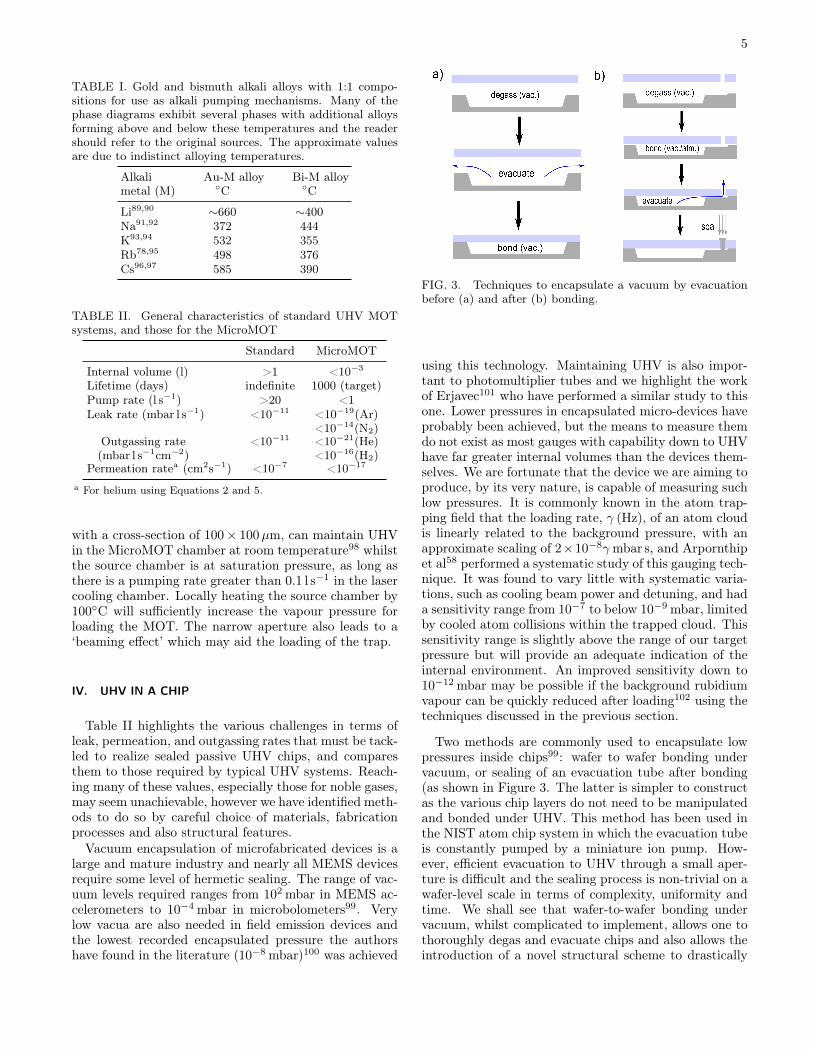
FIG. 3. Techniques to encapsulate a vacuum by evacuationbefore (a) and after (b) bonding.
using this technology. Maintaining UHV is also impor-tant to photomultiplier tubes and we highlight the workof Erjavec101 who have performed a similar study to thisone. Lower pressures in encapsulated micro-devices haveprobably been achieved, but the means to measure themdo not exist as most gauges with capability down to UHVhave far greater internal volumes than the devices them-selves. We are fortunate that the device we are aiming toproduce, by its very nature, is capable of measuring suchlow pressures. It is commonly known in the atom trap-ping field that the loading rate, γ (Hz), of an atom cloudis linearly related to the background pressure, with anapproximate scaling of 2×10⁻⁸γmbar s, and Arpornthipet al58 performed a systematic study of this gauging tech-nique. It was found to vary little with systematic varia-tions, such as cooling beam power and detuning, and hada sensitivity range from 10−7 to below 10−9 mbar, limitedby cooled atom collisions within the trapped cloud. Thissensitivity range is slightly above the range of our targetpressure but will provide an adequate indication of theinternal environment. An improved sensitivity down to10−12 mbar may be possible if the background rubidiumvapour can be quickly reduced after loading102 using thetechniques discussed in the previous section.
Two methods are commonly used to encapsulate lowpressures inside chips99: wafer to wafer bonding undervacuum, or sealing of an evacuation tube after bonding(as shown in Figure 3. The latter is simpler to constructas the various chip layers do not need to be manipulatedand bonded under UHV. This method has been used inthe NIST atom chip system in which the evacuation tubeis constantly pumped by a miniature ion pump. How-ever, efficient evacuation to UHV through a small aper-ture is difficult and the sealing process is non-trivial on awafer-level scale in terms of complexity, uniformity andtime. We shall see that wafer-to-wafer bonding undervacuum, whilst complicated to implement, allows one tothoroughly degas and evacuate chips and also allows theintroduction of a novel structural scheme to drastically

6
reduce leak rates discussed in Section IVC.
The choice of materials from which the micro-MOTcan be constructed is dependent on the sealing methodand the typical process environments. Suitable materialsfor UHV have negligible vapour pressures, low outgassingand permeability rates, and are mechanically strong andmachinable. Therefore metals such as stainless steel,aluminium, titanium and copper are predominant. TheMicroMOT would require optical access for the coolingbeams and fluorescence detection and so the chip mustinclude an optically transparent section, such as a glass orglass-ceramic wafer. Unfortunately there it a mismatchin the coefficients of thermal expansion (CTE) betweenglass and metal components which limit their baking,bonding, and operating temperatures. The exceptionsare low expansion alloys such as Kovar and Invar, theformer being specifically developed for glass-metal seals.Any remaining CTE mismatch can typically be allevi-ated with specially shaped sealing edges103. Neverthe-less, we find that the majority of metals104 do not havethe extremely low outgassing rates105,106 highlighted inTable II, and their glass-metal seals103 may not be ade-quately hermetic107, or are impractical to implement intothe microfabrication process (i.e. very high temperaturesfor extended periods). Alternative bonding methods arediscussed in Section IVC.
The MicroMOTs are likely to incorporate atom chipswhich commonly use silicon as a substrate due to its highthermal conductivity and the vast array of available semi-conductor processing techniques29. Coincidentally sili-con, as we shall see in the following sections, is a verysuitable UHV material: it has extremely low permeationand outgassing rates at room temperature, it has severalCTE-matched optical materials available, it is producedwith a high purity (to the 9N level), and can withstandhigh temperatures necessary for baking and bonding.The disadvantage of this material is its brittleness108, soonly small structures can be fabricated using specializedtechniques which is acceptable in our application, butnot for large scale vacuum systems. Several well studiedprocesses exist to clean silicon wafers and the lowest leakrates we have found for sealing technologies have beenfound for silicon-glass bonding (Section IVC). It is alsointeresting to note that polysilicon coatings are commer-cially available to reduce the outgassing rates of stainlesssteel chambers109. Another advantage is that silicon iscompletely non-magnetic, which is important for manip-ulating atoms, and is a poor electrical conductor whichreduces the deleterious effect of eddy currents during fastmagnetic field switching110 - a common issue with MOTs.Hence, in the following section we assume the chips arepredominantly constructed from silicon and glass, withadditional metal films for reflectors and getters.
A. Pumping
One cannot maintain a high vacuum without any formof pumping because no seal is perfect, all materials out-gas to some extent, and no material is impermeable to allgases. However, by reducing the above effects as much aspossible one can sustain vacuum with minimal pumping,especially in small volumes. As mentioned in the intro-duction we would like to maintain UHV with no activeor cryogenic pumping as such systems increase the totalsize, power requirements, and cost, not to mention thetime and money needed to develop chip scale analogues ofthese devices. Passive pumping elements take the form ofgetters which are metals, or alloys, that chemisorb typicalgases found in high vacuum, namely O2, CO, N2, and H2.Getters generally come in two varieties111: Evaporablegetters are metals which are heated until their increasedvapour pressure causes them to deposit on surroundingsurfaces. This traps residual gases under the depositedlayers, but the new surface also acts as a pump to im-pinging gases through chemisorption. Non-EvaporableGetters (NEGs) also chemisorb gases onto their surface,but in addition they absorb the reacted surface mate-rial into the getter bulk during heating (known as acti-vation). Both types keep pumping gases at room tem-perature, albeit at a reduced rate, providing their sur-faces are not saturated. NEGs activate at temperaturesranging around 200-800◦C, depending on their compo-sition, whereas evaporable getters need to be heated towell above 700◦C. Therefore the choice of NEGs for ourMicroMOT is obvious, and is further validated by itsadoption in the MEMs vacuum encapsulation industry.
Non-evaporable getters are made of Group IV/V met-als and alloys, such as Ti, Zr, V, Hf etc, and may alsoinclude metals such as Al and Fe. These are elementswith high oxygen solubility, high diffusivity, and high en-thalpy of adsorption for many gases found in vacuum112.When exposed to air, the surface of the NEG quicklypassivates forming oxides, nitrides and carbides in an 2-3 nm layer113. Heating the NEG in vacuum, known asactivation, causes these compounds to diffuse into thebulk leaving a fresh metallic surface pump. Typical oxy-gen solubilities for NEG compounds are on the order of10%, so a 1µm thin film can undergo ∼100 reactivationcycles after air exposure, however the pumping efficiencybegins to reduce after a few cycles114. This correspondsto an approximate total capacity of 1012 molecules percubic centimetre. Recent in-situ studies of NEG acti-vation with individual gases at temperatures above acti-vation indicate far higher capacities of the order of 105
monolayers of carbon monoxide115 due to the increasinglyuniform oxygen concentration in the film with tempera-ture. Hydrogen diffuses readily in the bulk, and so thecapacity is approximately two orders of magnitude higherthan surface pumped species at room temperature. Em-brittlement of the film at very high hydrogen concen-trations (above 1%) can result in delamination and so

7
should be avoided116. When NEGs are deposited as thinfilms they also act as outgassing barriers117, thus turninggas sources into pumps and greatly reducing the ultimatepressure. Noble gases and some hydrocarbons, such asmethane, are not pumped by NEGs at room tempera-ture. Therefore the MicroMOT will need to be sealedat UHV to ensure the majority of gases, especially thenobles, are evacuated prior to encapsulation.
The bonding techniques discussed in Section IVC re-quire temperatures up to 400◦C, which will lead to in-creased outgassing (see Section IVD) and a reductionof the NEG lifetime due to saturation. Moreover, re-activation of the getter to rejuvenate its pumping rateduring the sealed devices’ lifetime will lead to increasedoutgassing, permeation and possibly leakage. Thereforeit is prudent to use an NEG alloy with a very low activa-tion temperature, and high pumping rate and capacity.The beam lines of particle accelerators require XHV envi-ronments, and their very large volume presents an issuefor efficient and uniform pumping. Several decades ofresearch at CERN have been devoted to finding NEGsboth which activate during the chamber baking proce-dure (∼ 250◦C) and can also coat all internal surfaces118.Their findings have shown that sputtered TiZrV alloysof nearly equal ratios can be activated at 180◦C, andusing these coatings they have demonstrated the lowestroom temperature vacuum of 10−14 mbar119. The pump-ing rate of NEG films depends on their surface area andso the CERN team have also looked into the effects ofsubstrate and deposition parameters to increase pump-ing rates and capacities120. Additional attractive proper-ties of TiZrV NEG films are their high adhesion, thermaland vibration stability, resilience to standard wafer clean-ing processes, and commercial availability121. Table IIIshows the typical pumping rates and capacities of TiZrVNEG thin films whose values will be used in the follow-ing sections. Not all gases are pumped equally and somelead to reduced pumping speed of the NEG at high sur-face coverage (for example, CO reduces the pumping rateand capacity of H2 and N2) which are shown in Table III.This effect must be accounted for when calculating thelifetime of getter pumped devices. The unintentional in-corporation of noble gases in sputtered films can resultin outgassing which may endanger the vacuum122,123 andthis will be discussed in Section IVD. As a result, al-ternative methods, such as vacuum arc deposition113 ore-beam evaporation, should be considered.
Most gases only chemisorb on the NEG surface andshow negligible pumping after a monolayer is formed.Hydrogen is the exception as it diffuses throughout theentire bulk of the getter and so only the thickness of thefilm defines the capacity. There exists a thermal equi-librium between the absorption and desorption of hydro-gen from the NEG. This is dependent on the hydrogenconcentration124 and thus can be used to predict theresidual pressure in our devices. This value, known asthe disassociation pressure, follows Sieverts’ law and has
been measured for TiZrV films114. It was found to begiven by:
log10(PH2) = 2 log10(xH) + 14.324 − 8468
T(1)
Where PH2is in millibar, xH is the fraction of hydro-
gen in the film and T is the temperature in Kelvin. Wecan see that for a very saturated film (xH = 0.01) thepressure is negligible at room temperature (10−19 mbar)and only endangers the vacuum at temperatures above150◦C, at which point helium permeation through theglass wafer becomes equally problematic, as we shall seein Section IVB.
Earlier we dismissed evaporable getters on the basisof high operating temperatures and vapour phase gases.There is a new type of evaporable, or more specifically re-active, getter being investigated which uses alkali atomsas the gettering medium125–128. Early studies of alkalimetal dispensers showed that they improve the pumpingrate of the system76. Alkali and alkaline earth atoms willreact and bind strongly to the common residual gasesfound at UHV and therefore our devices may experi-ence an improvement of the vacuum during operation.Experiments have shown that the pumping rate for car-bon monoxide by lithium getter films is similar to TiZrVNEGs but with a capacity over 104 times greater. Thiswould be very advantageous to remove outgassed speciesduring bonding which could otherwise saturate TiZrVfilms. Most of the work on these reactive getters has fo-cused on lithium due to its low vapour pressure and abil-ity to form stable compounds with a number of gases. Wesuspect rubidium will provide some gettering, but not tothe extent of lithium due to the former’s high vapourpressure. For example, the disassociation pressure125of LiH at 300K is 10−21 mbar whereas that of RbH is10−7 mbar, only marginally less than rubidium vapourpressure60,129. It is expected, however, that pumpingof oxygen and carbon monoxide will be more effective.With its greater capacity and ability to pump additionalgases such as methane, which NEGs cannot, a lithiumgetter could replace, or complement, the NEG in the Mi-croMOT if the necessary vacuum cannot be pumped byNEGs alone130.
TABLE III. Typical pumping rates, sticking factors and ca-pacities of TiZrV NEGs at room temperature for a 1µm film.The values in parentheses indicate the pumping rate after car-bon monoxide saturation114. The capacities can be increasedby nearly an order of magnitude by heating the substrateduring deposition.
Gas Sticking Pumping Capacityfactor rate (l s−1cm−2) (cm−2)
H2 8× 10⁻³ 0.35 (0.1) > 1016
N2 1.5× 10⁻² 0.17 (0.1) 1.5× 10¹⁴
CO 0.7 8 1015
In the following sections we assume:

8
• An internal volume of 0.5 cm3.
• A surface area of 5 cm2.
• An NEG area of 1 cm2 with a thickness of 1µm.
B. Permeation
No material is absolutely impermeable to all gases, andso it is inevitable that they will diffuse through the wallsof any chamber and finally desorb into the vacuum. Weshall address the issue of permeation before the effectof outgassing and leaks as this is seen by many as thelimiting factor in achieving UHV in small, sealed, well-degassed volumes. Permeation is complex and requiresseveral processes to become a vacuum risk: 1) The gasmolecules in the external environment impinge on theouter surface of the chamber wall and physisorbed, 2)they disassociate if the surface enthalpy is greater thantheir bonds, 3) they are absorbed under the surface layerand diffuse through the bulk along the concentration gra-dient (Fick’s law), 4) the gas atoms must then overcomeany surface energy barriers, and 5) desorb from the sur-face directly or recombine with other ions to desorb as amolecule. These processes strongly depend on the typeof permeating gas and the chamber wall material. Forexample, noble gases will permeate glasses, but not mostmetals due to the latter’s more crystalline structure andweak surface interaction. As noble gases are not pumpedby NEGs their permeation is of greatest importance andwe shall devote the majority of this section to them, how-ever we will also discuss the effect of hydrogen as this isthe second fastest permeating gas (see Table V).
Surface effects, which will be discussed in Section IVD,tend to reduce the permeation rate so the simple processof bulk diffusion can be considered the limiting factorof permeation. The amount of gas flowing diffusivelyacross a membrane of area A and thickness d betweentwo regions of pressure Pext and Pint is
dQ
dt=KA(Pext − Pint)
d(2)
where K = DS is the permeation rate (cm2 s−1), D isthe diffusion constant (cm2 s−1) and S is the solubility(cm3 (STP)/cm3). Both D and S typically follow anArrhenius-type temperature dependence and the formeris quoted in the literature as
D(T ) = D0 exp
(−ED
kBT
)(3)
where ED is the diffusion energy, kB is the Boltzmannconstant and T is the temperature. The variation of Scan be much more complicated131, however over a lim-ited range of temperatures the Arrhenius form is ade-quate, and for most materials does not change apprecia-bly compared toD with temperature. Values of diffusion,
solubility and permeability of the materials highlightedin this study can be found compared to the common vac-uum materials, stainless steel and Pyrex, in Table IV.Equation 2 assumes the gas is already fully dissolved inthe membrane, which is not the case in thoroughly de-gassed materials. Therefore there is a period of time be-fore the gas will ‘break through’ to the evacuated volume,and in materials with very low diffusion rates this can beextremely long132. The pressure increase of a cavity ofvolume V at a time t due to a gas permeating through adegassed membrane is133:
Pc =ADSPext
V d
t− d2
6D− 2d2
π2D
∞∑m=1
(−1)me−m2π2Dt
d2
m2
(4)
Since the micro-MOT chambers will require at leastone optically transparent viewport the permeation of he-lium through glass will be a significant issue. The amor-phous network structure of glass forming oxides providechannels for helium to diffuse. Not all glasses are alikehowever, and the addition of ‘modifier’ molecules canact to plug the holes in the network, resulting in verylow permeation rates134. We aim to seal glass to sili-con and therefore must match CTEs to reduce stressesand therefore increase yield. Pyrex is the most commonglass bonded to silicon due to their comparable CTEsand its sodium content required for anodic bonding136(see Section IVC). This borosilicate glass is so highlypermeable to helium that we should expect to lose UHVseveral days after bonding (see Figure 4). Much workwas carried out in the 1960s and 1970s on the permeationrates of gases through glass, and the results showed thatAlumino-Silicate (AS) glass, those with approximately20% Al2O3 or more composition, had permeation rates
FIG. 4. The permeation rate of various 1mm optical wafersexposed to atmospheric helium after initial evacuation to10−10 mbar after complete degassing. We have calculated thevalues using Equation 4 and used the data for Corning 1720to define the properties of AS glass134,135.
9
five orders of magnitude lower than Pyrex134,137. Figure4 shows a comparison of the permeation rates of heliumthrough AS glass, Pyrex, fused silica, and Schott Zero-dur glass-ceramic, calculated using Equation 4. This lat-ter material is commonly used in UHV systems requiringlow permeation and its very low CTE makes it well suitedfor bonding. We can also see that Corning 1720 seriesAS glass is more than capable of maintaining vacuumfor our target time. Its CTE is well matched with sili-con to which is can be anodically bonded, albeit at muchhigher temperatures than Pyrex due to the low alkalicontent138–140.
Other AS glasses are commercially available, buttoo numerous to list here, and we mention that load-borate and soda-lime glasses also have low permeabil-ity characterisics. Silicon carbide141 has a very lowpermeability142, can be bonded to silicon143, and havebeen used for atom chips due to its transparency and highthermal conductivity144. Sapphire and glass-ceramicssuch as Spinel145 are likely to have extremely low per-meation rates, but yet again are not well CTE matched.Hard crystalline optical coatings may also reduce per-meation. Graphene, amongst its many other attrac-tive properties, has shown a permeability rate equal tobulk Pyrex, yet requiring only a single monolayer146.Unfortunately uniform coatings over large areas are asyet unavailable, but graphene-oxide may be a suitablealternative147.
Norton154 measured the permeation of other gasesthrough fused silica, as shown in Table V, and we can seethat, in general, larger molecules have lower permeationrates but can depend on surface interactions and solubil-ities (compare H2 and Ne). Hydrogen diffuses throughglass as a molecule131,152 and so, as shown in Table IV,it will have a far lower permeation rate than helium.Coupled with an order of magnitude lower atmosphericpartial pressure compared to helium, and the ability topump the gas with NEGs, hydrogen permeation can beneglected. Very little data is available on the hydrogenpermeability through AS glass and so we have used a scal-ing law by Souers et al150, the glass composition fromAltemose134, and the Pyrex solubility to calculate thediffusivity constants in Table IV.
TABLE V. Permeation of different gases159,160 through fusedsilica154.Gas Relative permeation Van der Waals
rate at 700◦C radius, nm
He 1 0.133H2 0.1 0.15Ne 0.02 0.141Ar <10−7 0.176
We now address the second material in our system:silicon. Measurements of helium permeation throughsilicon extrapolated from high temperatures show that,
like metals, silicon is practically impermeable to all no-ble gases. Using measured values for solubility cite-binns1993hydrogen,van1956permeation and typical at-mospheric helium content, we should not expect to finda single atom within a cubic centimetre of silicon. Wenote that recent studies161,162 looking at the hermetic-ity of glass frit encapsulation and other bonding meth-ods have indicated that helium permeation through sil-icon at room temperature may be more significant thanexpected. However, more work is required to confirmthis against the large bulk of research into helium bub-ble formation in silicon which agrees with the originallow permeation result163. Hydrogen, on the other hand,is known to permeate silicon albeit predominantly inatomic form at room temperature. This matter will bediscussed in great detail in Section IVD as the perme-ation rate is related to outgassing. The results in TableIV show that the permeation rate of hydrogen throughsilicon at room temperature is negligible.
C. Leaking
No seal is perfect as the bonding of materials will in-evitably lead to a route for gases to travel, via micro-channels and defects, or merely a local variation in thepermeation rate. Standard UHV systems predominantlyuse Conflat type seals which employ knife-edges to biteinto OHFC copper gaskets and join metal componentstogether, and ‘housekeeper’ type seals for glass-to-metalinterfaces. Commercial vacuum products quote leak ratesless than 10−11mbar l s−1 (STP), usually limited by theresolution of the leak detector164. These types of sealsare not suitable for wafer-level fabrication of vacuum en-capsulated micro-electronics and so several new methodshave been developed using chemically formed seals, orsimply relying on the attraction between perfectly flatsurfaces165. The small volume and long lifetime of manymicroelectronic chips may preclude the use of internalpumping mechanisms, meaning that the seals must haveextremely low leakage, more so than those demanded bystandard vacuum systems.
In Section IV we discussed the methods to encapsulatemicrofabricated vacuum devices and here we shall explorethe details of suitable bonding methods and their quality.We foresee the need for at least two bonding processes:one to bond the ‘atom chip’ to the structure wafer (sili-con to silicon, or gold to silicon), and another to bond theglass capping wafer to the structure layer (glass to sili-con). As many bonding technologies exist we will onlyconsider those which are well established, have demon-strated leak rates below 10−13 mbar l s−1 (air), and do notrequire temperatures above 400◦C so as to reduce out-gassing, stress, and protect chip components. We havenot considered low temperature indium bonding whichalthough initially seems promising can result in noble gasoutgassing unless special measures are undertaken. Also,it limits the activation of NEGs, may require several ad-

10
TABLE IV. Bulk diffusivities and solubilities (at STP) of helium and hydrogen in silicon, Pyrex (Corning 7740), aluminosilicate(Corning 1720), and stainless steel. We have also tabulated the permeation rates at 20◦C and 500◦C to compare values moreeasily.
Silicon148,149 Aluminosilicate134,150,151 Pyrex131,134,150–153 Stainless steel154,155
Heliuma
D0 (cm2s−1) 5.2× 10⁻³ 3.7× 10⁻⁴ 4.6× 10⁻⁴ Impermeable154,158
ED (eV) -0.82 -0.52 -0.28 -S0 (cm3 (STP) cm−3) 2.8× 10⁻⁴ 0.0016 0.005 -ES (eV) -0.77 - - -K (cm2s−1) @ 20◦C 3.2× 10⁻³⁴ 6.8× 10⁻¹⁶ 3.5× 10⁻¹¹ -
@ 500◦C 4.8× 10⁻¹⁷ 2.4× 10⁻¹⁰ 3.4× 10⁻⁸ -
Hydrogenb c
D0 (cm2s−1) 9.7× 10⁻³ 2.08× 10⁻⁷ K−1 1.4× 10⁻⁵ 1.2× 10⁻²
ED (eV) -0.48 -0.67 -0.24 -0.56S0 (cm3 (STP) cm−3) 90.4 0.038 0.038 0.3ES (eV) -1.86 -0.12 -0.12 -0.11K (cm2s−1) @ 20◦C 5.7× 10−40 6.1× 10⁻²³ 3.4× 10⁻¹⁶ 1.0× 10⁻¹⁴
@ 500◦C 1.2× 10⁻¹⁵ 4.3× 10⁻¹⁴ 2.4× 10⁻¹² 1.4× 10⁻⁷
a We are unable to find helium solubility in silicon data other than van Wieringen et al148 which is somewhat unreliable due to thelimited measurement range. In the tabulated values we have used that data with the theoretical energy of solution149 to calculate theprefactor. The diffusivity values are also theoretical but agree with experimental results148,156,157.
b We have assumed the same solubility for AS glass as for Pyrex due to the small variation found between glasses and the minimaltemperature variation152,153.
c Like helium, the commonly quoted values measured by van Wieringen et al148 are extrapolated from a narrow high temperature rangeand can be assumed to indicate the highest diffusion rate (see Section IVD).
ditional films to improve surface wetting, and the leakrate is not sufficiently low166.
Glass Frit
Glass frit bonding is a well established technique whichinvolves the deposition of a low melting point glass com-pound between two materials. The glass is heated first tooutgas the organic binder compounds, and is then raisedto the glass transition temperature which melts and sealsthe two surfaces upon cooling. The vacuum hermetic-ity of this technique has been explored extensively bySparks et al167, but no absolute leaks rates have beenquoted. We believe glass frit bonding to have a leakrate below 10−15 mbar l s−1 by considering the lifetime,internal volume, and pressure inferred by the integratedresonator’s Q-factor168. However, the pressure measured(∼ 10−3 mbar) is at the limit of the gauging techniqueand one does not know the residual pressure immediatelyafter bonding. Possible issues may include insufficientdegassing of the organic binder materials, limitations onpre-baking temperatures, incompatible CTEs (althoughthey can be engineered to match the application) andthe need for additional materials. Of the four bondingmethods presented here, glass frit has the least sensitiv-ity to surface quality and can be used to seal electricalfeedthroughs.
Eutectic Bonding
A eutectic alloy is one where the melting point of theconstituent materials is lowered on contact. For examplegold and silicon individually have melting points above1000◦C, but when they are pressed together they willmelt at 363◦C at their interface169,170. Subsequent cool-ing will form an alloy with high hermeticity and a strongbond. Other eutectic alloys exist, such as gold and tin171,but we highlight the gold-silicon system as many atomschips employ gold as a reflector and conductor. Thisbond has demonstrated the lowest leak rate that we havefound99, below 10−15 mbar l s−1. Pssible disadvantagesinclude the need for multilayer films to prevent inter-layer diffusion170, the requirement of inert gas storagebefore bonding to prevent the native oxide growth on sil-icon, and the temperature restrictions post bonding, asfurther heating remelts the alloy and degrades the bond.
Anodic Bonding
Anodic bonding occurs between an oxide formingmetal (or semiconductor) and an alkali containing glass,by heating the two materials together (300-500◦C) withthe simultaneous application of a high voltage (100-1000V) across the interface136,138. The mobility of thealakli ions (typically sodium or lithium) in the glass isincreased with temperature and they are pulled awayfrom the interface by the electric potential. The resid-ual non-bridging oxygen atoms at the interface then

11
bond with the silicon. The high electric potential gra-dient has the additional effect of pulling the two surfacesinto intimate contact which overcomes surface inhomo-geneities. The two materials (usually silicon and borosil-icate glass) must have very flat surfaces, below 10 nm,and be CTE matched to avoid stress fractures duringcooling. Hermeticity measurements show that the leakrate is below 10−14 mbar l s−1, with few residual gasesother than oxygen, which is produced during bondingat the inner seam. This residual gas source can be sig-nificant, especially in small evacuated volumes, and sogetter films are mandatory (see Section IVD). The leakrate measurements172,173 included the effect of the bond-ing area around the cavity and found no variation, fromwhich we infer that the seal is absolutely hermetic andpossibly limited only by permeation.
Direct Bonding
Direct bonding is the result of the attractive Van derWalls forces between atomically flat surfaces. Semicon-ductor and glass wafers are routinely produced with therequired flatness and this technique requires no addi-tional materials, does not release gases (unlike anodicand frit bonding), and is hermetic173 (Leak rates be-low 10−14 mbar l s−1). Unfortunately, for the silicon-silicon direct bond, very high post-annealing tempera-tures (up to 1000◦C) are required to ensure a high bond-ing yield and to reduce voids. This latter effect is dueto gases desorbing between the surfaces which becomestrapped. Bonding in vacuum produces fewer voids, dueto a thorough degassing before sealing, to the point thatstrong bonds form at room temperature without theneed for post annealing174. The extremely flat surfacesare difficult to retain during processing and even sub-micron particles will result in debonding. CTE-matchedglass-silicon direct bonding occurs with lower annealingtemperatures175, and the glass can absorb gases releasedbetween the interface.
To summarize the bonding techniques, there are sev-eral methods to obtain reliable leak rates lower than10−14 mbar l s−1 and even below 10−15 mbar l s−1. An-odic and direct bonds may even be absolutely hermetic,limited by permeation, but their absolute leak rates werebeyond the sensitivity of their measurements. Eutecticbonding has shown the lowest measured leak rates and isa reliable and low outgassing method. Glass frit may alsohave equally low leak rates, but the residual gas pressurereleased during bonding is unknown.
QL =V∆P
∆t(5)
Using Equation 5 we can calculate the highest permis-sible leak rate for a gas at atmospheric pressure leakinginto our specified volume of V = 0.5 cm3, such that the
pressure does not rise by 50% (∆P = 0.5 × 10⁻¹⁰ mbar)over ∆t = 1000days, to be 3 × 10⁻²² mbar l s−1. Thisrate seems unachievable, but we must consider that somegases are pumped away by the NEGs and so may permita higher leak rate, and many gases have low atmosphericpartial pressures. For example the partial pressure of he-lium in the atmosphere is 5 × 10⁻³ mbar and so one canpermit a leak rate176 of 1.5 × 10⁻¹⁷ mbar l s−1.Reactive gas leakage is limited by the pump rate and ca-pacity of the NEG films. In light of this we may modelthe lifetime of the device due to NEG saturation usingthe following formula:
dPc
dt=
1
V
(QL − LPPc(1 − θ)k
)(6)
Where Pc is the internal pressure (mbar), QL is theleak rate (mbar l s−1), LP is the pumping rate of the get-ter (l s−1), θ is the fractional surface coverage, and k isthe order of desorption. The effect of surface coverage onpumping depends on the gas/surface chemistry, temper-ature, and surface geometry (flat, granular, etc.). Thistopic is too extensive to detail here but can be foundin most surface science graduate texts177. We find thatthe Langmuir adsorption isotherm, (1 − θ)k, models themajority of data on NEG pumping rates114 adequatelyfor our purposes due to the low surface coverage. Thepressure inside the cavity will drop to base value:
Pbase =QL
Lp(7)
As noted earlier, the effect of saturation by some gases(for example carbon monoxide) reduces the pumpingspeed of other gases114 which we do not take into ac-count dynamically in the model, but assume the lowestpumping speed as the ‘worst case scenario’.
There is a sharp drop in pumping speed at saturationallowing us to simplify the lifetime calculation. By as-suming that the pumping rate is constant until the NEGhas reached its capacity of CG (moles), at which point itubruptly drops to zero, and by setting θ = 1 in Equation6 and using the ideal gas formula, we find an approximatevalue for the maximum permissible leak rate:
QL(max) =CGRT
τL(8)
where R is the ideal gas constant, T (K) is the temper-ature and τL (sec) is the lifetime. If we assume a pump-ing speed for nitrogen, the most abundant atmosphericgas, of 0.1 l s−1, a capacity of 1014 molecules, with a life-time of 1000 days: the maximum permissible leak rateis 5×10⁻¹⁵ mbar l s−1 with Pbase = 5×10⁻¹⁴ mbar. Thiscan be achieved with reliable bonding from all the meth-ods detailed earlier. Note that Equation 8 is independentof both the pumping rate and background pressure be-cause it assumes them to be at equilibrium, therefore one

12
FIG. 5. The internal pressure (blue) and NEG cover-age (red) with an atmospheric leak of nitrogen at a rate6.5×10−15 mbar l s−1 (air) calculated using Equation 6. Thehorizontal dashed line indicates the target pressure and thevertical line the result of Equation 8. The cavity is initiallyat 10−10 mbar.
must use this equation alongside Equation 7 to ensure thecorrect base pressure. Figure 5 compares the numericalsolution of Equation 6 with the approximate value fromEquation 8 and we find perfect agreement. We note thatthe capacity is that for a single monolayer and so the life-time can simply be extended through reactivation cycles.Hydrogen diffuses into the bulk and so reactivation doesnot increase the getter lifetime, but the NEG capacityfor hydrogen can be two to three orders of magnitudegreater (see Table III), so is not as much of a concern.
The atmosphere contains several noble gases99 includ-ing argon (9.3mbar), neon (1.8×10⁻² mbar), and he-lium (5×10⁻³ mbar), where the values in parenthesesare the atmospheric partial pressures. Their leak ratesare proportional to (T/M)0.5, where T is the temper-ature in Kelvin and M is their mass, hence heliumleaks at the fastest rate and is often used in hermetic-ity tests178 known as ‘Helium Bombing’. If we assumea leak rate which is proportional to the pressure differ-ential across the bond, the effect of argon, due to itsrelatively high atmospheric partial pressure will be mostsignificant. The maximum permissible leak rate for ar-gon is 1×10⁻¹⁹ mbar l s−1. The significance of this gashas been mentioned in the literature179, but is generallyignored as helium permeation through glass is consid-ered to be a more pressing issue. If we compare thelowest measured leak rate for the bonding methods of10−15 mbar l s−1 (air) we find all the noble gases endan-ger UHV, however helium and neon leakage need only bereduced by factor of 15 and 25, respectively, which maybe possible with thicker bonding seams or external bar-rier coatings, whereas argon must be reduced by nearly104.
There is, however, a very simple scheme to reduce the
FIG. 6. Numerical solution of Equations 9 for various ratios ofmoat/cavity volume. We assume argon is leaking from the at-mosphere, and the quoted leak rate is for each bond seam (air-to-moat and moat-to-cavity) adjusted to atmospheric pres-sure to compare with literature values. The horizontal dottedline represents a 50% rise in pressure from an initial value of10−10 Pa, and the vertical line indicates 1000 days. In thissimulation Vm = 0.25Vc would meet the target property withan overall leak rate of 6×10⁻²¹ mbarm3s−1 (air).
leak rate by several orders of magnitude: Simply by plac-ing the vacuum chamber inside another. This can beachieved practically by introducing a buffer cavity, ormoat, within the seam such that the slow leakage intothe moat results in an even slower leakage into the mainvacuum cavity180. This can be modeled by the followingformulae and solved numerically:
dPb
dt=
1
Vb(Cab(Pa − Pb) − Cbc(Pb − Pc)) (9)
dPc
dt=Cbc(Pb − Pc)
Vc(10)
where Pi is the pressure, Vi is the volume, and Cij is theconductance between i, and j, in which the subscriptsi, j = a, b, c refer to the air, buffer, and cavity, respec-tively. We have independently modelled this effect andfound stark, but advantageous, differences from the orig-inal study by Gan et al180. We suspect that an error wasmade in tabulating their results, which also clarifies theirunexplained lifetime increase for 100mbar cavities. If weassume a main cavity volume of 0.5 cm3 and a moat vol-ume of 0.05 cm3 we can reduce the leakage rate by factorof 2×10⁵ as shown in Figure 6. This allows us to usebonds with leak rates in the range of 10−14 mbar l s−1(air) which is technically feasible with all the bondingtechniques considered earlier, and also reduces the NEGlimitations on reactive gases. The moat does not have tobe bonded at UHV as the model shows very little varia-tion below an initial moat pressure of 10−6 mbar.

13
D. Outgassing
Outgassing is the release of gas from a material’s sur-face and bulk. We distinguish this from permeation inthat the latter assumes a completely degassed material,whereas outgassing is the result of gases that are dif-ficult to remove from the bulk. These have either en-tered from diffusion during storage, processing, or fromthe production of the material itself. Cleanliness is ofutmost importance in achieving UHV and we assumeall components have been through standard wafer clean-ing processes, such as an RCA and ozone plasma. Thislatter technique has also been shown to improve bondstrengths and reduce temperatures direct and anodicbonding181,182. We shall not go into further detail re-garding cleaning here and direct the interested reader tothe references183–186. We do highlight that detergentswere found to remove vanadium from the NEG films andso should be avoided187.
Outgassing is the largest source of gas in well-sealedUHV systems and so usually defines the lowest basepressure for a specific pumping rate Lp according toEquation 7. Hydrogen is the dominant gas at UHV,for which the NEGs have a pumping rate on the or-der of 0.1 l s−1cm−2, and so to achieve 10−10 mbar onemust ensure the outgassing rate is below 10−11mbar l s−1.There is no standard model for predicting the outgassingproperties of all materials as many different mechanismsare involved188,189 but can be essentially split into twosources: surface and bulk. We assume that the surfacesare clean in that common contaminates such as organicshave been thoroughly removed leaving only atmosphericand some processing species, namely water, hydrogen,carbon monoxide, and noble gases. We can calculate thesurface desorption rate using:
dN
dt=Nθk
τsexp
(−ES
kBT
)(11)
where N is the surface density (molecules cm−2), θ isthe fractional surface coverage, k is the desorption or-der, τs is the sojourn time (typically 10−13 s), and ES
is the desorption energy190. Typically, outgassing fromthe surface occurs at the fastest rate as physisorbed, orweakly chemisorbed gases, have low desorption energies.Strongly bound molecules (ES> 1.1 eV) can in general beignored as they do not appreciably desorb from surfacesat room temperature, whereas weakly bound species(ES< 0.7 eV) can be pumped away quickly. Moleculesin the middle of this range are difficult to pump outin a practical time and so high temperature baking isrequired191. We shall refer to this as the ‘outgassing en-ergies range (OER)’.
Outgassing of reactive species from the bulk is morecomplex than simple diffusion. Gases, such as hydrogen,diffuse ionically and can form bonds with the bulk ma-terial or impurities in a process known as trapping. Ions
may also recombine within the solid and become trappedin lattice defects, and any ion reaching the surface needsto recombine in order to desorb. At low surface coveragethis latter, second order, step can be the limiting rate.Many of the transport processes are activated and so onlyoccur at elevated temperatures. This can result in unre-liable predictions when extrapolating high temperaturedata down to room temperature. The effects are furthercomplicated by surface oxides or nitrides which, in gen-eral, act to reduce outgassing rates by providing a barrierlayer192–194. Noble gases, on the other hand, only traveldiffusively through the bulk and easily desorb from sur-faces at all temperatures due to their weak interaction.All of the effects outlined above act to only reduce theoutgassing rate compared to a simple diffusion model andtherefore one can assume bulk diffusion as the most sig-nificant factor. If we assume purely diffusive outgassingfrom the material bulk, and that it is degassed from bothsides, then we can use the rate calculated by Lewin191 fora ‘slab’ geometry:
QOG
A=
8x0D
d
∞∑m=0
exp
[−Dt
(π(2m+ 1)
d
)2]
(12)
Where D is diffusion rate, A is the surface area, d isthe thickness and x0 is the initial concentration of thegas in the bulk. For a non-disassociative gas x0 = SP ,where S is the solubility and P is the partial pressureof the gas. For a disassociative gas the concentration isproportional to P 0.5 instead, and the solubility units areadjusted accordingly. By using values for diffusion foundexperimentally, effects such as trapping are automaticallyincluded into the model. As highlighted by Chuntonov et
al195 the increase of outgassing during the high tempera-ture bonding process can cause the NEG film to becomesaturated and limit the lowest obtainable vacuum andlifetime of the device. To calculate actual lifetime includ-ing the effect of bonding we can consider the reductionof getter capacity by the number of molecules releasedduring bonding, and using Equation 8 to find:
τL =T
Q
(CGR− τB
TB
∑gases
QB
)(13)
where T is room (or operating) temperature, TB isthe bonding temperature, τB is the bonding time (sec-onds), Q is the outgassing rate at T , and QB is the out-gassing rate at TB . We have assumed the temperaturesare changed instantaneously and the bonding period isshort enough not to affect the operating outgassing rate.The same formula can be used to predict the increasedoutgassing due to reactivation of the NEG during theMicroMOT lifetime. The effect of the bonding can beneglected if:
η =τBQB
RCGTB<< 1 (14)

14
Assuming an NEG with a hydrogen capacity of 10−7
moles (xH = 0.01), a bonding time of τB = 3600s ata temperature of TB = 400◦C, and we wish to keepη = 0.1, the bonding outgassing rate must be QB <10−7 mbar l s−1cm−2. If this is the result of bulk diffu-sion which scales as
Q =D(T )
D(TB)QB = QB exp
(−ED(T − TB)
kBTBT
)(15)
and we use a diffusion energy in the middle of the OERof ED = 0.9 eV, then one must reduce room temperaturehydrogen outgassing rate to QB < 10−16 mbar l s−1cm−2.Equation 15 also applies for surface desorption (for whichED = ES). Gases such as carbon monoxide, for whichthe NEG has only a single monolayer capacity, requireoutgassing rates over a hundred times lower comparedto hydrogen without continuous reactivation. These areextremely low outgassing rates and are the main hurdlein obtaining very low vacua in microelectronic devices. Inthe following subsection we explore the outgassing ratesof the main gases found at UHV - H2, CO, as well as noblegases - from the materials considered for the MicroMOTand we have tabulated measured and theoretical valuesfor outgassing rates in Table VI.
Hydrogen
Hydrogen can be a major issue in semiconductor de-vices and so extensive work has been carried out to un-derstand its interaction with silicon215–219. The mostcommon and earliest citation in the literature is to thework done by van Wieringen and Warmoltz148 (which weshall refer to vWW). Their diffusivity and solubility datawas taken at very high temperatures (967-1207◦C) andthese values are shown in Table IV. Extrapolation downto room temperature is fraught with possible errors as hy-drogen readily dissociates upon diffusing into the bulk,interacting with the silicon lattice and impurities in var-ious forms. Figure 7 shows the results of subsequent dif-fusion studies and one can see the large variation in mea-surements in the literature. Advances in understandinghave shown that hydrogen migration through bulk siliconpredominantly occurs in atomic form at room tempera-ture with an activation barrier of ∼ 0.5 eV, but can re-combine into a dimer which is then trapped by an barrierof 0.8 − 1.2 eV. Exact values are difficult to predict anddepend on various doping and impurity levels, growthmethods, defects and lattice orientations, and even quan-tum effects220. The vWW diffusivity results are consis-tently higher than every subsequent measurement andcan be taken as the upper limit in our analysis221.
Whichever diffusivity one uses, the vWW solubilityresults extrapolate to 10−10 molecules per cubic cen-timetre at room temperature under 1 bar of H2 andso there should be no hydrogen whatsoever within thebulk. Other measurements have found agreement witha very low value , with the highest at only a few
hundred hydrogen atoms per cubic centimetre at roomtemperature222–224. Using any one of these solubilitiesdoes not alter the permeation values in Table IV by amore than a factor of two or three.
Standard semiconductor processing, such as mechan-ical polishing, HF etching, plasma treatments etc, canresult in far higher levels of hydrogen close to thesurface215. Several studies have found values as high as1018 molecules per cubic centimetre and drops signifi-cantly after a depth of one micron225. This concentra-tion will lead to outgassing rates of 10−7 mbar l s−1cm−2,using Equation 12 and the vWW diffusivity scal-ing law, but can be completely degassed to below10−30 mbar l s−1cm−2 within an hour under vacuum asshown in Figure 8, limited by surface recombination.Moreover, surface oxides and nitrides act as efficient per-meation barriers192–194. Hydrogen bound on the sili-con surface has very high desorption energy226,227 (above1.8 eV) such that the desorption rate from one mono-layer coverage would be below 10−22 mbar l s−1cm−2 us-ing Equation 11. Thermal desorption studies227 showthat most hydrogen complexes can be desorbed from sil-icon by annealing at 600◦C.
Hickmott228 studied the interaction between hydrogenand glass and found that the hot filament of the ioniza-tion gauge had a detrimental effect on determining theresidual gas content at UHV. He noted that hydrogenwas desorbed at the two distinct activation energies of0.29 eV and 1.08 eV. The former is so low that it willdesorb completely at room temperature under vacuum,whereas the latter requires baking above 400◦C. Spec-troscopic studies by Hickmott showed that after a hightemperature bake the main residual gases were water andcarbon monoxide. Todd229 measured the residual watercomposition in a variety of glasses and found negligibleoutgassing (∼ 10−23 mbar l s−1cm−2) in AS glass afterhigh temperature baking. This low outgassing rate is dueto the strong Si-H and Si-OH bonds. Using the valuesfrom Table IV and Equation 12 to calculate the lowest hy-drogen outgassing rate from AS glass, as shown in TableVI, we find remarkable agreement between the theoreticalvalue of just over 10−17 mbar l s−1cm−2 and experimentalresult230,231 of just below232 10−16 mbar l s−1cm−2.
Noble gases
Noble gases cannot be removed once the MicroMOTsare sealed and so must be completely degassed from allcomponents before bonding. As discussed in Section IVBnegligible levels of noble gases, specifically helium, shouldbe found in silicon unless additional data corroboratesa recent study161. Noble gases in glasses are expectedto reach concentrations of 10 ppb when exposed to at-mosphere, which will outgas from the bulk diffusively.Figure 9 shows the results of degassing AS glass usingEquation 12, and we see that a thin slab can be com-

15
FIG. 7. The large scatter in data for diffusion of hydrogen through silicon148,196–214. We have only plotted data for hydrogendiffusion (no isotopes) and have indicated the type of silicon where known. The solid black line is the commonly quoted vWWdiffusion rate.
pletely degassed easily. This would scale proportionallyto the area when wafer level degassing is required.
The last materials in our chips are metals such as goldfor the atom chip and those for the NEG. Noble gasesdo not permeate most metals and so one should be ableto ignore these materials, however the method of theirdeposition is important: Sputtered thin films have beenfound to incorporate large quantities of argon, as thisprocess gas is used to remove the metal atoms from thesputter target. The argon is then buried in the growingthin film and permeates to the surface along dislocationsand pores, as well as via self-diffusion. Where possiblefilms should be deposited by vacuum arc deposition113or e-beam evaporation which do not require additionalgases. In situations where sputtering is unavoidable sev-eral modifications can be made to reduce contaminationby this gas source including122,123: lowering the sput-ter gas pressure, increasing the substrate temperature,reducing the deposition rate, post annealing, and finallychanging to a heavier gas. Using this last modification byreplacing argon with krypton has been shown to reducethe gas incorporation by a factor of 103 or even lower,but moving to xenon shows little improvement123. Mea-surements of TiZrV NEG films have detected kryptonoutgassing rates233 at the sensitivity limit of the detector- down to 10−19 mbar l s−1cm−2 after several activations-which is still too high for our device, but this could befurther reduced with higher temperature anneals.
Carbon monoxide
Carbon monoxide is the second most significant gas atUHV. Due to its relatively large size (compared to he-lium or hydrogen) diffusion through the bulk will be neg-ligible and so carbon monoxide is largely a surface out-gassing species234. Studies looking at the residual gasesin glass have shown that the carbon monoxide concentra-tions vary widely235 and it is difficult to obtain repeat-able results. In addition, this also depends on glass type,processing history, and the effects of ionization cathodes.We do not know the desorption energy for carbon monox-ide on glass, but due to the latter’s low reactivity weexpect carbon monoxide to only be physisorbed and soquickly degassed. Similar conclusions have been notedin photodesorption measurements236. One study look-ing at the effect of breaking glass substrates in vacuumfound that the carbon monoxide level remained constant,but carbon dioxide quickly decreased237. This was at-tributed to the reaction with residual hydrogen form-ing methane, which was seen to increase. A carefulstudy238 avoiding the effects of gauges measured carbonmonoxide outgassing rates from stainless steel less than6×10−17 mbar l s−1cm−2, three orders of magnitude lessthan hydrogen.
Thermal desorption studies of carbon monoxide re-leased from silicon surfaces are few, but show that thethermal desorption energy is below 0.5 eV239 and soshould be degassed easily. Photodesorption and plasmacleaning have also been shown to efficiently remove car-bon and oxygen contamination from silicon surfaces.

16
FIG. 8. The theoretical outgassing rate of hydrogen for 1mmthick silicon (dashed line) and AS glass (solid line) for threebaking temperatures. We have assumed AS glass is diffusionlimited and calculated the rate using Equation 12 and valuesfrom Table IV after exposure to 1 bar hydrogen (i.e. immer-sion into water). We have calculated the rate for silicon usinga summation of diffusion (Equation 12) from the bulk as wellas considering the higher concentration at the surface (seetext), and also recombination-limited surface desorption us-ing Equation 11 (k = 2) with values from Gupta et al227. Theroom temperature silicon outgassing shows an initially highrate due to diffusion of the high concentration near the surfaceand is eventually limited by surface desorption of the dihy-dride surface species (as are the higher temperature bakes).
Other gases
Methane is also found in UHV environments and isthought to be produced from reactions on the high tem-perature electrodes of ionization gauges, so should notbe an issue in our gauge-less MicroMOTs. It may also beformed from reactions between carbon monoxide and hy-drogen during their diffusion on NEG or glass surfaces237,as mentioned before. TiZrV NEGs do not pump methaneand so this gas should be completely evacuated beforethe MicroMOT is sealed, otherwise one must use reac-tive getters. Other organic species have been found inencapsulated MEMs-type devices which are likely due toinsufficent cleaning or residual gases prior to sealing99,240.
Should anodic bonding be used to seal the chips, oxy-gen will be released along the inner bonding edges wherethe voltage is high and no silicon exists to bond withthe non-bridging oxygen atoms136,172,241. Predicting theamount of oxygen released is unreliable due to the lack ofdata and the effects of bonding parameters, chip dimen-sions, and increased outgassing at raised temperatures.By analyzing the few studies on this subject172,241,242we estimate 1013 to 1014 molecules per millimetre innerbonding circumference. For our MicroMOT design thiscan lead to a monolayer coverage of oxygen on the NEGsand result in saturation. It should be noted that oxy-gen penetrates the NEG surface resulting in a capacity
FIG. 9. The He outgassing rate from 1mm thick alumi-nosilicate glass slab at various temperatures after storage inatmosphere (5 ppm He content), calculated with Equation 12.The black dashed line indicates the target outgassing rate.
of about five monolayers114. Therefore it is importantto maintain the chip at high temperatures after bondingto absorb the oxidized NEG layers into the bulk. Oncerubidium is released into the chip it will quickly oxidizewith any remaining oxygen forming Rb2O, which alsoreacts exothermically with water and hydrogen formingstable hydroxides and hydrides which do not contaminatevacuum.
E. Vacuum discussion
We have identified all the main sources of residual gaseswhich could threaten our sealed UHV environment. Wehave seen that helium permeation through glass can bereduced to a negligible level with the use of aluminosili-cates and could further be improved with optical coatingssuch as graphene. Leaking through bonds must be severalorders of magnitude higher than has been measured, butcan be sufficiently improved by incorporating a ‘moat’within the bonding seam. We also note that leakage canbe further reduced by coating the inner edges of bondingseams with NEG films and by applying a barrier coatingon the outer edges of the device. Several bonding tech-niques are available and we highlight eutectic and directbonding as the most suitable methods due to their lowoutgassing and high hermeticity, with anodic bonding asa suitable alternative if the oxygen released during bond-ing can be pumped away. Lowering the temperatures ofthese bonding techniques should be investigated as theycan reduce the outgassing limitations by two or three or-ders of magnitude171,174,175,181,243–248.
The greatest hurdle we are left with is to reduce out-gassing. This can be tackled in two ways: 1) improvethe pumping rate and capacity of the getter films, and 2)

17
TABLE VI. Lowest and typical room temperature outgassingrates for 2mm thick materials. The theoretical values (Th.)have been estimated using Equation 12 and Figure 8 witha 10 hr 250◦C vacuum bake for ‘typical outgassing’ and anadditional 1 hr 600◦C vacuum bake for ‘lowest outgassing’.
Outgassing rate Lowest Typical(mbar l s−1cm−2)
Silicona 10−30 (Th.) 10−24 (Th.)Aluminosilicate 10−17 10−16 (Th.b)Pyrex 10−14 10−10
Stainless steel 10−15c 10−12
a Theoretical values taken from Figure 8.b Using values from Table IVc Thinner materials have lower outgassing rates and Nemanič etal249 have demonstrated 10−17 with 150µm foil.
reduce the outgassing rate by extensive degassing proce-dures and careful choice of materials.
It has been shown that the pumping rate of NEGs isdifficult to improve even with reactive lithium getters,however the latter retains a constant pumping rate irre-spective of its history. NEGs are more straightforwardto deposit, can be used to coat surfaces to reduce out-gassing and are stable in air. Reactive getters need to bedeposited under vacuum and could result in unwantedcoating on components in the chamber. However, theyhave far higher capacities and can pump gases such asmethane, which NEGs cannot. Therefore we see a com-bination of NEGs and reactive getters as a good compro-mise with the former activated during bonding and thelatter activated after bonding.
For the second method to tackle outgassing wehave seen in Table VI that at room temperature thematerials we have chosen for the device are morethan adequate once degassed to achieve the roomtemperature outgassing rate of 10−13 mbar l s−1cm−2.When we consider the outgassing during bonding ataround 400◦C it can increase by eight orders of mag-nitude and put stricter room temperature rates ofless than 10−16 mbar l s−1cm−2 for bulk gettered gasessuch as hydrogen, 10−18 mbar l s−1cm−2 for surface get-tered gases such as carbon monoxide, and less than10−21 mbar l s−1cm−2 for non-gettered noble gases. Wecan see in Table VI that silicon outgassing is likely to benegligible compared to AS glass whose rate matches ourtarget. When calculating this value we assumed a diffu-sion energy of 0.9 eV. We can now be confident that ASglass will be the major source of hydrogen so if we usea more realistic value of 0.79 eV (Table IV) we lower ourtarget to 10−15 mbar l s−1cm−2, which is certainly achiev-able. Carbon monoxide outgassing is difficult to predictbut we expect it to be far lower than hydrogen, as foundin stainless steel238. We have seen that noble gases maybe sufficiently removed from the chamber material withrealistic baking parameters and by using the separatedwafer fabrication method shown in Figure 3, one can en-sure the optimum baking regime for each material.
V. PROTOTYPE MICROMOT
We are now at the stage where we can design a pro-totype MicroMOT and the fabrication process which iscurrently under development and will be characterizedat a later date. As discussed in Section II we assume aG-MOT type geometry using a 10mm diameter gratingstructure and a cavity volume of 15×15×3mm3 to avoidlight scattering off sidewalls. Around 90% of the beamoverlap volume is within 2.5mm of the grating surface,and so this is a reasonable choice of height and is alsofeasible to fabricate from silicon using deep reactive ionetching, wet etching, machining, or powder blasting250.We have consciously avoided designing the MicroMOTaround a single application or manipulation technique,e.g. free-falling atom interferometers, or BECs on atomchips. This is because the MicroMOT will likely needto be adapted for the specific task, so we have chosen asimple generic design to demonstrate what is possible.
The chip is formed of four chambers: a large sciencechamber for cooling and manipulating the atoms, anatom source chamber in which to hold the alkali dis-pensers, an alkali getter/LIAD/peltier chamber, and areactive getter chamber. The source chamber is con-nected to the science chamber by a very thin channel(1×0.1×0.1mm) to restrict the vapour flow, but exper-imental data will be needed to optimize these dimen-sions. The top 2mm thick capping wafer is anti-reflectioncoated and is anodically or direct bonded to the sili-con ‘cavity wafer’. The thickness of the glass layer isdetermined by several factors including the permeationrates, bondability, structural integrity and price. Thiswafer incorporates a moat within the bonding region onboth sides to reduce argon leakage. The reflector layeris coated by a thin alumina layer to prevent alkali corro-sion of the gold and is eutectically bonded to the cavitywafer. We have not shown the quadrupole magnetic fieldcoils as these are trivial to implement and may simply bebonded, or deposited, onto the top and bottom externalsurfaces, or could be approximated with a double loopon single surface251.
Following extensive cleaning procedures, the glass andsilicon wafers are first bonded in vacuum so that oxy-gen released can be removed if anodic bonding is used.An NEG thin film is sputtered on the internal sidewallsand onto some of the bottom layer (with the reflectormasked off) to provide the largest NEG area and reduceoutgassing. The remaining reflector layer is then eutecti-cally bonded under UHV after high temperature bakingto desorb hydrogen, carbon monoxide and noble gases.
Table VII provides a detailed summary of dimensionsand an estimation on the vacuum properties of the deviceusing values calculated in this study. We can see that thelifetime of the device is determined by the argon leakage,but is nearly an order of magnitude greater than our tar-get. The extremely low outgassing rate of AS glass results

18
FIG. 10. Prototype design of a miniaturized magneto-opticaltrap incorporating all the elements discussed in the text. Di-mensions are 20×24×5mm3.
in negligible outgassing after bonding such that the basepressure is in the XHV regime for an essentially unlim-ited lifetime. Practically, the lifetime and base pressurewill be determined by the atom source and the ability topump away the vapour. The incorporation of high sur-face area materials will inevitably result in significantlyincreased outgassing, but porous silicon may be the bet-ter candidate due to the inherently low outgassing rateof silicon and the ability to desorb hydrogen with UVlight252.
VI. DISCUSSION AND CONCLUSIONS
We have shown that it is feasible to maintain UHV,and even XHV, environments for extended periods in-side sealed chips using materials and methods borrowedfrom the semiconductor industry. However, it is neces-sary to highlight the assumptions we have made if thesetype of devices are to become a realistic technology. Agreat emphasis has been made on degassing the materialsat temperatures up to 600◦C to ensure a sufficiently lowoutgassing rate once sealed. For the bulk materials dis-cussed this is certainly possible, but more sophisticateddevices are likely to have additional components, such asmicro-Peltier coolers, detectors, field emission tips (foractive pumping or ionization), or even light sources (suchas UV LEDs for LIAD), which can be sensitive to ex-treme temperatures. Moreover, thin films, such as goldon silicon, can diffuse at moderate temperatures if addi-tional barrier layers are not used170. In these situationsone must use lower temperature degassing, such as UVdesorption or plasma cleaning, and also develop lowertemperature bonding methods171,174,175,181,243–248.
The very low leak rates we have predicted are possi-ble by a combination of hermetic bonding and additionalmoat cavities. We have assumed that the materials to bejoined are reliably homogeneous and intact (e.g. perfect
crystallinity in the case of silicon) but in reality fabri-cation processes may lead to defects which can resultin additional leakage routes such as microcracks, crystalplane dislocations, surface defects, or thin oxide films.Surface barrier films, NEG coatings and stress-relief an-nealing can reduce these effects but these possible sourcesof leakage are still worth bearing in mind.
We have used the large amount of data on hydrogendiffusion in silicon to predict that it has a very low out-gassing rate. We find that this rate is consistently lowwhichever values we use from the literature, especiallyafter a high temperature bake for several hours, and sowe are confident in the estimate. However, as mentionedin Section IVD, there is no absolutely reliable method topredict the outgassing rate from real materials and thesimple diffusion-limited model is only useful to an orderof magnitude at best, especially when considering the mi-gration of reactive species such as hydrogen. This can beseen with studies looking at the outgassing of stainlesssteel, where the diffusion limited model produces reason-able estimate for low temperature bakes (below 300◦C),but generally fails to predict the effect of very high tem-peratures. This is usually attributed to the effect of sur-face oxides which are more stable during low tempera-ture baking and act as diffusion barriers253. Thereforewe expect silicon to have a very low outgassing rate butprobably higher than the value stated in Table VI. Ex-perimental studies focusing specifically on outgassing arerequired. We have used measured values for AS glassoutgassing, but glasses are notorious for producing vari-able results254 so it is necessary to perform additionaloutgassing studies on the specific glass one uses to en-sure suitability. For the sake of bevity we have limitedour discussions to silicon and glasses but there are likelyto be many other suitable materials, most noteably ce-ramics which are equally suitable.
In conclusion, the aim of this study was to prove thatMagneto-Optical Traps can be miniaturised and inte-grated into devices capable of leaving the laboratory.We have shown that recent advances in microfabrica-tion techniques and materials can lead to sealed chamberswith microlitre volumes that maintain UHV for at least1000 days using only passive pumping elements. TheMOT geometry can be miniaturized to use a single laserbeam, patterned reflectors, and atom source. Controlledby a number of methods including LIAD, integrated coldfingers, conductance channels and several pumping mech-anisms. The main issues to maintain sealed UHV envi-ronments are the need for extremely low leakage bonds,low outgassing materials, and also negligible noble gasoutgassing from chamber walls and sputtered films. Wehope that this work motivates the development of ul-tracold quantum technology which has a vast number ofpractical applications and promises to be a fruitful tech-nology in a number of fields.
We would like to acknowledge Tim Freegarde, DavidSmith, Erling Riis, Aidan Arnold, Joe Cotter, Wolfgang

19
TABLE VII. Expected vacuum properties of the prototype MicroMOT in atmosphere at 20◦C.
Internal volume (cm3) 0.65 including subchambersSurface area (cm2) 7.8 2.6 glassNEGa area (cm2) 3.3 all sides and some of the reflector surfaceGlass thickness (cm) 0.2Moat volume (cm3) 0.03 1×0.5 mm trench within each bonding seamBonder base pressure (mbar) 10−9 equal H2 and CO, negligible noble gasesBonding parameters 1 hr at 400◦C typical eutectic bond
Gas source (mbar l s−1) Surface pumped (CO) Bulk pumped (H2) Noble gas
Permeationb - 1.3×10⁻²³ 7.3×10⁻²³
Leakagec 1.9×10⁻²³ 3.8×10⁻²⁴ 2.3×10⁻²²
Outgassingd 4.5×10⁻¹⁷ 2.6×10⁻¹⁶ < 10−24
Base pressuree (mbar) 10−18 10−15 -Lifetime (days to reach 1.5×10⁻¹⁰ mbar) 106 109 3200a Surface capacity of 5×10¹⁴ molecules cm−2 and bulk capacity of 7.5×10¹⁶ molecules cm−2 (1µm film with xH = 0.01).b The permeation rates are calculated using the breakthrough time from Equation 4 substituted into Equation 5.c Bond leak rate (air) of 10−15 mbar l s−1 for 2 bonding seams (top wafer and bottom wafer). We have assumed the carbon monoxideleak is from atmospheric carbon dioxide.
d As the carbon monoxide outgassing rate is unknown we have assumed a value which is ten times less than hydrogen as discussed in thetext as a worst case scenario.
e The base noble gas pressure will be equal to the residual level in the bonding chamber.
Reinert, and Kai Bongs, for their helpful and insightfuladvice and ideas in the development of this study. Thiswork was supported by the Royal Academy of Engineer-ing, EPSRC, the Royal Society, and DSTL.
1B. Barrett, P.-A. Gominet, E. Cantin, L. Antoni-Micollier,A. Bertoldi, B. Battelier, P. Bouyer, J. Lautier, and A. Lan-dragin, arXiv preprint arXiv:1311.7033 (2013).
2J. Kitching, S. Knappe, and E. A. Donley, Sensors Journal,IEEE 11, 1749 (2011).
3N. Hinkley, J. A. Sherman, N. B. Phillips, M. Schioppo, N. D.Lemke, K. Beloy, M. Pizzocaro, C. W. Oates, and A. D. Ludlow,Science 341, 1215 (2013).
4S. M. Dickerson, J. M. Hogan, A. Sugarbaker, D. Johnson, andM. A. Kasevich, arXiv preprint arXiv:1305.1700 (2013).
5B. Canuel, F. Leduc, D. Holleville, A. Gauguet, J. Fils,A. Virdis, A. Clairon, N. Dimarcq, C. J. Bordé, A. Landragin,et al., Physical review letters 97, 010402 (2006).
6C. J. Bordé, Metrologia 39, 435 (2002).7F. Yver-Leduc, P. Cheinet, J. Fils, A. Clairon, N. Dimarcq,D. Holleville, P. Bouyer, and A. Landragin, Journal of OpticsB: Quantum and Semiclassical Optics 5, S136 (2003).
8M. Edwards, Nature Physics 9, 68 (2013).9D. Budker and M. Romalis, Nature Physics 3, 227 (2007).10N. Behbood, F. Martin Ciurana, G. Colangelo, M. Napolitano,M. W. Mitchell, and R. J. Sewell, Applied Physics Letters 102,173504 (2013).
11S. Wildermuth, S. Hofferberth, I. Lesanovsky, S. Groth,P. Kruger, J. Schmiedmayer, and I. Bar-Joseph, Applied physicsletters 88, 264103 (2006).
12D. Oblak, P. G. Petrov, C. L. G. Alzar, W. Tittel, A. K. Ver-shovski, J. K. Mikkelsen, J. L. Sørensen, and E. S. Polzik,Physical Review A 71, 043807 (2005).
13M. Napolitano, M. Koschorreck, B. Dubost, N. Behbood,R. Sewell, and M. W. Mitchell, Nature 471, 486 (2011).
14L. Pezzé and A. Smerzi, Physical review letters 102, 100401(2009).
15J. Appel, P. J. Windpassinger, D. Oblak, U. B. Hoff, N. Kjær-gaard, and E. S. Polzik, Proceedings of the National Academyof Sciences 106, 10960 (2009).
16C. Monroe, Nature 416, 238 (2002).
17A. Kozhekin, K. Mølmer, and E. Polzik, Physical Review A 62,033809 (2000).
18L.-M. Duan, M. Lukin, J. I. Cirac, and P. Zoller, Nature 414,413 (2001).
19S. Diehl, A. Micheli, A. Kantian, B. Kraus, H. Büchler, andP. Zoller, Nature Physics 4, 878 (2008).
20H. Marion, F. P. Dos Santos, M. Abgrall, S. Zhang, Y. Sortais,S. Bize, I. Maksimovic, D. Calonico, J. Grünert, C. Mandache,et al., Physical review letters 90, 150801 (2003).
21S. Dimopoulos, P. W. Graham, J. M. Hogan, and M. A. Kase-vich, Physical review letters 98, 111102 (2007).
22C. J. Bordé, Philosophical Transactions of the Royal SocietyA: Mathematical, Physical and Engineering Sciences 363, 2177(2005).
23J. P. Dowling and G. J. Milburn, Philosophical Transactions ofthe Royal Society of London. Series A: Mathematical, Physicaland Engineering Sciences 361, 1655 (2003).
24J. Pritchard and S. Till, “UK Quantum Technology Landscape2014,”.
25T. Könemann, W. Brinkmann, E. Göklü, C. Lämmerzahl,H. Dittus, T. Van Zoest, E. Rasel, W. Ertmer, W. Lewoczko-Adamczyk, M. Schiemangk, et al., Applied Physics B 89, 431(2007).
26R. Geiger, V. Ménoret, G. Stern, N. Zahzam, P. Cheinet, B. Bat-telier, A. Villing, F. Moron, M. Lours, Y. Bidel, et al., Naturecommunications 2, 474 (2011).
27T. Van Zoest, T. Müller, T. Wendrich, M. Gilowski, E. Rasel,W. Ertmer, T. Könemann, C. Lämmerzahl, H. Dittus, A. Vo-gel, et al., International Journal of Modern Physics D 16, 2421(2007).
28S. Groth, P. Kruger, S. Wildermuth, R. Folman, T. Fern-holz, J. Schmiedmayer, D. Mahalu, and I. Bar-Joseph, AppliedPhysics Letters 85, 2980 (2004).
29J. Reichel and V. Vuletic, Atom Chips (John Wiley & Sons,2010).
30D. Stick, W. Hensinger, S. Olmschenk, M. Madsen, K. Schwab,and C. Monroe, Nature Physics 2, 36 (2005).
31M. Brownnutt, G. Wilpers, P. Gill, R. Thompson, and A. Sin-clair, New Journal of Physics 8, 232 (2006).
32Symmetricom SA.45 chip scale atomic clock.33S. Knappe, V. Gerginov, P. Schwindt, V. Shah, H. Robinson,

20
L. Hollberg, and J. Kitching, Optics Letters 30, 2351 (2005).34M. de Angelis, M. Angonin, Q. Beaufils, C. Becker, A. Bertoldi,K. Bongs, T. Bourdel, P. Bouyer, V. Boyer, S. Dörscher, et al.,Procedia Computer Science 7, 334 (2011).
35S. Chu, Reviews of Modern Physics 70, 685 (1998).36K. Salit, J. Sebby-Strabley, K. Nelson, and J. Kriz, in Frequency
Control Symposium (FCS), 2012 IEEE International (IEEE,2012) pp. 1–4.
37B. Xu, X. Chen, J. Wang, and M. Zhan, Optics Communica-tions 281, 5819 (2008).
38V. Shah, M. Mescher, R. Stoner, V. Vuletic, and R. Lutwak,arXiv preprint arXiv:1111.5890 (2011).
39E. A. Salim, J. DeNatale, D. M. Farkas, K. M. Hudek, S. E.McBride, J. Michalchuk, R. Mihailovich, and D. Z. Anderson,Quantum Information Processing 10, 975 (2011).
40R. Folman, P. Krüger, D. Cassettari, B. Hessmo, T. Maier, andJ. Schmiedmayer, Physical Review Letters 84, 4749 (2000).
41S. Wildermuth, P. Krüger, C. Becker, M. Brajdic, S. Haupt,A. Kasper, R. Folman, and J. Schmiedmayer, Physical ReviewA 69, 030901 (2004).
42K. Lee, J. Kim, H. Noh, and W. Jhe, Optics letters 21, 1177(1996).
43J. Arlt, O. Marago, S. Webster, S. Hopkins, and C. Foot, Opticscommunications 157, 303 (1998).
44M. Vangeleyn, P. F. Griffin, I. McGregor, E. Riis, andA. Arnold, in Lasers and Electro-Optics 2009 and the EuropeanQuantum Electronics Conference. CLEO Europe-EQEC 2009.European Conference on (IEEE, 2009) pp. 1–1.
45M. Trupke, F. Ramirez-Martinez, E. Curtis, J. Ashmore,S. Eriksson, E. Hinds, Z. Moktadir, C. Gollasch, M. Kraft,G. Vijaya Prakash, et al., Applied physics letters 88, 071116(2006).
46S. Pollock, J. Cotter, A. Laliotis, and E. Hinds, Optics Express17, 14109 (2009).
47S. Pollock, J. Cotter, A. Laliotis, F. Ramirez-Martinez, andE. Hinds, New Journal of Physics 13, 043029 (2011).
48This can be mitigated with background free imaging255.49C. Nshii, M. Vangeleyn, J. Cotter, P. Griffin, E. Hinds, C. Iron-side, P. See, A. Sinclair, E. Riis, and A. Arnold, Nature nan-otechnology (2013).
50J. Lee, J. Grover, L. Orozco, and S. Rolston, JOSA B 30, 2869(2013).
51G. W. Hoth, E. A. Donley, and J. Kitching, Optics Letters 38,661 (2013).
52Several studies have shown the scaling laws for various beamoverlap volumes, however we highlight that none have consid-ered the effect of unsymmetrical volumes for which reducing onedimension could be beneficial in wafer-level microfabrication byreducing chamber size whilst maintaining a large capture vol-ume.
53L. Huet, M. Ammar, E. Morvan, N. Sarazin, J.-P. Pocholle,J. Reichel, C. Guerlin, and S. Schwartz, in International Quan-tum Electronics Conference (Optical Society of America, 2011)p. I1188.
54T. Kovachy, J. M. Hogan, D. M. Johnson, and M. A. Kasevich,Physical Review A 82, 013638 (2010).
55W. D. Phillips and H. Metcalf, Physical Review Letters 48, 596(1982).
56W. D. Phillips, J. V. Prodan, and H. J. Metcalf, JOSA B 2,1751 (1985).
57T. Liebisch, E. Blanshan, E. Donley, and J. Kitching, PhysicalReview A 85, 013407 (2012).
58T. Arpornthip, C. Sackett, and K. Hughes, Physical Review A85, 033420 (2012).
59P. Berthoud, A. Joyet, G. Dudle, N. Sagna, and P. Thomann,EPL (Europhysics Letters) 41, 141 (1998).
60D. A. Steck, “Rubidium 87 D line data,” (2001).61L.-A. Liew, S. Knappe, J. Moreland, H. Robinson, L. Hollberg,and J. Kitching, Applied Physics Letters 84, 2694 (2004).
62F. Vecchio, V. Venkatraman, H. Shea, T. Maeder, and P. Ryser,
Procedia Engineering 5, 367 (2010).63S. Radhakrishnan and A. Lal, in Solid-State Sensors, Actuators
and Microsystems, 2005. Digest of Technical Papers. TRANS-DUCERS’05. The 13th International Conference on, Vol. 1(IEEE, 2005) pp. 23–26.
64L.-A. Liew, J. Moreland, and V. Gerginov, Applied physicsletters 90, 114106 (2007).
65F. Gong, Y.-Y. Jau, K. Jensen, and W. Happer, Review ofscientific instruments 77, 076101 (2006).
66S. Bartalini, I. Herrera, L. Consolino, L. Pappalardo, N. Marino,G. D’Arrigo, and F. Cataliotti, The European Physical Jour-nal D-Atomic, Molecular, Optical and Plasma Physics 36, 101(2005).
67Www.alvatec.com.68P. Griffin, K. Weatherill, and C. Adams, Review of scientificinstruments 76, 093102 (2005).
69A. Douahi, L. Nieradko, J. Beugnot, J. Dziuban, H. Maillote,S. Guerandel, M. Moraja, C. Gorecki, and V. Giordano, Elec-tronics Letters 43, 33 (2007).
70Integrating high power focused beams into a chip scale systemwould not be trivial and the beam must be moved once sectionsof the dispenser are depleted. An alternative heating methodcould include induction heating.
71M. Stephens, R. Rhodes, and C. Wieman, Journal of appliedphysics 76, 3479 (1994).
72In that study they found that Pyrex took an order of magnitudelonger to cure than sapphire. The glass used in this study islikely to have properties in between these materials.
73The effect of hard optical coatings on the glass, such as MgF2
to reduce reflections or ITO for heating, may also reduce theeffectiveness of glass as a pump.
74H. Bottner, in Thermoelectrics, 2002. Proceedings ICT’02.Twenty-First International Conference on (IEEE, 2002) pp.511–518.
75D. R. Scherer, D. B. Fenner, and J. M. Hensley, Journal ofVacuum Science & Technology A: Vacuum, Surfaces, and Films30, 061602 (2012).
76P. della Porta, C. Emili, and J. Hellier, in IEEE Conference ontube techniques (IEEE, 1968).
77Scherer et a l75 state that NEGs do not pump rubidium at all,whereas della Porta et al76 state that alkali atoms do not affectthe pumping speed for other gases. We suspect there is somepumping due to the high reactivity of alkali atoms with metalsand with most adsorbed gases.
78A. Pelton, Bulletin of Alloy Phase Diagrams 7, 139 (1986).79L. Torralbo-Campo, G. D. Bruce, G. Smirne, and D. Cassettari,arXiv preprint arXiv:1312.6442 (2013).
80A. Hatakeyama, M. Wilde, and K. Fukutani, arXiv preprintcond-mat/0512451 (2005).
81K. Rębilas and M. J. Kasprowicz, Physical Review A 79, 042903(2009).
82S. Villalba, H. Failache, and A. Lezama, Physical Review A 82,56902 (2010).
83S. Atutov, R. Calabrese, V. Guidi, B. Mai, A. Rudavets,E. Scansani, L. Tomassetti, V. Biancalana, A. Burchianti,C. Marinelli, et al., Physical Review A 67, 053401 (2003).
84B. Anderson and M. Kasevich, Physical Review A 63, 023404(2001).
85D. Xiong, F. Wang, X. Li, T.-F. Lam, and D. Wang, arXivpreprint arXiv:1303.0333 (2013).
86S. Du, M. B. Squires, Y. Imai, L. Czaia, R. Saravanan,V. Bright, J. Reichel, T. Hänsch, and D. Z. Anderson, PhysicalReview A 70, 053606 (2004).
87A. Burchianti, C. Marinelli, A. Bogi, J. Brewer, K. Rubahn,H.-G. Rubahn, F. Della Valle, E. Mariotti, V. Biancalana,S. Veronesi, et al., EPL (Europhysics Letters) 67, 983 (2004).
88S. Villalba, H. Failache, and A. Lezama, Physical Review A 81,032901 (2010).
89A. Pelton, Journal of Phase Equilibria 7, 228 (1986).90J. Sangster and A. Pelton, Journal of phase equilibria 12, 447
21
(1991).91A. Pelton, Bulletin of Alloy Phase Diagrams 7, 136 (1986).92J. Sangster and A. Pelton, Journal of phase equilibria 12, 451(1991).
93A. Pelton, Journal of Phase Equilibria 7, 23 (1986).94A. Petric and A. Pelton, Journal of phase equilibria 12, 29(1991).
95A. Pelton and A. Petric, Journal of phase equilibria 14, 368(1993).
96A. Pelton, Bulletin of Alloy Phase Diagrams 7, 19 (1986).97J. Sangster and A. Pelton, Journal of phase equilibria 12, 443(1991).
98J. F. O’Hanlon, A user’s guide to vacuum technology (JohnWiley & Sons, 2005).
99V. Lindroos, M. Tilli, A. Lehto, and T. Motooka, Handbook ofsilicon based MEMS materials and technologies (Elsevier, 2009).
100W. Choi, B. Ju, Y. Lee, S. Jeong, N. Lee, M. Sung, and M. Oh,Journal of The Electrochemical Society 146, 400 (1999).
101B. Erjavec, Vacuum 64, 15 (2001).102P. Willems and K. Libbrecht, Physical Review A 51, 1403
(1995).103A. Roth, Vacuum sealing techniques (Springer, 1994).104The lowest outgassing rates for metals are tabulated by
Redhead231 with high temperature annealed stainless steel andOFHC copper displaying outgassing rates between 10−15 and10−16 mbar l s−1cm−2.
105W. Perkins, Journal of Vacuum Science and Technology 10, 543(1973).
106S.-w. Zhang, Z.-j. Zhang, C.-h. XU, and L. Wang, Journal ofNortheastern University (Natural Science) 8, 027 (2008).
107To be more precise, the authors cannot find absolute leak rate ofthese seals in the literature and commercial glass-metal, or glass-ceramic, seals only state leak rates ‘below 10−10 mbar l s−1’.However, our discussions with commercial vacuum tube man-ufacturers indicate that the leak rate for metal-ceramic sealscould be as low as 10−18 mbar l s−1 or lower.
108K. E. Petersen, Proceedings of the IEEE 70, 420 (1982).109Http://www.silcotek.com/silcod-technologies/SilcoGuard-high-
purity-coating/.110C. Dedman, K. Baldwin, and M. Colla, Review of Scientific
Instruments 72, 4055 (2001).111For a more detailed up to date sub-division of getter types see
Chuntonov et al195.112C. Benvenuti, J. Cazeneuve, P. Chiggiato, F. Cicoira, A. Es-
cudeiro Santana, V. Johanek, V. Ruzinov, and J. Fraxedas,Vacuum 53, 219 (1999).
113R. Sharma, N. Mithal, K. Bhushan, D. Srivastava, H. Prab-hakara, S. Gadkari, J. Yakhmi, V. Sahni, et al., in Journal ofPhysics: Conference Series, Vol. 114 (IOP Publishing, 2008) p.012050.
114P. Chiggiato and P. Costa Pinto, Thin Solid Films 515, 382(2006).
115M. Bender, H. Kollmus, M. Bellachioma, and W. Assmann, Nu-clear Instruments and Methods in Physics Research Section B:Beam Interactions with Materials and Atoms 268, 1986 (2010).
116K. Jousten, Handbook of vacuum technology (John Wiley &Sons, 2008).
117C. Benvenuti, P. Chiggiato, F. Cicoira, and V. Ruzinov, Vac-uum 50, 57 (1998).
118A. Prodromides, C. Scheuerlein, and M. Taborelli, Vacuum 60,35 (2001).
119C. Benvenuti, A. Escudeiro Santana, and V. Ruzinov, Vacuum60, 279 (2001).
120A. Prodromides and F. Lévy, Non-Evaporable Getter Thin FilmCoatings for Vacuum Applications, Tech. Rep. (CERN, 2002).
121SAES getters and Nanogetters.122S. Amorosi, M. Anderle, C. Benvenuti, S. Calatroni, J. Carver,
P. Chiggiato, H. Neupert, and W. Vollenberg, Vacuum 60, 89(2001).
123B. Window, Journal of Vacuum Science & Technology A: Vac-
uum, Surfaces, and Films 11, 1522 (1993).124C. Liu, L. Shi, S. Xu, Z. Zhou, S. Luo, and X. Long, Vacuum
75, 71 (2004).125K. Chuntonov and J. Setina, Journal of Alloys and Compounds
455, 489 (2008).126K. Chuntonov, A. Ivanov, and D. Permikin, Journal of Alloys
and Compounds 456, 187 (2008).127K. Chuntonov, J. Setina, A. Ivanov, and D. Permikin, Journal
of Alloys and Compounds 460, 357 (2008).128K. Chuntonov, A. Ivanov, and D. Permikin, Journal of Alloys
and Compounds 471, 211 (2009).129J. Sangster and A. Pelton, Journal of phase equilibria 15, 87
(1994).130One could consider using lithium as the trapped species instead.131J. F. Shackelford, P. L. Studt, and R. M. Fulrath, Journal of
Applied Physics 43, 1619 (1972).132A common value quoted in the literature is the ‘characteristic
time’ tc = d2
6D, this is time it takes to produce a constant flow,
not for the gas to initially break through and so overestimatesthe time it take for the permeating gas to effect the vacuum.
133W. Rogers, R. Buritz, and D. Alpert, Journal of AppliedPhysics 25, 868 (1954).
134V. Altemose, Journal of Applied Physics 32, 1309 (1961).135J. Covino and J. M. Bennett, Laser-Gyro Materials Studies,
Tech. Rep. (DTIC Document, 1986).136K. Knowles and A. Van Helvoort, International materials re-
views 51, 273 (2006).137J. Shelby and R. J. Eagan, Journal of the American Ceramic
Society 59, 420 (1976).138G. Wallis and D. I. Pomerantz, Journal of Applied Physics 40,
3946 (1969).139P. Baine, L. Quinn, B. Lee, S. Mitchell, B. Armstrong, and
H. Gamble, Thin solid films 296, 141 (1997).140L. Spangler and K. Wise, in Solid-State Sensor and Actuator
Workshop, 1988. Technical Digest., IEEE (IEEE, 1988) pp.140–143.
141P. M. Sarro, Sensors and Actuators A: Physical 82, 210 (2000).142P. Jung, Journal of nuclear materials 191, 377 (1992).143C. Tudryn, S. Schweizer, R. Hopkins, L. Hobbs, and A. J.
Garratt-Reed, Journal of the Electrochemical Society 152, E131(2005).
144A. Shevchenko, M. Heiliö, T. Lindvall, A. Jaakkola, I. Tittonen,M. Kaivola, and T. Pfau, Physical Review A 73, 051401 (2006).
145P. Trocellier, S. Agarwal, and S. Miro, Journal of Nuclear Ma-terials 445, 128 (2014).
146J. S. Bunch, S. S. Verbridge, J. S. Alden, A. M. van der Zande,J. M. Parpia, H. G. Craighead, and P. L. McEuen, Nano letters8, 2458 (2008).
147R. Nair, H. Wu, P. Jayaram, I. Grigorieva, and A. Geim, Science335, 442 (2012).
148A. Van Wieringen and N. Warmoltz, Physica 22, 849 (1956).149M. Alatalo, M. Puska, and R. Nieminen, Physical Review B
46, 12806 (1992).150P. Souers, I. Moen, R. Lindahl, and R. Tsugawa, Journal of the
American Ceramic Society 61, 42 (1978).151S. Steward, Review of hydrogen isotope permeability through
materials, Tech. Rep. (Lawrence Livermore National Lab., CA(USA), 1983).
152N. Kurita, N. Fukatsu, H. Otsuka, and T. Ohashi, Solid stateionics 146, 101 (2002).
153H. Laska, R. Doremus, and P. Jorgensen, The Journal of Chem-ical Physics 50, 135 (1969).
154F. J. Norton, Journal of Applied Physics 28, 34 (1957).155P. Marin, M. Dialinas, G. Lissillour, A. Marraud, and A. Re-
boux, Vacuum 49, 309 (1998).156P. Jung, Nuclear Instruments and Methods in Physics Research
Section B: Beam Interactions with Materials and Atoms 91, 362(1994).
157C. Griffioen, J. Evans, P. D. Jong, and A. V. Veen, NuclearInstruments and Methods in Physics Research Section B: Beam

22
Interactions with Materials and Atoms 27, 417 (1987).158C.-A. Chen, Y. Sun, Z. Huang, C. Liu, and S. Wu, Physica
Scripta 2003, 97 (2003).159M. Mantina, A. C. Chamberlin, R. Valero, C. J. Cramer, and
D. G. Truhlar, The Journal of Physical Chemistry A 113, 5806(2009).
160S. Batsanov, Inorganic materials 37, 871 (2001).161D. Sparks, Journal of Micromechanics and Microengineering 23,
015016 (2013).162D. Sparks, J. Mitchell, and S. Lee, Journal of Sensor Technology
3, 101 (2013).163G. F. Cerofolini, F. Corni, S. Frabboni, C. Nobili, G. Ottaviani,
and R. Tonini, Materials Science and Engineering: R: Reports27, 1 (2000).
164Ultra low helium leak detectors using the accumulation methodand NEG pumps have measured leak rates256 as low as10−15mbar l s−1 .
165S. H. Christiansen, R. Singh, and U. Gosele, Proceedings of theIEEE 94, 2060 (2006).
166R. Straessle, M. Pellaton, C. Affolderbach, Y. Pétremand,D. Briand, G. Mileti, and N. de Rooij, Journal of AppliedPhysics 113, 064501 (2013).
167D. Sparks, S. Massoud-Ansari, and N. Najafi, in Micromachin-ing and Microfabrication (International Society for Optics andPhotonics, 2004) pp. 70–78.
168D. Sparks, J. Trevino, S. Massoud-Ansari, and N. Najafi, Jour-nal of Micromechanics and Microengineering 16, 2488 (2006).
169R. Wolffenbuttel and K. Wise, Sensors and Actuators A: Phys-ical 43, 223 (1994).
170S. Lani, A. Bosseboeuf, B. Belier, C. Clerc, C. Gousset, andJ. Aubert, Microsystem technologies 12, 1021 (2006).
171C. C. Lee, C. Y. Wang, and G. Matijasevic, Components, Hy-brids, and Manufacturing Technology, IEEE Transactions on16, 311 (1993).
172S. Mack, H. Baumann, U. Gösele, H. Werner, and R. Schlögl,Journal of the Electrochemical Society 144, 1106 (1997).
173S. Mack, H. Baumann, and U. Gosele, in Micro Electro Me-chanical Systems, 1997. MEMS’97, Proceedings, IEEE., TenthAnnual International Workshop on (IEEE, 1997) pp. 488–493.
174U. Gosele, H. Stenzel, T. Martini, J. Steinkirchner, D. Conrad,and K. Scheerschmidt, Applied physics letters 67, 3614 (1995).
175T.-K. Chuang, A. Usenko, and J. Cites, ECS Transactions 33,501 (2010).
176The relative conductance, or leak rate, of non-interacting gases,is proportional to the square root of their masses. Hence he-lium will leak 2.6 times faster than nitrogen. For the followingcalculation we has assumed the average molecular mass of is 29.
177G. Attard and C. Barnes, Surfaces (Oxford University PressOxford, UK, 1998).
178S. Millar and M. Desmulliez, Sensor Review 29, 339 (2009).179W. Reinert, D. Kahler, and G. Longoni, in Electronic Packaging
Technology Conference, 2005. EPTC 2005. Proceedings of 7th,Vol. 1 (IEEE, 2005) pp. 6–pp.
180Z. Gan, D. Huang, X. Wang, D. Lin, and S. Liu, Sensors andActuators A: Physical 149, 159 (2009).
181S.-W. Choi, W.-B. Choi, Y.-H. Lee, B.-K. Ju, M.-Y. Sung, andB.-H. Kim, Journal of The Electrochemical Society 149, G8(2002).
182O. Zucker, W. Langheinrich, M. Kulozik, and H. Goebel, Sen-sors and Actuators A: Physical 36, 227 (1993).
183W. Kern, Journal of the Electrochemical Society 137, 1887(1990).
184W. Kern et al., Handbook of semiconductor wafer cleaning tech-nology, Vol. 623 (Noyes Park Ridge, NJ, 1993).
185J. R. Vig, Journal of Vacuum Science & Technology A: Vacuum,Surfaces, and Films 3, 1027 (1985).
186S. Franssila, Introduction to microfabrication (Wiley. com,2010).
187M. Taborelli, Cleaning and surface properties, Tech. Rep.(CERN, 2006).
188R. Elsey, Vacuum 25, 299 (1975).189R. Elsey, Vacuum 25, 347 (1975).190Typically k = 1 for high surface coverage, but increases to 2
when desorption is recombination limited at low coverage.191G. S. Lewin, Fundamentals of Vacuum Science and Technology
(McGraw-Hill, USA, 1965).192W. Perkins and D. Begeal, The Journal of Chemical Physics 54,
1683 (1971).193V. Nemanič, P. J. McGuiness, N. Daneu, B. Zajec, Z. Siketić,
and W. Waldhauser, Journal of alloys and compounds 539, 184(2012).
194N. Nickel, W. Jackson, I. Wu, C. Tsai, and A. Chiang, PhysicalReview B 52, 7791 (1995).
195K. A Chuntonov and S. P Yatsenko, Recent Patents on MaterialsScience 6, 29 (2013).
196S. Koveshnikov, S. Nosenko, and E. Yakimov, physica statussolidi (a) 120, 391 (1990).
197Y. Kamiura, M. Yoneta, and F. Hashimoto, Applied physicsletters 59, 3165 (1991).
198C. Seager and R. Anderson, Applied physics letters 53, 1181(1988).
199K. Schmalz and K. Tittelbach-Helmrich, physica status solidi(a) 113, K9 (1989).
200M. Vergnat, S. Houssaini, C. Dufour, A. Bruson, G. Marchal,P. Mangin, R. Erwin, J. Rhyne, and C. Vettier, EPL (Euro-physics Letters) 14, 457 (1991).
201X.-M. Tang, J. Weber, Y. Baer, and F. Finger, Physical ReviewB 42, 7277 (1990).
202N. Johnson, C. Nebel, P. Santos, W. Jackson, R. Street,K. Stevens, and J. Walker, Applied physics letters 59, 1443(1991).
203C. Seager, R. Anderson, and D. Brice, Journal of appliedphysics 68, 3268 (1990).
204R. Newman, J. Tucker, A. Brown, and S. McQuaid, Journal ofapplied physics 70, 3061 (1991).
205A. Majumdar, S. Balasubramanian, V. Venkataraman, andN. Balasubramanian, Journal of applied physics 82, 192 (1997).
206B. Sopori, X. Deng, J. Benner, A. Rohatgi, P. Sana, S. Estre-icher, Y. Park, and M. Roberson, Solar Energy Materials andSolar Cells 41, 159 (1996).
207C. Herrero, M. Stutzmann, A. Breitschwerdt, and P. Santos,Physical Review B 41, 1054 (1990).
208N. Johnson and C. Herring, Physical Review B 46, 15554 (1992).209R. Rizk, P. De Mierry, D. Ballutaud, M. Aucouturier, and
D. Mathiot, Physical review B 44, 6141 (1991).210S. Fabian, S. Kalbitzer, C. Klatt, M. Behar, and C. Langpape,
Physical Review B 58, 16144 (1998).211Y. Huang, Y. Ma, R. Job, and A. Ulyashin, Journal of applied
physics 96, 7080 (2004).212W. Hansen, S. Pearton, and E. Haller, Applied Physics Letters
44, 606 (1984).213M. Capizzi and A. Mittiga, Applied physics letters 50, 918
(1987).214A. Mogro-Campero, R. Love, and R. Schubert, Journal of The
Electrochemical Society 132, 2006 (1985).215S. J. Pearton, J. W. Corbett, and T. Shi, Applied Physics A
43, 153 (1987).216J. Chevallier and M. Aucouturier, Annual Review of Materials
Science 18, 219 (1988).217E. E. Haller, Semiconductor Science and Technology 6, 73
(1991).218S. Myers, H. Birnbaum, J. Corbett, G. DeLeo, S. Estreicher,
E. Haller, P. Jena, N. Johnson, R. Kirchheim, and S. Pearton,Reviews of Modern Physics 64, 559 (1992).
219C. G. Van de Walle and J. Neugebauer, Annu. Rev. Mater. Res.36, 179 (2006).
220T. Miyake, T. Ogitsu, and S. Tsuneyuki, Physical review letters81, 1873 (1998).
221B. Sopori, Y. Zhang, and N. Ravindra, Journal of electronicmaterials 30, 1616 (2001).
23
222M. Binns, S. McQuaid, R. Newman, and E. Lightowlers, Semi-conductor science and technology 8, 1908 (1993).
223T. Ichimiya and A. Furuichi, The International Journal of Ap-plied Radiation and Isotopes 19, 573 (1968).
224S. McQuaid, R. Newman, J. Tucker, E. Lightowlers, R. A. Ku-biak, and M. Goulding, Applied physics letters 58, 2933 (1991).
225Even higher surface concentrations can be produced with highenergy ion bombardment, but we regard this as a non-standardprocess.
226M. Dürr and U. Höfer, Surface science reports 61, 465 (2006).227P. Gupta, V. Colvin, and S. George, Physical Review B 37,
8234 (1988).228T. Hickmott, Journal of Applied Physics 31, 128 (1960).229B. J. Todd, Journal of Applied Physics 26, 1238 (1955).230J. Hobson, Journal of Vacuum Science and Technology 1, 1
(1964).231P. Redhead, Vacuum 53, 137 (1999).232Hobson230 measured a ‘leak rate’ (which we assume to be out-
gassing) of 1.8×10⁻¹⁴ Torr l s−1 (equiv. nitrogen) but gave novalue for the glass surface area other than it being similar toRedhead et al’s apparatus235 who used a 500ml bulb. Assum-ing the surface area of 300 cm2 we calculate an outgassing rateof 8×10⁻¹⁷ mbar l s−1cm−2.
233G.-Y. Hsiung, C. Cheng, C. Yang, C. Chan, and J. Chen, inAIP Conference Proceedings (2009).
234W. Palosz, Journal of crystal growth 267, 475 (2004).235P. Redhead, E. Kornelsen, and J. Hobson, Canadian Journal of
Physics 40, 1814 (1962).236W. Lange, Journal of Vacuum Science and Technology 2, 74
(1965).237R. Baptist and F. Levy, Vacuum 43, 213 (1992).238J. Bennett, S. Hughes, R. Elsey, and T. Parry, Vacuum 73, 149
(2004).239D. Hu, W. Ho, X. Chen, S. Wang, and W. A. Goddard III,
Physical review letters 78, 1178 (1997).240M. Hasegawa, R. K. Chutani, R. Boudot, L. Mauri, C. Gorecki,
X. Liu, and N. Passilly, Journal of Micromechanics and Micro-engineering 23, 055022 (2013).
241H. Henmi, S. Shoji, Y. Shoji, K. Yoshimi, and M. Esashi, Sen-sors and Actuators A: Physical 43, 243 (1994).
242T. Rogers, Journal of Micromechanics and Microengineering 2,164 (1992).
243S. Shoji, H. Kikuchi, and H. Torigoe, Sensors and Actuators A:Physical 64, 95 (1998).
244J. Wei, H. Xie, M. Nai, C. Wong, and L. Lee, Journal of Mi-cromechanics and Microengineering 13, 217 (2003).
245A. Gerlach, D. Maas, D. Seidel, H. Bartuch, S. Schundau, andK. Kaschlik, Microsystem technologies 5, 144 (1999).
246U. Mescheder, M. Alavi, K. Hiltmann, C. Lietzau, C. Nachtigall,and H. Sandmaier, Sensors and Actuators A: Physical 97, 422(2002).
247H. Takagi, R. Maeda, T. R. Chung, and T. Suga, Sensors andActuators A: Physical 70, 164 (1998).
248V. Dragoi, G. Mittendorfer, C. Thanner, and P. Lindner, Mi-crosystem Technologies 14, 509 (2008).
249V. Nemanič and J. Šetina, Vacuum 49, 233 (1998).250H. Wensink, J. Berenschot, H. V. Jansen, and M. C. El-
wenspoek, in Micro Electro Mechanical Systems, 2000. MEMS2000. The Thirteenth Annual International Conference on(IEEE, 2000) pp. 769–774.
251B. Jian and W. A. van Wijngaarden, JOSA B 30, 238 (2013).252R. Collins, M. Tischler, and J. Stathis, Applied physics letters
61, 1649 (1992).253Y. Ishikawa and T. Yoshimura, Journal of Vacuum Science &
Technology A: Vacuum, Surfaces, and Films 13, 1847 (1995).254N. Robinson, The Physical Principles of Ultra-high Vacuum:
Systems and Equipment, High vacuum series (Chapman andHall, 1968).
255H. Ohadi, M. Himsworth, A. Xuereb, and T. Freegarde, Opticsexpress 17, 23003 (2009).
256L. E. Bergquist and Y. T. Sasaki, Journal of Vacuum Science &Technology A: Vacuum, Surfaces, and Films 10, 2650 (1992).