the effect of implant angle and resist shadowing in
TRANSCRIPT

i
THE EFFECT OF IMPLANT ANGLE AND RESIST SHADOWING IN SUBMICRON IMPLANT TECHNOLOGY
LEE KANG HAI
UNIVERSITI SAINS MALAYSIA
2006

ii
THE EFFECT OF IMPLANT ANGLE AND RESIST SHADOWING IN SUBMICRON IMPLANT TECHNOLOGY
by
LEE KANG HAI
Thesis submitted in fulfilment of the requirements for the degree
of Master Degree
JULY 2006

iii
ACKNOWLEDGEMENTS
I would like to take this opportunity to acknowledge my university supervisor, Prof
Dr. Kamarulazizi Ibrahim and my company supervisor, Mr. Thirumal Thanigaivelan,
Manager of Implant Department, Silterra for their encouragement and supervision of my
master project. To me, their guidance and advice is really the key to the accomplishment
of this project.
I also would like to draw my appreciations to Silterra implant group such as my
mentor Mohd Huzainy, Nor Shahril, Asrul, Thavanewaran, Teoh Whai Theik, Beh Chor
Yeow, Johann Ong, Rajan, J.T. Lim, many other engineers, vendors and technicians for
their useful technical support regarding ion implantation.
Besides that, special thanks to Silterra integration group especially, Andrew,
Palaniviel, Soon Aik, Kai Sian and Hafizah for their advice and support during the
project.
Of course I also in debt to Silterra HRD groups such as Ms Lena Tan, Mr.
Abdullah bin Lin, Nor Asmah and Nor Shafarina for their support in managing the
postgraduate internship program.
Last but no least, I would like to thank my lovely mom, sister and brother for
giving their full support when I most need it.

iv
TABLE OF CONTENTS
Page ACKNOWLEDGEMENTS iii
TABLE OF CONTENTS iv
LIST OF TABLES vii
LIST OF FIGURES viii
LIST OF PLATES xiii
ABSTRAK xiv
ABSTRACT xvi
CHAPTER 1: INTRODUCTION
1.0 Introduction to ion implantation and implant angle engineering 1
1.1 Well structure with channeled and dechanneled implant approach 3
1.2 Formation of the well structure by quad implant 4
1.3 Objective 5
1.4 Thesis Overview 6
CHAPTER 2: LITERATURE REVIEW
2.0 Introduction 8
2.1 Review on the spatial variation in ion implantation 8
2.2 Review on the impact of implant tilt angle 10
2.3 Review on the CMOS device performance of 0° tilt approach to
form retrograde well
15
CHAPTER 3: THEORY
3.0 Introduction 18
3.1 Theory of ion implant process 18
3.1.1 Projectile and range theory (Ion stopping theory) 18
3.1.2 Monte-Carlo based SRIM 21
3.1.3 Ion implant process 22
3.1.4 Ion implant angle 24
3.1.5 Channeling effect in ion implant and relation with implant
angle
26
3.2 Theory of ion implanter 28
3.2.1 Implanter fundamental 28
3.2.2 Batch processing implanter endstation 29

v
3.2.3 Geometrical design of spinning disk implanter 31
3.2.4 Cone angle in batch implanter 33
3.2.5 Spatial variation in high-energy implantation 36
3.3 Theory of ion implant metrology 38
3.3.1 Thermal wave system 38
3.3.2 Thermal wave as measurement of dopant profiles 40
3.4 Theory of device characterization 43
3.4.1 Reviews on CMOS well performance 43
3.4.2 Electrical characterization of the CMOS well 45
3.4.3 Source to drain subthreshold leakage (I1) 46
3.4.4 PN Junction Reverse-bias current (I2) 47
3.4.4.1 Junction capacitance 47
3.4.5 Parasitic vertical bipolar junction transistor (BJT) beta gain 48
3.4.5.1 Latchup in CMOS 49
3.5.3.2 Conditions for latchup 50
3.4.6 Interwell leakage (I4 and I5) 51
3.4.7 Characterization of interwell performance 52
3.4.8 Characterization of intrawell isolation 53
CHAPTER 4: EXPERIMENTAL SETUP
4.0 Introduction 56
4.1 GSD200 HE implanter 56
4.2 Thermal wave system TP500 68
CHAPTER 5: DESIGN OF EXPERIMENT
5.0 Introduction 72
5.1 Experiment for TW evaluation of the implant angle 72
5.1.1 Experiment flow 72
5.2 Experiment for electrical characterization of implant angle 72
5.2.1 Fabrication of Nwell and Pwell 72
5.2.2 Design of experiment 73
5.2.3 Electrical characterization 74
CHAPTER 6: RESULT AND DISCUSSION
6.0 Introduction 76
6.1 TW analysis on different tilt for high-energy implantation. 76
6.1.1 TW analysis for single implant with different tilt angle 77

vi
6.1.1.1 Correlation between lateral dopant profile
uniformity and tilt angle
79
6.1.2 TW analysis for the beam incident of quad implant 84
6.1.2.1 TW analysis on the quad 7 86
6.1.2.2 TW analysis on quad 2 87
6.1.3 Dual implant process 89
6.2 Electrical characterization of the well formation for low tilt single
implant and high tilt quad implant
92
6.2.1 Interwell isolation performance 93
6.2.2 Intrawell (well to well) isolation 97
6.2.3 Junction capacitance 100
6.2.4 Parasitic vertical bipolar junction transistor PNP beta gain,
βpnp
102
6.2.5 Characterization of other device performance 103
6.2.6 Optimized well implant angle 105
CHAPTER 7: CONCLUSION
7.1 Summary 107
7.2 Future work 108
BIBLIOGRAPHY
APPENDICES
Appendix A Experimental data and figures for TW analyses 109
Appendix B SIMS simulation for the samples 115
Appendix C Experimental data and figures for electrical analyses 118
REFERENCES 120
PUBLICATIONS 125

vii
LIST OF TABLES
Page
1.1 Quad implantation sequences 4
2.1 Wafer cut offsets form <100> plane 10
3.1 Illustrate the example of simulation programs 20
4.1 The maximum energy and beam current for Boron and Phosphorous implant
63
5.1 Implant conditions to form the Nwell and Pwell in this experiment
73
5.2 Nwell and Pwell implant conditions for the samples. 74
6.1 TW mean and σ for quad 2 implant 88
6.2 The improvement of TW sigma for dual implant process. 90

viii
LIST OF FIGURES
Page
1.1 The encroachment of well due to thick photoresist (PR)
shadowing for tilted implant of different device dimension 2
1.2 Retrograde well formed by (a) high tilt dechanneled implantation and (b) channeling implantation
3
1.3 Formation of Nwell by (a) high tilt quad implant process (b) near 0° tilt implant process
5
2.1 Rs average and s as a function of implantation twist angle for 5° and 7° tilt angle. Quad implant process: B+, 5 keV, 4x1013 cm-2 ions/cm2.
9
2.2 Doping profile for substrate lot number #1 to #5 in Table 2.1 10
2.3 a) SIMS depth profiles for B++, 540keV, 2x1013cm-2 at various tilt angles.
b) SIMS measurements and simulation results for P, 800keV, 3X1013cm-2 atoms/cm2, 0° twist with tilts at 0°, 0.2°, 0.4°, 0.6°, 0.8° and 1.3°. SIMS measurements were performed at the wafer centers. For 0° and 0.8° tilt, SIMS measurements were performed at wafer left and right positions from the 10mm wafer edges and consistent SIMS profiles across the wafers were obtained. Crystal-TRIM simulation result at 0° tilt is shown.
11
2.4 (a) Simulated net doping profiles n-well [7]. (b) Simulated net doping profiles p-well [7].
12
2.5 (a) Change in Vth for PFET and NFET as a function of implant angle error.
(b) Isolation robustness for all implant and photoresist conditions investigated.
13
2.6 (a) Normalized Vth, (b) normalized Ion, and (c) normalized Ioff box plots for devices as a function of halo implant tilt angle. Normalization is with respect to mean values obtained from the nominal cell (0° tilt angle offset)
13
2.7 Implant angular dependence of threshold voltage for NMOS 14
2.8 SIMS profiles at center, left and right location (Qual-center, Qual-Left and Qual-Right) of a wafer for P, 400keV, 1.5x10¹³ ions/cm2 implanted using a dual setting of (α, β) of (0°, 1°) + (0°, -1°) on an HE 300mm implanter
15
2.9 Implant uniformity (in standard deviation of Rs) within 8-inch Wafer (after 900°C annealing) for (a) B+, 200keV (b) P+, 400keV.
16
2.10 Comparison of inter-well isolation characteristics between 0° tilt implantation and 7° tilt implantation
16
2.11 A ratio of junction leakage current at |Vd|=4V of 0° tilt implantation to that of 7° tilt implantation
17
3.1 Description of ion range R and projected range Rp. 19

ix
3.2 Depth profile for 3 MeV Phosphorous 20
3.3 Doping profile by using SRIM simulation 21
3.4 Dose and energy requirement of ion implant process depending on the implantation application
23
3.5 The standard CMOS structure 23
3.6 (a) Definition of tilt (θ) and twist (Φ) (b) wafer orientation for <100> wafer
24
3.7 Different orientation of the silicon substrate 25
3.8 (a) the silicon density for tilt 0° (b) the silicon density for tilt 7° twist 22°
25
3.9 SIMS profiles of (a) 300keV Boron and (b) 600keV Phosphorous as a function of angle from the (100) direction
26
3.10 The critical angle (Ψc) for channeling and the distance of closest approach, rmin, of a channeled ion. (A) and (B) are the trajectories of a channeled ion (Ψ<Ψc) (C) is the trajectory of a dechanneled
27
3.11 Major sub-unit of ion implanter 28
3.12 The spinning disk endstation 29
3.13 Schematic of spinning disk endstation 30
3.14 (a) Mechanical scanning of spinning disk implanter (b) Illustrate the side view of spinning disk
30
3.15 The schematic diagram of the multi-wafer end station, showing definitions of α, β, and p. α is a rotation in the plane of the paper around the center of the wafer. β is a rotation orthogonal to α. p is the angle between the wafer pedestal and the plane of the disk. Note that p = 5.0° for the GSD200 HE implanter endstations. (b) This is the definition of γ and the calculation of γmin and γmax
31
3.16 Schematic of the notch position (δ) adjustment 32
3.17 Schematics of concave disk induced ion beam incident angle variation. (a) The rotation of disk is equivalent to rotating the beam to form a cone shape. (b) Illustration of incident angle variation. The beam scans along the trajectory AGB in the wafer with the incident angle varies from ∠AQG to 0° to ∠GQB.
33
3.18 A disk loaded with wafers. An arbitrary point P in wafer G can be expressed as P(x,y) in a X-Y coordinate with the wafer center G as the origin. The rotation of disk induced a maximum twist angle variation θM.
34
3.19 SIMS profiles for 320keV 1.0X1013cm-2 Phosphorous implant with different TW signal
36
3.20 Thermal wave contour maps 37
3.21 Example of TW profiles 37
3.22 Setup for thermal wave measurement of implanted silicon 38
3.23 Example of SIMS profile for Phosphorous implantation 41

x
3.24 Schematic basic CMOS structure 44
3.25 The vertical well profiles with the purpose of doping placement 44
3.26 Leakage current mechanisms of deep-submicrometer transistor 45
3.27 Illustrate the junction capacitance 47
3.28 Test structure cross section to form the vertical PNP BJT 49
3.29 Schematics of device cross section and equivalent circuit for latchup
49
3.30 Parasitic MOS transistors formed at the well edge in n-well CMOS. ( IEEE 1987)
51
3.31 The layout and the test structure to characterize the (a) N+ to Nwell and (b) P+ to Pwell leakage and punchthrough voltage.
52
3.32 The layout and the test structure to characterize the (a) Nwell to Nwell and (b) Pwell to Pwell leakage and punchthrough voltage.
53
4.1 Schematic for the GSD HE implanter 57
4.2 Gas feed systems 58
4.3 Ion source of the NV-GSD HE implanter 59
4.4 Ionization process in the arc chamber 60
4.5 Electrode assembly 61
4.6 (a) Beam steering with axis X
(b) Beam steering with axis Y
(c) Beam steering with axis Z
62
4.7 Magnet analyzer of GSD HE implant system 63
4.8 LINAC (linear accelerator) 64
4.9 RLC circuit in GSD LINAC 64
4.10 High voltage electrodes oscillate at radio frequency, accelerating ions across each electrode gap
65
4.11 Resolving housing of GSD implanter 66
4.12 Faraday suppression 67
4.13 Basic structure for the TP500 system 69
5.1 Definition of Nwell1, Nwell2, Pwell1 and Pwell2 implant. 73
5.2 Illustrate the electrical characterization of the well for CMOS. 74
6.1 The priority of implant angle engineering 76
6.2 TW standard deviation across the wafer for different implant tilt angle
78
6.3 TWU mean for different implant tilt angle 79

xi
6.4 (a) TW signal across the wafer (TW profile) for 320keV Phosphorous (2,0) implant (b) Implant tilt angle across the wafer for 320keV Phosphorous (2,0) implant (c) TW contour across the wafer for 320keV Phosphorous (2,0) implant
80
6.5 Tilt angle error across the wafer for different tilt angle setting on spinning disk implanter
82
6.6 Correlation between tilt angle error and TW standard deviation for P 320keV implant
83
6.7 (a) TW sigma for different quad angle
(b) TWU mean for different quad angle
84
6.8 (a) TW profiles for the individual Phosphorous implant of quad 7 (b) Simulated and actual TW profiles for Phosphorous quad 7
86
6.9 Tilt angle error for individual implants of quad 2 88
6.10 Tilt angle variation for Phosphorus implant angle with (0°, 1°) and (0°, -1°)
90
6.11 N+ to Nwell (a) punchthrough voltage (b) leakage current roll-off for Pwell1 implant energy split with 220keV, 100keV and 180keV for W1U, W1T and W1L respectively
93
6.12 P+ to Pwell (a) punchthrough voltage (b) leakage current roll-off for Pwell1 implant energy split with 220keV, 100keV and 180keV for W1U, W1T and W1L respectively
93
6.13 Illustrate leakage current path from N+ to Nwell 94
6.14 N+ to Nwell (a) punchthrough voltage (b) leakage current roll-off for Pwell2 implant energy split with 140keV, 120keV and 100keV for W2U, W2T and W2L respectively
95
6.15 P+ to Pwell (a) punchthrough voltage (b) leakage current roll-off for Pwell2 implant energy split with 140keV, 120keV and 100keV for W2U, W2T and W2L respectively
96
6.16 Illustrate different Nwell profile encroachment for implant angle with (a) quad 5 and (b) tilt 2°
97
6.17 Nwell to Nwell (a) punchthrough voltage (b) leakage current roll-off between quad 5 split (Std) and tilt 2° splits (Tgt, W1U, W1T and W1L) for Nwell1 implant
98
6.18 Schematic showing the lateral encroachment of the Nwell 99
6.19 Illustration of the Nwell to Nwell punch through 99
6.20 Nwell to Nwell (a) punchthrough voltage (b) leakage current roll-off between quad 5 split (Std) and tilt 2° splits (Tgt, W1U, W1T and W1L) for Nwell2 implant
100
6.21 Junction capacitance for (a) NMOS and (b) PMOS 101
6.22 SRIM simulation Pwell for (a) Tgt and W1U samples (b) Std and W2L samples
102
6.23 Beta PNP gain for test structure with (a) 5µmX5µm and (b) 10µmX10µm
103
6.24 Id vs Ion curves for 0.13µm node (a) NMOS and (b) PMOS 104

xii
6.25 Vtlin vs drive current, Id for 10µmX0.13µm (a) NMOS and (b) PMOS
104
6.26 Proposed implant angle on well1 and well2 implant 105

xiii
LIST OF PLATES
Page
4.1 Axcelis GSD200 implanter 56

xiv
KESAN SUDUT PENANAMAN DAN PEMBAYANGAN RINTANG TEKNOLOGI SUBMIKRON
ABSTRAK
Dengan adanya peningkatan teknologi bagi industri fabrikasi litar terkamil
(IC) ke tahap 90nm dan seterusnya, masih terdapat isu yang perlu ditimbangkan
untuk technologi yang lebih rendah (0.13µm dan 0.22µm). Penskalaan litar
terkamil secara lateral mengalami had apabila berhadapan dengan kesan
encroachment pada profil akibat pembayangan rintang (resist shadowing) untuk
proses penanaman telaga (well). Salah satu penyelesaian untuk masalah ini
adalah dengan memacu sudut penanaman ion ke normal regime ataupun 0
darjah. Namun begitu, pendekatan ini akan mengakibatkan masalah saluran
dopan (dopant channeling) yang serius. Maka, terdapat beberapa percubaan
untuk mengaji kesan sudut penanaman ion dan pembayangan rintang ke atas
teknologi sub-mikron. Tujuan kajian ini adalah untuk menentukan keberkesanan
pedekatan baru untuk membentuk struktur telaga (well) dengan menggunakan
penanaman bersudut hampir normal (hampir kosong darjah). Untuk mencapai
tujuan ini, terdapat keperluan untuk mencari keseimbangan di antara saluran
dopan dan pembayangan rintang bagi penanaman tenaga tinggi untuk sudut
condong (tilt) rendah. Kajian ini akan mengfokus kepada penanaman tenaga
tinggi sudut condong rendah kerana regim penanaman ini mempunyai beberapa
isu serius pada saluran dopan dan pembayangan rintang. Semua proses
implantasi dalam eksperimen telah dijalankan menggunakan sistem implanter
GSD yang menggunakan spin disk endstation. Terdapat dua eksperimen untuk
menganalisis kesan sudut penanaman keatas teknologi submikron. Eksperimen
pertama adalah untuk menganalisis keseragaman implantasi ion dengan tujuan
mencari sudut penanaman yang optimum. Dalam kajian ini, semua sampel telah
disediakan dengan menjalankan implantasi single dan quad dari sudut 0 hinga 7
darjah. Pencirian keseragaman penanaman dilakukan dengan pengukuran
gelombang termal (thermal wave) pada sampel. Bagi penanaman tenaga tinggi

xv
sudut rendah, keseragaman penanaman ditentukan oleh ralat sudut bim
penanaman. Dari segi keseragaman penanaman, kecondongan sudut
penanaman 2 darjah ke atas telah dicadangkan untuk proses penanaman single
(single implant). Manakala quad 4 dan quad 5 telah dicadangkan untuk
penanaman quad (quad implant). Eksperimen seterusnya melibatkan
mengfabrikasi struktur telaga yang baru dengan menggunakan penanaman 2
darjah untuk menghasilkan profil dopan telaga yang menyalur (channeled well
profile). Prestasi device telah dibandingkan dengan struktur telaga konvensional
yang mempunyai profil dopan yang tidak menyalur (dechanneled well profile)
yang telah difabrikasi menggunakan penanaman quad 5. Berasaskan analisis
pada ujian elektrikal dalam eksperimen ini, sudut penanaman telaga (well
implant) baru yang mana masa kitaran penanaman lebih singkat berbanding
dengan penanaman quad telah dicadangkan untuk memperbaiki prestasi N+ to
Nwell isolation tanpa mengganggu Id/Ioff dan Vtlin/Id MOSFET. Ini boleh tercapai
dengan sudut 5 darjah pada penanaman telaga dalaman (deeper well implant)
dan sudut 2 darjah pada penanaman telaga (well) pada kawasan field oxide.
Kajian ini menunjukkan potensi penggunaan struktur well dengan profil yang
menyalur untuk meningkatkan prestasi isolation. Namun begitu, ini masih perlu
mengoptimumkan tenaga dan dos penanaman.
xvi
THE EFFECT OF IMPLANT ANGLE AND RESIST SHADOWING IN SUBMICRON IMPLANT TECHNOLOGY
ABSTRACT
As the integrated circuit (IC) fabrication industry gears up to volume
manufacturing of 90nm technology node and beyond, there are issues still need
to be addressed at the lower technology nodes such as 0.13µm and 0.22µm. The
lateral scaling has faces limitation in dealing with the profiles encroachment due
to resist shadowing for well implant process. Driving the ion implant angle to near
normal regime is a potential solution for the above concern. Nevertheless, this
approach will lead to severe dopant channeling. Thus, there is an interest to
study the impact of implant angle and resist shadowing on sub-micron
technology. The goal for this work was to determine the feasibility of a novel
approach to forming a well with near 0° tilt implantation. To achieve this, there is
a requirement to find a compromise between dopant channeling and resist
shadowing for the high-energy implantation in low tilt angle regime. This study
will focus on low tilt angle high-energy implantation since this implant regime has
more severe issues on the resist shadowing and dopant channeling. All implant
processes in the experiments were performed by spin disk endstation GSD batch
implanter system. There are two experiments to evaluate the impact of implant
angle. The first experiment is to evaluate the uniformity of the dopant profile
across the wafer (implant uniformity) with the intention to find the optimum
implant tilt angle with acceptable implant uniformity. In this work, all sample
wafers have been prepared by performing single and quad implantations with
implant angle 0° to 7°. The characterization of implant uniformity has been done
by thermal wave measurement on the sample. For low tilt high-energy
implantation, the implant uniformity is dominated by the implant beam angle
error. In terms of the dopant profile uniformity across the wafer, tilt 2° or higher tilt
angle implant has been proposed for single implant process. Meanwhile, quad 4
and quad 5 have been proposed for quad implant. The second experiment in this
work involves fabrication of the novel well structures with tilt 2° implant to create

xvii
channeled well doping profile. The device performance is compared with the
conventional well structures with dechanneled doping profiles, which were
fabricated by quad 5 implant. Based on the analysis on the transistor electrical
data, a novel implant angle scheme with improved cycle time has been
proposed. The proposed scheme improves the N+ to Nwell isolation performance
without deteriorating Id/Ioff and Vtlin/Id characteristics of MOSFET. This can be
achieved by performing high tilt quad 5 at the deep well region and low tilt 2-
degree implant at the field oxide region. The work indicates the potential of
implementing the well with channeled profiles for the improvement of isolation
performance with further optimization of the dose and energy.

1
CHAPTER 1 INTRODUCTION
1.0 Introduction to ion implantation and implant angle engineering
In the complementary metal oxide semiconductor (CMOS) fabrication
process, ion implantation is primarily used to add dopant ions (most often
selectively) into the surface of silicon wafers. The applications of the ion
implantation process are source/drain formation, threshold voltage adjustment, well
formation, channel-stop implantation, punchthrough stopper implantation and
graded source and drain formation in CMOS fabrication [1]. Each implant
application can be achieved by controlling the dosage, beam current, implant
energy, angle and dopant species of ion implant process.
The fast pace of the device shrinkage has put stringent control on the
implant process to provide different junctions for different implant steps mentioned
earlier. This has created a whole new topic of interest called the “Junction
Engineering”. The junction engineering has becoming more critical as the device
continues to shrink. The implant angle is one of the critical factors affecting the
junction.
There will be different criteria of the implant angle depending on the implant
applications. Large Angle Tilt Implants (LATID) has been introduced purposely in
order to reduce short channel effect (SCE) and punch through effect. Meanwhile,
source and drain implant (SD implant) require implant angle that creates shallow
and abrupt dopant profiles [2].
Well implant application, which involves high-energy implant, requires thick
photoresist to mask the penetration of high-energy ions. In most cases, the ions
2
will be implanted into a wafer at a tilt angle to minimize channeling. It is common
practice to implant with 7° tilt angle to avoid the dopant channeling. However, ion
implant with tilt 7° is no longer the best implant angle due to the shadowing from
photoresist.
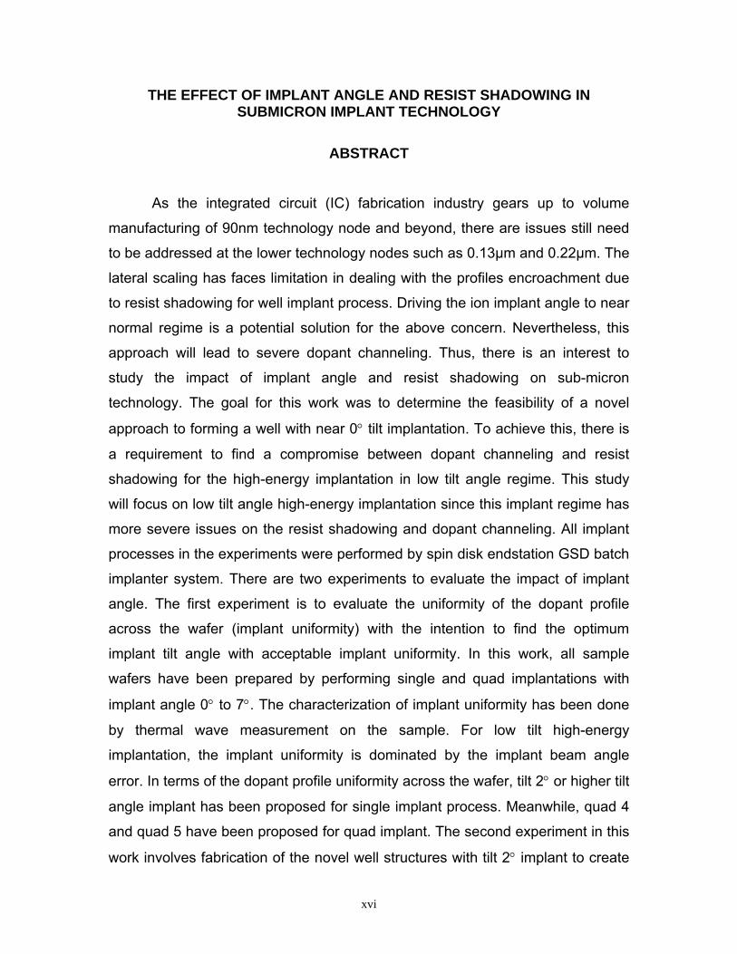
The shadowing creates shadow regions (lateral encroachment) of the well
profile as shown in fig 1.1 [3-6]. This lateral encroachment is relatively larger
compare to the CMOS well for smaller device (see fig 1.1) and creates a barrier for
device miniaturization. By reducing tilt implant angle towards 0°, the interwell
isolation can be improved by reducing the lateral diffusion of the well dopant
profile [7].
Fig 1.1 The encroachment of well due to thick photoresist (PR) shadowing for tilted implant
of different device dimension [3]
Another concern in the junction engineering for well implant is the control of
implant angle [8, 9]. The process control of implant angle highly depends on the ion
beam scanning and wafer holder design of the implanter. For batch processing
implanter where the wafers will put on a spinning disk (the spinning disk implanter
will be reviewed in Chapter 3), the implant beam angle will deviate from the actual
direction due to space charge and cone angle effect [9-15]. Since implant angle will
affect the doping profile, any change in beam angle across the wafer may affect
the implant uniformity. The uniformity of the doping profile across the wafer, as
spatial variation of doping dopant across the wafer [11] is dependent on the implant
angle setting [15]. Thus, proper setting of the implant angle is crucial for best
implant uniformity across the wafer.

3
The issues above mentioned indicate that the implant angle engineering is a
critical part of the junction engineering. Any improvements in the implant angle
control will lead to dopant uniformity improvement, which will result in enhanced
device performance and improved yields.
1.1 Well structure with channeled and dechanneled implant approach
As stated in section 1.0, higher implant angle* for well implants will lead to
severe “mask edge shadowing”. The near 0° tilt well implant has been proposed as
the solution to this issue [7].
It is known that channeling will occur at near 0° tilt angles [7]. Thus,
conventional high tilt angle and high-energy well implantation will create abrupt
doping profile with less dopant channeling. This will result in dechanneled well
structure with a steep retrograde well. The proposed methodology discussed in this
project is to form the well with uniform channeled doping profile and result in
channeled well [16].
(a) (b) Fig 1.2 Retrograde well structure formed by (a) high tilt dechanneled implantation and (b)
channeling implantation [16]
Fig 1.2(a) shows a conventional well structure with dechanneled profiles
under STI (shallow trench isolation) and active region by tilting the implant angle * High tilt angle is defined as the tilt angle higher than tilt 3° in this thesis

4
high enough to non-channeled regime. The proposed well structure in fig 1.2(b)
requires 0° or near 0° implant to reduce the impact of resist shadowing. Fig 1.2 (b)
shows the channeled profiles under active region and dechanneled profiles under
STI. Low tilt implant in the high channel regime will create channeled doping
profiles in the active region. Under the STI region, the implanted ions show
dechanneled behavior because the STI oxide acts as the screen oxide to scatter
the implanted ions [16].
In some cases, well implant with high tilt angle is performed in quad mode,
which is known as quad implant process.
1.2 Formation of the well structure by quad implant
Quad implant process is a chain of four implants, each with one quarter of
the dose. The implant angles will be at the same tilt, but 90° apart in twist. The
quad implant angle for the disk implanter NV-GSD200 HE implanter (the model of
implanter used in this work) will consist of (α, β), (-β, α), (β, -α) and (-α, -β) all with
quarter of total dosage, where α and β are angles in degree (see table 1.1).
Table 1.1 Quad implantation sequences [17].
In this thesis, quad 1 will consist of 4 implant steps with angle (1,0), (0,1), (-
1,0) and (0, -1). Meanwhile, quad 7 will consist of 4 implant steps with angle (7,0),
(0,7), (-7,0) and (0, -7).
The quad implant can be used to form the symmetrical well of a standard
CMOS as shown by fig 1.3(a) below. The near 0° tilt well implant approach in fig
1.3(b) will form a novel channeled well (see section 1.1) [14].

5
(a) (b)
Fig 1.3 Formation of Nwell by (a) high tilt quad implant process (b) near 0° tilt implant
process
The symmetrical well profiles encroachment of quad implant can solve the
asymmetry of device performance due to photoresist shadowing [14]. However, the
concern of the encroachment of well profile still exists if the quad implant involves
high tilt angle. Thus, there is a requirement to lower the implant tilt angle to reduce
the dopant profiles encroachment.
1.3 Objective
The intention of this work is to study the feasibility of forming a CMOS well
with near 0° tilt high-energy implantation by using batch implanter with spinning
disk endstation design. To achieve this, experiments have been carried out in order
to evaluate the implant uniformity across the wafer for high-energy implant with
different tilt angle and evaluate the device performance for the well with channeled
and dechanneled doping profiles.
The objectives of this work can be summarized as following:
• To find the high-energy implant tilt angle with the optimum dopant profile
uniformity across the wafer

6
• To evaluate the device performance for well implant with near 0° tilt and
high tilt quad implant
• To fabricate a MOSFET with improved interwell isolation performance.
1.4 Thesis Overview
This thesis is divided into 7 chapters. The first chapter is the introduction to
the control of implant angle for high-energy implant. In this chapter, the motivation
and objective of this project are stated.
Chapter 2 is the literature review. The technical challenges and issues on
low tilt angle for high-energy implant application as well as the history of previous
works on the implant angle study are discussed. The implant angle control has
been addressed. Apart from this, the device performance of 0° tilt approach to form
the well is reviewed.
Chapter 3 reviews the fundamental concept of ion implant angle and dopant
channeling. This chapter also discusses the endstation design for spinning disk
implanter, cone angle effect and angle variation arising from it. In addition,
description on the implant metrology theory (thermal wave) is reviewed. Then, the
electrical characterization of CMOS well will be stated (test method and test
structures for interwell isolation, intrawell isolation, parasitic junction capacitance,
and parasitic bipolar beta gain).
Chapter 4 is the experimental setup where the tools such as ion implanter
and the metrology used in this project will be stated. The specifications of the
equipment setup were addressed as well.
Chapter 5 discusses the methodology of the experiment. The design of the
experiments in this work will be shown. The experimental works can be generally

7
divided to thermal wave analysis on bare-wafers for implant profile uniformity
evaluation and the comparison of the device performance for well implant with low
tilt single implant and high tilt quad implant.
The experimental results will be discussed in Chapter 6. The early part of
this chapter will evaluate the implant profile uniformity for different implant angle.
The factor that dominates the implant profile uniformity across the wafer was
stated. Then, the impact on dopant channeling on the CMOS well will be
discussed. Based on the analysis in this chapter, optimum implant angles for well
implant process will be proposed. The device performance for the MOSFETs,
which were fabricated with the implant angle proposed in the first experiment will
be shown as well.
The conclusion and the future work of thesis research are presented in
Chapter 7. Meanwhile, other experimental data can be referred in Appendices.
8
CHAPTER 2 LITERATURE REVIEW
2.0 Introduction This chapter covers the literature review of earlier works done on ion implant
angle and shadowing effect. The chapter is split into three sections. First section
covers the spatial variation in ion implantation from disk implanters. Second section
goes over the impact of tilt angle error on the device performance. The third
section reviews the 0° tilt approach to form the well.
2.1 Review on the spatial variation in ion implantation
As mentioned in chapter1, the spatial variation (non-uniformity) in the well
dopant profiles [10] is the main challenge in implant angle engineering to perform
the near 0° tilt well implant. This non-uniformity may present itself as a tilt, beam
divergence, beam micro non-uniformity, photolithography, or even crystal cut error
[19]. It has been reported that the non-uniformity of high-energy batch implantation
is mainly contributed by the beam angle variation from batch implanter [10].
There are abundant literatures [8,9,11,20 - 22] emphasizing the requirement
of implant angle control of the single wafer processing implant. This papers
reported the limitation of the batch processing implanter to produce the uniform
channeled doping profiles in the low tilt implant regime due to their beam angle
accuracy from cone angle effect from the spinning disk endstation. Even though
the batch implantation (with spinning disk endstation) has disadvantage on the
accuracy of the beam angle, the dual tilt spinning disk endstation of batch
implanter allows a fast adjustment of wafer tilt and twist angles and provides a high
throughput for a quad implantation as is proposed by Axcelis technology.
9
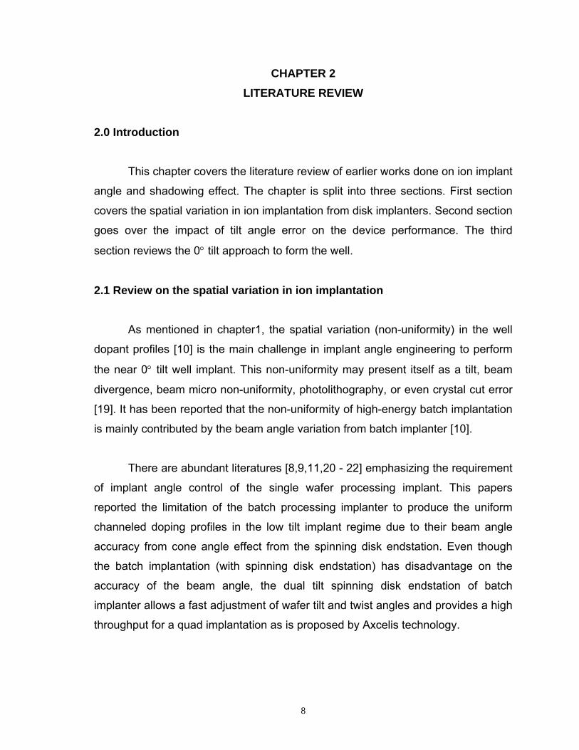
Studies have been done to reduce the spatial variation dopant profile
[8,9,17]. The implant angle study by Serguei Kondratenko [17] on low energy
Boron quad implant has reported that tilt 7° twist 45° ((α,β) = (4.95°, 4.95°)) can
reduce the spatial variation and dopant channeling. This implant condition has
resulted in a relatively high sheet resistance (Rs), indication of reduced channeling,
and low standard deviation of Rs which is an indication of reduced spatial variation
as shown in fig 2.1.
Fig 2.1 Rs average and standard deviation as a function of implantation twist angle for 5°
and 7° tilt angle. Quad implant process: B+, 5 keV, 4x10¹³ ions/cm2 [17].
It has also been reported that the wafer cut error will contribute to the
incident beam angle error [10], which is tabulated in table 2.1 (see fig 2.2 for the
variation of doping profiles between different substrate batches). The wafer cut
error only lead to the wafer-to-wafer doping profiles variation and not the main root
cause of the spatial variation across wafer.

10
Table 2.1 Wafer cut offsets form <100> plane [10].
Fig 2.2 Doping profile for substrate lot number #1 to #5 in Table 2.1 [10].
2.2 Review on the impact of implant tilt angle
The impact of the small angle change on the shape of doping profiles has
been reported [8]. The sensitivity of the profile shape to angles will rise with
increasing ion energy [23]. Apart from this, comprehensive SIMS analyses also
been performed on the low tilt high-energy implant regime [24]. Based on the SIMS
analyses [24], there was a significant variation of the profile shape for the implant
tilt lower than 1° (see fig 2.3(a) and fig 2.3(b)).

11
Fig 2.3 a) SIMS depth profiles for B++, 540keV, 2X1013cm-2 at various tilt angles [8].
Fig 2.3 b) SIMS measurements and simulation results for P, 800keV, 3X10¹³ atoms/cm2,
0° twist with tilts at 0°, 0.2°, 0.4°, 0.6°, 0.8° and 1.3°. SIMS measurements were performed
at the wafer centers. For 0° and 0.8° tilt, SIMS measurements were performed at wafer left
and right positions from the 10mm wafer edges and consistent SIMS profiles across the
wafers were obtained. Crystal-TRIM simulation result at 0° tilt is shown [24]

12
The well profiles (see fig 2.4(a)-(b)) has also been simulated [7] to study
their impact on Vth and N+ to Nwell isolation by using TSUPREMIV. For processes
with 0° tilt well implants, beam angle variations <1.0° significantly alter the shape of
typical n-well and p-well doping profiles (see fig 2.4(a)-(b)), Vth (see fig 2.5(a)) and
interwell isolation performance (see fig 2.5(b)) compare to quad 3 well implants.
Fig 2.4 a) Simulated net doping profiles n-well [7].
Fig 2.4 b) Simulated net doping profiles p-well [7].

13
(a) (b)
Fig 2.5 (a) Change in Vth for PFET and NFET as a function of implant angle error. (b) Isolation robustness for all implant and photoresist conditions investigated [7].
The tilt angle variation of the high tilt halo implant also induces significant
impact on the device performance [25, 26]. The angle error [27] on the halo
implant may induce significant effect on the threshold voltage (Vth) (see fig 2.6(a)),
drive current (Id) (see fig 2.6(b)) and off state current (Ioff) (see fig 2.6 c)) for
0.14µm CMOS transistor.
Fig. 2.6 (a) Normalized Vth, (b) normalized Ion, and (c) normalized Ioff box plots for devices as a function of halo implant tilt angle. Normalization is with respect to mean values obtained from the nominal cell (0° tilt angle offset) [27].
Then, the dependence of depth profile and threshold voltage on tilt and twist
angle has been investigated with a resolution of 0.05° using a stencil mask ion
implanter that has less than 0.1° parallelism of ion beam [28]. By controlling beam
parallelism to less than 0.1°, the deviation due to the channeling phenomena
14
should be negligible (refer to fig 2.7 for the impact of implant angle on the threshold
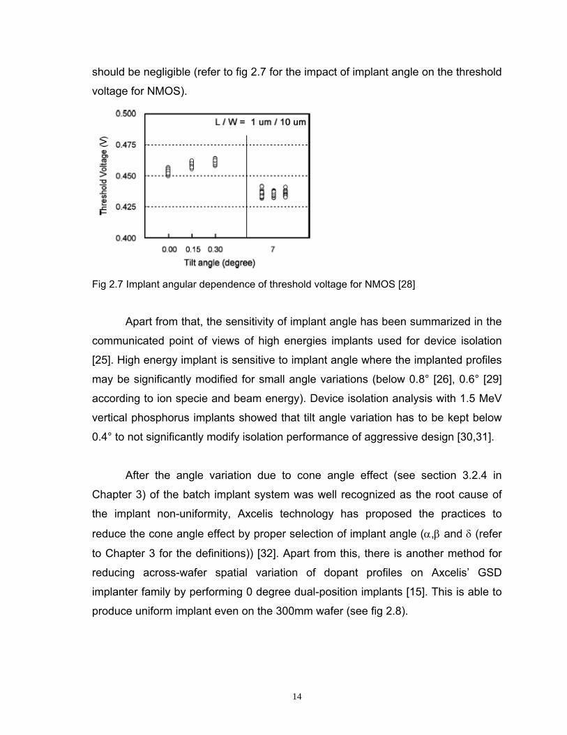
voltage for NMOS).
Fig 2.7 Implant angular dependence of threshold voltage for NMOS [28]
Apart from that, the sensitivity of implant angle has been summarized in the
communicated point of views of high energies implants used for device isolation
[25]. High energy implant is sensitive to implant angle where the implanted profiles
may be significantly modified for small angle variations (below 0.8° [26], 0.6° [29]
according to ion specie and beam energy). Device isolation analysis with 1.5 MeV
vertical phosphorus implants showed that tilt angle variation has to be kept below
0.4° to not significantly modify isolation performance of aggressive design [30,31].
After the angle variation due to cone angle effect (see section 3.2.4 in
Chapter 3) of the batch implant system was well recognized as the root cause of
the implant non-uniformity, Axcelis technology has proposed the practices to
reduce the cone angle effect by proper selection of implant angle (α,β and δ (refer
to Chapter 3 for the definitions)) [32]. Apart from this, there is another method for
reducing across-wafer spatial variation of dopant profiles on Axcelis’ GSD
implanter family by performing 0 degree dual-position implants [15]. This is able to
produce uniform implant even on the 300mm wafer (see fig 2.8).

15
Fig 2.8 SIMS profiles at center, left and right location (Qual-center, Qual-Left and Qual-
Right) of a wafer for P, 400keV, 1.5x10¹³ ions/cm2 implanted using a dual setting of (α, β)
of (0°, 1°) + (0°, -1°) on an HE 300mm implanter [15].
2.3 Review on the CMOS device performance of 0° tilt approach to form
retrograde well
Simulation study has been performed on the 0° tilt approach to form the
retrograde well [32]. Based on the simulation, 0° tilt implantation is estimated to
improve inter-well isolation by 0.2µm compared with 7° tilted implantation for 0.1µm
retrograde well process. This retrograde well technology is indispensable for inter-
well isolation in 0.1µm node. The technical challenge of performing near 0° tilt well
implant approach by using batch implanter series has been reported due to their
relatively poor dopant profiles uniformity within the wafer (see fig 2.9 for the implant
uniformity of batch implantation with different tilt angle) [32].
16
Fig 2.9 Implant uniformity (in standard deviation of Rs) within 8-inch Wafer (after 900°C
annealing) for (a) B+, 200keV (b) P+, 400keV [32].
Another work that studied the device performance on the 0° well implant
approach by using parallel beam implanter [16] reported that 0° channeling
implantation with thin screen oxide can reduce both junction capacitance and
junction leakage current without deteriorating a characteristic of MOSFETs. The
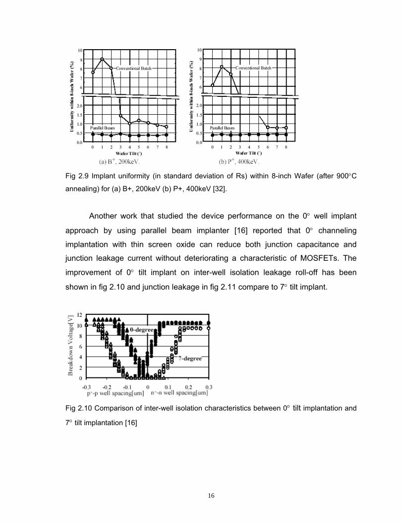
improvement of 0° tilt implant on inter-well isolation leakage roll-off has been
shown in fig 2.10 and junction leakage in fig 2.11 compare to 7° tilt implant.
Fig 2.10 Comparison of inter-well isolation characteristics between 0° tilt implantation and
7° tilt implantation [16]

17
Fig 2.11 A ratio of junction leakage current at |Vd|=4V of 0° tilt implantation to that of 7° tilt
implantation [16].
As reviewed in this chapter, extensive study has been carried out on the
near 0° tilt well implant by using single wafer processing implanter with parallel
beam control system. However, no study has been reported on the capability of
batch implanting process to form the well with near 0° tilt implant approach.
This work will focus on the study for the spatial variation of well implant
process by the high-energy batch implanter. Subsequently, the device performance
of the 0.13µm CMOS well with quad well implant and near 0° tilt well implant
approaches were studied.

18
CHAPTER 3 THEORY
3.0 Introduction
This chapter is divided into four sections, which are theory of ion implant
process, theory of ion implanter, theory of ion implant metrology and theory of
device characterization. Theory of ion implant process covers ion stopping theory
and channeling effect in ion implantation. Then, the fundamental of implanter,
endstation design of spinning disk batch implanter and the cone angle effect in
batch implanter are reviewed in the theory of ion implanter. The theory of ion
implant metrology reviews the metrology to determine the spatial variation of
dopant profiles. At the end of this chapter, the electrical characterizations of the
isolation performance of the CMOS well are reviewed in the theory of device
characterization.
3.1 Theory of ion implant process
3.1.1 Projectile and range theory (Ion stopping theory)
When an energetic ion moves through a solid, the kinetic energy of the ion
is transferred to the lattice through the columbic interaction in nuclear collision with
the lattice nuclei and with the electron around the lattice atoms [36]. The energy
loss per unit length due to nuclear collision is called the nuclear stopping power
Sn(E), and the electronic stopping power Se(E) for electrons. The total distance of
ion traveled in target is the range. The penetration depth of the implanted ion along
the implantation direction is known as the projected range (Rp) as shown in fig 3.1
below.

19
Fig 3.1 Description of ion range R and projected range Rp.
The rate of energy loss can be expressed by equation 3.0 as following [1]
)]()([ ESESNdxdE
en +=− (3.0)
where,
E = energy of the ion at a point x along its path,
N = atom density
The negative sign means that the energy decreases with depth due to the
collision and the columbic interaction. The range can be obtained by integrating
equation 3.0 with respect to energy as expressed by equation 3.1 [1]
∫∫ +==
0
00 )()(1 E
en
R
ESESdE
NdxR (3.1)
However, the actual implanted dopant depth, R will not be exactly as
predicted by equation 3.1 but will be distributed statistically as the doping profiles in
fig 3.2 below.

20
Fig 3.2 Depth profile for 3 MeV Phosphorous [14]
The dopant distribution (doping profiles) can be represented by Pearson IV
distribution with four moments (parameters to represent the distribution of the data
points in statistic) of projected range (Rp), straggle (σ), skewness and kurtosis.
Generally, the doping profiles can be obtained by destructive analytical
measurement such as secondary ion mass spectroscopy (SIMS) and spreading
resistance analysis (SRA). Alternatively, simulation can be done to obtain the
doping profile by using different methods such as binary collision approximation
(BCA) and molecular dynamic (MD) [37]. The example of simulation programs
available has been shown as following in Table 3.1.
Table 3.1 Illustrate the example of simulation programs
Simulator Author Technique Material
TRIM/SRIM Ziegler BCA Amorphous
SUPREM IV Boltzman Amorphous
CRYTAL-TRIM Posselt BCA Crystalline/Amorphous
MARLOWE Robinson BCA Crystalline/Amorphous
UT-MARLOWE Tasch BCA Crystalline/Amorphous
UVA-MARLOWE Arias BCA Crystalline/Amorphous
REED Cai MD Crystalline
MDRANGE Nordlund MD Crystalline

21
There are numerous ion implant simulation programs with different
accuracies based on the model (see table 3.1). The SRIM simulation [38] will be
used to simulate the as implanted doping profile (without annealing) in the
discussion in Chapter 6.
3.1.2 Monte-Carlo based SRIM
Stopping and Range of Ion in Matter (SRIM) simulation is based on Monte-
Carlo calculation to simulate the implanted profiles. The basic concept of Monte-
Carlo calculation is the simulation of the history of a projectile through its
successive collisions with target atoms. The result is based upon the summation of
these scattering events occurring along a large number of simulated particle
trajectories within the target. The particle with a given energy, position, and
direction, is assumed to change direction due to binary nuclear collisions and to
move in straight paths between collisions. The doping profile by SRIM simulation is
shown in fig 3.3.
Fig 3.3 Doping profile by using SRIM simulation [38].
22
SRIM simulation able to predict the projected range and peak concentration
of as-implant profile (implant dopant without annealing) with high accuracy.
However, the limitation of this program is that the target material is assumed as
amorphous, which results in the less effectiveness to predict the ”channeling
effects” usually observed in crystalline substrates.
3.1.3 Ion implant process
Ion implantation has the advantages over more simple techniques such as
driven-in diffusion because of the ability to introduce nearly any kind dopant into
the substrate with precise control of the dopant location and the ability to predict
the dopant location as well as the distribution.
The implanted dose (Φ in cm-2) is precisely controlled by beam current (I in
ampere), and implantation duration (t in second). The implant dosage will
determine the total doping concentration in the implant process. Apart from this,
the energy of implanted dopant can be controlled to determine the range of the
implanted dopant.
Based on the application of implant process, there will be different criteria
for implant conditions such as implant energy, angle and dose. There are different
type of implanters, such as high-current (HC), medium current (MC), ultra low
energy (ULE) and high-energy (HE) implanter designed to achieve desired implant
energy and beam current.
The formation of the source/drain and source/drain extension structure (see
fig 3.4 and fig 3.5) will involve low energy implant process with high dose. This kind
of implant application requires implanter with low energy and high current
capabilities. Other cases like threshold voltage adjust implant (Vt implant) and

23
punchthrough stop implant were generally implanted with medium current
implanter on account of their implant depth and dosage. High-energy implant is
well recognized for p-well, n-well, retrograde p-well and retrograde n-well implant
applications in order to place the dopant in the deep region.
Fig 3.4 Dose and energy requirement of ion implant process depending on the
implantation application [34].
Fig 3.5 The standard CMOS structure [35]

24
In this work, the implant angle and photoresist shadowing study involves the
high-energy implant with the implant depth of 4000Å to 7000Å. This implant
process is well recognized as the well application implant and will be performed by
using NV-GSD200 HE batch implanter.
3.1.4 Ion implant angle
In ion implant process, the direction of incident beam can be defined by tilt
(θ) and twist (Φ) as shown in the fig 3.6(a) below. Tilt (θ) is defined as the angle
between the ion beam and the normal to the wafer surface. Meanwhile, twist (Φ)
can be defined as the azimuthal angle between the projection of the ion beam on
the wafer surface and the [011] crystallographic direction (the direction from the
center of the wafer to the wafer notch) [32].
(a) (b)
Fig 3.6 (a) Definition of tilt (θ) and twist (Φ) (b) wafer orientation for <100> wafer [2]
Changing the tilt angle for the implant process can be analogy as placing
the dopant at different wafer orientation. In semiconductor industry, the production
wafer for integrated circuit fabrication will use silicon substrate in the (100)
orientation as shown in fig 3.7. Thus, tilt 0° implant will be referring to implant the
dopant into silicon wafer with (100) orientation and tilting the implant angle will be
referred from this orientation as well.