the effect of doping thiourea in cdo thin films for
TRANSCRIPT

The Effect of Doping Thiourea In CdO Thin Films ForElectronic ApplicationsMurat Soylu ( [email protected] )
Bingol University: Bingol Universitesi https://orcid.org/0000-0002-1913-9833
Research Article
Keywords: CdO, Thiourea doping, heterojunction
Posted Date: July 13th, 2021
DOI: https://doi.org/10.21203/rs.3.rs-688896/v1
License: This work is licensed under a Creative Commons Attribution 4.0 International License. Read Full License
1
The effect of doping Thiourea in CdO thin films for
electronic applications
M. Soylu*
Department of Physics, Faculty of Sciences and Arts, Bingol University, Bingol, Turkey
Abstract
Cadmium oxide (CdO) and Thiourea (Th) doped CdO thin films were deposited on soda lime
glass (SLG) and crystalline p-type Si (100) substrates for various Th doping concentrations
(0.3, 0.5, 0.7 at.%) using spin coating method. Some structural parameters such as the
crystallite size, lattice constant, dislocation density (δ) and strain in the films were obtained
from XRD analysis in which the polycrystalline structure with cubic nature and (111)
prefential orientation was confirmed. CdO thin film has not shown any change in crystal
phase after Th doping. The optical study emerged that the Th doping caused important
changes in the transmittance, absorbance and reflectance spectra. A maximum optical
transmittance (above 80%) have been obtained for 0.3% Th doped CdO thin films. Th doped
CdO/p-Si heterojunctions exhibited low rectifying character and were not found to be the light
sensitive.
Keywords: CdO, Thiourea doping, heterojunction
*Corresponding author: Department of Physics, Faculty of Sciences and Arts, Bingol University,
Bingol, Turkey e-mail address: [email protected] ; [email protected] (M. Soylu)

2
1. Introduction
Semiconducting nanostructures are of great importance for device technology due to
unique optical and electrical properties. The efforts have been made for the development of
semiconductors for years. Compound semiconductors that are made from two or more
elements have widespread applications. Transparent conducting oxides (TCOs) are an
example of compound semiconductors [1-3]. TCOs have attracted a great attention of
scientists in optoelectronic applications such as solar cells, phototransistors, flat panel field
and manufacturing of gas-sensing.
CdO films are characterized by transparency in near-infrared (NIR) spectral analysis [4-6].
CdO shows n-type semiconductor property, which might be due to oxygen (O) vacancies (VO)
and Cd interstitials (Cdi). CdO exhibits some features as the moderate indirect (1.98 eV) band
gap, low resistivity of 10-2–10-3 Ω cm, relatively high electrical conductivity (102–103 S/cm)
and rock salt crystal structure. [7]. This material stands out with synthesis methods as sol–gel-
spin coating [8], successive ionic layer adsorption and reaction (SILAR) [9], spray pyrolysis
[10], vacuum evaporation [11], radio frequency magnetron sputtering [12], chemical bath
deposition [13]. Sol-gel method suggests some attractive features, such as lowcost equipment,
easy control of growth and amenability to large area coverage. Relatively small band gap of
CdO is one of its disadvantages for the photovoltaic applications. CdO acts like a degenerate
semiconductor (close to metal) at high level of doping. The absorption edge can be shifted by
free carriers in the conduction band (Burstein–Moss efect) [14,15]. Ganesh et al. [16]
prepared Nitrogen (N) doped (1-20%) cadmium oxide thin films on the glass substrates in
their work using sol-gel spin coating method. They obtained the optical direct and indirect
band gaps varying with the doping concentration in the range of 3.92-3.98 eV and 3.24-3.49
eV, respectively. In addition, several research groups reported that increasing doping
concentrations decreased the band gap. Kabir et al. [17] carried out a work on strontium (Sr)
3
doped cadmium oxide (CdO) thin films by using spray pyrolysis technique. It is seen that the
band gap of CdO decreases from 2.67 to 2.49 eV, as Sr quantity in CdO increases (1%, 2%,
3% to 4%).
Generally, there are studies in which single or co-doping of elements to TCOs are made in
literature. But, Cho et al. [18] reported the synthesis of ZnO nanostructures by organosulfur
compound thiourea (SC(NH2)2) with sulfur (S). Scanning electron microscopy (SEM) images
show that the shape of the nanostructure changes with the concentration of thiourea. Density
functional theory (DFT) suggests that sulfur atoms prefer to be found at the hexagonal
vertices of ZnO, leading to a change in charge distribution. From the photoluminescence (PL)
spectra, the emission peak shows a slight blue-shift with increasing the concentration of
thiourea, visible light emission where there is a concept of interest in visible light emitting
device applications. Blue-shifted or enhancement visible light emission is ascribed to the
change of S doping in ZnO nanostructures [19,20].
Recently, intense attention has been paid to understanding TCO-charge transport. Metallic
oxide films might show rectifying property while brought into contact with a semiconductor.
Therefore, CdO thin films as an electron transport layer are used at p–n heterojunctions,
depositing on p-type silicon (Si) semiconductor. Research should include the mechanisms that
are needed to explain the charge transport for construction of optoelectronic nanotechnology.
CdO thin films grown on p-Si substrates were studied, forming p–n heterojunctions [21-23].
To the best of our knowledge, no an experimental investigation has been performed on
Thiourea (Th) doped cadmium oxide (CdO) thin films.
In the present work, we report the growth of Th doped CdO on Si and glass substrates by sol-
gel method. Th doped CdO thin film microstructure, crystal structure, optical and electrical
properties are examined in detail with increasing doping level.

4
2. Experimental Details
To prepare CdO thin films, 2-methoxyethanol (C3H8O2), monoethanolamine (MEA)
(C2H7NO), Cadmium acetate dihydrate (CAD) (Cd(CH3COO)2.2H2O) were used. The
materials (precursor, solvent and stabilizer) were adjusted so that the molarity of the solution
was 0.5 molar. CAD was dissolved in 2-methoxyethanol (C3H8O2). The explanation of all the
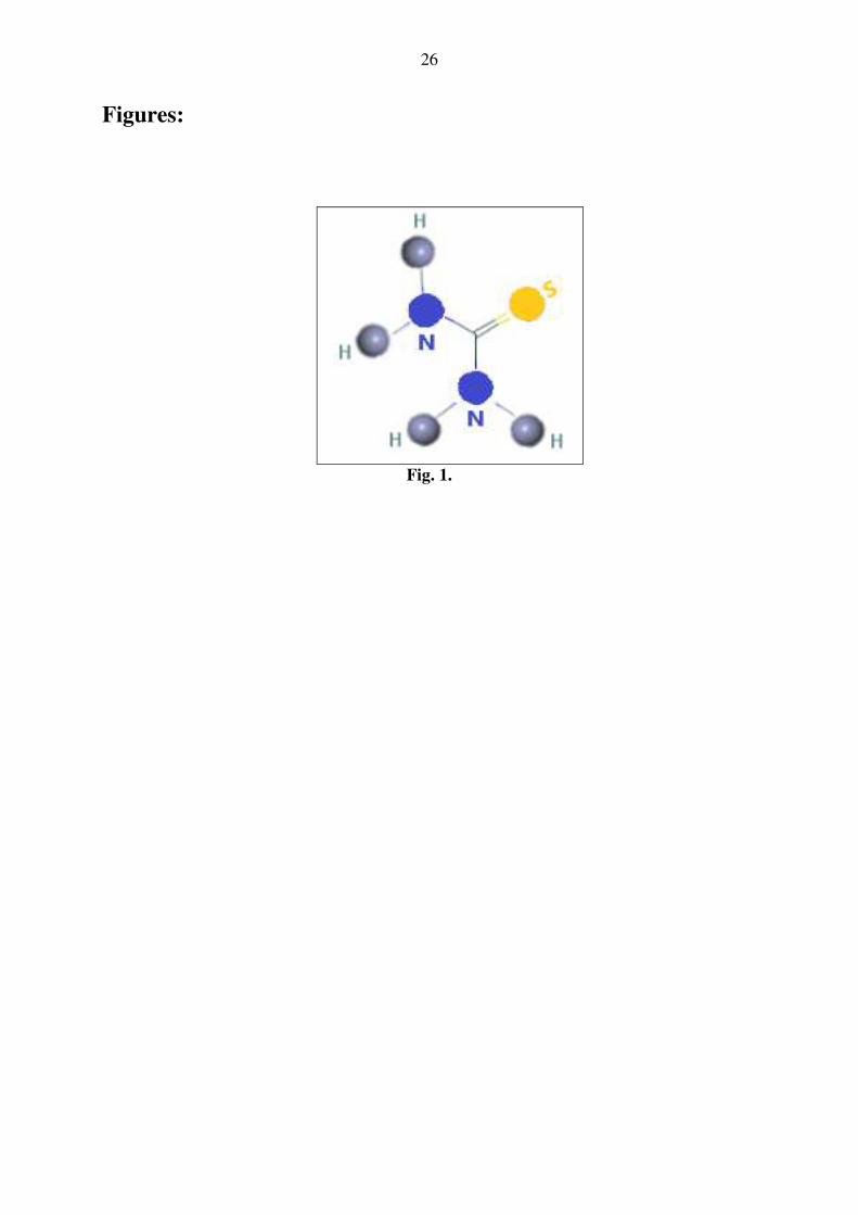
processing operations is presented in our previous work [24]. Molecular Formula of Thiourea
is given as CH4N2S or H2NCSNH2. Fig. 1 shows a schematic representation of Thiourea. In
fact, by adding Thiourea (Th), sulfur is added to CdO. CdO thin films with different
proportions of Thiourea (Th0.03Cd0.99O, Th0.05Cd0.95O, Th0.07Cd0.93) were prepared. The
solutions were coated on the ultrasonically cleaned soda–lime glass substrates with spin
coating method. The spin speed was adjusted at 1500 rpm at a fixed spinning time of 60 s.
Three samples obtained were thermally annealed at 1h in furnace, when the temperature
reached 400 °C. p-Si (100) substrate was used to obtain the heterojunction. Chemically
cleaned samples were exposed to pure nitrogen gas. The front face of p-type Si substrates was
coated with Th doped CdO and the annealing process was applied. Coating/annealing
parameters of soda–lime glass substrates were continued and then, to obtain Al/Th:CdO/p-Si
device structures, circular shaped Al contact was made on Th doped CdO thin films. The
atomic force microscopy (AFM) was used to measure the surface morphology of the CdO thin
films. Crystallographic data of the CdO thin films are routinely characterized using x-ray
diffraction (XRD, Rigaku) with Cu Kα radiation. The transmittance, absorbance and
reflectance data were were obtained by the aid of UV-vis spectrophotometer (Shimadzu UV-
VISNIR 3600). The current-tension (I-V) relationship for Th:CdO/p-Si heterojunctions was
supplied by a Keithley 2400 voltage source. Raman spectroscopy was evaluated to obtain the
information about molecular vibrations.
5
3. Results and Discussion
3.1. Morphological, Structural and Optical Characteristics
Fig. 2a-c shows the AFM images of CdO thin films; 40x40 µm, 5x5 µm and three-
dimensional (3D) for 0.3%, 0.5% and 0.7%, respectively. It appears that nanoclusters are
formed in all three of the samples, but they do not show a homogeneous distribution on the
surface. The surface distribution observed along the red line is also seen in the images of
40x40 µm. The roughness of the surface is in the order of nm for 0.5% Th doped CdO
samples, while for CdO with 0.3% and 0.7% Th doping it is in the order of microns. Also, the
Figs show statistics of the surfaces such as roughness average of the surface (Ra), peak to
valley roughness (Rpv), root mean square roughness (Rq) and average maximum height (Rz).
Morover, Skewness (Rsk) and Kurtosis (Rku) are related to the asymmetry and the peakedness
according to the the mean line at the profile, respectively. The effect of doping Th is seen
along the parameters of the surface moprhology.
Fig. 3a-c shows the scanning electron microscope (SEM) images of CdO thin films at
17000 magnification. The images obtained with SEM show that each sample offers a different
surface map. Energy-dispersive X-ray spectroscopy (EDX) data is also provided. The results
include a large number of elements. The presence of unexpected elements other than the Th
doped CdO composite structure is probably due to the glass used as substrate. Thiourea has
the formula SC(NH2)2. It is organosulfur compound and contains sulfur. EDX results confirm
the presence of the element sulfur (S). While sulfur content is not reported in CdO with 0.3%
Th doping, S ratio is specified in CdO thin films with 0.5% and 0.7% Th doping. It is also
noteworthy that the increasing Th ratio is parallel to the S ratio.
Fig. 4 shows X-ray diffraction (XRD) pattern of Th:CdO thin films with various Th
dopant concentrations (0.3%, 0.5%, 0.7%) deposited on the glass substrates. The preferred
plane densities of the films are varied due to the increasing thiourea concentration. CdO thin

6
films show (111) and (200) preferential orientation in the thin film form, which has a cubic
crystal structure. Peaks is in good agreement with the card number of Joint Committee on
Powder Diffraction Standard (JCPDS) JCPDS: 05-0640. The CdO thin film has not shown
any change in crystal phase after Th doping. Other crystalline orientations such as (220) and
(311) have high intensity and well matched compared to literature [25,26]. The shifts change
in the diffraction peaks, when Th is increased into the CdO lattice structure. Peaks appear to
be more dominant at Bragg’s angle (2θ) of 33° to 38°. These are major difraction peaks at
various diffraction angles. The structure is indexed according to the face centred cubic (fcc)
arrangement. Due to the addition, no phases (peaks) are revealed in the 0.5 and 0.7 wt% of Th
doping. No structural deformation happens and all samples keep crystalline solid state. The
peak of the crystalline orientation such as (311) loses dominance in 0.7% Th doped CdO thin
film. It can be noticed that surface texture (orientation) characteristic depends on doping
elements, including the stress, elongation and elasticity.
The texture coefficient (TC(hkl)) value represents the growth surface and is given as follows
[27],
n
hklhkl
hklhkl
hklIIN
IITC
)(0)(
1
)(0)(
)(/
/ (1)
where N represents the diffraction peak number, I(hkl) is the observed relative intensity of the
plane (hkl), Io(hkl) is the standard intensity. The (111) and (200) preferential plane growths
show dominant peak intensity as in earlier reports [28,29]. Table I contains the texture
coefficients for CdO films, depending on the amount of doping Th. Since CdO thin films
include randomly oriented grains, the texture coefficient is important. The texture coefficient
values close to 1 indicate the presence of randomly oriented grains [30]. It is observed that the
7
Th doping changes partially the texture coefficient values. It is seen that the textured CdO
surface is especially dominant along (100) plane. The surface texture of the thin films reflects
the mismatch of grain boundary. This is associated with porosity and plays an important role
in the gas sensing mechanism [31].
The full width at half maximum (FWHM) is used as a tool to evaluate the peak intensity. The
values of FWHM is given in Table I as a function of Th doping. FWHM gets smaller values
for the (111) and (200) planes, which are the dominant peaks, increasing with doping
concentration. The Scherrer equation is given to find the crystal size (D) of the particles [32]:
cos
94.0
FWHM
D (2)
Where. 0.94 correlation coefficient is used. , λ represent the Bragg angle and the incident x-
ray wavelength (1.5406 A°), respectively. Table II shows that the nm-scaled crystal size for
the crystal plane (200) decreases with increasing Th concentration. The observed pattern is
contrary to the previous report on Sr-doped CdO [17]. The decreasing nature of the XRD
peaks with Th is due to the decreasing crystallite size [33]. The change in crystal boundaries
also has an effect on crystal size. In addition, dislocation density (δ) and strain (ε)
(considering the crystallite size along c-axis) are some of other structural parameters, given as
[34].
2
1
D (3)
4
cos (4)

8
The values are given for the crystal plane (200) in Table II. The dislocation density (δ) is in
order of 1014 lines/m2 while it is obtained in 1015 lines/m2 value for spray pyrolized strontium
(Sr) doped cadmium oxide (SCO) thin films in Ref [17]. Both the δ and ε values increase with
increasing Th doping concentration. Small dislocation density is associated with the
crystalline quality or high degree of crystallinity of the film.
The lattice constant (a) for cubic structured CdO is given as [35]:
2
222
2
1
a
lkh
d (5)
The lattice constant values of samples annealed 400 oC for (200) preferential peak are give in
Table II. The values obtained were found very close to the standard lattice constant value of
CdO (4.69 A˚). It can also be deduced from the experimental results that the Th contribution
and its varying amount have an effect on the lattice constant.
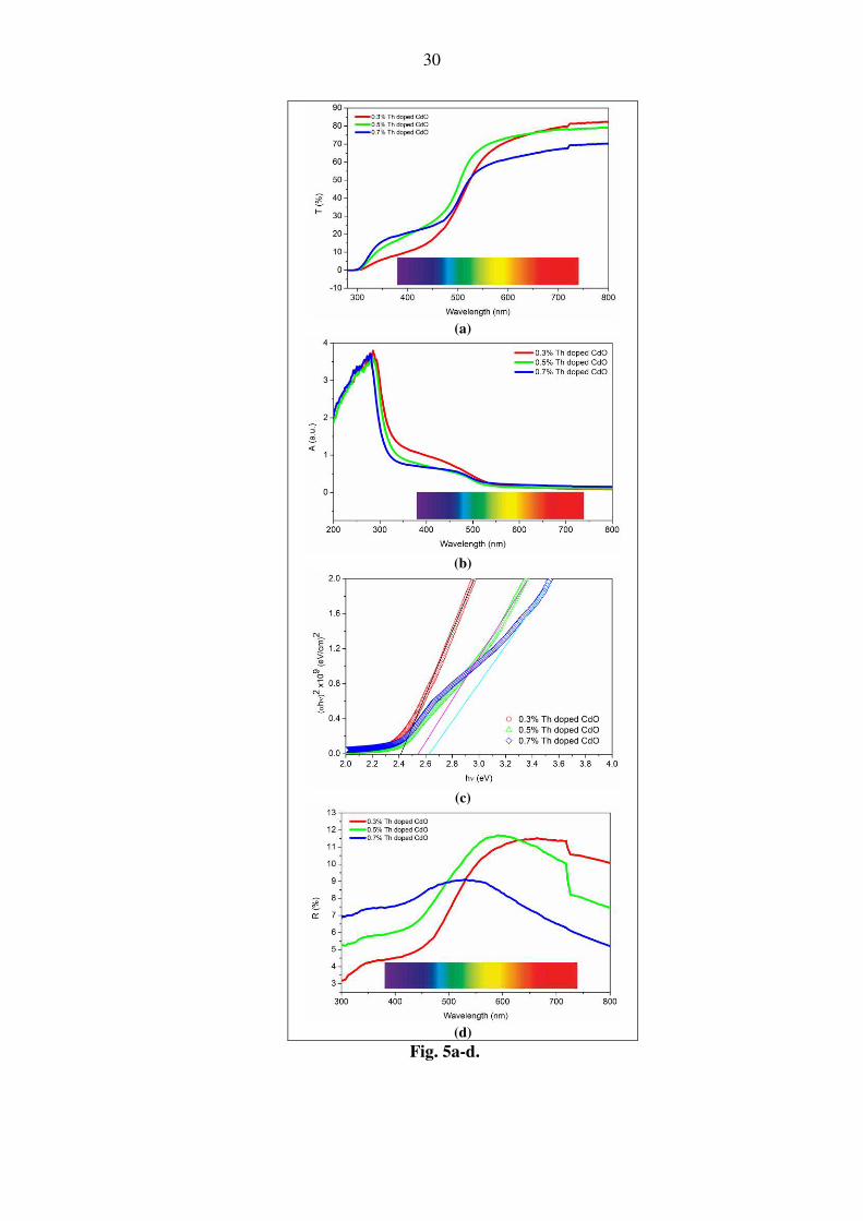
Fig. 5a shows the optical transmittance measurements for 0.3%, 0.5% and 0.7% Th doped
CdO thin films in the wavelength range of 280–800 nm. While the transmittance increases at
about 300 nm, it shows a fluctuating trend, increasing again at around 480 nm with increasing
wavelength. It does not change significantly in longer wavelengths. It is seen that the
transmittance of 0.3% Th doped CdO thin films is lowest in the UV region up to the visible
region limit and the transmittance increases with increasing Th contribution. However, 0.3%
Th CdO thin films show the highest transmittance at long wavelengths with a value above
80%. There are reports in the literature that the transmittance of CdO thin films decreases
with increasing amount of additive element. [36,37]. The effect of S-2 ions, which can replace
the oxygen vacancies or Cd+2 ions, can be considered. It is relevant to state that transmittance
reduction due to increased doping is not related to scattering.
9
Fig. 5b shows the absorption spectra of Th:CdO thin films. It is seen that the absorbance edge
decreases as doping concentration increases. The spectrum shows two different absorption
discontinuities (absorption edge) at about 300 nm and the other at about 500 nm. While the
absorbance is almost constant in the spectrum of visible region, the increase in the UV-region
that starts with a bump turns into a peak as the wavelength decreases. Similar behavior was
also observed in the study examining the optical characteristics of Indium-doped cadmium
oxide thin films prepared by Ganesh et al. [33]. Touch technique can be used to obtain the
optical band gap (Eg) [38]:
n
gop EhBh )( (6)
where absorption coefficient, Bop is a constant coefficient, n is an exponent (index)
associated with the character of the optical transition and h is the photon energy. This index
follows the allowed direct, forbidden direct, allowed indirect, forbidden indirect transition as
1/2, 3/2, 2 and 3, respectively. The value of n is determined as ½ for CdO with direct
transition.
Fig. 5c shows (αhν)2 vs. hν. The value of optical band gap is determined using the
extrapolation of the straight-line portion, corresponding to an approximate accuracy of 0.05
eV (Table II). The obtained bandgap values were found within the standard range of Eg (CdO)
(2.2–2.6 eV) [39,40]. The bandgap of CdO thin film was found to be blue-shifted as Th
incorporation level increases (band-gap widening-BGW). This is attributed to Burstein-Moss
(BM) band gap widening on varying doping of Th from 0.3% to 0.7% [41,42]. The variation
in band gap is due to more O-vacancies resulting from the presence of S content in Th doped
CdO nanostructures. Moss–Burstein BGW could be resulted by the variation of carrier
concentration. The band gap change is phenomenologically affected by the carrier

10
concentration. The band gap for a semiconductor consisting of conduction electrons (Nel) is
given by the following equation [42]:
3/2int
elBGVgg NSEE (7)
The Δ BM
gE is related to the band-gap widening (BGW) [43].
Δ BM
gE =SBGW3/2
elN (8)
3/222
32
e
BGWm
S
(9)
Where γ is equal to evc mm /* as the ratio. *
vcm the reduced effective mass and em is free-
electron mass.
***
111
cvvc mmm (10)
*
cm the conduction band effective mass and *
vm the valence-band. *
vcm is equal to 0.274me
[44]. int
gE as the optoelectronic function is the intrinsic bandgap due to the Cd-Cd and e--
lattice interactions (2.1 eV) [44]. SBGW= 1.348 × 10⁻¹⁸ eVm2 for CdO [45]. The carrier
concentrations for 0.3 and 0.7 wt% of Th doping were estimated to be 1.x1020 and 2.3x10²⁰
cm-3, respectively. It is seen that the carrier concentration increases as Th incorporation
increases.
11
Fig. 5d shows the reflectance characteristics of Th:CdO thin films with various Th dopant
concentrations (0.3%, 0.5%, 0.7%) deposited on the glass substrates. It is seen that the
reflectance increases in the visible region as Th doping concentration increases, but, this
reverses after about 500 nm and it decreases with increasing Th doping concentration in the
IR region.
The exponential edge region is characterized by Urbach-Martienssen rule:
uE
Eexp0 (11)
where Eu and 0 are Urbach energy and a constant, respectively. Fig. 6 shows the plots of
ln(α) vs. photon energy (hν) for CdO thin films with Th (0.3%, 0.5%, 0.7%). The obtained
values are given in Table II. The absorption is due to localized-to-extended-states transitions
in the exponential tail. Urbach energy decreases as Th-content in CdO thin films increases,
and then it increases.
Fig. 7a shows the variation of absorption index or extinction coefficient (k) vs wavelength (λ)
for Th doped CdO thin films. The absorption index is given as following relation:
4
k (12)
As it is seen, the absorption index (extinction coefficient) shows a similar character to the
absorption plot. The absorption index also changes depending on Th doping concentration.
Fig. 7b shows the plots of refractive index (n) vs wavelength (λ) for Th doped CdO thin films.
The exciton coefficient (k) constitutes the imaginary part of the complex refractive index (n):
12
)()()(* iknn (13)
22
22
1
1
kn
knR
(14)
2
21
4
1
1k
R
R
R
Rn
(15)
The refractive index also behaves like reflectance curves and the characteristics change
depending on the concentration. Morover, the refractive index first increases and then
decreases with increasing wavelength. In particular, the region of reduction is known as
normal dispersion and the region of increase as abnormal dispersion region [46]. Refractive
index values of 1.90, 1.74 and 1.60 (0.3, 0.5, 0.7 at.%) at 600 nm are smaller than the values
obtained for In:CdO samples [47]. The changing polarization after reflection and the change
in thickness of the doped films have an effect on the refractive index.
The dispersion is given considering the single oscillator model [48]:
22
0
02 1hE
EEn d
(16)
where Ed is the dispersion energy due to oscillator and represents to the band-to-band
electronic transitions, E0 is the oscillator's energy. The variation of 1/(n2-1) vs. (hν)2 for the
Th:CdO thin films is given in Fig. 8. The values of E0 and Ed are determined from the region
of straight line. As seen in Table II, the dispersion energy and excitation values of the CdO
thin films change with the doping of Th, but, do not show a certain trend. A similar work was
13
made for Boron doped CdO thin films. It was found a relation for the dispersion energy with
doping of Boron [49].
Also, the static refractive index (n0) can be found as the Ed to E0 ratio (Ed/E0) and is given as
follows:
0
0 1E
En d (17)
The values of static refractive index are were found to be 1.63 and 1.54 and 1.46 (0.3, 0.5, 0.7
at.%), respectively. Also, the static dielectric constant can be determined by expressing
εs=n2(0).
Two components, surface and bulk energy change through the dielectric as the total power
loss. Dielectric materials include a dissipation factor (tanδ), which is characterized by the real
(ε1) and imaginary (ε2) parts dependent complex dielectric constant (ε) [50]:
1
2tan (18)
Dielectric with low dissipation factor is required to minimize power losses for high energy
efficiency. Fig. 9 shows the variation of tanδ vs. λ. The dissipation factor decreases as the
doping Th increases.
Bulk and surface energy loss functions (BELF and SELF) are derived by [51]:
2
2
2
1
2
*
1Im
(19)
14
2
2
2
1
2
*11
1Im
(20)
Fig. 10a,b shows the variation of the BELF and SELF vs. h . The probability of electrons to
be excited in bulk and surface is characterized in REELS analysis. The bulk energy loss takes
smaller values than the surface energy loss. It is seen that the energy losses decrease with
increasing Th concentration.
Analysis of the vibration modes is associated with transport properties and phase orientation.
Fig. 11 shows the Raman spectra of CdO thin films. Data with backscattering geometry
includes the incidence of wavelength 532 nm. Raman spectroscopy was activated into the
range of 100 to 4000 wave number. Location and shape of peaks are almost unchanged for
three samples, while peak maxima increase with increasing Th. Weak peak is observed at 385
cm-1. The major Raman peaks correspond to transverse optical (TO) and longitudinal optical
(LO) modes of CdO within the range of 291 to 1000 wave number [51,52]. More intense band
is presented at ~1381 cm-1. Morover, the peaks are centered at 1850 cm-1 and 3269 cm-1,
respectively. Peaks appear to be centered at larger wavelengths compared to the literature [53-
55]. Additional peaks are might be related to the vibration modes, which can be attributed to
the internal stress due to Th and surface influence.
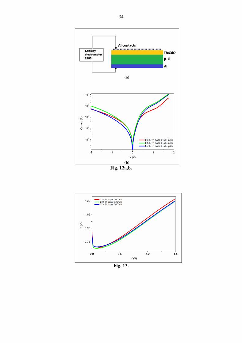
3.2. Current-Voltage (I–V) Characteristics of Th:CdO/p-Si Heterojunction Diodes
Fig. 12a shows the schematic configuration of Th:CdO/p-Si heterojuction. A voltage of ±2 V
was applied to the heterojuction structure. Fig. 12b shows the current-voltage (I-V)
characteristics obtained as a result of the applied voltage. As it is seen, the heterojunction
exhibits rectifying property, including a low rectification ratio in dark condition. The
rectifying nature increases with increasing Th content in CdO. It is thought that there is a
barrier between CdO and p-Si in junction. CdO is considered to have the appropriate Fermi

15
level with p-Si. It introduces a relevant layer for charge carrier transport. No a saturation is
observed in the reverse saturation current. Th:CdO/p-Si diodes do not exhibit a photovoltaic
response to the illumination.
The conduction mechanism of the heterojunction is described by thermionic emission theory
(TET) [56]:
kT
AJRVq
nkT
AJRVqJJ ss )(
exp1)(
exp0 (21)
where, A, A*, k, q, n, T and Rs have well-recognized meanings as characterized in our previous
work [57]. V –JRsA is electrical potential loss across the heterojunction (voltage drop). J0 is
the saturation current density and given by below equation:
kT
qTAJ bexp2*
0 (22)
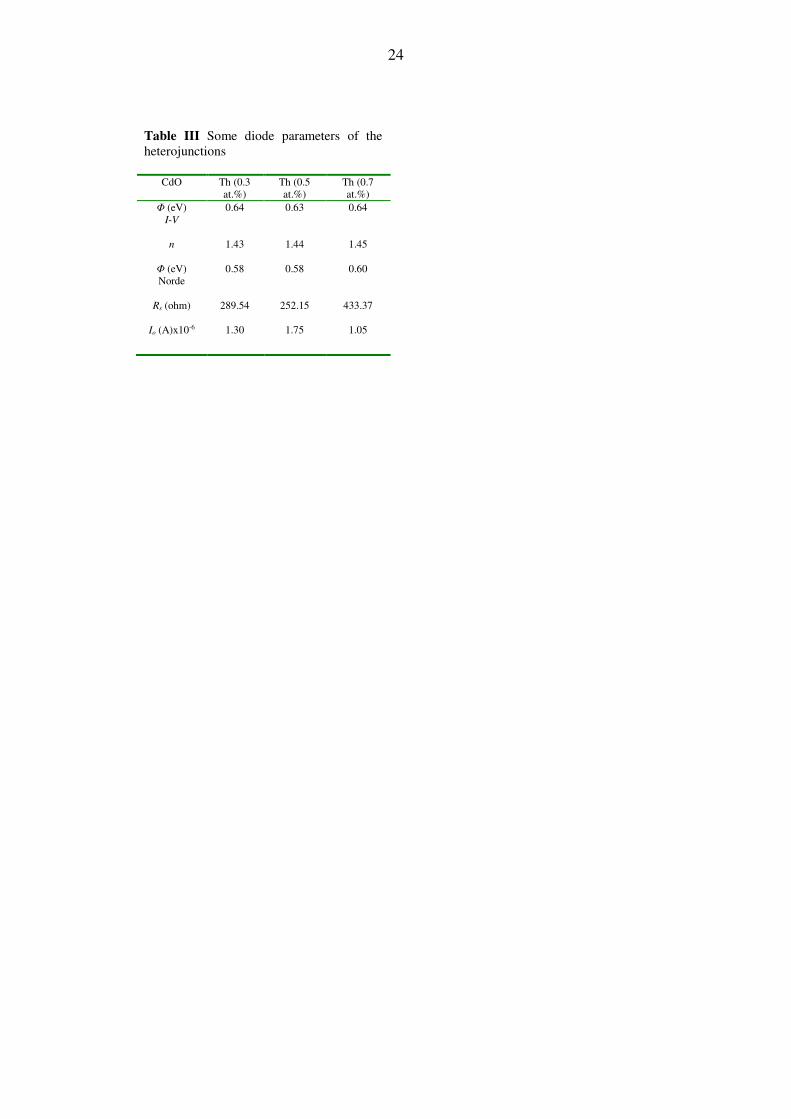
The values of Io for Th doped CdO/p-Si heterojunction diodes are in order of 10-6 A (Table
III), which is initially decreased, then increased with increasing Th doping. The saturation
current flow of the diode seems to vary by Th doping. The barrier height ( b , BH) and
ideality factor (n) are expressed by below equations:
0
2*
lnJ
TA
q
kTb (23)

16
)ln( Jd
dV
kT
qn (24)
The b and n are found from the intercept and the slope of the straight-line region of the log I
vs. V plot, respectively. The values of b were determined to be 0.64 eV, 0.63 eV and 0.64 eV
for Si diodes based on Th:CdO thin films with Th doping (0.3%, 0.5%, 0.7%), respectively, in
dark conditions. Also, it is seen that the ideality factor increases as Th doping increases. The
ideal factor (>1) is attributed to the presence of other current transport mechanisms [58]. The
determined values were obtained from a specific (linear) region of the forward bias I-V
curves. However, Norde proposed a method that allows to find diode parameters from data
that takes into account whole forward I-V data [59]:
2*
0 )()(
TAA
VI
q
kTVVF
(25)
where is a dimensionless quantity. The Norde function, which allows to find the b and
series resistance (Rs) is rewritten as follows:
q
kTVVFb
0
0)( (26)
0
)(
qI
nkTRs
(27)
17
Fig. 13 shows the F(V) vs. V curves. Results are determined by using the points corresponding
to the minimum of plot and given in Table III. The Rs value is high for Al/p-Si heterojunction
with 0.7% Th:CdO thin film layer.
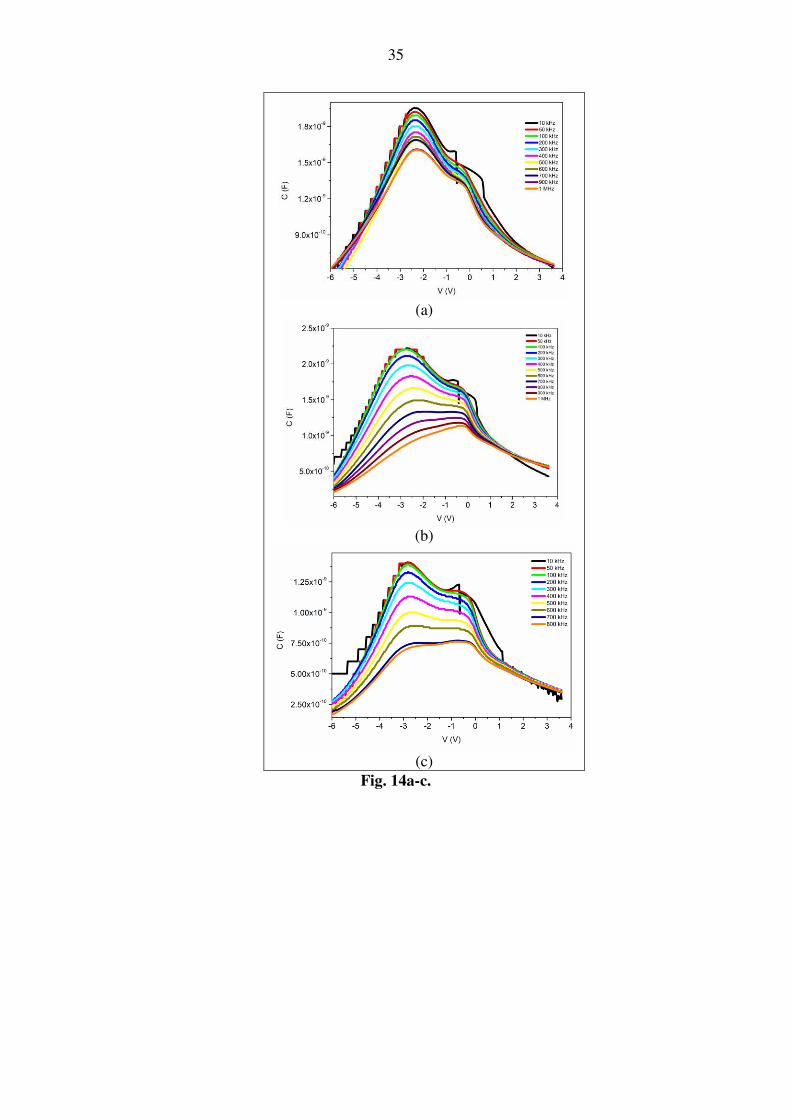
In the forward bias region of Fig. 14a-c, while the capacitance do not show any variation, it
decreases with increasing frequency in the reverse bias region. This is attributed to the
presence of interfacial states that cannot follow a.c. (alternating current) signal. It seems that
the doping Th partially affects the capacitance values.
5. Conclusions
CdO thin films with different Th-doping contents could be obtained by a simple and cost-
effective sol-gel spin coating method on to glass and p-Si (100) substrates. The AFM results
show that the surface is composed of nano-clusters with the roughness in the order of nm for
0.5% Th doped CdO sample. SEM (EDX) results confirm the presence of the element sulfur
(S) in the thiourea and the Cd/O in the CdO. While XRD results correspond to dominat
preferential orientation with peaks (111) and (200), the doping Th has no effect on the crystal
character, affecting some structural parameters. The increasing Th contribution increases the
optical band gap. Th:CdO/p-Si heterojunction exhibits rectifying property, including a low
rectification ratio in dark condition. However, it is seen that Th:CdO/p-Si diodes do not show
any response to the illumination. All devices show relative capacitance changing depending
on the voltage and frequency in the order of nF, which is partially affected by the Th
contribution.
Acknowledgments
This work was financially supported by the Scientific Research Projects Commission of
Bingol University under Project Number BAP-FEF.2020.00.008.
18
Authors’ Contribution All authors contributed to the study conception and design.
Data Availability The above-mentioned authors have all the relevant data associated with
this research work and will be dedicated to share that, if they will be asked to do so in future.
Compliance with Ethical Standard All the Ethical Standards have been seen by the authors
and will supposed to follow them in future as well.
Conflict of Interests The authors declare that they have ‘no known conflict of interests or
personal relationships’ that could have appeared to influence the work reported in this paper.
Consent to Participate & for Publication Since, the concerned research paper is based for
the ‘non-life science journal’. So, ‘Not Applicable’ here. However, the authors have gone
through all policies of journal and consent the authorities for further processing.
Funding Not applicable

19
5. References
[1] S. Jin, Y. Yang, J.E. Medvedeva, L. Wang, S. Li, N. Cortes, J.R. Ireland, A.W. Metz, J.
Ni, M.C. Hersam, A.J. Freeman, and T.J. Marks, Chem. Mater. 2008, 20, 220–230;
[2] A.A. Dakhel, Microelectronics Reliability 79 (2017) 276–280.
[3] A. Sevik, B. Coskun, M. Soylu, Eur. Phys. J. Plus 135 (2020) 65.
[4] Z. Zhao, D.L. Morel, C.S. Ferekides, Thin Solid Films 413 (2002) 203–211.
[5] K. Usharani, N. Raja, N. Manjula, V.S. Nagarethinam, A.R. Balu, Int. J. Thin Film Sci.
Technol. 4 (2015) 89–96.
[6] R. Chandiramouli, B.G. Jeyaprakash: Review of CdO thin films. Solid State Sci. 16,
(2013) 102–110.
[7] D.M. Carballeda-Galicia, R. Castanedo-Perez, O. Jimenez-Sandoval, S. Jimenez-
Sandoval, G. Torres-Delgado, C.I. Zuniga-Romero, Thin Solid Films 371 (2000) 105–108.
[8] A.M Akyuzlu, F. Dagdelen, A. Gultek, A.A. Hendi, and F. Yakuphanoglu, Eur. Phys. J.
Plus 132 (2017) 178.
[9] B. Sahin, R. Aydin, Phys. B Condens. Matter 541 (2018) 95–102.
[10] M. Thambidurai, C. Dang, Mater. Lett. 221 (2018) 244–247.
[11] A.A. Dakhel, Silicon 11 (2019) 525–532.
[12] P. Sakthivel, R. Murugan, S. Asaithambi, M. Karuppaiah, S. Rajendran, G. Ravi, J. Phys.
Chem. Solids 126 (2019) 1–10.
[13] I. Ammar, A. Gassoumi, A. Akkari, F. Delpech, S. Ammar, and N.T. Kamoun, Eur.
Phys. J. Plus 134 (2019): 505.
[14] Saha B, Das S, Chattopadhyay KK Sol Energy Mater Sol Cells 91 (2007) 1692–1697.
[15] A.A. Ashraf (2015) Recent progress in cadmium oxide thin flms. Reserarchgate.
https://doi.org/10.13140/RG.2.1.3726.2881
20
[16] V. Ganesh, Mohd. Shkir, S. AlFaify, I.S. Yahia, H.Y. Zahran, A.F.Abd El-Rehim,
Journal of Molecular Structure 1150 (2017) 523-530.
[17] M. Humayan Kabir, Antara Bhattacharjee, M. Manjorul Islam, M. S. Rahman, Md.
Saifur Rahman, M.K.R. Khan, Journal of Materials Science: Materials in Electronics 32
(2021) 3834-3842.
[18] J. Cho, Q. Lin, S. Yang, J.G. Simmons Jr, Y. Cheng, E. Lin, J. Yang, J.V. Foreman, H.O.
Everitt, W. Yang, J. Kim, and J. Liu, Nano Res, DOI 10.1007/s12274-011-0180-3; CN 11-
5974/O4.
[19] G. Shen, J.H. Cho, J.K. Yoo, G.-C. Yi, and C.J. Lee, J. Phys. Chem. B 109 (2005) 5491-
5496.
[20] B.Y. Geng, G.Z. Wang, Z. Jiang, T. Xie, S.H. Sun, G.W. Meng, L.D. Zhang, Appl. Phys.
Lett. 82. (2003) 4791–4793.
[21] F. Yakuphanoglu, M. Caglar, Y. Caglar and S. Ilican J. Alloys Compd. 506 (2010) 188.
[22] Murali K R, Kalaivanan A, Perumal S and Neelakanda Pillai N 2010 J. Alloys Compd.
503 350.
[23] A. A. Dakhel, Curr. Appl. Phys.11 (2011) 11.
[24] M. Soylu, A.A. Al-Ghamdi, Omar A. Al-Hartomy, Farid El-Tantawy, F. Yakuphanoglu,
Physica E 64 (2014) 240–245.
[25] B.K. Balachandar, T. Logu, R. Hari Ramprasath, K. Sankarasubramanian, P.
Soundarrajan, M. Sridharan, K. Ramamurthi, K. Sethuraman, Materials Science in
Semiconductor Processing 105 (2020) 104753.
[26] M. Ramamurthy, M. Balaji, P. Thirunavukkarasu, Optik 127 (2016) 3809–38.
[27] B. Benhaoua, A. Rahel, S. Benramache, Superlatt. Microstruct. 68 (2014) 38.
[28] R. Kumaravel, S. Menaka, S. Regina Mary Sneg, K. Ramamurthi, K. Jeganathan,
Materials Chemistry and Physics 122 (2010) 444–448.

21
[29] K. Sankarasubramanian, P. Soundarrajan, K. Sethuraman, K. Ramamurth, Materials
Science in Semiconductor Processing 40 (2015) 879–884.
[30] D. Fang, K. Lin, T. Xue, C. Cui, X. Chen, P. Yao, H. Li, J. Alloys Compd. 589 (2014)
346–352.
[31] M. Kumar, A. Kumar, A.C. Abhyankar, ACS Appl. Mater. Interfaces 7 (2015)
3571−3580.
[32] R. Ghosh, D. Basak, S. Fujihara, J. Appl. Phys. 96 (2004) 2689.
[33] V. Ganesh, L. Haritha, H. Elhosiny Ali, A.M. Aboraia, Y. Khairy, H.H. Hegazy, V.
Butova, Alexander V. Soldatov, H. Algarni, H.Y. Zahran, I.S. Yahia, Journal of Non-
Crystalline Solids 552 (2021) 1204542.
[34] M.H. Kabir, M. Al, M.S. Rahman, M.K.R. Khan, Chin. J. Phys. 56 (2018) 2275.
[35] W. Clegg, A.J. Blake, J.M. Cole, J.S.O. Evans, P. Main, S. Parsons, and D.J. Watkin,
Crystal Structure Analysis (Oxford: Oxford University Press, 2009).
[36] S.J. Helen, S. Devadason, T. Mahalingam, J Mater Sci Mater Electron 27 (2016) 4426–
4432.
[37] V. Ganesh, Yugandhar Bitla, L. Haritha, Mohd. Shkir, S. AlFaify, Journal of Sol-Gel
Science and Technology 97 (2021) 697–705.
[38] J. Tauc and F. Abelesn, eds., Optical Properties of Solids (New York: North Holland,
1969).
[39] Z. Zhao, D.L. Morel, and C.S. Ferekides, Thin Solid Films 413, (2002) 203.
[40] A.A. Dakhel and H. Hamad, Journal of Electronic Materials 8 (2019) 4293.
[41] S. Ahmed, MSI Sarker, MM Rahman, M Kamruzzaman, MKR Khan Heliyon 4 (2018)
e00740.
[42] J.I. Pankove, Optical Processes in Semiconductors (NY: Dover, 1975), p. 36.

22
[43] K. Kawamura, K. Maekawa, H. Yanagi, M. Hirano, H. Hosono, Thin Solid Films 445
(2003) 182.
[44] J. Robertson, B. Falabretti, Electronic structure of transparent conducting oxides-springer
(2010) Ch. 2, p. 32.
[45] A.A. Dakhel, Solid State Sciences 13 (2011) 1000-1005.
[46] C. Rajashree, A.R. Balu, V.S. Nagarethinam, International J. ChemTech Res. 6 (2014)
974–4290.
[47] S. Kose, F. Atay, V. Bilgin, I. Akyuz, Int. J. Hydrogen Energy 34 (2009) 5260.
[48] S.H. Wemple, M. DiDomenico, Phys. Rev. B. 3 (1971) 1338–1351.
[490] F. Yakuphanoglu, Solar Energy 85 (2011) 2704–2709.
[50] G.B. Sakr, I.S. Yahia, M. Fadel, S.S. Fouad, N. Romčević, J. Alloys Compd. 507 (2010)
557.
[51] A. Ashrafi, K. Ostrikov, Appl. Phys. Lett. 98 (33119) (2011) 1-3.
[52] R. Cusco, J. Ibanez, N. Domenech-Amador, L. Artus, J. Zuniga-Perez, V. Munoz
Sanjose, J. Appl. Phys. 107 (063519) (2010) 1-4.
[53] H. Güney, D. İskenderoğlu, Physica B: Condensed Matter 552 (2019) 119–123.
[54] P. Velusamy, R. Ramesh Babu, K. Ramamurthi, E. Elangovan, J. Viegas, M.S. Dahlem,
M. Arivanandhan, Ceramics International 42 (2016) 12675–12685.
[55] F.T. Thema, P. Beukes, A. Gurib-Fakim, M. Maaza, Journal of Alloys and Compounds
646 (2015) 1043-1048.
[56] A. Murali, A. Barve, V.J. Leppert, S.H. Risbud, I.M. Kennedy, H.W.H. Lee, Nano
Letters 1 (6) (2001) 287–289.
[57] M. Soylu, A.A. Al-Ghamdi, Omar A. Al-Hartomy, Farid El-Tantawy, F. Yakuphanoglu,
Physica E 64 (2014) 240–245.
[58] H.C. Card, E.H. Rhoderick, J. Phys. D 4 (1971) 1589-1601.

23
[59] H. Norde, J. Appl. Phys. 50 (1979) 5052-5053.
Tables:
Table II Some optical and structural parameters for Th doped
CdO thin films
CdO Th (0.3 at.%) Th (0.5 at.%) Th (0.7 at.%)
Eu (meV)
346 243 356
Eg (eV)
2.41 2.53 2.61
dhkl (200)
2.3510 2.3560
2.3440
Crystallite size
(D) (nm)
44.35 41.96 38.61
Lattice constant,
a (˚A)
4.702 4.712 4.688
Dislocation
density (δ) x1014
lines/m2
5.082 5.677 6.708
Strain (ε)×10−2
8.158 8.623 9.373
E0 (eV) 2.721
2.799 2.962
Ed (eV) 4.575 3.854 3.399
Table I Some structural parameters for Th doped
CdO thin films
Th at.% 2θ (o) FWHM hkl I0 Ihkl TChkl
0.3
33.35
38.18
55.60
66.20
0.270
0.336
0.350
0.770
111
200
220
311
20.0
10.0
20.0
10.0
21.71
12.32
7.91
8.65
3.350
2.960
2.096
1.720
0.5
33.25
38.28
55.55
0.285
0.360
0.790
111
200
220
20.0
10.0
20.0
35.75
16.47
8.39
3.560
2.700
1.890
0.7
33.28
38.22
55.38
0.292
0.388
0.853
111
200
220
20.0
10.0
20.0
28.26
14.29
8.61
3.656
2.896
1.830
24
Table III Some diode parameters of the
heterojunctions
CdO
Th (0.3
at.%)
Th (0.5
at.%)
Th (0.7
at.%)
Φ (eV)
I-V
0.64 0.63 0.64
n
1.43 1.44 1.45
Φ (eV)
Norde
0.58
0.58
0.60
Rs (ohm)
289.54 252.15 433.37
Io (A)x10-6
1.30 1.75 1.05

25
Figure Caption
Fig. 1. The schematic representation of Thiourea.
Fig. 2(a-c). AFM images of Th:CdO thin films at 40x40 µm, 5x5 µm and three-dimensional
(3D): (a) 0.3%, (b) 0.5%, (c) 0.7%.
Fig. 3(a-c). SEM images and EDX results of Th:CdO thin films: (a) 0.3%, (b) 0.5%, (c) 0.7%.
Fig. 4. XRD spectra of Th:CdO thin films deposited on glass substrates.
Fig. 5(a-d). (a) Transmittance spectra of Th:CdO thin films, (b) absorption spectra of Th:CdO
thin films, (c) Plots of ( h )2 vs. h (d) Reflectance spectra of Th:CdO thin films.
Fig. 6. Dependence of logα on the photon energy hυ for the films.
Fig. 7a,b. Plots of (a) extinction coefficient (b) the refractive index for Th:CdO thin films.
Fig. 8. The variation of 1/(n2-1) vs. λ for Th:CdO thin films.
Fig. 9. Dependence of dissipation factor (tanδ) on the wavelength.
Fig. 10a,b. (a) Volume energy loss and (b) surface energy loss as functions of hυ for the
films.
Fig. 11. Raman spectra of Th:CdO thin films.
Fig. 12a,b. (a) The schematic configuration of Th:CdO/p-Si heterojuction, (b) the I-V
characteristics of Th:CdO/p-Si heterojunctions.
Fig. 13. The plots of F(V) vs. V for Th:CdO/p-Si heterojunctions.
Fig. 14. The C-V characteristics of Th:CdO/p-Si heterojunctions.
26
Figures:
Fig. 1.

27
(a)
(b)
(c)
Fig. 2(a-c).

28
(a)
Elt. Intensity
(c/s)
Conc. Units
O 7.31 18.742 wt.%
Na 1.82 3.713 wt.%
Si 2.30 6.224 wt.%
P 0.43 1.532 wt.%
Cd 1.22 69.789 wt.%
100.00 wt.%
(b)
Elt. Intensity
(c/s)
Conc. Units
O 428.73 23.334 wt.%
Na 120.11 5.257 wt.%
Mg 25.74 1.125 wt.%
Si 248.87 14.926 wt.%
S 28.88 2.924 wt.%
K 0.00 0.000 wt.%
Mo 8.96 3.070 wt.%
Cd 37.92 49.365 wt.%
100.00 wt.%
(c)
Elt. Intensity
(c/s)
Conc. Units
O 230.43 15.381 wt.%
Na 70.78 3.685 wt.%
Si 132.50 9.230 wt.%
S 48.64 5.655 wt.%
Mo 0.96 0.376 wt.%
Cd 44.22 65.673 wt.%
100.00 wt.%
Fig. 3(a-c).

29
Fig. 4.
30
(a)
(b)
(c)
(d)
Fig. 5a-d.

31
Fig. 6.
(a)
(b)
Fig. 7a,b.

32
Fig. 8.
Fig. 9.

33
(a)
(b)
Fig. 10a,b.
Fig. 11.
34
(a)
(b)
Fig. 12a,b.
Fig. 13.
35
(a)
(b)
(c)
Fig. 14a-c.